2 For just accepted Dec 06 FINAL of revised manuscript ...
8
rsc.li/nanoscale Nanoscale rsc.li/nanoscale ISSN 2040-3372 PAPER Shuping Xu, Chongyang Liang et al. Organelle-targeting surface-enhanced Raman scattering (SERS) nanosensors for subcellular pH sensing Volume 10 Number 4 28 January 2018 Pages 1549-2172 Nanoscale This is an Accepted Manuscript, which has been through the Royal Society of Chemistry peer review process and has been accepted for publication. Accepted Manuscripts are published online shortly after acceptance, before technical editing, formatting and proof reading. Using this free service, authors can make their results available to the community, in citable form, before we publish the edited article. We will replace this Accepted Manuscript with the edited and formatted Advance Article as soon as it is available. You can find more information about Accepted Manuscripts in the Information for Authors. Please note that technical editing may introduce minor changes to the text and/or graphics, which may alter content. The journal’s standard Terms & Conditions and the Ethical guidelines still apply. In no event shall the Royal Society of Chemistry be held responsible for any errors or omissions in this Accepted Manuscript or any consequences arising from the use of any information it contains. Accepted Manuscript
Transcript of 2 For just accepted Dec 06 FINAL of revised manuscript ...
rsc.li/nanoscale
Nanoscale
rsc.li/nanoscale
ISSN 2040-3372
PAPERShuping Xu, Chongyang Liang et al. Organelle-targeting surface-enhanced Raman scattering (SERS) nanosensors for subcellular pH sensing
Volume 10Number 428 January 2018Pages 1549-2172
Nanoscale
This is an Accepted Manuscript, which has been through the Royal Society of Chemistry peer review process and has been accepted for publication.
Accepted Manuscripts are published online shortly after acceptance, before technical editing, formatting and proof reading. Using this free service, authors can make their results available to the community, in citable form, before we publish the edited article. We will replace this Accepted Manuscript with the edited and formatted Advance Article as soon as it is available.
You can find more information about Accepted Manuscripts in the Information for Authors.
Please note that technical editing may introduce minor changes to the text and/or graphics, which may alter content. The journal’s standard Terms & Conditions and the Ethical guidelines still apply. In no event shall the Royal Society of Chemistry be held responsible for any errors or omissions in this Accepted Manuscript or any consequences arising from the use of any information it contains.
Accepted Manuscript
ARTICLE
Please do not adjust margins
Please do not adjust margins
Received 00th January 20xx,
Accepted 00th January 20xx
DOI: 10.1039/x0xx00000x
1% defect enriches MoS2 quantum dot: catalysis and blue luminescence
Jingmin Tang,a Masanori Sakamoto,a Haruhisa Ohta,a and Ken‐ichi Saitow a,b*
Defects in solids are typically recognized as unfavorable, leading to degradation of the structure and properties of the
material. However, defects occasionally provide extraordinary benefits as the active sites of catalysts and chemical reactions,
and can result in the creation of new electronic states. In particular, a low‐dimensional material can become a defect‐rich
material due to the unique ratio of surface area to volume, giving many dangling bonds. Herein, we report the rapid (20 min)
synthesis of MoS2 quantum dots (QDs) with a diameter of 4 nm at room temperature using nanosecond pulsed laser ablation
in a binary solvent. The MoS2 QDs are crystalline particles composed of 3‐5 layers and contain sulfur vacancies at an atomic
concentration of 1% acting as a functional defect. The MoS2 QDs exhibit excellent electrocatalytic performance (Tafel slope
= 49 mV/dec) for the hydrogen evolution reaction and high quantum yield blue photoluminescence with a large Stokes shift.
1. Introduction Two‐dimensional transition metal dichalcogenides (2D TMDs)
are recognized as materials with excellent physical, electrical,
and optical properties. Molybdenum disulphide (MoS2) is a
prototype material in the family of 2D TMDs. The synthesis and
exfoliation of low‐dimension MoS2 have been extensively
investigated using methods such as mechanical exfoliation,1,2
solution‐based exfoliation,3 powder sublimation,4 thermal
decomposition,5 solvothermal exfoliation,6 chemical vapour
deposition (CVD),7‐9 and pulsed laser ablation.10,11 According to
recent studies, MoS2 nanosheets have excellent electrocatalytic
activity for the hydrogen evolution reaction (HER). Defect‐rich
MoS2 nanosheets with many sulphur vacancies exhibit
particularly high catalytic performance.12 In contrast,an ideal
2D sheet of a van der Waals material cannot have defects such
as dangling bonds, except at the edge of the sheet, whereas
their zero‐dimensional (0D) and one‐dimensional (1D) materials
involve a higher density of dangling bonds because of a higher
surface/bulk ratio. Therefore, 0D materials, such as quantum
dots (QDs), are an ideal material for the HER.
The synthesis of low‐dimensional MoS2 is categorized into
top‐down and bottom‐up methods. Popular top‐down methods
include exfoliation with sonication3, thermal annealing13 and Li
intercalation14. Bottom‐up methods such as hydrothermal
reaction15 and CVD9 have been extensively used. However,
almost all these methods require long times (ca. 10‐24 h), high
temperatures (ca. 200°C), and various procedures. These
methods can be used to produce 2D sheets; however, it is
difficult to produce QDs of TMDs. Therefore, there have been
significantly fewer publications on the synthesis of MoS2
QDs16,17 than on MoS2 monolayer.
Pulsed laser ablation in liquid (PLAL) is another promising
and facile method to obtain stable colloidal nanoparticles
(NPs).18 PLAL is a one‐step, one‐pot, short (ca. 3 min to 1 h)
room‐temperature process used to synthesize various NPs and
QDs.18‐21 For instance, an electrocatalysis of NPs has been
improved by hetero junction,21a and the scalability of NP
synthesis has also been demonstrated with synthesis rates as
high as 4 g h–1.21b,c PLAL has been previously employed for the
synthesis of 2D TMDs, fullerene‐like MoS2 NPs,10 2D and 3D
nanostructure,11 thin films,22 and QDs have been reported using
PLAL.23‐25 Although there are two papers on the ultra‐small QDs
(ca. 5 nm) synthesized by PLAL (fs‐PLAL),24,25 those properties,
optical and catalyst, have not been fully understood yet. In
addition, the functionality of defects has not been quantified for
MoS2 QDs prepared by all the synthesis methods so far. Under
these situations, the synthesis of ultra‐small QDs of TMDs is
highly desirable to realize a material with a high edge‐to‐volume
ratio that is expected to provide higher catalytic performance
for the HER. Furthermore, one‐pot, short‐time, and room‐
temperature processes are a promising method to prepare
MoS2 ODs. Herein, we show a simple and facile method to
synthesize ultra‐small MoS2 QDs using PLAL in a binary solvent,
i.e. ns‐PLAL. The average size of the resultant MoS2 QDs was 4.2
nm and they had good electrocatalytic activity for the HER due
to an abundance of sulphur vacancies, whose density was
directly quantified by ESR measurements. In addition, blue
photoluminescence (PL) of the MoS2 QDs was observed and the
quantum yield was 105 times higher than that of bulk MoS2. The
structures and properties of MoS2 QDs were evaluated using 9
experimental methods.
2. Experimental section
a. Department of chemistry, Graduate school of science, Hiroshima University, 1‐3‐1 Kagamiyama, Higashi‐Hiroshima 739‐8526, Japan, saitow@hiroshima‐u.ac.jp.
b. Department of materials science, Natural Science Centre for Basic Research and Development, 1‐3‐1 Kagamiyama, Higashi‐Hiroshima 739‐8526, Japan
Electronic Supplementary Information (ESI) available: [Optical configuration of PLALsynthesis, XRD, ESR, and EDX data, and band gap energy vs. size.]. See DOI: 10.1039/x0xx00000x
Nan
osca
leA
ccep
ted
Man
uscr
ipt

ARTICLE Journal Name
2 | J. Name., 2012, 00, 1‐3 This journal is © The Royal Society of Chemistry 20xx
Please do not adjust margins
Please do not adjust margins
2.1 Synthesis of MoS2 QDs
MoS2 powder with a size of 2 μm was used as purchased (>99%,
Sigma Aldrich), and 10 mg was dissolved in a binary solvent of
ethanol (9 ml) and distilled water (11 ml). Pulsed laser ablation
in liquid (PLAL) was conducted for 20 min using the second
harmonic (532 nm, 10 Hz, 7 ns pulse width) of a Nd:YAG laser
(Quanta‐Ray INDI‐series, Spectra Physics) with a fluence of 0.16
J cm−2. As illustrated in Fig. S1, the laser was directed downward
onto the solution and focused on the middle portion. During
PLAL, the solution was stirred with a magnetic stirrer at 300 rpm.
The solution after PLAL was then centrifuged at 7500 rpm for
0.5 h. The solution taken from the top two thirds was used as a
sample and was pure light blue in colour.
1.2. Characterizations of MoS2 QDs.
Transmission electron microscopy (TEM) (JEM‐2010, JEOL) was
performed at an accelerating voltage of 200 kV. TEM samples
were prepared by dropping the MoS2 solution onto a TEM grid
in air, and the grid was successively dried in a vacuum oven for
30 min.
Electrochemical measurements were conducted using an
electrochemical analyser (ALS600EB, BAS) with a 0.5 M H2SO4
solution and Pt, Nafion Ag/AgCl (3 M NaCl), and Pt as the
working, reference, and counter electrodes. The scanning range
was –0.6 to 0.4 V and the scan rate was 100 mV s‐1 for all
measurements. The MoS2 QDs film samples were prepared in
the following manner. First, the solvent of the MoS2 QDs
solution was evaporated on a hot plate at 200 °C to obtain the powder. Second, the powder of either MoS2 QDs or MoS2 bulk
was dissolved in a binary solvent of deionized water and ethanol
(4:1 by volume), which included 80 μL Nafion (5 wt%). Then, the
solution was sonicated for 30 min. Third, the MoS2 solution with
a volume of 5 μL such as slurry was dropped on the Au
electrode,26 followed by drying in a vacuum oven at 30 °C. Electron spin resonance (ESR) spectra were measured at X‐
band using powder samples of bulk MoS2 and MoS2 quantum
dot (QD) with a commercial instrument (ELEXSYS E500, Bruker).
Spin density of MoS2, density of sulphur vacancy, was estimated
from the ratio of integrated spectral area of MoS2 divided by
that of a standard, copper sulphate pentahydrate (CuSO45H2O),
under the condition of the same molar amount. The
measurements of the standard were conducted using
polycrystalline of CuSO45H2O, and their area of integrated
profiles gave the same values in every measurement (ESI).
The photoluminescence (PL) and PL excitation (PLE) spectra,
PL quantum yield (QY), and UV‐vis absorption spectra were,
respectively, recorded using a fluorometer (FluoroMax‐4,
Horiba), a spectrometer with an integrating sphere
(Quantaurus‐QY, Hamamatsu), and a spectrometer (V600,
JASCO) using MoS2 QDs dissolved in the binary solvent. Raman
spectra of the MoS2 QDs were measured using a Raman
spectrometer (HR800, Horiba Jobin Yvon) at an excitation
wavelength of 514.5 nm. The Raman sample was prepared by
dropping the MoS2 solution onto a silicon‐wafer substrate,
followed by drying for 20 minutes in air.
Regarding the other method, we measured the thickness of
MoS2 QDs using an atomic force microscope (AFM) (SHIMADZU
SPM‐9700). X‐ray diffraction (XRD) patterns were investigated
using a commercial diffractometer (Rigaku B/Max‐RB) with Ni‐
filtered Cu Kα radiation. For XRD measurements, we prepared
powders of bulk MoS2 or MoS2 QDs, which were set onto a
silicon sample holder of low intensity background (ESI).
Results and discussion
Schematic diagrams of the PLAL procedure are displayed in
Scheme 1. Bulk MoS2 powders dispersed in the binary solvent is
irradiated by the pulsed laser (Scheme 1a). MoS2 NPs with sizes
of 20‐50 nm are obtained after a few minutes (Scheme 1b), and
a representative TEM image is shown in scheme 1c. Ultra‐small
MoS2 QDs are synthesized after laser irradiation for 20 minutes.
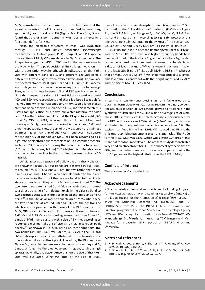
Magnified TEM images of synthesized MoS2 QDs are shown
in in Figure 1. The size distribution of MoS2 QDs ranges in 2‐9
Fig. 1 a) TEM image after PLAL process. b) Size distribution of MoS2 particles, which is dispersed in the range of 2‐9 nm with the average size of 4.2nm. c,d) HRTEM images of the MoS2 QDs.
Scheme 1 Schematic diagrams of the 3‐step PLAL process. a) MoS2powders are dispersed in a binary solvent of ethanol and water. b) Solution irradiated with laser pulses for 3‐5 min. MoS2 particles with sizes of 20‐50 nm are synthesized. c) MoS2 QDs with sizes of 2‐9 nm are obtained after irradiation for 20 min.
(a) (b) (c)
Journal Name ARTICLE
This journal is © The Royal Society of Chemistry 20xx J. Name., 2013, 00, 1‐3 | 3
Please do not adjust margins
Please do not adjust margins
nm (Figure 1b). The average size is 4.2 nm, which is close to the
reported Bohr radius for MoS2 (1–3 nm).27,28 According to the
definition of QD, i.e., particle radius≃Bohr radius of an exciton, the current QD can be confirmed as an actual QD. In addition,
the thickness of the MoS2 QDs was carefully measured with
AFM to be 3.6 nm, which corresponds to 3‐5 layers (Figure S2).
High‐resolution TEM (HRTEM) images of the MoS2 QDs are
displayed in Figure 1c‐d. Lattice fringes of 0.27 and 0.31 nm
spaces are observed, which correspond to the distance
between the (100) planes of MoS2 (0.27 nm).29 Thus, the PLAL
method employed in the current study successfully synthesized
crystalline MoS2 QDs. The result of XRD also indicates crystalline
MoS2 QDs (Figure S3). Here, let us note the previous studies on
MoS2 nanomaterials synthesized by PLAL. MoS2 NPs with 20 nm
QDs11 and fullerene‐like MoS2 NPs 10 were obtained from PLAL
using methanol and water as solvents, respectively; however,
smaller sized TMDs have not been synthesized by ns‐PLAL. By
changing the solvent for PLAL in the present study, the particle
size was reduced from 20 nm to 4 nm. MoS2 QDs with an
average size of 4 nm by PLAL in a binary solvent composed of
water and ethanol were thus obtained. The ultra‐small QDs
were generated in a binary solvent due to the following: i) a
principle reason is the use of a binary solvent, which acts as a
good solvent for MoS2. This is because excellent solubility is
established in the 45 vol% ethanol/water mixture,30 which is
responsible for the Hansen solubility parameters. ii) A
shockwave generated by the initial process of PLAL effectively
exfoliates MoS2 powders with the original size (2 μm) in the
good solvent. Water and/or ethanol molecules interact with the
edge of the delamination of MoS2, which triggers exfoliation
and fragmentation (ca. 50 nm). iii) Subsequent laser shots in the
binary solvent continue the process described in ii) which
results in sizes smaller than 5 nm, as shown in Figure 1 and S2.
(b) (c) (a) 0.5
0.4
0.3
0.2
0.1
0.0
Pot
entia
l (V
vs.
SH
E)
1.41.21.00.80.60.40.2
log (j) (mA cm2)
Au: 116±1
Bulk MoS2: 69±1.4
Pt: 34±0.4
MoS2 QDs: 49±1.6
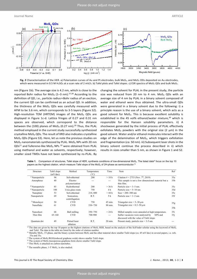
Table 1. Comparison of structures, Tafel slope of HER, synthesis conditions of low-dimensional MoS2. The listed dataa) focus on the top 10papers as the highest citation, which measure Tafel slope of the MoS2 of 2H-phase as semiconductor.b)
Structure Tafel slope
(mV/dec) Method Temperature
(°C) Time Note Ref
c) Nanoparticle 94 Solvothermal 200 > 10 h Citation # = 2753 (Nov. 7th, 2019) 35aAmorphous 40 Electro-
polymerization --- --- This sample is not a low dimensional material but a
thin film. 35b
d) Nanoparticle 85 Hydrothermal 200 > 36 h Particle size = 35 nm. 35ce) Nanoparticle 100 Urea-glass route 750 4 h Particle size = 510 nm 35d
Nanoplate 53 Solvothermal 210, 800 > 44 h Size = 200300 nm 35eNanoparticle 69 Sonication,
centrifugation R.T. 5 h Particle size = 12 nm 35f
f) Monolayer 50 CVD 750 45 min. Triangular size = 530 m Triangular size = 0.250 m
35g
35hNanoflake 61 CVD 530750 90 min.
Nanosheet Thin film
68 65-160
Ball milling CVD
350750 700-900
> 24 h ---
Milled samples were annealed at high temperature. Sulfur vacancies were analyzed by XPS and
35i35j
discussed with the value of Tafel slope. Quantum dot 49 Pulsed laser R.T. 20 min. Present study, particle size = 3-5 nm ---
ablation a) The data are given by the top 10 papers as the highest citations of MoS2 HER, based on the analysis of the SciFinder scholar using the keyword of MoS2
and Tafel. The data in the table are listed by the order of citation number. b) Metallic MoS2, 1T-phase, and the binary system between MoS2 and the other material show smaller Tafel slope (ca. 45 mV/dec) in several papers, i.e. refs.
35a and 35c. c) The system of MoS2/RGO(reduced graphene oxide) shows smaller Tafel slope. d) The system of MoS2/mesoporous-graphene-form shows smaller Tafel slope. e) This MoS2 is attached on carbon nanotubes. f) The metallic phase, 1-T MoS2, is also studied.

ARTICLE Journal Name
4 | J. Name., 2012, 00, 1‐3 This journal is © The Royal Society of Chemistry 20xx
Please do not adjust margins
Please do not adjust margins
In fact, larger‐sized particles are produced by PLAL with either
pure water or other neat organic solvents in the present study.
To evaluate the catalytic properties of ultra‐small MoS2 QDs,
electrochemical measurements for the HER were conducted,
and the results for MoS2 were compared with those for bulk
MoS2 and noble metals. Current density vs. the electric
potential applied to these materials is shown in Figure 2a. The
HER starts at the position where the voltage drops, and the HER
over MoS2 QDs occurs at a lower voltage than those of Au and
bulk MoS2. This indicates that MoS2 QDs act as better
electrocatalysts. To quantify the catalytic properties, Tafel plots
were analysed, as shown in Figure 2b. The MoS2 QDs have a very
small Tafel slope of 49±1.6 mV/dec. A smaller Tafel slope
indicates better catalysis of the HER; therefore, the MoS2 QDs
prepared in the present study act as a very good catalyst. Very
good electrocatalytic performance of MoS2 has been reported
for low‐dimensional MoS2, i.e., Tafel slopes of 50 mV/dec for
defect‐rich nanosheets,12a 87 mV/dec for defect‐free
nanosheets,12a and 69 mV/dec31 and 98 mV/dec32 for QDs. Note
that the Tafel slope for the MoS2 QDs in the present study
(49±1.6 mV/dec) is almost same as that for defect‐rich
nanosheets (50mV/dec).12 The excellent electrocatalysis of
defect‐rich MoS2 nanosheets is attributed to sulphur (S)
vacancies at active sites. 12,33,34a,c Furthermore, we compared
the current study with the top 10 papers of the highest citation
(table 1) of MoS2 HER.35 Therefore, the current study shows very
good Tafel slope and the shortest synthesis time of MoS2
nanomaterials.
To evaluate the defects in the present system, we
conducted ESR spectroscopy measurements, indicating a direct
observation of defect as a spin active species. The results are
shown in Figure 2c. The ESR spectrum of MoS2 QDs is in very
good agreement with that of MoS2 with S vacancies,12,34 and
also has the same g‐value of 2.00.34 The MoS2 QDs in the current
study have S vacancies, which also give excellent catalytic
properties and are consistent with the study on defect‐rich
(c)
(a) (b)
(d)
(e) (f)
(c) (d)
A1B1
C D
Journal Name ARTICLE
This journal is © The Royal Society of Chemistry 20xx J. Name., 2013, 00, 1‐3 | 5
Please do not adjust margins
Please do not adjust margins
MoS2 nanosheets.12 Furthermore, this is the first time that the
atomic concentration of S vacancy is quantified by measuring
spin density and its value is 1% (Figure S4). Therefore, it was
found that 1% of a point defect in MoS2 act as an excellent
functional defect for HER.
Next, the electronic structure of MoS2 was evaluated
through PL, PLE, and UV‐vis absorption spectroscopy
measurements. A photograph, PL‐PLE map, PL, and PLE spectra
of a solution of MoS2 QDs are shown, in Fig. 3 respectively. The
PL spectra range from 400 to 500 nm for the luminescence in
the blue region. The peak position shifts to longer wavelengths
with the excitation wavelength, which indicates that, the MoS2
QDs with different band gap Eg and different size QDs exhibit
different PL wavelengths when excited (vide infra). To evaluate
the spectral shapes, PL (Figure 3c) and PLE (Figure 3d) spectra
are displayed as functions of the wavelength and photon energy.
Thus, a mirror image between PL and PLE spectra is evident.
Note that the peak positions of PL and PLE are located at around
400 and 350 nm, respectively, and there is a large Stokes shift,
i.e., =50 nm, which corresponds to 0.44 eV. Such a large Stokes
shift has been observed in graphene QDs, and this large shift is
useful for application as a down converter material for solar
cells.36 Another distinct result is that the PL quantum yield (QY)
of MoS2 QDs is 3.8%, whereas those of bulk MoS2 and
monolayer MoS2 have been reported to be almost 0%1 and
0.4%1, respectively. Thus, the QY of the MoS2 QDs here is almost
10 times higher than that of the MoS2 monolayer. The reason
for the high QY of monolayer MoS2 has been recognized as a
high rate of electron‐hole recombination in a confined system,
such as a 2D monolayer.37 Taking the current size into account
(4.2 nm ≃ Bohr radius, 1‐3 nm),27, 28 a higher recombination rate
is expected to occur in a further confined system, such as a 0D
material.
UV‐vis absorption spectra of bulk MoS2 and the MoS2 QDs
are shown in Figure 3e. Four bands are observed in bulk MoS2
at around 678, 618, 454, and 410 nm, the two former bands are
named as A1 and B1 bands, which are attributed to the direct
transitions from the top of the valence hand to two excitonic
states, spin‐orbit splitting, at the Brillouin zone K point.38,39 The
two latter bands are named C and D bands, which are attributed
to a direct transition from deeper levels in the valance band to
two excitonic states, spin‐orbit splitting at the Brillouin zone M
point.38 In the UV‐vis absorption spectrum of MoS2 QDs, there
are two shoulders at around 340 and 370 nm, the positions of
which are in agreement with those of the PLE spectrum for
MoS2 QDs shown in Figure 3d. Furthermore, these positions at
3.65 eV and 3.35 eV are in good agreement with the B1 and A1
bands of MoS2 nanoclusters with a size of 3‐4 nm, according to
reported experimental data of size vs. UV‐vis absorption peak
energy,38a as shown in Fig. S6b. Based on these situations, the
two bands (340 nm, 3.65 eV; 370 nm, 3.35 eV) in the PLE and
UV‐vis absorption spectra are attributed to the transitions of
two excitonic states at the K point. Therefore, the PL spectra in
Figures 3c, result in luminescence via the transition of A1 and B1
bands, shifting into the blue wavelength region, to give a high
QY (3.8%). Finally, the dependence of Eg on the size of the MoS2
QDs was evaluated using the data of the size of MoS2
nanoclusters vs. UV‐vis absorption band (vide supra).38a Size
distribution, the full width at half maximum (FWHM) in Figure
1b, was 3.7‐4.9 nm, which gave Eg = 3‐4 eV, i.e. Eg=2.8‐3.2 eV
(A1) and 3.4‐3.7 eV (B1), according to Fig. S6b. Note that this
energy range is almost equal to the FWHM of the PLE spectra,
i.e., 3.4 eV (370 nm)3.9 eV (320 nm), as shown in Figure 3d.
As a final topic, let us note the Raman spectrum of bulk MoS2
and the MoS2 QDs. The lower and higher frequency bands have
been attributed to the in‐plane E12g and out‐of‐plane A1g modes,
respectively, and the increment between the bands is an
indicator of layer thickness.41,42 A narrower increment is shown
in the MoS2 QDs (Figure 3f), i.e., bulk MoS2 is 26.8 cm1, whereas
that of MoS2 QDs is 24.5 cm1, which corresponds to 3‐5 layers.
This layer size is consistent with the height measured by AFM
and the size of MoS2 QDs by TEM.
Conclusions
In summary, we demonstrated a fast and facile method to
obtain uniform‐sized MoS2 QDs using PLAL in the binary solvent.
The aqueous solution of 45% ethanol played a critical role in the
synthesis of ultra‐small MoS2 QDs with an average size of 4 nm.
These QDs showed excellent electrocatalytic performance for
the HER with a very small Tafel slope (49mV dec‐1), which was
attributed to many sulphur vacancies as much as 1%. The
excitons confined in the 4 nm MoS2 QDs caused blue PL and the
efficient recombination among electrons and holes. The PL QY
for the MoS2 QDs was 3.8%, which was almost 10 times higher
than that for MoS2 monolayer. The present study demonstrated
very good electrocatalyst for HER, the shortest synthesis time of
QDs, and room‐temperature process in comparison with the
top 10 papers as the highest citations as the HER of MoS2.
Conflicts of interest
There are no conflicts to declare.
Acknowledgements
K.S. acknowledges financial support from the Funding Program
for the Next Generation World‐Leading Researchers (GR073) of
the Japan Society for the Promotion of Science (JSPS), a Grant‐
in‐Aid for Scientific Research (A) (15H02001) and (B)
(19H02556) from JSPS, the PRESTO Structure Control and
Function program of the Japan Science and Technology Agency
(JST), and JKA through its promotion funds from AUTORACE. We
acknowledge Dr. Maeda for measuring TEM images and Mrs.
Kawata for measuring ESR spectra at N‐BARD Hiroshima
University.
Notes and references
1 K. F. Mak, C. Lee, J. Hone, J. Shan and T. F. Heinz, Phys. Rev. Lett., 2010, 105, 136805.
2 A. Splendiani, L. Sun, Y. Zhang, T. Li, J. Kim, C. Y. Chim, G. Galli and F. Wang, Nano Lett., 2010, 10, 1271.
ARTICLE Journal Name
6 | J. Name., 2012, 00, 1‐3 This journal is © The Royal Society of Chemistry 20xx
Please do not adjust margins
Please do not adjust margins
3 a) J. N. Coleman, and V. Nicolosi et al, Science., 2011, 331, 568. b) M. Sakamoto, K. Saitow, Nanoscale, 2018, 10, 22215.
4 W.K. Hsu, B.H. Chang, Y.Q. Zhu, W.Q. Han, H. Terrones, M. Terrones, N. Grobert, A.K. Cheetham, H.W. Kroto, D.R. Walton, J. Am. Chem. Soc., 2000, 122, 10155.
5 S. Balendhran, J. Z. Ou, M. Bhaskaran, S. Sriram, S. Ippolito, Z. Vasic, E. Kats, S. Bhargava, S. Zhuiykov and K. Kalantar‐zadeh, Nanoscale, 2012, 4, 461.
6 Z. Liu, Y. B. Wang, Z. Y. Wang, Y. G. Yao, J. Q. Dai, S. Das and L. B. Hu, Chem. Commun., 2016, 52, 5757.
7 Y. Zhan, Z. Liu, S. Najmaei, P.M. Ajayan, J. Lou, Small., 2012, 8, 966.
8 Y. C. Lin, W. J. Zhang, J. K. Huang, K. K. Liu, Y. H. Lee, C. T. Liang, C. W. Chu and L. J. Li, Nanoscale, 2012, 4, 6637.
9 J. Jeon, S. Jang, S. Jeon, G. Yoo, Y. Jang, J.‐H. Park and S. Lee, Nanoscale, 2015, 7, 1688.
10 H.H. Wu, R. Yang, B.M. Song, Q.S. Han, J.Y. Li, Y. Zhang, Y. Fang, R. Tenne and C. Wang, ACS Nano., 2011, 5, 1276.
11 T. Oztas, H. S. Sen, E. Durgun, B. Ortac, J. Phys. Chem. C., 2014, 118, 30120.
12 a) J. Xie, H. Zhang, S. Li, R. Wang, X. Sun, M. Zhou, J. Zhou, X.W. Lou, Y. Xie, Adv Mater., 2013, 25 5807. b) G. Ye, Y. Gong, J. Lin, B. Li, Y. He, S. T. Pantelides, W. Zhou, R. Vajtai, P. M. Ajayan, Nano Lett. 2016, 16, 1097.
13 X. Lu, M. I. Utama, J. Zhang, Y. Zhao and Q. Xiong, Nanoscale, 2013, 5, 8904.
14 Y. W. Lihui, H. Yu, X. R. Yang, J. J. Zhou, Q. Zhang, Y. Q. Zhang, Z. M. Luo, S. Su and L. H. Wang, Chem. Commun., 2016, 52, 529.
15 D.Z. Wang, Z. Pan, Z. Z. Wu, Z.P. Wang, Z.H. Liu, J. Power Sources., 2014, 264,229.
16 a) Deepesh, G., Dijo, D. & Shaijumon, M. M. Acs Nano.8, 5297 (2014), b) Xu, S., Li, D. & Wu, P, Adv. Funct. Mater. 2015, 25, 1127. c) D. Gopalakrishnan, D. Damien, B. Li, H. Gullappalli, V. K. Pillai, P. M. Ajayanb and M. M. Shaijumon, Chem. Commun., 2015, 51, 6293.
17 Publications were surveyed by SciFinder scholar. Specifically, the number of publications of studies on “MoS2 quantum dot” and “MoS2 monolayer” were 33 and 544, both of which were analysed by selecting document type (paper, letter, and review) and language (English).
18 a) D. Zhang, B. Gökce, S. Barcikowski, Chem. Rev., 2017, 117, 3990. b)B. Gökce, V. Amendola, S. Barcikowski, ChemPhysChem, 2017, 18, 983. c) D. Zhang, J. Liu, P. Li, Z. Tian, C. Liang, ChemNanoMat, 2017, 3, 512. d) M. R. Kalus, R. Lanyumba, N. Lorenzo‐Parodi, M. A. Jochmann, K. Kerpen, U. Hagemann, T. C. Schmidt, S. Barcikowski, B. Gökce, Phys. Chem. Chem. Phys., 2019, 21, 18636.
19 a) D. Kajiya, K. Saitow., RSC Adv., 2018, 8, 41299. b) Y. Xin, T. Kitasako, M. Maeda, and K. Saitow, Chem. Phys. Lett., 2017, 674, 90. c) Y. Xin, K. Nishio and K. Saitow, Appl. Phys. Lett., 2015, 106, 201102,d) T. Kitasako and K. Saitow, Appl. Phys. Lett., 2013, 103, 151912.
20 a) K. Saitow, Y. Okamoto, H. Suemori, ACS Omega, 2019, 4, 14307. b) S. Wei, T. Yamamura, D. Kajiya, K. Saitow, J. Phys. Chem. C 2012, 116, 3928; c) K. Saitow, Y. Okamoto, Y. F. Yano, J. Phys. Chem. C., 2012 116, 17252, d) K. Saitow, T. Yamamura, J. Phys. Chem. C., 2009, 113, 8465, e) K. Saitow, T. Yamamura, T. Minami, J. Phys. Chem. C, 2008, 112, 18340; f) K. Saitow, J. Phys. Chem. B., 2005, 109, 3731.
21 a) J. Lv, S. Wu, Z. Tian, Y. Ye, J. Liu& C. Liang, J. Mater. Chem. A, 2019, 7, 12627‐12634. b) C. L. Sajti, R. Sattari, B. N. Chichkov, S. Barcikowski, Appl. Phys. A, 2010, 100, 203, c) Y. Ishikawa, N. Koshizaki, Sci. Rep., 2018, 8, 14208.
22 S. Alkis, T. Öztas, L. E Aygün, F. Bozkurt, A. K. Okyay, & B Ortaç, J. Optics express, 2012, 20, 21815.
23 H. G. Baldoví, M. Latorre‐Sánchez, I. Esteve‐Adell, A. Khan, A. M. Asiri, S. A. Kosa, H. Garcia, J. Nanoparticle Res. 2016, 18, 240.
24 G. Ou, P. Fan, X. Ke, Y. Xu, K. Huang, H. Wei, W. Yu, H. Zhang, M. Zhong, H. Wu, Y. Li, Nano Res., 2018, 11, 751.
25 V. Nguyen, Q. Dong, L. Yan, N. Zhao, P. H. Le, J. Lumines. 2019, 214, 116554.
26 Z.Z. Wu, B.Z. Fang, D.Z. Wang, D.P. Wikinson et al, ACS Catal. 2013, 3, 2101.
27 R. Doolen, R. Laitinen, F. Parsapour, and D. F. Kelley, J. Phys. Chem. B., 1998, 102, 3906.
28 (a) R. Li, X. Dong, Z. Li, Z. Wang, Solid State Commun., 2018, 275, 53. (b) M.L. Trolle, T.G. Pedersen, V. Véniard, Sci. Rep. 2017, 7, 39844.
29 Y. H. Lee, X. Q. Zhang, W. Zhang, M. T. Chang, C. T. Lin, K. D. Chang, Y. C. Yu, J. T.‐W. Wang, C. S. Chang, L. J. Li and T. W. Lin, Adv. Mater., 2012, 24, 2320.
30 K. G. Zhou, N. N. Mao, H. X. Wang, Y. Peng, & H. L. Zhang, Angew. Chem. Int. Ed, 2011, 50, 10839.
31 S. Das, R. Ghosh, P. Routh, A. Shit, S. Mondal, A. Panja and A. K. Nandi, ACS Appl. Nano Mater., 2018, 1, 2306
32 L. Najafi, S. Bellani, B. Martín‐García, R. Oropesa‐Nuñez, A. E. Del Rio Castillo, M. Prato, I. Moreels and F. Bonaccorso, Chem. Mater., 2017, 29, 5782.
33 G. Li, D. Zhang, Q. Qiao, Y. Yu, D. Peterson, A. Zafar, R. Kumar, S. Curtarolo, F. Hunte, S. Shannon, Y. Zhu, W. Yang and L. Cao, J. Am. Chem. Soc., 2016, 138, 16632.
34 a) B. Deroide, Y. Bensimon, P. Belougne, J. V. Zanchetta, J. Phys. Chem. Solids, 1991, 52, 853. b) Y. Yin, J. Han, Y. Zhang, X. Zhang, P. Xu, Q. Yuan, L. Samad, X. Wang, Y. Wang, Z. Zhang, P. Zhang, X. Cao, B. Song, and S. Jin, J. Am. Chem. Soc. 2016, 138, 7965. c) L. Cai, J.F. He, Q.H Liu, T. Yao, L. Chen, W. S. Yan, F.C. Hu, Y. Jiang, Y.D. Zhao, T.D. Hu, Z.H. Sun, S.Q. Wei, J. Am. Chem. Soc., 2015 137, 2622.
35 a) Y. Li, H. Wang, L. Xie, Y. Liang, G. Hong, H. Dai, J. Am. Chem. Soc. 2011, 133, 7296. b) D. Merki, S. Fierro, H. Vrubel, X. Hu, Chem. Sci., 2011, 2, 1262. c) L. Liao, J. Zhu, X. Bian, L. Zhu, M. D. Scanlon, H. H. Girault, B. Liu, Adv. Funct. Mater. 2013, 23, 5326. d) D. H. Youn, S. Han, J. Y. Kim, J. Y. Kim, H. Park, S. H. Choi, J. S. Lee, ACS nano, 2014, 8, 5164. e) Y. Yan, B.Y. Xia, X. Ge, Z. Liu, J. Wang, X. Wang, ACS Appl. Mater. Interfaces 2013, 5, 12794. f) T. Wang, L. Liu, Z. Zhu, P. Papakonstantinou, J. Hu, H. Liu, M. Li, Energy Environ. Sci., 2013, 6, 625. g) D. Voiry, R. Fullon, J. Yang, C. d. C. C. e Silva, R. Kappera, I. Bozkurt, D. Kaplan, M. J. Lagos, P. E. Batson, G. Gupta, A. D. Mohite, L. Dong, D. Er, V. B. Shenoy, T. Asefa, M. Chhowalla, Nat. Mater., 2016, 15, 1003. h) J. Shi, D. Ma, G. Han, Y. Zhang, Q. Ji, T. Gao, J. Sun, X. Song, C. Li, Y. Zhang, X. Lang, Y. Zhang, Z. Liu, ACS nano, 2014, 8, 10196. j) Z. Wu, B. Fang, Z. Wang, C. Wang, Z. Liu, F. Liu, W. Wang, A. Alfantazi, D. Wang, D. P. Wilkinson, ACS Catal. 2013, 3, 2101. i) G. Li, D. Zhang, Q. Qiao, Y. Yu, D. Peterson, A. Zafar, R. Kumar, S. Curtarolo, F. Hunte, S. Shannon, Y. Zhu, W. Yang, L. Cao, J. Am. Chem. Soc. 2016, 138, 16632.
36 F. Khan, J.H. Kim. ACS Photo., 2018, 5, 4637. 37 M. Amani, D. Lien, D. Kiriya, J. Xiao, A. Azcatl, J. Noh, S.R.
Madhvapathy, R. Addou, S. Kc, M. Dubey, K. Cho, R.M. Wallace, S. Lee, J. He, J.W.A. Iii, X. Zhang, E. Yablonovitch, A. Javey. Science 2015, 350, 1065.
38 a) J.P. Wilcoxon, P.P. Newcomer, G. A. Samara. J. Appl. Phys., 1997, 81, 7934. b) R. F. Frindt, A. D. Yoffe, Proc. R. Soc. London, Ser. A 1963, 273, 69. c) A. Splendiani, L. Sun, Y. Zhang, T. Li, J. Kim, C. Chim, G. Galli, F. Wang, Nano Lett. 2010, 10, 1271. d) R. F. Frindt, Phys. Rev. 1965, 140, A536. e) G. Eda, H. Yamaguchi, D. Voiry, T. Fujita, M. Chen, M. Chhowalla, Nano Lett. 2011, 11, 5111. f) R. Ahmad, R. Srivastava, S. Yadav, D. Singh, G. Gupta, S. Chand, S. Sapra, J. Phys. Chem. Lett. 2017, 8, 1729.
39 The optical transitions of A1 and B1 are considered as direct transitions for monolayer, whereas those of a bulk MoS2 are attributed as indirect transitions, described in refs. 38c and 40.
Journal Name ARTICLE
This journal is © The Royal Society of Chemistry 20xx J. Name., 2013, 00, 1‐3 | 7
Please do not adjust margins
Please do not adjust margins
40 a) K. F. Mak, C. Lee, J. Hone, J. Shan, T. F. Heinz, Phys. Rev. Lett., 2010, 105, 136805. b) A. Molina‐S´anchez, D. Sangalli, K. Hummer, A. Marini, L. Wirtz, Phys, Rev. B 2013, 88, 045412.
41 Radisavljevic, A. Radenovic, C. Lee, H. Yan, L. Brus, T. F. Heinz, J. Mone, S. Ryu, ACS Nano, 2010, 4, 2695.
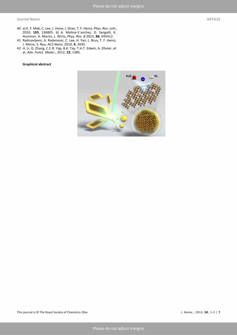
42 H. Li, Q. Zhang, C.C.R. Yap, B.K. Tay, T.H.T. Edwin, A. Olivier, et al. Adv. Funct. Mater., 2012, 22, 1385. Graphical abstract