19980130 146 - Defense Technical Information Center · Master of Science in Electrical Engineering...
101
AFIT/GE/ENG/97D- 16 Pseudorandom Code Generation for Communication and Navigation System Applications THESIS John F. Brendle Jr. Captain, USAF MC QUALITY INN2CTV AFIT/GE/ENG/97D-16 19980130 146 Approved for public release; distribution unlimited
Transcript of 19980130 146 - Defense Technical Information Center · Master of Science in Electrical Engineering...
AFIT/GE/ENG/97D- 16
Pseudorandom Code Generation forCommunication and Navigation System Applications
THESIS
John F. Brendle Jr.Captain, USAF MC QUALITY INN2CTV
AFIT/GE/ENG/97D-16
19980130 146
Approved for public release; distribution unlimited

The views expressed in this thesis are those of the author and do not reflect the official policy or positionof the Department of Defense of the United States Government.
AFIT/GE/ENG/97D- 16
Pseudorandom Code Generation forCommunication and Navigation System Applications
THESIS
Presented to the Faculty of the School of Engineering
of the Air Force Institute of Technology
Air University
In Partial Fulfillment of the
Requirements for the Degree of
Master of Science in Electrical Engineering
John F. Brendle Jr., B.S.E.E.
Captain, USAF
December, 1997
Approved for public release; distribution unlimited

AFIT/GEIENG/97D-16
Pseudorandom Code Generation forCommunication and Navigation System Applications
John F. Brendle Jr., B.S.E.E.
Captain, USAF
Approved: P 1
MaiMclhael A. Temple, Ph. II. DateChairman
Lt. Col. (s) Donald S. Gelosh, Ph. D. DateCommittee ber
Dr. Martin P. DeSimio DateCommittee Member

Acknowledgements
After spending countless hours on this project over the past year, I would like to
thank those who have supported me. I would like to first thank my thesis advisor, Major
Michael A. Temple, for all of his guidance in the interface design. I would also like to
thank my committee members, Lt Col (s) Donald S. Gelosh and Dr. Martin P. DeSimio,
for their support. I would like to thank my sponsor, James P. Stephens Sr., for his
assistance in developing the idea for this project. I can not forget to thank my classmates
who also lived in the Communications and Radar Lab. Finally, I would like to thank my
wife, Heather, and children, Johnathan, Katharine, and Elisabeth, for their support and
understanding.
John F. Brendle Jr.
Wli

Table of Contents
PageAcknowledgements ...................................................................................................... i
List of Figures ............................................................................................................... vii
List of Tables ................................................................................................................. ix
Abstract .......................................................................................................................... x
1. Introduction ............................................................................................................. 1-11.1 Background ......................................................................................................... 1-11.2 Problem Statement .............................................................................................. 1-31.3 Scope .................................................................................................................. 1-31.4 M aterials and Equipment ..................................................................................... 1-31.5 Thesis Organization ............................................................................................. 1-3
2. Pseudorandom Sequences ........................................................................................ 2-12.1 Pseudonoise/Pseudorandom sequences ................................................................ 2-1
2.1.1 Balance Property ........................................................................................... 2-12.1.2 Run Property ................................................................................................. 2-22.1.3 Correlation Property ...................................................................................... 2-2
2.2 Shift Registers ..................................................................................................... 2-32.2.1 Feedback Taps .............................................................................................. 2-4
2.2.1.1 M aximal Length Sequences ..................................................................... 2-62.2.1.1.1 Properties of Maximal Length Sequences ................... 2-7
2.3 Composite Codes ................................................................................................ 2-82.3.1 Gold Code Sequence Generator .................................................................... 2-9
2.3.1.1 GPS Gold Code Generation .................................................................. 2-102.3.2 JPL Ranging Code Generator ...................................................................... 2-122.3.3 Syncopated-Register Generator ................................................................... 2-13
2.4 N on-Linear Codes ............................................................................................. 2-15
3. System D esign .......................................................................................................... 3-13.1 System Overview ................................................................................................ 3-1
3.1.1 STEL-1032 Inputs ........................................................................................ 3-43.1.1.1 ADDRo - ADDR7 .............................................. . . . . . . . . . . . . . . . . . . . . . . . . . . . . . . . . . . .. . . 3-5
3.1.1.1.1 M ask Register ................................................................................... 3-63.1.1.1.2 INIT Register .................................................................................... 3-63.1.1.1.3 EPOCH Register ............................................................................... 3-63.1.1.1.4 COUNT Register .............................................................................. 3-73.1.1.1.5 Phase M UX Register ......................................................................... 3-7
iv
3.1.1.1.6 CTL Register .................................................................................... 3-73.1.1.1.7 Code Combiner Lookup Register ...................................................... 3-8
3.1.1.2 D ATA0 - D ATA7 .................................................................................... 3-93.1.1.3 Reset ....................................................................................................... 3-93.1.1.4 CLK0 - CLK2 ................................................. . . . . . . . . . . . . . . .. . . . . . . . . . . . . . . . . . . . . . . . . . 3-93.1.1.5 W RN and CSN ..................................................................................... 3-103.1.1.6 LOADo - LOAD 2 ............................................. . . . . . . . . . . . . . . . . . . . . . . . . . .. . . . . . . . . . . 3-103.1.1.7 STIM o - STIM 2 and STLD .................................................................... 3-10
3.1.2 STEL-1032 Outputs .................................................................................... 3-103.1.2.1 CODE0 - CODE2 ............................................. . . . . . . . . . . . . . . . . . . . . . . . . . .. . . . . . . . . . . 3-113.1.2.2 M OD CODo - M OD COD 2 ...................................... . . . . . . . . . . . . . . . . . . . . . . . . . . . . . . . 3-113.1.2.3 LD SYN CO - LD SYN C2 ........................................ . . . . . . . . . . . . . . . . . . . .. . . . . . . . . . . . . 3-113.1.2.4 REF150 - REF15 2 ............................................. . . . . . . . . . . . . . . . . . . . . . . . . . . . . . . . . . . . . . 3-113.1.2.5 EPOCHo - EPOCH2 ........................................... . . . . . . . . . . . . . . . . . . . . . . . . . . . . . . . . . . . 3-113.1.2.6 COUNT0 - COUNT 2 .......................................... . . . . . . . . . . . . . . . . . . . . . . . . . . . . . . . . . . . 3-123.1.2.7 XORoi and XOR0 12 ........................................... . . . . . . . . . . . . . . . . . . . . . . . . . . . . . . . . . . . . 3-123.1.2.8 M IX COD .............................................................................................. 3-123.1.2.9 PUN CT, EARLY, and LATE ................................................................ 3-123.1.2.10 STSYN C ............................................................................................ 3-13
3.2 Code Generator Addressing D esign ................................................................... 3-133.2.1 Coder Selector D esign ................................................................................ 3-153.2.2 Register Selector D esign ............................................................................. 3-163.2.3 32 or 8 bit D ata Address .............................................................................. 3-17
3.3 Code Generator D ata Entry D esign ................................................................... 3-193.3.1 D ata Buffer Enable D esign .......................................................................... 3-203.3.2 D ata Entry Form at ...................................................................................... 3-21
3.4 Code Generator D ata Loading ........................................................................... 3-223.5 Other Code Generator Inputs ............................................................................ 3-243.6 Code Generator Outputs ................................................................................... 3-243.7 Code Generator Construction ............................................................................ 3-253.8 Code Generator System D esign Summ ary ......................................................... 3-27
4. Code Generator Evaluation ...................................................................................... 4-14.1 Code Generator Loading Pulses ........................................................................... 4-14.2 Coder Outputs ..................................................................................................... 4-3
4.2.1 Pseudorandom Output Code D em onstration .................................................. 4-44.2.2 LD SYN C Pulse Output D em onstration ......................................................... 4-64.2.3 COUNT Pulse Output D em onstration ........................................................... 4-64.2.4 EPOCH Pulse Output D em onstration ............................................................ 4-74.2.5 Pseudorandom Code at REF 15 D em onstration .............................................. 4-84.2.6 M OD COD Output W aveform D em onstration ................................................ 4-9
4.3 Code Combiner Outputs ...................................................................................... 4-94.3.1 X ORO1 Output W aveform D em onstration ................................................... 4-11
V

4.3.2 XORO12 Output W aveform D emonstration ................................................. 4-134.3.3 MI XCOD Output W aveform Dem onstration ............................................... 4-144.3.4 PUNCT, EARLY, and LATE Output Waveform Demonstration ................. 4-15
4.4 Special Codes .................................................................................................... 4-174.5 Code Generator Evaluation Summ ary ................................................................ 4-20
5. Conclusions and Recommendations ..................................................................... 5-15.1 Conclusions ......................................................................................................... 5-15.2 Recomm endations for Future Study ..................................................................... 5-2
Appendix A : Octal Representation of Primitive Generator Polynomials ................. A-1
Appendix B : Parts Listing and Circuit D iagram ................................................... B-i
Bibliography .......................................................................................................... BIB-i
Vita ...................................................................................................................... VITA-1
Vi
List of Figures
Figure 2-1. Linear Feedback Shift Register .................................................................. 2-4Figure 2-2. Gold Code Sequence Generator Configuration ........................................ 2-10Figure 2-3. C/A Code G eneration .............................................................................. 2-11Figure 2-4. Typical JPL Code Sequence Generator Configuration .............................. 2-13Figure 2-5. Syncopated Code Generator .................................................................... 2-14Figure 2-6. Syncopated Code Example ...................................................................... 2-14
Figure 3-1. STEL-1032 Block Diagram ....................................................................... 3-2Figure 3-2. Individual Coder Block Diagram ................................................................ 3-3Figure 3-3. Registers Connections of Individual Coder ................................................ 3-4Figure 3-4. Address Block Diagram ........................................................................... 3-14Figure 3-5. Coder Selector D esign ............................................................................. 3-15Figure 3-6. Register Selector D esign .......................................................................... 3-16Figure 3-7. Clock and Counter Design ....................................................................... 3-18Figure 3-8. ADDR1 and ADDR0 Generation ............................................................. 3-18Figure 3-9. Data Entry Design Block Diagram ........................................................... 3-19Figure 3-10. Data Buffer Enabling Design ................................................................. 3-21Figure 3-11. Load Pulse D esign ................................................................................. 3-22Figure 3-12. Data Loading Pulse Comparison ............................................................ 3-23Figure 3-13. O utput D esign ....................................................................................... 3-25Figure 3-14. Code Generator Case Layout ................................................................. 3-25Figure 3-15. Code Generator Front Panel .................................................................. 3-26Figure 3-16. Code Generator Circuit Board ............................................................... 3-26
Figure 4-1. Code Generator Data Loading Clock ......................................................... 4-1Figure 4-2. Data Loading Clock, CSN, and WRN Pulses ............................................. 4-2Figure 4-3. Test Linear Feedback Shift Register ........................................................... 4-3Figure 4-4. CODEO and Input Clock ........................................................................... 4-5Figure 4-5. Multiple Periods of CODEO and Clock Pulse ............................................. 4-5Figure 4-6. CODEO and LDSYNC Pulse ..................................................................... 4-6Figure 4-7. CODE0 and COUNT Pulse ....................................................................... 4-7Figure 4-8. CODEO and EPOCH Pulse ........................................................................ 4-7Figure 4-9. CODEO at Tap Number 2 and REF 15 ........................................................ 4-8Figure 4-10. CODEO and MODCOD ........................................................................... 4-9Figure 4-11. Test Linear Feedback Shift Register (Coderl and Coder2) ..................... 4-10Figure 4-12. CODEO, CODE1, and XORO1 .............................................................. 4-11Figure 4-13. Gold Code and Nonmaximal Pseudorandom Code ................................. 4-12Figure 4-14. CODE0, CODE1, and Gold Code .......................................................... 4-13Figure 4-15. Code0, Codel, Code2, and XOR012 ..................................................... 4-14Figure 4-16. MODCOD0 - MODCOD 2 and MIXCOD ............................................... 4-15Figure 4-17. MIXCOD and PUNCT Outputs ............................................................ 4-16
vii

Figure 4-18. PUNCT and EARLY Outputs ............................................................... 4-16Figure 4-19. PUNCT and LATE Outputs ................................................................. 4-17Figure 4-20. Truncated CODEO and EPOCH Pulse ................................................... 4-18Figure 4-21. Truncated CODEO and Coderl EPOCH Pulse ....................................... 4-18Figure 4-22. CODE1 and CODEO with CODE1 Clock Input ..................................... 4-19
Figure A-1. 3 Stage Linear Feedback Shift Register ................................................ A-1
viii
List of Tables
Table 2-1. Linear Feedback Shift Register Sequence .................................................... 2-5Table 2-2. Number of Maximal Sequences and Code Lengths Available from Register
L engths 2 through 32 ............................................................................................. 2-6
Table 3-1. Address bits ADDR7 - ADDR 5 ........................................ . . . . . . . . . . . . . . . . . . .. . . . . . . . . 3-5Table 3-2. Address bits ADDR4 - ADDRo .................................................................... 3-5Table 3-3. Address bit ADDR, - ADDRO for 32 bit DATA .......................................... 3-6Table 3-4. Control (CTL) Register Bit Functions: (a) B 7-B6, (b) B5-B4, (c) B 3 -B2, ....... 3-8Table 3-5. Code Combiner Lookup Register Table ...................................................... 3-9Table 3-6. 8-Line to 3-Line Priority Encoder Function Table ..................................... 3-15Table 3-7. Tri-State Octal Buffer Outputs .................................................................. 3-20
Table 4-1. Linear Feedback Shift Register State Values ............................................... 4-4Table 4-2. Linear Feedback Shift Register State Values ............................................. 4-10Table 4-3. Exam ple Look-up Table ............................................................................ 4-15
Table A-1. Octal Representation of Primitive Generator Polynomials .......................... A-2
Table B -1. Parts Listing ........................................................................................ B -i
ix
AFIT/GE/ENG/97D- 16
Abstract
This research project investigated the design, construction and evaluation of a
pseudorandom code generator for communication and navigation system applications.
These types of codes include spreading codes, Gold codes, Jet Propulsion Laboratory
(JPL) ranging codes, syncopated codes, and non-linear codes. Such waveforms are
typically used in communication and navigation systems applications. The code generator
uses the Stanford Telecom STEL-1032 Pseudorandom Number (PRN) coder. A coder
interface was designed and constructed for manual data entry to the registers of the PRN
coder. The code generator is capable of independently clocking and generating all
possible codes with lengths up to 232-1 (4,294,967,295). The codes can be started with
any random phase. The code generator is capable of detecting a specific position in the
code and the coders can be truncated and restarted at that point. The three independent
coder outputs are combinable, expanding the lengths and versatility of the codes. The
generation of a non-linear code is possible using an internally programmable look-up table.
Several tests were conducted on the code generator to ensure its capability of generating
the spreading codes, gold codes, JPL ranging codes, syncopated codes, and non-linear
codes. The required documentation is being submitted for a U.S. patent.
x

1. Introduction
1.1 Background
Spread Spectrum (SS) communications grew out of research efforts during World
War II to provide secure means of communications in hostile environments [4]. During
the early years of spread spectrum investigation, one technique considered for operating a
transmitter and receiver synchronously with a truly random spreading signal was the
Transmitted Reference (TR) system. In a TR system, the transmitter sends two versions
of an unpredictable wideband carrier, one modulated by data and the other unmodulated,
which are transmitted on separate channels. At the receiver, the unmodulated carrier is
used as a reference signal for despreading the data-modulated carrier. The principal
advantage of a TR system is there are no significant synchronization problems at the
receiver, since the spread data-modulated signal and the despreading waveform are
transmitted simultaneously. The principle disadvantage of TR systems is the spreading
code is sent in the clear and thus is available to any listener. As such, the system is easily
spoofed by a jammer capable of sending a pair of waveforms acceptable to the receiver.
Other disadvantages include 1) performance degradation at low signal levels due to noise
being present on both transmitted signals and 2) twice the bandwidth and transmitted
power are required because of the need to transmit the reference [6].
Modem spread spectrum systems use a technique called Stored Reference (SR)
whereby the spreading and despreading waveforms are independently generated at the
transmitter and receiver, respectively. The main advantage of an SR system is that a well-
1-1

designed code signal cannot be predicted by an unintended receiver monitoring the
transmission [6]. The noiselike code signals used in SR systems cannot be "truly random"
as in the case of a TR system. Rather, signals which possess noiselike properties called
pseudonoise (PN) or pseudorandom signals, are employed as the spreading waveforms.
While a random signal cannot be predicted, a pseudorandom signal is not random at all; it
is a deterministic, periodic signal that is known to both the transmitter and receiver. Even
though the signal is deterministic, it appears to have the statistical properties of sampled
white noise and appears to the unauthorized listener as a truly random signal.
A linear feedback shift register is often used to generate the pseudorandom spreading
code. The shift register operation is controlled by a sequence of clock pulses. At each
clock pulse, the contents of each stage in the register are shifted one stage to the right and
fed back through of series of interconnected taps. The shift register sequence is usually
defined as the output of the last stage. The shift register sequence is dependent on the
number of stages, the feedback tap connections, and the initial conditions (starting phase).
The output sequence is classified as either maximal length or nonmaximal length. A
maximal length sequence has the property that for an n-stage linear feedback shift register,
the sequence repetition period (in clock pulses p) is p = 2 - 1. If the sequence length is
less than (2 n - 1), the sequence is classified as a nonmaximal length sequence.
1-2
1.2 Problem Statement
The purpose of this study is to design a pseudorandom code generator for
communication and navigation system applications. This thesis addresses the need for a
flexible, highly efficient, means of providing pseudorandom signals for test, evaluation and
development of multiple systems. In addition, the ability to explore and validate new
pseudorandom codes is addressed.
1.3 Scope
The design, construction, and evaluation of the system has enormous possibilities.
Due to time constraints, it was necessary to put limitations on the project. The system
was designed for a computer interface but has yet to be implemented; a manual data entry
and addressing technique was developed for system testing. Several test code and
scenarios are analyzed and presented in Chapter 4.
1.4 Materials and Equipment
Appendix B contains the complete materials list and design schematics used in this
project. A great deal of the materials and equipment used for construction and
evaluations were provided by the Avionics Directorate of Wright Laboratories. Other
items were procured by out of pocket expenses.
1.5 Thesis Organization
Chapter 2 presents a background on spread spectrum signal codes and the PRN
coder capabilities. This chapter also includes a description of different types of spreading
1-3

codes that can be generated with this project and examples of their application. In
Chapter 3, the capabilities, performance, and operation of the STEL-1032 are fully
described and the interface design is presented and analyzed. Chapter 4 begins with an
explanation on operating the system and concludes with the analysis of several test
outputs. The conclusion and recommendations are included in Chapter 5. Appendix A
includes a table with feedback connections for generation of maximal length sequences.
Appendix B shows the complete circuit diagram for the system including a parts listing.
1-4

2. Pseudorandom Sequences
2.1 Pseudonoise/Pseudorandom sequences
In the Transmitted Reference (TR) system, a truly random code can be utilized for
spreading and despreading since the code signal and data-modulated code signal are
simultaneously transmitted over different regions of the spectrum. The Stored Reference
(SR) approach cannot use a truly random code signal because a copy of the code needs to
be stored or generated at the receiver. For a SR system, a pseudonoise or pseudorandom
code is typically used. A truly random signal is unpredictable and future variations can
only be described in a statistical sense. However, a pseudorandom signal is not really
random -- it is a deterministic periodic signal that is known to both the transmitter and
receiver. Even though the signal is deterministic, it possess statistical properties consistent
with sampled white noise and appears to be truly random to an unauthorized listener.
There are three basic properties that can be applied to any periodic binary sequence as a
test for the appearance of randomness. These properties are called balance, run and
correlation [6]. If all three properties are satisfied, the sequence is classified as a
pseudorandom sequence.
2.1.1 Balance Property
Good balance requires that within each period of the sequence, the number of
binary ones differ from the number of binary zeros by at most one digit. As an example,
2-1

the sequence ( 0 0 0 1 0 0 11 0 1 0 1 1 1 1) has seven zeros and eight ones, satisfying the
balance property.
2.1.2 Run Property
A run is defined as a sequence of a single type of binary digit(s). The appearance
of the alternate digit in a sequence starts a new run. The length of the run is defined as the
number of digits in the run. Among the runs of ones and zeros in each sequence, it is
desirable that about one-half the runs of each type are of length 1, about one-fourth are of
length 2, one-eighth are of length 3, and so on. Considering the runs of zeros in the
previous example, there are two (one-half) of length 1, one (one-quarter) of length 2, and
one of length 3. Considering the runs of ones, there are two (one-half) of length 1, one
(one-quarter) of length 2, and one of length 4. The sequence satisfies the run condition.
2.1.3 Correlation Property
If a single period of the sequence is compared term-by-term with any cyclic shift of
itself, it is desirable that the number of agreements differs from the number of
disagreements by not more than one count. Below is a bit-by-bit comparison of the
example sequence with a single end-around shift of itself.
000100110101111100010011010111daaddadadddd aaa
2-2

Digits that agree are labeled a and those that disagree are labeled d. As shown, the
number of agreements (7) differ from the number of disagreements (8) by 1. It is easily
shown that the example sequence satisfies the correlation property for any cyclic shift.
Given the example sequence of (0 0 0 1 0 0 11 0 1 0 1 1 1 1) satisfies the balance, run,
and correlation properties, it is classified as a pseudorandom sequence.
2.2 Shift Registers
Many system applications require pseudorandom sequences. A convenient and
simple method for generating sequences which appear random and posses the
characteristics described in Section 2.1 is required. It is also desirable that the same
apparatus, when operated in an identical manner, produces the same sequence and that the
generator be as simple as possible. Such a sequence is easily generated using a feedback
shift register configuration.
A shift register is the arrangement of n stages, called delay elements, in a row.
Each stage contains either an "on" (1) or "off' (0); the contents of each stage are shifted
to the next stage, in time with a clock pulse. If no new signals are introduced into the first
stage during the shifting process, by the end of n shifts all of the stages will be "off' and
will remain that way. One way to keep the shift register "active" is to feed back the
state(s) of one or more of the n stages back into the first stage. The output(s) from
certain stage(s) feed modulo 2 adder(s), when the next shift of the register occurs the
modulo 2 sum is transferred to the first stage [2].
2-3

2.2.1 Feedback Taps
A linear code sequence generator can be made up of any combinations of stages
and feedback taps. Figure 2.1 illustrates the general form of a simple linear feedback shift
register. Outputs from the last stage (1)4) and from an intermediate stage (D3) are
combined in a modulo-2 adder and fed back to the input of the first stage (D1). Table 2.1
shows the contents of each stage and the output for the first 16 clock pulses. The initial
condition, or fill, was D1=1, D2=0, D3=0 and D4=0.
Feedback M d l -
Output
Figure 2-1. Linear Feedback Shift Register.
2-4

Table 2-1. Linear Feedback Shift Register Sequence.
0 D D D D
0 1 0 0 0 --1 0 1 0 0 02 0 0 1 0 03 1 0 0 1 04 1 1 0 0 15 0 1 1 0 06 1 0 1 1 07 0 1 0 1 18 1 0 1 0 19 1 1 0 1 010 1 1 1 0 111 1 1 1 1 012 0 1 1 1 113 0 0 1 1 114 0 0 0 1 115 1 0 0 0 1
As seen in Table 2-1, all of the stages are again filled with the initial values at state
15; this linear feedback shift register output sequence repeats every 15 clock pulses. The
succession of states in the shift register is periodic; with a period given byp < 2n - 1. For
an n-stage shift register, each stage containing either a '1' or '0', there are a total of 2'
possible states. Therefore, if repetition occurs it must occur somewhere in the first 2' + 1
states with periodicity given byp < 2n. However, if the "all O's" state ever occurs, all
subsequent states will consist of "all O's" and the periodicity isp = 1. Thus, a long period
can not include this state andp < 2' - 1 [2]. The output sequences are classified as either
maximal or nonmaximal length. Maximal length sequences have a repetition period
p =2 - 1. Forp < 2' - 1, the sequence is classified nonmaximal length.
2-5

2.2.1.1 Maximal Length Sequences
Not every combination of feedback taps results in a maximal length sequence.
Using all possible linear combinations of feedback taps for an n-stage register, there are
[4, (2' - 1)] / n maximal sequences that can be generated [1]. The expression
[4) (2" - 1)] is an Euler number which is the number of positive integers (including 1) that
are relatively prime to and less than (2" - 1). Table 2-2 lists the number of possible
feedback combination for a given number of stages n that produce maximal length
sequences and the length of code (period p).
Table 2-2. Number of Maximal Sequences and Code Lengths Available fromRegister Lengths 2 through 32.
213 188064 262143327 1927594 524287
42 ! 15 2024000 104857556 i 31 2184672 2097151
6 6 63 22 120032 41943037 18 127 23 356960 83886078 16 255 24 276480 167772159 48 511 25 1296000 3355443110 60 1023 26 1719900 6710886311 176 2047 27 4202496 13421772712 144 4095 28 4741632 26843545513 630 8191 29 18407808 53687091114 756 16383 30 11880000 107374182315 1800 32767 31 69273666 214748364716 2048 65535 32 67108864 429496729517 7710 131071
It is difficult to find the feedback connections that produce the desired maximal
length code and to check the code once the linear feedback shift register has been
2-6

constructed. It is possible to find a set of feedback connections experimentally, but this
requires not only constructing a shift register generator but also taking the time to check
the length of codes generated until a maximal length sequence is achieved. Tables of
feedback connections and tables of irreducible polynomials have been generated which
makes the job easier. Appendix A includes a table of feedback connections for generation
of maximal length sequences [5].
2.2.1.1.1 Properties of Maximal Length Sequences
Maximal Length sequences have a number of properties which are useful in their
application to spread-spectrum systems [4].
1. A maximal-length sequence contains one more "1" than "0". The number of
ones in the sequence is ½ (n + 1)
2. The modulo-2 sum of an m-sequence and any phase shift of the same sequence
is another phase of the same m-sequence.
3. If a window of width r is slid along the sequence for N shifts, each r-tuple
except the all zero r-tuple will appear exactly once.
4. The periodic autocorrelation function is two-valued and is given by 0b(k) = 1.0
if k equals l*p or Ob(k) = -1/N if k is not equal to l*p, where I is any integer
andp is the sequence period.
2-7

5. Defining a run as a subsequence of identical symbols within the m-sequence.
The length of this subsequence is the length of the run. Then, for any m-
sequence, there is
1. one run of "l's" of length n.
2. one run of"0's" of length n-1.
3. one run of"l's" and one run of"0's" of length n-2.
4. two runs of"l's" and two runs of"0's" of length n-2.
5. four runs of"l's" and four runs of"0's" of length n-2.
n. 2`3 runs of"l's" and 2'3 runs of "0's" of length 1.
2.3 Composite Codes
Composite code sequences are generated by combining linear maximal length
sequences. Codes constructed this way have special properties that are most
advantageous under proper circumstances; for instance, the Jet Propulsion Laboratory
(JPL) ranging codes and the Gold codes, though constructed from maximal sequences, are
not maximal. The JPL ranging codes have special properties that permit rapid
synchronization, whereas the Gold codes allow construction of families of 2n - 1 codes
from pairs of n-stage shift registers which all codes have well-defined correlation
characteristics [1].
2-8

2.3.1 Gold Code Sequence Generator
One of the applications of the pseudorandom sequence for spread-spectrum is to
provide a means other than Frequency-Division Multiple Access (FDMA) or Time-
Division Multiple Access (TDMA) of sharing limited bandwidth. When channel resources
are shared using spread-spectrum techniques, all users are permitted to transmit
simultaneously within the same band of frequencies. Users are each assigned different
spreading codes to allow separation within the receiver via the despreading process. A
goal of the spread-spectrum system designer for multiple access is to find a set of
spreading codes such that as many users as possible can use a band of frequencies with as
little mutual interference as possible. The specific amount of interference from a user
employing a different spreading code is related to the cross-correlation between the two
spreading codes. Gold codes were invented for use in multiple-access applications of
spread-spectrum. Relatively large sets of Gold codes exist which have well controlled
cross-correlation [4].
Gold codes are generated by modulo-2 addition of a pair of maximal length linear
sequences. The code sequences are added chip-by-chip using synchronous clocking as
shown Figure 2.2. The set of Gold codes generated are the same length but are
nonmaximal. A multiple-register Gold code generator can generate (2' - 1)' nonmaximal
sequences of length 2" - 1 in addition to r maximal sequences where r is the number of
registers and n is the number of stages in each register [1]. These codes are important and
they have been selected by NASA for use on the Tracking and Data Relay Satellite System
2-9
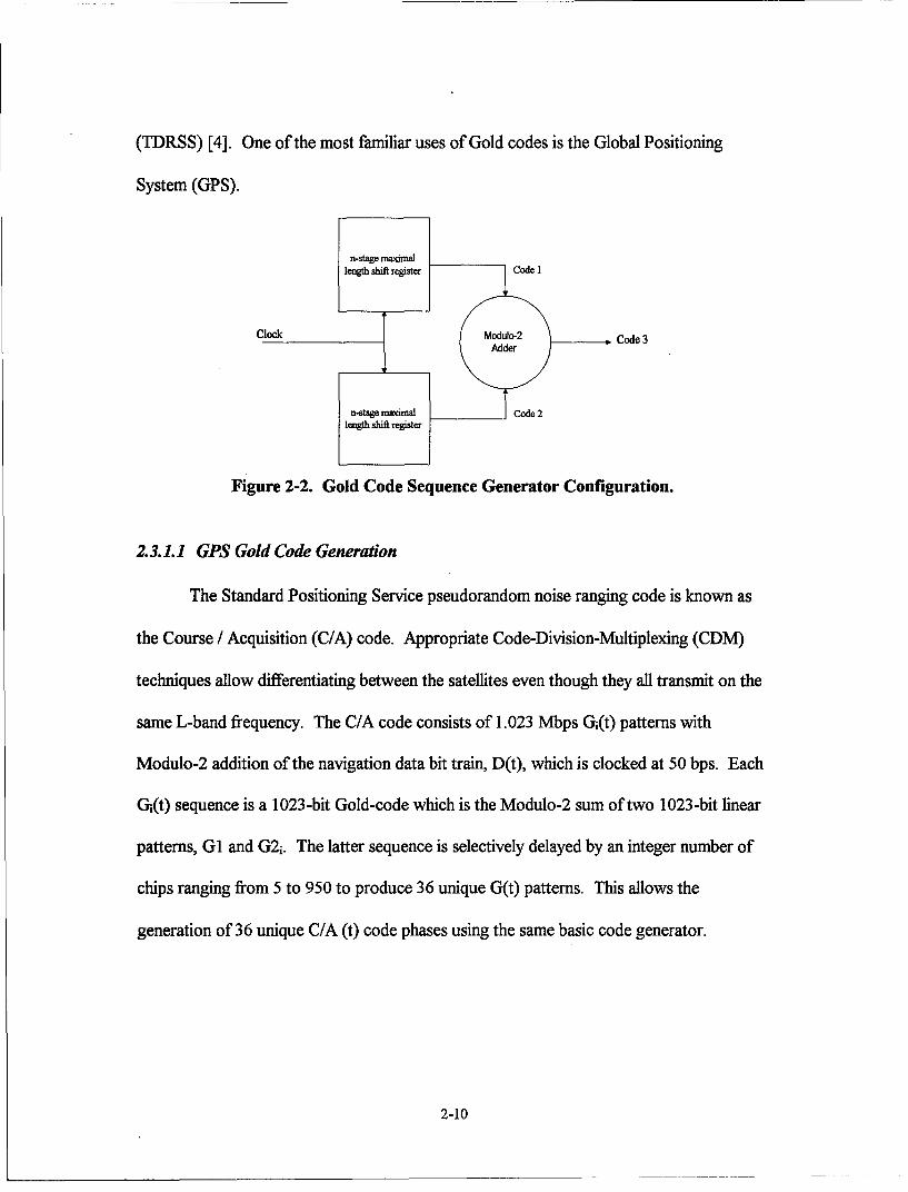
(TDRSS) [4]. One of the most familiar uses of Gold codes is the Global Positioning
System (GPS).
n-stage manimallength shift reptrCd
Clock ouo2Cd3 SCod3s3
Figure 2-2. Gold Code Sequence Generator Configuration.
2.3.1.1 GPS Gold Code Generation
The Standard Positioning Service pseudorandom noise ranging code is known as
the Course / Acquisition (C/A) code. Appropriate Code-Division-Multiplexing (CDM)
techniques allow differentiating between the satellites even though they all transmit on the
same L-band frequency. The C/A code consists of 1.023 Mbps Gi(t) patterns with
Modulo-2 addition of the navigation data bit train, D(t), which is clocked at 50 bps. Each
Gi(t) sequence is a 1023-bit Gold-code which is the Modulo-2 sum of two 1023-bit linear
patterns, GI and G2i. The latter sequence is selectively delayed by an integer number of
chips ranging from 5 to 950 to produce 36 unique G(t) patterns. This allows the
generation of 36 unique C/A (t) code phases using the same basic code generator.
2-10
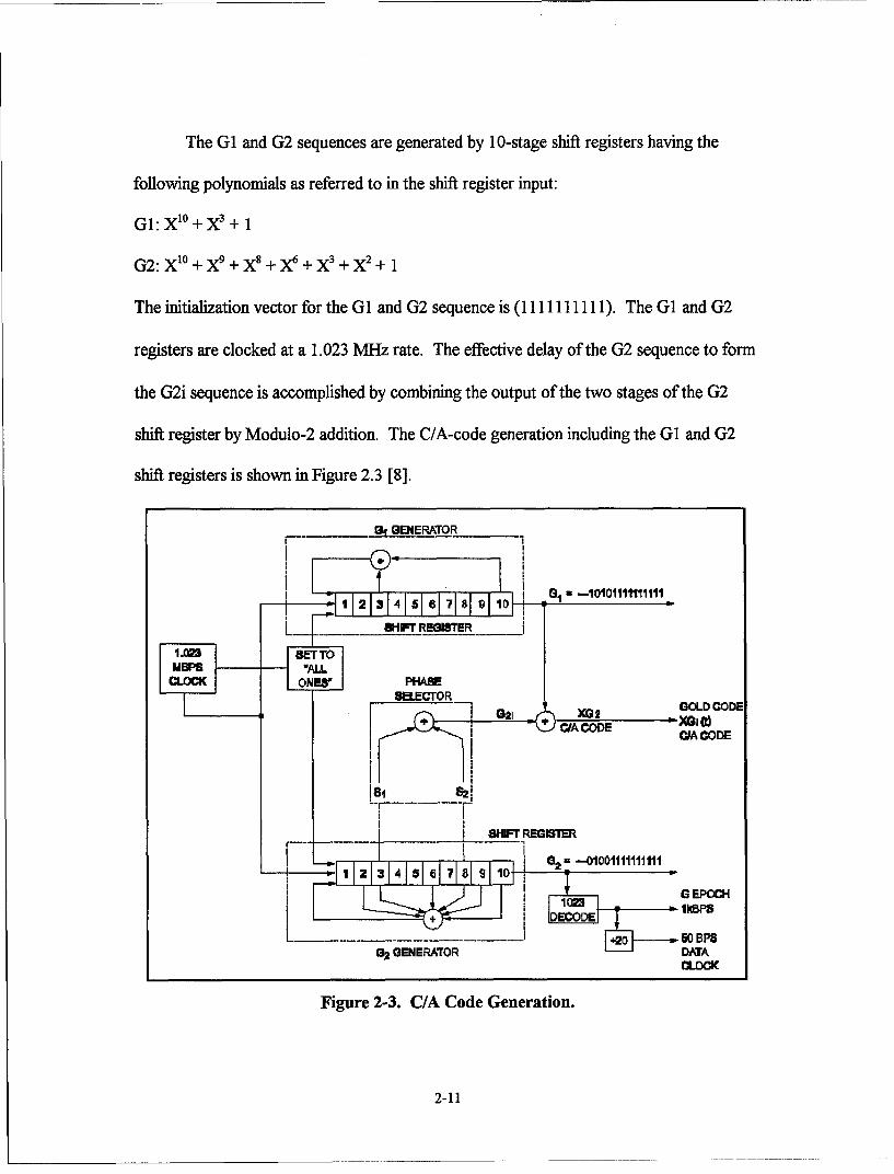
The GI and G2 sequences are generated by 10-stage shift registers having the
following polynomials as referred to in the shift register input:
GI: X'0 + X3 + 1
G2: X1° + X9 + X + + X+ + 1
The initialization vector for the GI and G2 sequence is (1111111111). The GI and G2
registers are clocked at a 1.023 MHz rate. The effective delay of the G2 sequence to form
the G2i sequence is accomplished by combining the output of the two stages of the G2
shift register by Modulo-2 addition. The C/A-code generation including the GI and G2
shift registers is shown in Figure 2.3 [8].
Gg GENERATOR
!01
ý - 2 314151157181 _ 1 __1 1L-_ a-llr RL ____ IGIT
COK PHAS
0 EPOO
S ENERATOR 02 G ODCD
IMAGOL CODODE1
FiurC23.C/A CODE
2 i-1I ~ DCD I 2_-k-0B111111
+2 60BPSt02 GENERATOR DATA
CLOCK
Figure 2-3. C/A Code Generation.
2-11

2.3.2 JPL Ranging Code Generator
The Jet Propulsion Laboratory (JPL) ranging codes are constructed by modulo-2
addition of two or more maximal length linear sequences which are relatively prime to one
another. There are several advantages to such a technique including, 1) very long codes
useful for unambiguous ranging over long ranges are available, 2) the long codes are
generated by a relatively small number of shift register stages, 3) synchronization of a
receiver can be accomplished by separate operations on the component code. This can
greatly reduce the time required for synchronization [1].
Synchronization, via the JPL component codes is accomplished by first cross-
correlating one of the component codes with the composite code. Once this component
code reaches the point of synchronization with its mate, which is embedded in the
composite code, a partial correlation occurs. The partial correlation is then the signal for
the second component code cross-correlation to be initiated which causes the partial
correlation level to be increased. This process continues until all the component codes
making up the overall composite code are individually synchronized with their
counterparts in the received signal. When all are individually synchronized, the correlation
is the same as if the process had simply synchronized the composite code. As an example,
when the component codes are 200, 500 and 1000 chips in length, a separate search
process over these individual lengths (a total of 1700-chips search) can be accomplished
much more rapidly than a search of the composite 108 chips [1].
2-12

Figure 2.4 shows a typical JPL code generator configuration, which has three basic
maximal length shift register generators, each with a different number of stages. This is
identical to the Gold code generator except for the difference in the individual code
lengths.
Shift Register I Code a *db. MM•
(21%l1) bits Add Ad Output
JPL Code
a+b+cClock (2=-1)(21-1)(2"-1) chips
Shift Register 2 Code b(2--1) bits
Shift Register 3 Code c(2P'-1) bits
Figure 2-4. Typical JPL Code Sequence Generator Configuration.
2.3.3 Syncopated-Register Generator
A syncopated-register generator is a technique that multiplexes two or more
slower generators to generate a high-rate sequence. The method is similar to that used in
Gold code sequence generators in that two separate sequences are modulo-2 added to
produce a composite output. The difference lies in that separate clocks, phase shifted by
360/P degrees, each at a rate RIP, where R is the desired output code chip rate and P is
2-13

the number of registers used. Figure 2.5 shows a two-register generator of the syncopated
type. Timing for this code generator is also shown in Figure 2.6. Note the chip rate of
code 1 modulo-2 added to code 2 is twice that of either code 1 or code 2 before their
combination. The overall length of any number of syncopated codes is the product of the
lengths of all the composite codes [1].
Shift Register I CodeI
(2r-1) bits
Cloc T Ad Code 3
(rate M)T (code 1+ code 2)
(2-.1X29-1) chipsShift Register 2 (rateR)
(2"-4) bits Code 2
Clock T + 180 degrees(rate R/2)
Figure 2-5. Syncopated Code Generator.
I CIO& I
aock 2
Code I
Code 2
Cod& 3
Figure 2-6. Syncopated Code Example.
2-14
2.4 Non-Linear Codes
In applications where security is important, it is necessary that the unintended
listener not be able to obtain complete knowledge of the spreading code or encryption
stream being employed. If this code is known, the eavesdropper can decipher or
demodulate the transmitted signal just as the desired receiver. Therefore, the task of
determining the code generator configuration from knowledge of the transmitted signal
should be as difficult as possible. The feedback connections for an n-stage maximal length
sequence can easily be determined from knowledge of 2n successive code symbols [1].
For this reason, m-sequences are never used when a high degree of security is required.
The use of non-linear sequences is one way to increase security. These codes can not be
described by the simple linear recurrence. One way to achieve a non-linear sequence is to
use the output from three linear feedback systems as an address to a
look-up table. This method combines the three output bits to produce one bit based on
the look-up table. Other methods of increasing complexity exist such as using modulo-2
multiplication in addition to modulo-2 addition or using nonlinear feedforward.
2-15

3. System Design
3.1 System Overview
The purpose of this study is to design a pseudorandom code generator for
communication and navigation system applications. The system designed utilizes the
Stanford Telecom STEL-1032, pseudorandom number (PRN) coder [9]. The STEL-1032
PRN coder generates codes using three independent 32-bit register code generators
(CoderO, Coderl, and Coder2). Feedback tap connections for each code generator are
controlled by the MASK Registers content -- any combination of tap connections may be
selected. In this way, each of the three code generators are capable of independently
generating all possible codes with lengths up to 232 - 1 (4,294,967,295) bits. The PN
codes can be started with arbitrary phase by loading the starting phase code into the INIT
Registers. A specific sequence in the code generator registers can be detected and a pulse
generated via a 32-bit magnitude comparator and the values stored in the EPOCH
Registers. The 32-bit COUNT Register is used to set the counter stop point; once
triggered, the counter will run for a number of clock cycles equal to the number stored in
the COUNT Register and then generate a COUNT pulse. The code generators and
counters can be reset on the EPOCH or COUNT pulse. The codes can be made to restart
at this point if desired. In addition to the three independent codes that can be generated,
the outputs of the code generators can be EXORed together, CoderO and Coderl can be
EXORed or all three code generator outputs can be EXORed. The output of code
3-1

combiner is also available both late and early by one-half of a clock cycle relative to the
punctual code (on time). Non-linear codes are generated by means of an internally
programmable look-up table. A block diagram for the STEL-1032 is shown in
Figure 3.1.
K -,,.- --4 0 XORO-2OWE 10XOROI1
ADDR 0-7•- - -40E•.X:•••IMIXOOOESCOMBINER EARLY
OATA 1 PUNCTSLATE
S-41 CGOEC11- • EPOCHO
•4 -COUWJTOLOAO . -- C-01 0 MODQO0StlMO •LDSYNCOSTLD 10 • REFI5S0
SSTSYNC
S~EPOC, H10 COUNTI
S..E1MOD000OiLOAD - LDSYNC1S'TIM1 .... . . • 1 -
CODE2EPOCIW2COUNT2
CLK2C4DOR2 :MODCIOD2"W LDSYNC2
... ...... .. .. .. .. . .. .. ....-. r
Figure 3-1. STEL-1032 Block Diagram.
Each of the three separate coders contain a number of functional blocks, shown in
Figure 3-2. The three coders are completely independent, except for the COUNT and
EPOCH which are interconnected through the coders' control logic. This allows each
coder to be controlled by either of the two other coders.
3-2

STM 'IAOULATOO
STL 0.:R|TENux - CODE
' .. REGISTER DEEOR: "
"N oI • FROMOTHER
Figure 3-2. Individual, Coder Block Diagram.
The STEL- 1032 is programmed by means of the data stored in the registers. Each
of the three independent code generators consists of a complete set of internal registers as
shown in Figure 3-3. The 8-bit data bus is mapped into the 32-bit registers by means of
address inputs ADDR0 through ADDR7 .
3-3
BO 81 B2 INrr REGMSTER t 8
S0 8 2 MASK F,ýGWTER 1B371, 3
PN GENERATOR REGI$TER
3.1.1 0E•L- 03 2 InputsEO PHS so
EPOCH STEL-1032 BInputs
As shown in Figure 3.1, the STEL-1032 has the following inputs: an eight bit
address bus (ADDR), an eight bit data bus (DATA), three coder clocks (CLKO, CLK1,
CLK2), three load pulses (LOADO, LOAD 1, LOAD2), three data lines and a clock for
modulation (STIM0, STIM1, STIM2, and STLD), a chip select (CSN), and a register
write control (WRN). Not shown in Figure 3.1 is the reset (RESET) line.
3-4

3.1.1.1 ADDRo - ADDR7
The PRN Coder has an 8-bit address bus. The addressing scheme is shown in the
tables below where A7 represents the Most Significant Bit (MSB) and AO represents the
Least Significant Bit (LSB)):
Table 3-1. Address bits ADDR 7 - ADDRs.
Coder 0 0 0Coder 0 0 0 1
Coder 2 0 1 0All Coders 0 1 1
Code Combiner 1 0 0
Each independent code generator has the following internally programmable registers
described below.
Table 3-2. Address bits ADDR4 - ADDRo.
MASK 0 0 0 x, x0
MNIT 0 0 1 x1 X0
EPOCH 0 1 0 x1 XoCOUNT 0 1 1 x1 X0
MUX 1 0 0 0 0CTL 1 0 0 0 1
Variables x, and xo are determined according to the table below such that the selected
32-bit register is sequentially loaded 8 bits at a time.
3-5
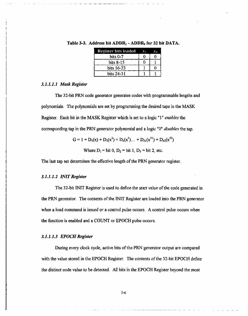
Table 3-3. Address bit ADDRI - ADDRO for 32 bit DATA.
bits 0-7 0_ 0bits 8-15 0 1
bits 16-23 1 0bits 24-31 1 1
3.1.1.1.1 Mask Register
The 32-bit PRN code generator generates codes with programmable lengths and
polynomials. The polynomials are set by programming the desired taps in the MASK
Register. Each bit in the MASK Register which is set to a logic "1" enables the
corresponding tap in the PRN generator polynomial and a logic "0" disables the tap.
G = 1 + DI(x) + D2(x2) + D3(x3)..- + D3 1(x31) + D32(x32)
Where D1 = bit 0, D 2 = bit 1, D3 = bit 2, etc.
The last tap set determines the effective length of the PRN generator register.
3.1.1.1.2 INIT Register
The 32-bit INIT Register is used to define the start value of the code generated in
the PRN generator. The contents of the NIT Register are loaded into the PRN generator
when a load command is issued or a control pulse occurs. A control pulse occurs when
the function is enabled and a COUNT or EPOCH pulse occurs.
3.1.1.1.3 EPOCH Register
During every clock cycle, active bits of the PRN generator output are compared
with the value stored in the EPOCH Register. The contents of the 32-bit EPOCH define
the distinct code value to be detected. All bits in the EPOCH Register beyond the most
3-6
significant feedback tap in the PRN generator must always be set to "0", otherwise a
match will never be detected.
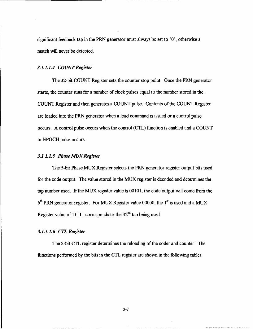
3.1.1.1.4 COUNT Register
The 32-bit COUNT Register sets the counter stop point. Once the PRN generator
starts, the counter runs for a number of clock pulses equal to the number stored in the
COUNT Register and then generates a COUNT pulse. Contents of the COUNT Register
are loaded into the PRN generator when a load command is issued or a control pulse
occurs. A control pulse occurs when the control (CTL) function is enabled and a COUNT
or EPOCH pulse occurs.
3.1.1.1.5 Phase MUX Register
The 5-bit Phase MUX Register selects the PRN generator register output bits used
for the code output. The value stored in the MUX register is decoded and determines the
tap number used. If the MUX register value is 00101, the code output will come from the
6'h PRN generator register. For MUX Register value 00000, the It is used and a MUX
Register value of 11111 corresponds to the 3 2nd tap being used.
3.1.1.1.6 CTL Register
The 8-bit CTL register determines the reloading of the coder and counter. The
functions performed by the bits in the CTL register are shown in the following tables.
3-7

Table 3-4. Control (CTL) Register Bit Functions: (a) B 7-B 6, (b) B5-B 4, (c) B 3-B 2 ,
(d) B1-Bo.
o 06 C tioe dona0 0 Counter is not reloaded on any EPOCH pulse0 1 Counter is reloaded on EPOCHo pulse1 0 Counter is reloaded on EPOCH, pulseo 1 Counter is reloaded on EPOCH2 pulse
(a)
1; 04 Cnrrld onC0 0 Counter is not reloaded on any COUNT pulse0 1 Counter is reloaded on COUNTo pulse1 0 PRCounter is reloaded on COUNT 1 pulse1 1 Counter is reloaded on COUNT 2 pulse(b)
B BF to0 0 PRN generator is not reloaded on any EPOCH pulse0 1 PRN generator is reloaded on EPOCHO0 pulse1 0 PRN generator is reloaded on EPOCH1 pulse1 1 PRN generator is reloaded on EPOCH2 pulse
(c)
0 0 PRN generator is not reloaded on any COUNT pulse0 1 PRN generator is reloaded on COUNT0 pulse1 0 PRN generator is reloaded on COUNT, pulseI I PRN generator is reloaded on COUNT2 pulse
(d)
3.1.1.1.7 Code Combiner Lookup Register
The Code Combiner block shown in Figure 3-1 uses the MODCOD outputs of the
three coders to address a lookup table, shown as Table 3-5, to produce the MIXCOD
output. This allows the production of non-linear codes.
3-8

Table 3-5. Code Combiner Lookup Register Table.
0 O P 0I SI 01 Listei0 0 0 Look-up Register Bit 00 0 1 Look-up Register Bit 10 1 0 Look-up Register Bit 2o 1 1 Look-up Register Bit 31 0 0 Look-up Register Bit 41 0 1 Look-up Register Bit 51 1 0 Look-up Register Bit 61 1 1 Look-up Register Bit 7
3.1.1.2 DATAo-DATA 7
The 8-bit DATA bus writes data into the registers. DATA7 is the most significant
bit (MSB) and DATAo is the least significant bit (LSB). The 8-bit address directs the data
to the proper register.
3.1.1.3 Reset
When the reset input is set low, all of the registers inside the PRN generator are
reset to zero. Normal operation will not commence until an initialization value has been
loaded into the coders from their corresponding INIT registers.
3.1.1.4 CLKo - CLK2
These are the clocks for coder 0 through coder 2 respectively. All operations
occur on the rising edges of the clocks, with the exception of the early and late outputs,
which change on the falling edges of CLKo. The clocks should nominally be square
waves, with a maximum frequency of 30 MHz.
3-9

3.1.1.5 WRN and CSN
The register write control (WRN) is normally high. When this line goes low, data
is written into the register(s) selected by the address lines and latched on the rising edge of
WRN. The Chip Select (CSN) must also be low to enable the data loading.
3.1.1.6 LOADo - LOAD 2
On the rising edge of the clock following the falling edge of a LOAD input, a load
command is issued. This will cause the corresponding coder register and counter to be
loaded with the contents of the corresponding INIT and COUNT Register, respectively.
3.1.1.7 STIMo - STIM 2 and STLD
Data applied to the STIMo - STIM2 inputs is modulo-2 added with the outputs of
the corresponding coder (Codero - Coder2). The data is latched in on the falling edge of
the STLD input.
3.1.2 STEL-1032 Outputs
As shown in Figure 3-1, the STEL-1032 has a total of 25 outputs. The code
combiner outputs XORO1, XOR012, MIXCOD, EARLY, LATE, and PUNCT. Each
coder outputs a CODE, EPOCH, COUNT, MODCOD, LDSYNC, and REF15. An
STSYNC signal comes from CoderO.
3-10

3.1.2.1 CODEo - CODE 2
The CODE0 - CODE2 outputs are the outputs of the Codero - Coder2. The register
bit in the coder from which the output is derived is set by the Phase MUX.
3.1.2.2 MODCODo - MODCOD 2
The MODCOD0 - MODCOD 2 outputs are the CODE0 - CODE2 signals after
modulation by the STM 0 - STIM2 inputs. The register bit in the coder from which the
output is derived is set by the Phase MUX.
3.1.2.3 LDSYNCo- LDSYNC2
The LoaDSNYC output goes low for one clock cycle after the contents of the
corresponding INIT register been loaded into the corresponding coder. This pulse
indicates the clock cycle in which the coder value is identical to that of the INIT register.
3.1.2.4 REF15o - REF152
The REF15 0 - REF152 outputs are the reference codes derived from the taps
number 15 of the corresponding coder. These outputs will be identical to the
corresponding CODEo- CODE2 outputs when the data stored in the corresponding Phase
MUX is 01111 (tap number 15).
3.1.2.5 EPOCHo - EPOCH2
The EPOCHo - EPOCH2 outputs are normally high and go low whenever the
corresponding coder code is equal to the code stored in the EPOCH Register for that
coder. This condition will not be detected and the EPOCH output will not go low if this
3-11
condition occurs within 2 clock cycles of the rising edge on the corresponding EPOCH
input.
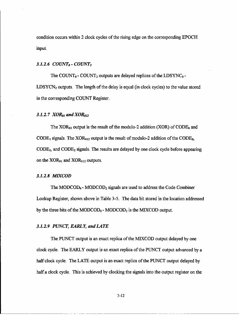
3.1.2.6 COUNTo- COUNT 2
The COUNTo - COUNT2 outputs are delayed replicas of the LDSYNCO -
LDSYCN 2 outputs. The length of the delay is equal (in clock cycles) to the value stored
in the corresponding COUNT Register.
3.1.2. 7 XOR01 and XOR0 12
The XOR01 output is the result of the modulo-2 addition (XOR) of CODEo and
CODE, signals. The XOR01 2 output is the result of modulo-2 addition of the CODE0 ,
CODE,, and CODE2 signals. The results are delayed by one clock cycle before appearing
on the XOR01 and XOR0 12 outputs.
3.1.2.8 MIXCOD
The MODCOD0 - MODCOD 2 signals are used to address the Code Combiner
Lookup Register, shown above in Table 3-5. The data bit stored in the location addressed
by the three bits of the MODCOD0 - MODCOD2 is the MIXCOD output.
3.1.2.9 PUNCT, EARLY, and LATE
The PUNCT output is an exact replica of the MIXCOD output delayed by one
clock cycle. The EARLY output is an exact replica of the PUNCT output advanced by a
half clock cycle. The LATE output is an exact replica of the PUNCT output delayed by
half a clock cycle. This is achieved by clocking the signals into the output register on the
3-12
falling edges of CLKo. In order to make the advance and delay exactly half a clock cycle,
the duty cycle of CLKo must be exactly 50%.
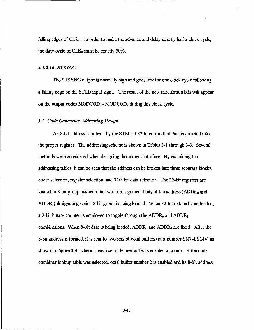
3.1.2.10 STSYNC
The STSYNC output is normally high and goes low for one clock cycle following
a falling edge on the STLD input signal. The result of the new modulation bits will appear
on the output codes MODCOD0 - MODCOD 2 during this clock cycle.
3.2 Code Generator Addressing Design
An 8-bit address is utilized by the STEL- 1032 to ensure that data is directed into
the proper register. The addressing scheme is shown in Tables 3-1 through 3-3. Several
methods were considered when designing the address interface. By examining the
addressing tables, it can be seen that the address can be broken into three separate blocks,
coder selection, register selection, and 32/8 bit data selection. The 32-bit registers are
loaded in 8-bit groupings with the two least significant bits of the address (ADDRo and
ADDR1) designating which 8-bit group is being loaded. When 32-bit data is being loaded,
a 2-bit binary counter is employed to toggle through the ADDRO and ADDR1
combinations. When 8-bit data is being loaded, ADDRo and ADDR1 are fixed. After the
8-bit address is formed, it is sent to two sets of octal buffers (part number SN74LS244) as
shown in Figure 3-4, where in each set only one buffer is enabled at a time. If the code
combiner lookup table was selected, octal buffer number 2 is enabled and its 8-bit address
3-13

is passed on; otherwise octal buffer number 1 is enabled and the formed address is passed
on to octal buffer number 3. When the code generator is operating in manual entry mode
the address is passed on to the STEL-1032 via octal buffer number 3. If external
programming is being performed, octal buffer number 4 passes the address. The design
of the coder selector, register selector and 32/8 bit data selection is descrided below.
Coder SelectorA7, A6, A5
Octal Buffer 8 - sm Octal BufferN
Number 1 8 Address Lines Number 3 8 Address Lines
(mvated Externali Address _try)
R4STEL-1032
SelectorA4 ,A3, A2
L•mfonSelector
Al, A0 Octal Buffer -_-.J\, Octal BufferNumber 2_ Number 4(Code Combier
fixe add-~) (copu- ter ey)
External Address Input
Figure 3-4. Address Block Diagram.
3-14

3.2.1 Coder Selector Design
As shown in Table 3-1, the coder selector has five options and occupies the three
most significant bits of the address (ADDR7 - ADDR5). The coder selector takes one of
five choices and outputs the three bits corresponding to the address of the coder selected.
A shown in Table 3-6, an 8-line to 3-line priority encoder (part no. SN54148) produces a
3-bit output based on the location of the first low level logic encounter. Figure 3-5 shows
how this TTL device was used in the coder selector design.
Table 3-6. 8-Line to 3-Line Priority Encoder Function Table.
U..NPUT OUTPUTSo 1 2 3 4 5 6 7 A2 Al AOH H H H H H HH H H Hx x x x x x x L L L Lx x x x xx L H L L Hx xx x x L H H L H Lx x x x L H H H L H Hx x x L H H H H H L Lx x L H H H H H H L Hx L H H H H H H H H LL H H H H H H H H H H
••!i@I •5 volts
8-Line to 3-LineCodr2Priority Encoder -- A6
CAI Cders- A5
OC=d Combiner
Figure 3-5. Coder Selector Design.
3-15
Using a 2.2KM resistor as a pull-up resistor, the input lines remain a logic high
until selected. The coder selector switch is a push button switch tied to ground which
allows one selection at a time. By selecting a coder, the corresponding line is grounded
and a logic low appears on the input line and ADDR7 - ADDR5 are output from the
encoder in accordance with Table 3-6.
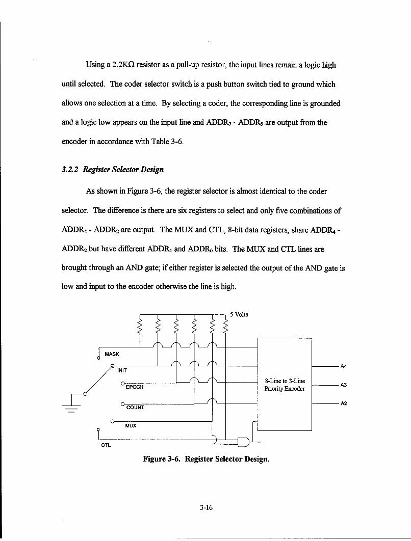
3.2.2 Register Selector Design
As shown in Figure 3-6, the register selector is almost identical to the coder
selector. The difference is there are six registers to select and only five combinations of
ADDR4 - ADDR 2 are output. The MUX and CTL, 8-bit data registers, share ADDR4 -
ADDR2 but have different ADDR, and ADDRo bits. The MUX and CTL lines are
brought through an AND gate; if either register is selected the output of the AND gate is
low and input to the encoder otherwise the line is high.
5 Volts
A4
0 EPO8-Line to 3-LinePriority Encoder
u..._A2zo ~COUNT A
CTL
Figure 3-6. Register Selector Design.
3-16

3.2.3 32 or 8 bit Data Address
Since the STEL-1032 has an 8-bit address and data bus, the 32-bit registers must
be loaded in four 8-bit blocks, each with a different address. As shown in Table 3-3, the
two Least Significant Bits (LSBs) of the address, ADDR1 and ADDRo, direct the 32-bit
data into the proper location in the register. In the 8-bit registers, ADDR1 and ADDRo are
fixed. Figure 3-7 shows the design for generating the ADDR1 and ADDRO bit required for
32-bit data entry. With the load switch depressed, the reset on the clock (part number
555) goes high and the clock begins to run. Resistor and capacitor values are chosen to
produce a high-to-low square wave clock with a frequency of about 1 Hz. This allows the
address and data to stabilize before being loaded in to the PRN coder. Waveform timing
is presented in Section 3.4. The clock output increments the binary counter and triggers
the one-shot multivibrators used to load the registers. The clock is controlled by the reset
input; it continues to run as long as the reset line is held high. Because it was desirable to
have the clock run for 4 cycles and toggle through the various ADDR1 and ADDRo
combinations, several logic gates are employed to control clock operation. The
following conditions must simultaneously occur to force the reset line and stop the clock:
a) both A1 and Ao from the binary counter go high, b) the clock transitions to a low state,
and c) the load switch is released.
3-17

5V 5V
To LTo
3 13 AData Buffer6 Biar Enable Logic
A,; -- v AO
Clock 3 Cok . 6 6
-T IluF
.01 uF
Figure 3-7. Clock and Counter Design.
As shown in Figure 3-8, when 32-bit data is being loaded, address bits ADDR, and
ADDRo equal the counter output; when the MUX or CTL Registers are being loaded,
ADDR1 and ADDRo are fixed.
Al
A0Enbe Tri-l
ADDR7 EnADDR 1
AADD R-ADDR0
MUX
Figure 3-8. ADDR1 and ADDRO Generation.
3-18

3.3 Code Generator Data Entry Design
Since the STEL-1032 has eight data line inputs, several options were considered
for data entry. As discussed in the previous sections, the entire 32 bits of data may be
entered on the thumbwheel switches but through TTL logic gates, only eight bits are
loaded into the registers at a time. Figure 3-9 shows an overview of the data entry design.
Data is entered via 11 octal thumbwheel switches. The 33 data lines are routed to three
different banks of octal buffers. The first set of four octal buffers are connected to the 32
Least Significant Bits (LSB) of the thumbwheel switches for entering data into the
following 32-bit registers: INT, EPOCH, and COUNT. The second set of buffers contains
a single octal buffer connected to the LSB on each of the eight right most thumbwheel
switches. This allows the 8-bit data to be entered in binary format. The third set contains
four octal buffers connected to the 32 Most Significant Bits (MSB) of the 11 thumbwheel
switches. This allows data to be entered into the MASK Register.
32 Daa 4 Octal Buffers Manual Entry
F2Dt igues 3-. ata Entr esig Blc Diagram. e
NIT, EPOCH S-Data Buffer9and COUNT) I 3
BankOf Single
I I 8ains Octal Buffer 8Dt ie Computer EntryOctal stt• (Co~de Con-biner, st Data Buffer •
Thumbwheel MUX, C'R,)/Switches/
N Bank of
321N"tai~nes 4 Octal Buffer's 8 DX"Lin"(MASK)
Figure 3-9. Data Entry Design Block Diagram.
3-19

3.3.1 Data Buffer Enable Design
The octal buffers are tni-state devices with output characteristics as shown in
Table 3-7. To ensure data is properly loaded into the desired register two things must
occur, the correct buffer must be enabled and the proper address must be present.
Table 3-7. Tri-State Octal Buffer Outputs.
1Fnble hIftitS OutputL L LL H HH X I-Z
As shown in Figure 3-10, TTL logic and the binary counter outputs used to set
ADDR1 and ADDRO lines ensure the octal buffers are enabled in the proper order. For
the data to be correctly entered, only one buffer enable can be low at any time; logic gates
prevent two or more buffers from being enabled at one time. The Code Combiner and
MUX / CTL lines are normally low but if one is chosen the line transitions high and passes
through the OR gate. The high level inverts and the low output level enters the AND
gates keeping them low and disabling the 32-bit buffers. When 32-bit data is loaded,
through the use of inverters and AND gates the binary counter output enables one buffer
for each count. The OR gates in the 32-bit buffer enables are controlled by the MASK
selection. If the MASK is selected, the line to the MASK buffer OR gates is low and its
buffers are enabled by the counter otherwise it remains in a high state and the OR gate
output remains in a high state disabling the buffers.
3-20

INT
COUNT
SCo mbiner A] E ff 0
Buffer I
Buffer 3
Figure 3-10. Data Buffer Enabling Design.
3.3.2 Data Entry Format
Data enters via 11 octal thumbwheel switches with the LSB occupying the
rightmost position. Since data is loaded into registers with the LSB first, data is set on the
rightmost thumbwheel and work to the left. The 8-bit data (Code Combiner, MUX, and
CTL) is entered in binary format on the eight rightmost thumbwheels with the LSB on the
right. The 32-bit data is entered in octal format. The binary-to-otal conversion is
accomplished by grouping the binary bits into groups of three starting with the LSB and
working toward the MSB. A group of three bits are converted to their octal equivalent
and entered on the thumbwheel switches starting on the right with the least significant
3-21

octal number. For example, if the initial fill of a 17 stage register was to be 1 0 11 0 0 1 1
0 0 0 1 0 11 0 1 with the last bit to be entered into the B0 register, the thumbwheels
would be set at 0 0 0 0 2 6 3 0 5 5. Octal thumbwheels were chosen because tables are
readily available with the octal representation of primitive polynomials that produce
maximal length sequences. Appendix A includes a partial list these octal representations.
3.4 Code Generator Data Loading
To load data into the STEL-1032, sequential Chip Select (CSN) and Write Enable
(WRN) pulses must occur following data and address stabilization. A low level CSN
input enables the loading of data via the data lines and when the WRN line is low data is
written into the register(s) selected by the address lines; the data is latched on the rising
edge of the WRN pulse. Figure 3-11 shows the how these pulse are created. Dual non-
retriggerable one-shot multivibrators (part number 74LS221) are used to generate the
necessary pulses.
5V
Clock B8
A
5V
CCB a
A S
5V 5Vj
Figure 3-11. Load Pulse Design.
3-22

As discussed in Section 3.3, after the LOAD button is depressed the clock is
triggered incrementing the counter that enables the buffers and sets ADDR1 and ADDRO.
The clock pulse also triggers the first multivibrator which serves as a delay to allow the
address and data to stabilize. On the falling edge of the delay pulse, the second
multivibrator is triggered producing the CSN pulse. The falling edge of the CSN pulse
triggers a third multivibrator, producing the WRN pulse. The total delay between the
CSN and WRN pulses is the internal delay from the multivibrator. The pulse width are
controlled by the proper selection of resistors and capacitors. Figure 3-12 shows the
relationship of these pulses.
Clock
Delay
CSN
WRN
0 Time
Figure 3-12. Data Loading Pulse Comparison.
After data is loaded into the registers, a LOAD pulse is necessary to fill the PRN
Generator with values stored in the INIT register. On the rising edge of the clock pulse
3-23

following the falling edge of a LOAD pulse, the PRN Generator register and counter
register are filled with the contents of the INIT and COUNT registers, respectively. A
momentary push button switch is connected to a multivibrator to generate the LOAD
pulse.
3.5 Other Code Generator Inputs
There are eight other inputs available on the code generator; a reset, three clocks,
three external data lines and a data clock. The code generator is reset via a momentary
push button switch which sets all register contents inside the PRN coder to zero. The
three PRN coders are clocked independently (clock inputs are provided via a BNC
connector on the front of the code generator). Data applied to the STIM inputs via BNC
connectors are modulo-2 added with the outputs of the corresponding PRN coder. Data is
latched on the falling edge of the signal on the BNC connector to the STLD input.
3.6 Code Generator Outputs
The code generator has a total of 25 outputs, the 15 waveforms and 10 pulses
previously described in section 3.1.2. Each output is connected as shown in Figure 3-13.
A 50nf quad 2-input NOR gate line driver (SN74128) was chosen to interface between
the code generator and front panel. The output of the STEL-1032 is inverted before
entering the line driver inputs since it also inverts the output. The result is a waveform or
pulse of proper orientation.
3-24
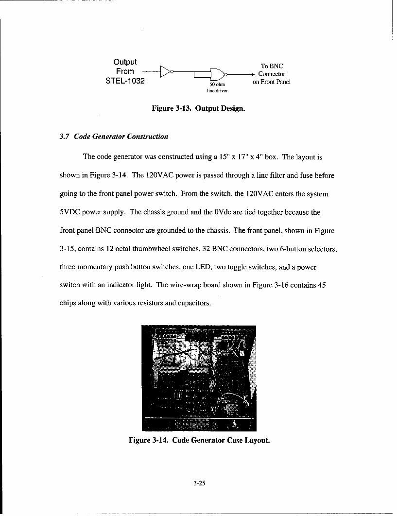
Output To BNCFrom -- [->o Connector
STEL-1032 50 ohm on Front Panelline driver
Figure 3-13. Output Design.
3.7 Code Generator Construction
The code generator was constructed using a 15" x 17" x 4" box. The layout is
shown in Figure 3-14. The 120VAC power is passed through a line filter and fuse before
going to the front panel power switch. From the switch, the 120VAC enters the system
5VDC power supply. The chassis ground and the OVdc are tied together because the
front panel BNC connector are grounded to the chassis. The front panel, shown in Figure
3-15, contains 12 octal thumbwheel switches, 32 BNC connectors, two 6-button selectors,
three momentary push button switches, one LED, two toggle switches, and a power
switch with an indicator light. The wire-wrap board shown in Figure 3-16 contains 45
chips along with various resistors and capacitors.
Figure 3-14. Code Generator Case Layout.
3-25

Figure 3-15. Code Generator Front Panel.
Figure 3-16. Code Generator Circuit Board.
3-26
3.8 Code Generator System Design Summary
The interface design consists of several TTL logic gates. Programming the code
generator is accomplished via the front panel. Depressing the LOAD button causes the
data entered on the thumbwheel switches to be loaded into the STEL-1032 in accordance
the coder(s) and register(s) selected. With construction of the code generator complete,
the outputs presented in Section 3.1.2 are authenticated in Chapter 4.
3-27

4. Code Generator Evaluation
4.1 Code Generator Loading Pulses
Before code generation begins, initialization data is loaded into the STEL-1032
Pseudorandom Number (PRN) coder registers. Data is loaded into the coder registers
using sequential Chip Select (CSN) and Write Enable (WRN) pulses which occur
following data and address stabilization. As discussed in Section 3.2.3, a clock circuit
increments a counter to enable the data buffer and establish the address. A set of one-shot
multivibrators are sequentially triggered to generate the CSN and WRN pulses. The
following equation is used to determine the proper resistor and capacitor values to obtain
the desired high-to-low square wave clock period. Period = ln(2) * (RA+ 2R1) * C. For
RA equal to 750 KM, RB equal to 360 KM, and C equal to 1 gF, the period is 1.019
seconds or .98 Hz. The actual data loading clock circuit output is shown in Figure 4-1.
C1 Freq833.40mHz
Cl Amp..... -.... ....... = .... ...... 4 2M
.. . .. .. . .. ... ." . . . . . . . . .. . . . . ... . m s
I[ .. ..I I. . . .. . I.. . . •.... ;.... . . . h... .... .. . . . . .- . .
Figure 4-1. Code Generator Data Loading Clock.
4-1

As shown, the period of the actual clock is 1.2 seconds. The rising edge of the data
loading clock triggers a one-shot multivibrator, the resultant output pulse serves as a delay
which triggers another one-shot multivibrator, generating a CSN pulse. The CSN pulse
then triggers another one-shot multivibrator, producing the WRN pulse. Figure 4-2 shows
the actual pulses for loading the data. The data loading clock is displayed as Reference
number 1 (RI), the CSN pulse is on Channel 1 (1), and the WRN pulse is on Channel 2
(2). The delay between the rising edge of the clock and the CSN pulse allows the
STEL-1032 data and address inputs to stabilize prior to loading. The delay time, CSN
and WRN pulse widths are determined by the following equation. Width = ln(2) * R *C.
For implementation, 150 KO resistors are used. A delay capacitance of 1 p.F, CSN
capacitance of 4.7 pF, and WRN capacitance of 2.2 gxF are used to provide a delay of 104
milliseconds, a CSN pulse width of 487 milliseconds and a WRN pulse width of 229
milliseconds, respectively.
C1 -Width414.Oms
Low signalM . . . .amplitude
C2 -width-4 1 OM ... 240.Oms
Ref l4C1 MY112. Oms
* . .Low signal. . ... ...... .... ... ... ... ... am plitude
Figure 4-2. Data Loading Clock, CSN, and WRN Pulses.
4-2

4.2 Coder Outputs
The STEL-1032 code generator consists of four major components, three
independent coders (CoderO, Coderl, and Coder2) and a code combiner (See Figure 3-1).
The results presented in this section are derived from tests performed on CoderO and are
representative of outputs for all three coders. The following outputs are authenticated:
pseudorandom code, LDSYNC, COUNT, EPOCH, REF15, and MODCOD. Each test is
performed using the 3-stage linear feedback shift register configuration shown in
Figure 4-3.
x x 2 X3Output
Figure 4-3. Test Linear Feedback Shift Register.
The linear feedback shift register of Figure 4-3 may be represented by a polynomial
of the form X3 + X + 1; the binary representation is (1 0 1 1) and octal representation
which is set on the thumbwheel switches is [1 3]. The register contents following each
clock cycle are shown in Table 4-1 where all of the registers are initially filled with a '1'.
4-3
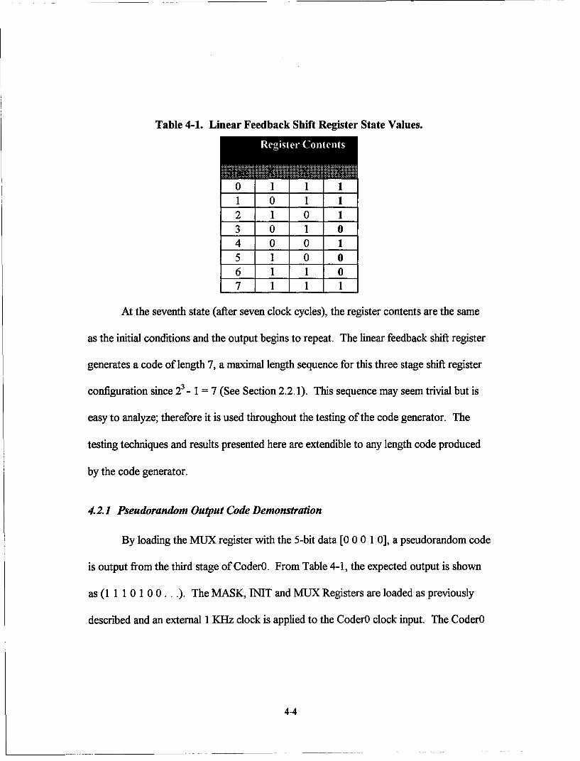
Table 4-1. Linear Feedback Shift Register State Values.
11 -
3 0 1 0
4 0 0 15 1 0 06 1 1 07 1 1 1
At the seventh state (after seven clock cycles), the register contents are the same
as the initial conditions and the output begins to repeat. The linear feedback shift register
generates a code of length 7, a maximal length sequence for this three stage shift register
configuration since 23 - 1 = 7 (See Section 2.2.1). This sequence may seem trivial but is
easy to analyze; therefore it is used throughout the testing of the code generator. The
testing techniques and results presented here are extendible to any length code produced
by the code generator.
4.2.1 Pseudorandom Output Code Demonstration
By loading the MUX register with the 5-bit data [0 0 0 1 0], a pseudorandom code
is output from the third stage of CoderO. From Table 4-1, the expected output is shown
as (11 1 0 1 0 0... ). The MASK, INIT and MUX Registers are loaded as previously
described and an external 1 KHz clock is applied to the CoderO clock input. The CoderO
4-4

pseudorandom output, CODEO, is shown on Channel 1 along with the coder input clock
on Channel 2 in Figure 4-4.
... . . . . . . . . ... . . ... . . ... . . . . . . . . . . . . . . .. .. . . . . . . . . . . . . . . . .
.. .. . . . . . . . . . . . .. . . . . .
. . . . . I. .. .
2 . j . .1- * -- 1*L ý
Figure 4-4. CODEO and Input Clock.
The code appears as expected but it is difficult to determine the period of the code
from Figure 4-4. By changing the time scale as shown in Figure 4-5, the length of the
code is easily determined as 7, i.e., 7 input clock cycles per code period.
Figure 4-5. Multiple Periods of CODEO and Clock Pulse.
4-5

4.2.2 LDSYNC Pulse Output Demonstration
After the contents of the INIT register are first loaded into the coder, the "Load
Synchronization" LDSYNC output is expected to go low for one clock cycle. Shown in
Figure 4-6, CODEO is displayed on Channel 1 and the expected LDSYNC pulse is shown
on Channel 2.
S.. . . . . . . . . . . . . . . . . . . . . . . . 't.... . . . . . . . . . . . . . . . . . . . . . . ..
S. . . j . . . . . .
.. ... . ....... . .... ... .. . .. ... .. .. . ..... ...
...... ..k ......... .. .. .. . ..... ..... .... . ......T.: " : 4- : *
Figure 4-6. CODEO and LDSYNC Pulse.
4.2.3 COUNT Pulse Output Demonstration
The COUNT pulse is a delayed replica of the LDSYNC. The amount of delay is
determined by the value loaded into the count register. By loading the count register with
[8], a low LDSYNC pulse is expected to occur on the eighth clock cycle, the first bit of
the second period in CODEO. As shown in Figure 4-7, the COUNT pulse output appears
as expected on the lower trace of the display.
4-6

S.. . . . !. . . . !. . . . . . . !. . . . ±.. . .. . . . . . .. !. . . .. ! . . . . !. . . ..
. . . . . . . . .. . . .. ..
Figure 4-7. CODEO and COUNT Pulse.
4.2.4 EPOCH Pulse Output Demonstration
The EPOCH output is normally high and goes low whenever the coder register
contents are equal to the value set in the EPOCH register. Loading [4] in the EPOCH
register represents stage X3 = 1, X2 = 0, and X, = 0. From Table 4-1, this condition
occurs at state 4, the fifth output bit. Figure 4-8 shows the resultant EPOCH pulse output
relative to CODE0 on traces 2 and 1, respectively.
S . . .... ..
S.........
. . . .
Figure 4-8. CODEO and EPOCH Pulse.
4-7

4.2. 5 Pseudorandom Code at REF15 Demonstration
The REF15 output is the pseudorandom code taken from tap number 15 ( the 16th
tap, taps number from 0 to 31 per Figure 3.3). The output is identical to the CODE
output if the MUX is loaded with ( 0 1 1 1 1) which corresponds to tap number 15.
Figure 4-9 shows the CODEO (third tap) on Channel 1 and the REF 15 output on
Channel 2. The REF15 output remains in a low state for thirteen clock cycles which
means the REF15 output is thirteen stages from the CODEO (tap number 2) output. This
confirms that loading the MUX with a binary fifteen (0 1 1 1 1), CODEO output taken
from tap number 15, CODEO and REF15 outputs are identical. This is contrary to
information provided by the vendor. [9]
S.. . . . . . . . . . . . . . . . . . . . . . . . . . . . . . . . . . . . . . . . . . . . . . . ..-
".1"
.. . .. " . . . . .• .. 2.d. _ . . . . . . . , . . . . . . . .
Figure 4-9. CODEO at Tap Number 2 and REF15.
4-8

4.2.6 MODCOD Output Waveform Demonstration
The MODCOD is the CODE signal modulated by the STIM inputs and delayed by
one clock cycle before appearing on the output. Figure 4-10 shows CODEO and the
MODCOD when the STIM input is '0'.
.. . .. . . . . . . .. !. . . . . . . ... . . . . . . . . . . . . . . . . . . .
... . . .: . . . .: . . . . . . . . .: . . . .t ' . . . . . . . . . . . . .: . . . . . . .
14 . . P9 -
.. . . ....... ... .. .... .
............. .. . . . .
.. . . . . . . . . . . .. I+ . . . .
t
Figure 4-10. CODEO and MODCOD.
4.3 Code Combiner Outputs
The code combiner is capable of producing the following output codes: XORO1,
XOR012, MIXCODE, EARLY, PUNCT, and LATE. The following tests are performed
using the linear feedback shift register configuration of Figure 4-3 for CoderO and the
configuration of Figure 4-11 for CoderI and Coder 2. It is easily verified that the 3-stage
configuration of Figure 4-11 provides a maximal length sequence.
4-9

P. xi 2 X3output
Figure 4-11. Test Linear Feedback Shift Register (Coderl and Coder2).
The linear feedback shift register of Figure 4-11 may be represented by the polynomial
X0 + )e + 1; its binary representation is (11 0 1) with an octal representation loaded into
the MASK register of [1 5]. The register contents are shown in Table 4-2 where all
registers are initially filled with a '1'. This linear feedback shift register along with the shift
register of section 4.2 are used in this section for testing combined code outputs.
Table 4-2. Linear Feedback Shift Register State Values.
4-10
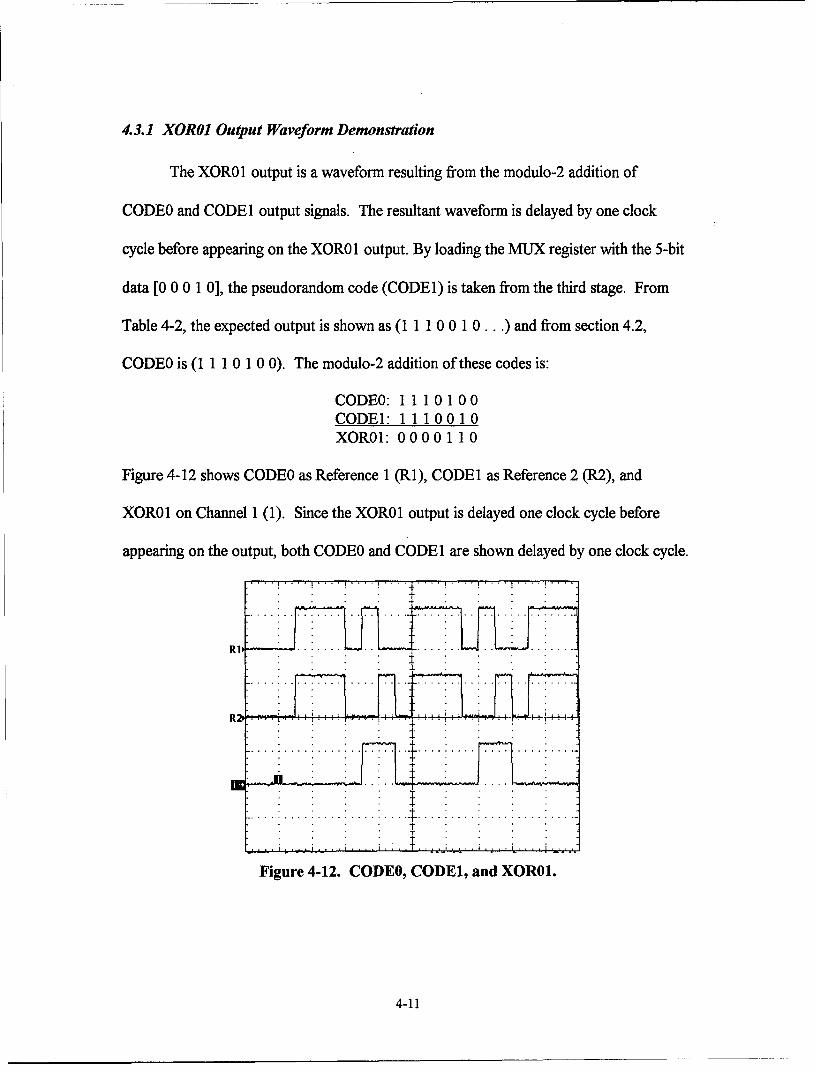
4.3.1 XOROI Output Waveform Demonstration
The XORO1 output is a waveform resulting from the modulo-2 addition of
CODEO and CODE 1 output signals. The resultant waveform is delayed by one clock
cycle before appearing on the XOR01 output. By loading the MUX register with the 5-bit
data [0 0 0 1 0], the pseudorandom code (CODE 1) is taken from the third stage. From
Table 4-2, the expected output is shown as (11 1 0 0 1 0...) and from section 4.2,
CODEO is (11 1 0 1 0 0). The modulo-2 addition of these codes is:
CODEO:1 1 10100CODEI: 11 10010XORO1: 00001 10
Figure 4-12 shows CODEO as Reference 1 (RI), CODE1 as Reference 2 (R2), and
XORO1 on Channel 1 (1). Since the XOR01 output is delayed one clock cycle before
appearing on the output, both CODEO and CODE 1 are shown delayed by one clock cycle.
. . . ! . . . . . ! . . ... . •.. . . !.. . . !.. . . . . . . !.. . .
. . . . . . . . .
R2o
. . . . . . . . . .
.. . . . .. . . . . . . . . . . . . . . . . . . . .
Figure 4-12. CODEO, CODE1, and XOR01.
4-11

Since CODEO and CODE I are maximal length sequences, the modulo-2 addition
of them is a Gold code of the same length but nonmaximal. The seven bit sequence could
also be generated using a single linear feedback shift register with a generator polynomial
of X6 + Xý + X' + Xý + X2 + X + 1, the modulo-2 multiplication of the two generator
polynomials. Since the 6 stage linear feedback shift register is nonmaximal, the initial
conditions produce outputs of varied length. Using the first six bits of the Gold code
generated (0 0 0 0 1 1) as the initial conditions in the 6 stage register, the pseudorandom
code is identical to the Gold code. Figure 4-13 shows the Gold code, and the nonmaximal
pseudorandom code generated using Coder2.
S.. . . i. . . .. i. . . .. ;. . . .. . . . . . . . . . . i . . . . ! . .
S... . . :...... . . . ...... Z. . . .Z. . . .
Z&
S.. ... .... . . . . . . . .. . .. . . . . ..
Figure 4-13. Gold Code and Nonmaximal Pseudorandom Code.
By changing the initial conditions in Coderl (a phase shift), a different Gold code
is produced. With an initial condition ofX, = 1, X2 = 0, and X3 = 0, the expected Gold
code is
CODE0: 1110100CODEI: 0010111
Gold code: 1100011
4-12

The new Gold code along with CODEO and CODE1 are shown in Figure 4-14.
" .. .. . . . . : . . . .• . . . . : . . . .).. . ..
. .. . . . . .. . . . .
• "2 .. .. . . . . . . . .. . . . . . . . . . .., ,
Figure 4-14. CODEO, CODE1, and Gold Code.
4.3.2 XORO12 Output Waveform Demonstration
The XOR012 output is the result of the modulo-2 addition of CODEO, CODE 1,
and CODE2. With CoderO and Coderl unchanged from the previous demonstration,
Coder2 is configured the same as Coderl except the initial conditions are (1 11). The
expected code is given as:
CODEO: 1110100CODEL: 00 10 111CODE2:1 1 10010
XOR012: 0010001
The generator outputs are shown in Figure 4-15 with CODEO through CODE2 as
Reference 1 through 3, respectively, and XOR012 on Channel 1.
4-13

Figure 4-15. CODE., CODE1, CODE2, and XOR012.
4.3.3 MIXCOD Output Waveform Demonstration
The MODCODo - MODCOD2 signals address the 8-bit code programmed into the
code combiner lookup register. With the STIM0 - STLM2 inputs held low, the MODCODo
- MODCOD 2 signals are a one cycle delay of CODE0 - CODE2 respectively. The
MODCOD signals are:
MODCOD0:1 1110100MODCOD1 : 0010111MODCOD9 : 1110010
Look-up Register Address Bit: 5 57 0 362
The code combiner lookup register is loaded as shown in Table 4-3.
4-14

Table 4-3. Example Look-up Table.
0 01 1
2 03 14 15 06 1
7 1
Using MODCOD0 - MODCOD2 to address Table 4-3, the predicted MIXCOD is
(0 0 1 0 11 0). Figure 4-16 shows the MIXCOD output waveform in addition to
MODCODo - MODCOD 2 as Reference waveforms.
S.. . ! . . . . .!.. . . !.. . . . . . . . . . . •.. . . j.. . .. .. .
Figure 4-16. MODCOD 0 - MODCOD 2 and MIXCOD.
4.3.4 PUNCT, EARLY, and LATE Output Waveform Demonstration
The PUNCT output is an exact replica of the MIXCOD delayed by one clock
cycle; as shown in Figure 4-17. The EARLY output is an exact replica of the PUNCT
4-15

output advanced by half a clock cycle as shown Figure 4-18. The LATE output is an
exact replica of the PUNCT output delayed by half a clock cycle and is shown in
Figure 4-19.
.. .. . . . . *.. . . .*... ... . . . . . . . .S.. . .. ! . . . . ! . . . . !. . . .. ! . . . . .]. . . . . ! . . . . ! . . . . ! . . . . . . . ..
..... †††..†.††..... ...... ... ...
Figure~~ 447 ICO n U TOtus
....... ...... .... ...
.. . . . . . . . . . . . . . . . . .. . . .. .i . . . . . . . . . . . . . . . . . . . . . . . ...
T
1-;~~~~~ ~~ .4~ 4 .. . . * .. .*4*4*4 .4*~~ .... 4
Figure 4-17. MIXCOD) and P1JNCT Outputs.
J ... . . .
Figure 4-18. PUNCT and EARLY Outputs.
4-16

S.. . .. !. . . .. !. . . .. !. . . .. !. . . .. 4 . . . .. !. . . .. !. . . .. !. . . .. !. . . ..
S.. . : . . . . :. . . . . .. : .. .. . . . . .... . . .. . . . . . .
St "
.. .. . . .. . . . •. _ . . .... . . . _. .. . . . . . . . . ... . ...
Figure 4-19. PUNCT and LATE Outputs.
4.4 Special Codes
The code generator can produce truncated pseudorandom codes. Truncating the
pseudorandom code is useful when combining two pseudorandom codes where one is not
an integer multiple of the other. As an example, if a 10 stage maximal length sequence
generator (1023 bits) is to be combined with a seven stage maximal length sequence
generator (127 bits), the 127-bit sequence can be truncated to 93 bits and produce a
pseudorandom code of length 1023 bits. The 8-bit CTL Register is used to define the
reloading of the coder and counter; Table 3-4 describes the bit functions. The coder can
reload the initial values when an EPOCH or COUNT pulse is encountered. With the
coder set as described in Section 4.2 and the EPOCH set at [4], the CTL Register is
loaded with [ 0 0 0 0 0 1 0 0]. The result is shown in Figure 4-20; CoderO is truncated at
five bits when the EPOCH pulse occurs.
4-17

.. . . . .
.. . . . .. . . . . .. . . . . ... .. . . . .. .. . .. .. . .. . . .
* . +
....... .... ... ........ . .
""'I- • .----4~- •
72-:
2 "4 . . . .. i. . . .. i. . . . . . . .__ . . . . 7 . . . . . . . . . . . . . ..1. J=
Figure 4-20. Truncated CODEO and EPOCH Pulse.
Taking this a step further, an individual coder can reset another coder.
Figure 4-21 shows CoderO reset by an EPOCH pulse from Coderl.
4 ..................
..................................................
T...
. . . . . . . . . . . . . . . .7
Figure 4-21. Truncated CODEO and Coderi EPOCH Pulse.
4-18

Another type of special pseudorandom code involves providing a pseudorandom
clock to the coder. By connecting the output of a coder to the clock of another coder, the
output would be another pseudorandom code. With Coderl set as described in Section
4.3, the pseudorandom code output is (11 1 0 0 1 0). The coder shifts the register bits to
the next stage on a low-to-high transition of the clock. With the output of Coderl
connected to the clock of CoderO, the length of each output bit is varied. The following
shows a comparison:
Coderl: 1 100 10 11100 10 11100 10 11100 10 1 1 100...CoderO:1 1 1 0 1 0 0 1 1
Figure 4-22 shows CODE 1 and CODEO outputs where CODE 1 is used as the CoderO
clock input.
S.. . ! . . . ! . . . . !. . . .. ... . . .. t . . . . ! . . . . !. . . . !. . . . ! . .
. . .. . . . . i. . . . ;. . . . . .. . .. . . . .i . . . .i . . . . . . . . .
Fiur 4-2 CDI an C E wit COE Clc Inpt
419
+S.. . i .. . i . . 2 . . . i . . .T . . . 2 . . . . i . . . .
4-19

4.5 Code Generator Evaluation Summary
The test results presented in the previous section clearly demonstrates the
flexibility and capabilities of the code generator design. The individual coders are capable
of producing independent pseudorandom codes of various length. The code combiner
provides the added capability to produce Gold codes and non-linear table look-up codes.
The code generator is capable of efficiently creating codes using pseudorandom input
clocks.
4-20

5. Conclusions and Recommendations
5.1 Conclusions
This research project investigated the design, construction and evaluation of a
pseudorandom code generator for communication and navigation system applications. A
United States Patent application is being submitted for the code generator and interface
design. The heart of the system is the Standford Telecom, STEL-1032, pseudorandom
number (PRN) coder. The PRN coder is comprised of three independent 32-bit linear
feedback shift registers and a code combiner. The feedback tap connections for each shift
register are programmably controlled by the user. Any combination of feedback tap
connections is possible, giving each shift register the capability to produce all possible
codes with length up to 232 - 1. Appendix A includes a table of generator polynomials
used for determining feedback tap connections to produce maximal length sequences. The
starting phases of the PN codes are user selectable via loading of initial contents into the
shift registers. The code generator is capable of detecting a specific sequence in the PN
code or a distinct length of the PN code, both of which are user defined.
The code combiner provides the added capability of producing Gold codes and Jet
Propulsion Laboratory (JPL) ranging codes by EXORing the outputs of the first two linear
feedback shift registers or all three outputs. A user programmable look-up table is
employed by the code combiner to provide a non-linear code generation capability. This
mixed code is also available in an early, punctual, and late format. The early code is
5-1

advanced by one-half a clock cycle compared to the punctual code and the late code is
delayed by one-half of a clock cycle.
The code generator is able to produce a pseudorandom code modulated by
operator defined data inputs. Since independent external clocks are used for each linear
feedback shift register, the output code sequence of one coder may be used as the clock
input to another coder. This allows codes with pseudorandom bit intervals to be
produced.
5.2 Recommendations for Future Study
Manual programming of the code generator consists of making an address
selection and setting input data via front panel switches. The system interface design
allows for the future development of a computer interface to the code generator. The
design of the interface to the STEL-1032 consists primarily of TTL logic gates making the
interface design a prime candidate for Application Specific Integrated Circuit (ASIC)
technology.
Given the ability to easily generate pseudorandom codes for use in communication
and navigation system applications, the code generator's flexibility provides an excellent
opportunity for code development and exploration. Another potential area of study is the
use of the code generator for data encryption applications. The Avionics Directorate of
Wright Laboratory has expressed great interest in using the code generator to assist in the
development of future spread spectrum systems.
5-2
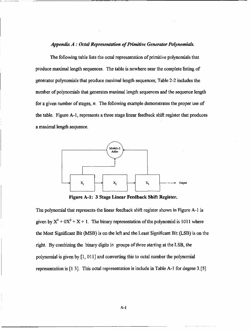
Appendix A : Octal Representation of Primitive Generator Polynomials.
The following table lists the octal representation of primitive polynomials that
produce maximal length sequences. The table is nowhere near the complete listing of
generator polynomials that produce maximal length sequences; Table 2-2 includes the
number of polynomials that generates maximal length sequences and the sequence length
for a given number of stages, n. The following example demonstrates the proper use of
the table. Figure A-i, represents a three stage linear feedback shift register that produces
a maximal length sequence.
x ----- X2 3 -- ---- -b- Output
Figure A-i: 3 Stage Linear Feedback Shift Register.
The polynomial that represents the linear feedback shift register shown in Figure A-1 is
given by X3 + OX 2 + X + 1. The binary representation of the polynomial is 1011 where
the Most Significant Bit (MSB) is on the left and the Least Significant Bit (LSB) is on the
right. By combining the binary digits in groups of three starting at the LSB, the
polynomial is given by [1, 011] and converting this to octal number the polynomial
representation is [1 3]. This octal representation is include in Table A-1 for degree 3.[5]
A-1

Table A-i: Octal Representation of Primitive Generator Polynomials.
De2ree Octal Representation ( do on right to d. on left)
2 [7]
3 [13], [15]
4 [23], [37]
5 [45], [75], [67]
6 [103], [147], [155]
7 [211], [217], [235], [367], [277], [325], [203],[313], [345]
8 [435], [551], [747], [453], [545], [537], [703],[543]
9 [1021], [1131], [1461], [1423], [1055], [1167],[1541], [1333], [1605], [1743], [1617], [1553]
10 [2011], [2415], [3771], [2157], [3515], [2773],[2033], [2443], [2461], [3023], [3543], [2745]
11 [4005], [4445], [4215], [4055], [6015], [7413],[4143], [4563], [4053], [5023], [5623], [4577]
12 [10123], [15647], [16533], [16047], [11015],[14127], [17673], [13565], [15341], [15053]
13 [20033], [23261], [24623], [23517], [30741],[21643], [30171], [21277], [27777], [35051]
14 [42103], [43333], [51761], [40503], [77141],[62677], [44103], [45145], [76303], [64457]
15 [100003], [102043], [110013], [102067], [104307],[100317], [177775], [103451], [110075], [102061]
16 [210013], [234313], [233303], [307107], [307527],[306357], [201735], [272201], [242413], [270155]
A-2

Degree Octal Representation ( do on right to d,_ on left)
17 [400011], [400017], [400431], [525251], [410117],[400731], [411335], [444257], [600013], [403555]
18 [1000201], [1000247], [1002241], [1002441],[1100045], [1000407], [1003011], [1020121]
19 [2000047], [2000641], [2001441], [2000107],[2000077], [2000157], [2000175], [2000257]
20 [4000011], [4001051], [4004515], [6000031],[4442235]
21 [10000005], [10040205], [10020045], [10040315],[10000635], [10103075], [10050335], [10002135]
22 [20000003], [20001043], [22222223], [25200127],[20401207], [20430607], [20070217]
23 [40000041], [40404041], [40000063], [40010061],[50000241], [40220151], [40006341], [40405463]
24 [100000207], [125245661], [113763063]
25 [200000011], [200000017], [204000051 ],[200010031], [200402017], [252001251]
26 [400000107], [430216473], [402365755],[426225667], [510664323], [473167545]
27 [1000000047], [1001007071], [1020024171],[1102210617], [1250025757], [1257242631]
28 [2000000011], [2104210431], [2000025051],[2020006031], [2002502115], [2001601071]
29 [4000000005], [4004004005], [4000010205],[4010000045], [4400000045], [4002200115]
30 [10040000007], [10104264207], [10115131333],[11362212703], [10343244533]
A-3
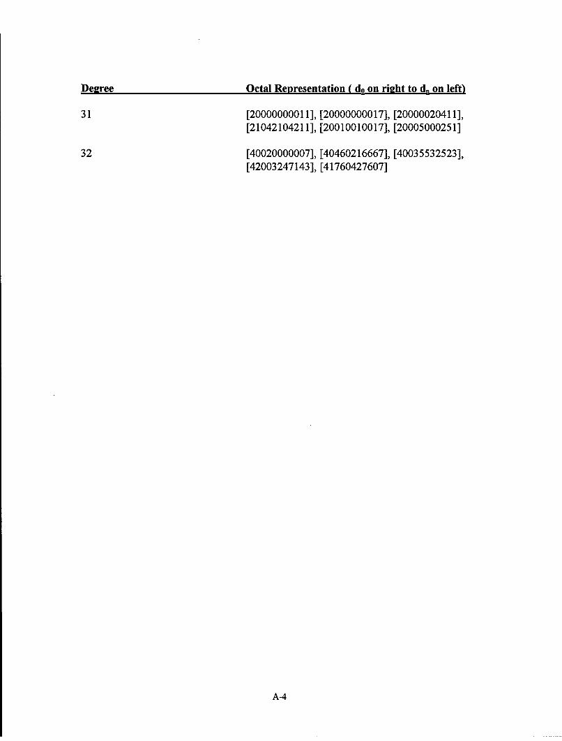
Degree Octal Representation ( do on ri2ht to d, on left)
31 [20000000011], [20000000017], [20000020411],[21042104211], [20010010017], [20005000251]
32 [40020000007], [40460216667], [40035532523],[42003247143], [41760427607]
A-4
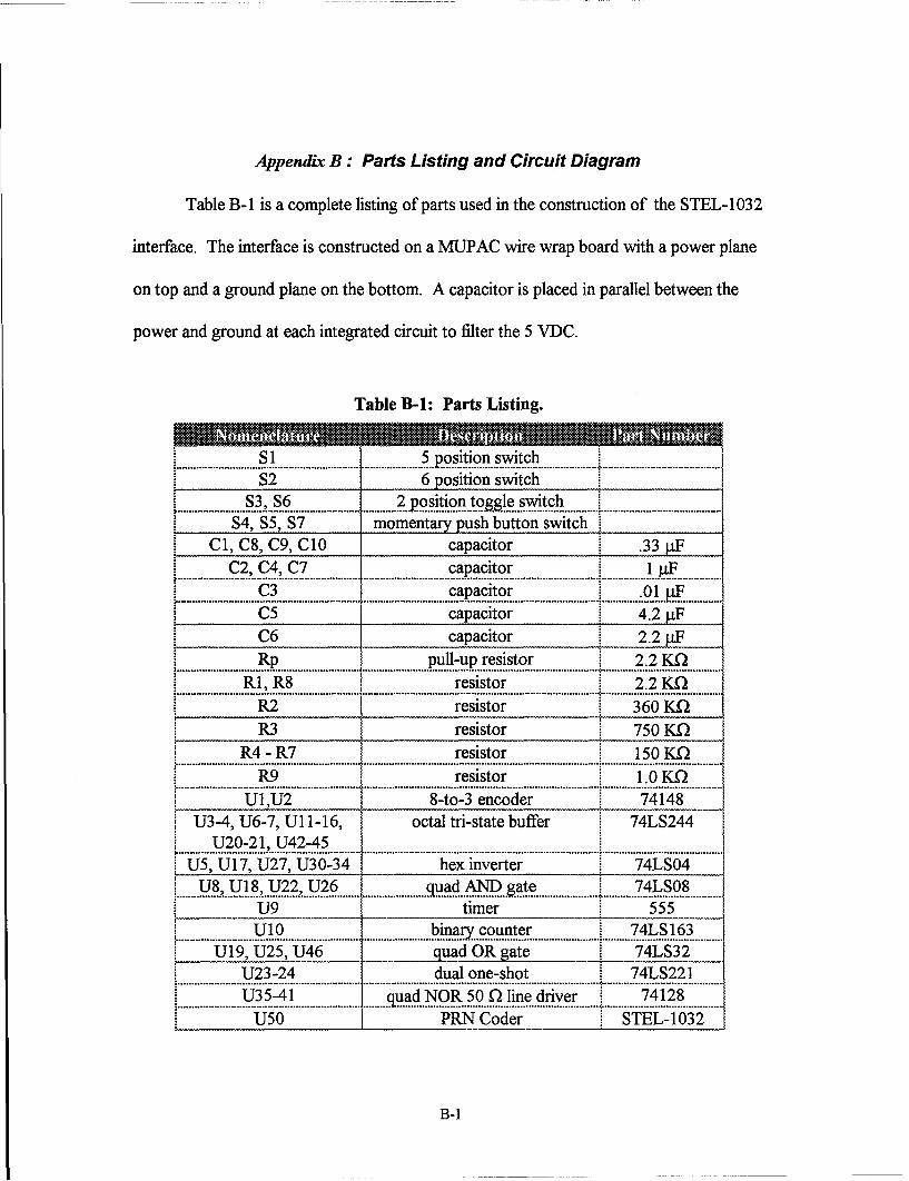
Appendix B: Parts Listing and Circuit Diagram
Table B-1 is a complete listing of parts used in the construction of the STEL-1032
interface. The interface is constructed on a MUPAC wire wrap board with a power plane
on top and a ground plane on the bottom. A capacitor is placed in parallel between the
power and ground at each integrated circuit to filter the 5 VDC.
Table B-i: Parts Listing.
. ........ ......... .. ..................................................................S2 6 position switch
S3,S6 2 position toggle switchS......................... ..s...3.......s.6........................... ................ .o. !..!..o.........t.o. ...•.e..s . c....... ....... . ..............................................$4, S5, $7 momentary push button switch
Cl, C8, C9, CIO capacitor .33 p.FC2, C4, C7 capacitor 1 PFS................ ..C.• ,....C..4 ,...C.7 ......................................................o.......................................... ...................
C3capacitor .01 p.F................................................................................... ... a •i o.............................................,o... .............C5 capacitor 4.2 IiFC6 capacitor 2.2 pFRp pull-up resistor 2.2 M~................................................ ..............................................................p u -u . s! ..o . ............ .......................... ...L • .............
RI, R8 resistor 2.2 KI)R2 resistor 360 KIQR3 resistor 750 KM)
R4 - R7 resistor 150 K.Q................................................................. ........................................ ........................................... ............................................
R9 resistor 1.0 KK2U1,U2 8-to-3 encoder 74148
U3-4, U6-7, U1 1-16, octal tri-state buffer 74LS244U20-21, U42-45S......... o 0 - .b .. 4 • -4.5. ....... ............ ........................................................................... ....... ..
U5, U17, U27, U30-34 hex inverter 74LS04U8, U18, U22, U26 quad AND gate 74LS08.................. . , ...• ....... • . •.............. .......... ........ . ........... ..... W .. .......................... ........... ...4 . s...0....8.. ............ ..
U9 timer 555..... binary counter 74LS163............................................... ..............................................................•n .• u .t...r ......... ............................7.4.S.1.6 ...........
U19, U25, U46 quad OR gate 74LS32U23-24 dual one-shot 74LS221.................................................................. .....................................................................................
.....................
U35-41 .....quadN R 50.Q line driver 74128...........................................3. ...-.4 .1 .........................................o• .•....n....l~ .• . .... ......................7 .a..2..s...............U50 PRN Coder STEL-1032
B-i
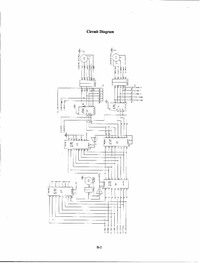
Circuit Diagram
0 0 A
0 f�) 0
�
COder 2
Code Coot
for Oavoeer NOUNS 5,2 Cd E.g - o
CO
� � 0

Circuit Diagram (cont.)
-,o
.,2C
i-zz •"•oI•L
t -
C
UZ
a, C
C)B--

Circuit Diagram (cont.)
Tj JfTfltf s;e
-4 4 - - U421
-4 -4 -4 -442414
,~ ~~~ 24 , - 0 - - 2
S~ 2~
B-4

Circuit Diagram (cont.)U46-3
4b 5b4 U42 150
6b7b8b9b1 Gb1 1 b 17 Vcc=2o
GND=I 0
U46-6
119
12b 2 18-- U12-18
13b 4 U43 16 - u12-16S14 -1 U12-1415b 8 12-- U12-1216b 11 9- U12-917b 13 7----- - - U2-7
18b 15 5 U12-517 Vcc=20 3
19b GND=IO U12-3
U46-8
2 1820b 4 U 44 1621b
2b6 14220
23b 8 1211 9
24b 13_725b 15_526b27b 17 Vcc=20 3
GND=l 0
U46-1 1
290
28b 2 U45 18
29b 4 6
30b30c
29c2c13 7
28c2c15 5
27c17 Vcc=20 326c GND=l 0
B-5

Circuit Diagram (cont.)
U5-4
1 F 1 9
Ul14-18 2 enab I e 18U 14-16 - _4 16
U14-14• 6 U20 14
U14-12- -8 12
U14-9, 11 9
U 4-7 13 Vcc=20 7
U14-5, 15 GND=I 0 5
U1 4-3, 17 3Buffer D0
"",- U50-53-- -- - --- -- U50-54
U5-3 Q D U
U) enoble 18 D U50-57
U21 14 D 6 U50-59L 12 D U50-60
J 9E Vcc=20 700o GND=I 0 5L0 3
Buffer
B-6

Circuit Diagram (cont.)
1= C= 0 0C
fI-hh
(Dt
00
o rn
C
(0
0.
C:r
C (-D
Cn
(AN) ~N)
Coo
LD Cn
(N) -00 01 0~~C
0 C
N) N)r0 N
U. 00
B-7r

Circuit Diagram (cont.)
U2-413 27 > 2 :ýj1 2c 3Ul 2-1
2 U46
44-
Ul 78 5U25b6 B-3-

Circuit Diagram (cont.)
U)
< >)
U,:
01 0
C)<
-< N
10 - 0 ,
11 1 -U
0
cmn
< D CI
L)0 U1
-4 0
_71 -C ý
U,
0
ID
B-9
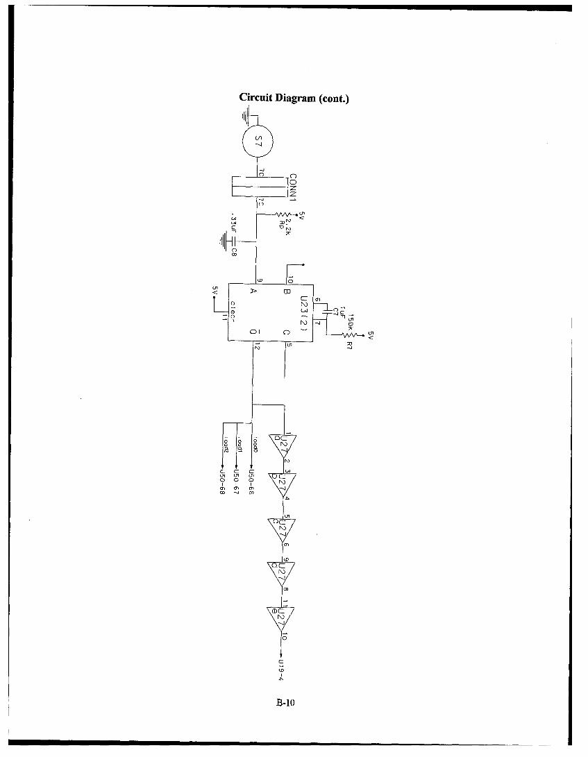
Circuit Diagram (cont.)
-TI
C)m0
Lnz
LMz
C)
0o 0
B--

Circuit Diagram (cont.)
5V
9C 17ýarU50-50
2 U22 ~ ]Ul 9b 6 lcOu50-5
5IC 122 19 10A Ul J E8 ok U50-1
Co 25 V 1-0 U2c8 13ý U1dllck U 5 0-6 5
BB-l

Circuit Diagram (cont.)
U5-7 XOR01 2 L30 2 C N
U50a20 XOR01 2U0
U5-1 MXCOD 5U3 6 N
U50-204 3UC 123 3
U50-21- CUE >U31 2 c1
U50-22. EP9HO 3 >01 Li- dLT
3-2
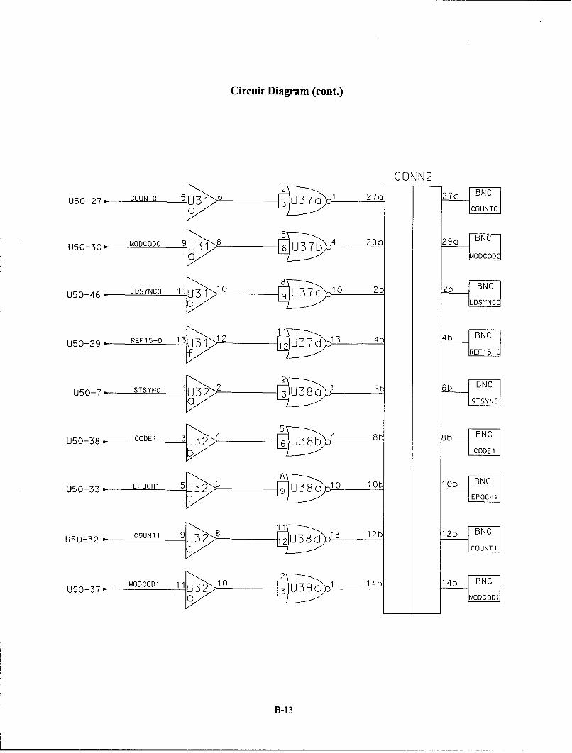
Circuit Diagram (cont.)
CONN2
U5-7 COUNTO 6 U3 17c 6c P
U50-27~ UOD >3E- 13 837ý3 LO
U50-45
U50-79c STYNNU3C
U50-30 EPOCODi 9U31 66 51 L- 9
U50>d COUNi 3 32
U50-46 MODYCOD 11U31 108 37 10 2Zb 6NC
-13
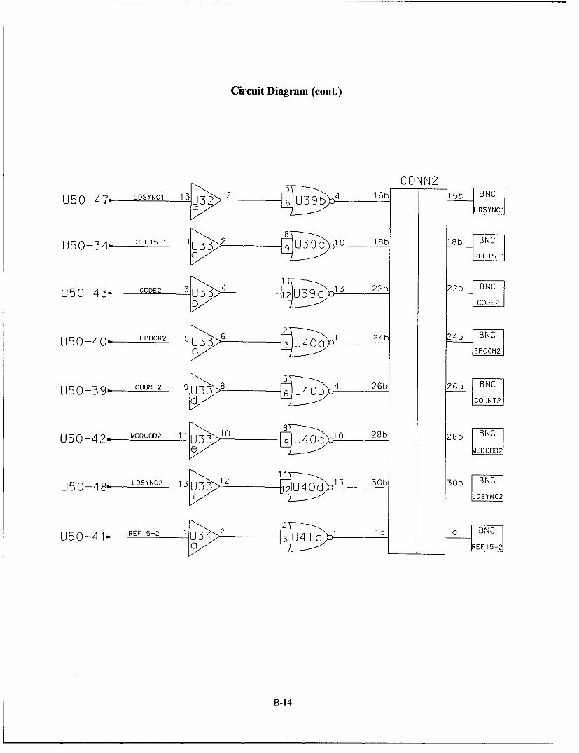
Circuit Diagram (cont.)
U5 -T LDSYNC1 1 3 '3 1 2 L7 41b16 IBN
U50-47 OE L3U33 .39b4-DYC
REF42 15-1OD 108b1b
U50-348 IDYC U 12 39C1
U504G REF5- 15-1
CODE2 4ý U13 22B2-14
Bibliography
1. Dixon, Robert C. Spread Spectrum Systems. New York : John Wiley & Sons, 1984.
2. Golomb, Solomon, W. Shift Register Sequences. Laguna Hills, California: AegeanPark Press, 1982.
3. Michelson, Arnold M. and Allen H. Levesque. Error-Control Techniques for DigitalCommunication. New York: John Wiley & Sons, 1985.
4. Peterson, Roger L., Rodger E. Ziemer and David E. Borth. Introduction to SpreadSpectrum Communications. New Jersey: Prentice Hall, 1995.
5. Peterson, William W. and E. J. Weldon Jr. Error-Correcting Codes. Massachusetts:The MIT Press, 1972.
6. Sklar, Bernard. Digital Communications: Fundamentals and Applications. NewJersey: Prentice Hall, 1988.
7. Soclof, Sidney. Design and Applications of Analog Integrated Circuits. New Jersey:Prentice Hall, 1991.
8. Spliker, James J. Global Positioning System: Theory and Applications. Washington,D.C.: American Institute of Aeronautics and Astronautics, 1988
9. Zavrel, Robert J. The Spread Spectrum Handbook. Santa Clara, California: StanfordTelecommunications, Inc., 1990
BIB-1

Vita
Captain John F. Brendle Jr. was born in Wayne, Michigan on October 2, 1966.
After graduating from St. Francis DeSales High School in Columbus, Ohio, he attended
The Ohio State University. He graduated with a Bachelor of Science in Electrical
Engineering and was commissioned a 2nd Lieutenant in the United States Air Force on
March 16, 1990. His first assignment was Undergraduate Pilot Training (UPT) in
December of 1990. In November 1991, he was assigned to the Aerospace Guidance and
Metrology Center at Newark Air Force Base. In December of 1995, he was selected to
attend the Air Force Institute of Technology and pursue a Master of Science in Electrical
Engineering starting in July 1996. His follow on assignment will be with the National
Reconnaissance Office in Chantilly, Virginia.
Permanent Address: 2034 Balmoral CourtColumbus, Ohio 43229
VITA-1

REPORT DOCUMENTATION PAGE Form ApprovedOMB No. 0704-0188
Public reporting burden for this collection of information is estimated to average 1 hour per response, including the time for reviewing instructions, searching existing data sources,gathering and maintaining the data needed, and completing and reviewing the collection of information. Send comments regarding this burden estimate or any other aspect of thiscollection of information, including suggestions for reducing this burden, to Washington Headquarters Services, Directorate for Information Operations and Reports, 1215 JeffersonDavis Highway, Suite 1204, Arlington, VA 22202-4302, and to the Office of Management and Budget, Paperwork Reduction Project (0704-0188), Washington, DC 20503.
1. AGENCY USE ONLY (Leave blank) 2. REPORT DATE 3. REPORT TYPE AND DATES COVERED
December 1997 Master's Thesis4. TITLE AND SUBTITLE 5. FUNDING NUMBERS
Pseudorandom Code Generation for Communication and Navigation SystemApplications
6. AUTHOR(S)John F. Brendle Jr., Captain, USAF
7. PERFORMING ORGANIZATION NAME(S) AND ADDRESS(ES) S. PERFORMING ORGANIZATION
Air Force Institue of Technology REPORT NUMBER
AFIT/GE/ENG/97D-16
9. SPONSORING/MONITORING AGENCY NAME(S) AND ADDRESS(ES) 10. SPONSORING/MONITORINGWright Laboratory AGENCY REPORT NUMBER
Avionics DirectorateWright-Patterson AFB, OH 45433-7333
11. SUPPLEMENTARY NOTES
12a. DISTRIBUTION AVAILABILITY STATEMENT 12b. DISTRIBUTION CODE
Approved for public release; distribution unlimited
13. ABSTRACT (Maximum 200 words)
This research project investigated the design, construction and evaluation of a pseudorandom code generator forcommunication and navigation system applications. These types of codes include spreading codes, Gold codes, JetPropulsion Laboratory (JPL) ranging codes, syncopated codes, and non-linear codes. Such waveforms are typically used incommunication and navigation system applications. The code generator uses the Stanford Telecom STEL-1032Pseudorandom Number (PRN) coder. A coder interface was designed and constructed for manual data entry to the registersof the PRN coder. The code generator is capable of independently clocking and generating all possible codes with lengths upto 4,294,967,295 bits. The codes can be started with any random phase. The code generator is capable of detecting aspecific position in the code and the coders can be truncated and restarted at that point. The three independent coder outputsare combinable, expanding the lengths and versatility of the codes. The generation of a non-linear code is possible using aninternally programmable look-up table. Several test were conducted on the code generator to ensure its capability ofgenerating Gold codes, JPL ranging codes, syncopated codes, and non-linear codes. The required documentation is beingsubmitted for a U.S. patent.
14. SUBJECT TERMS 15. NUMBER OF PAGESPseudorandom Code, Spread Spectrum, Code Generator 100
16. PRICE CODE
17. SECURITY CLASSIFICATION 18. SECURITY CLASSIFICATION 19. SECURITY CLASSIFICATION 20. LIMITATION OF ABSTRACTOF REPORT OF THIS PAGE OF ABSTRACT
UNCLASSIFIED UNCLASSIFIED UNCLASSIFIED ULStandard Form 298 (Rev. 2-89) (EG)Prescribed by ANSI Std. 239.18Designed using Perform Pro, WHS/DIOR, Oct 94