160322 resistive gate ccd kmpd9005e03 - · PDF file1 Resistive gate type CCD linear image...
37
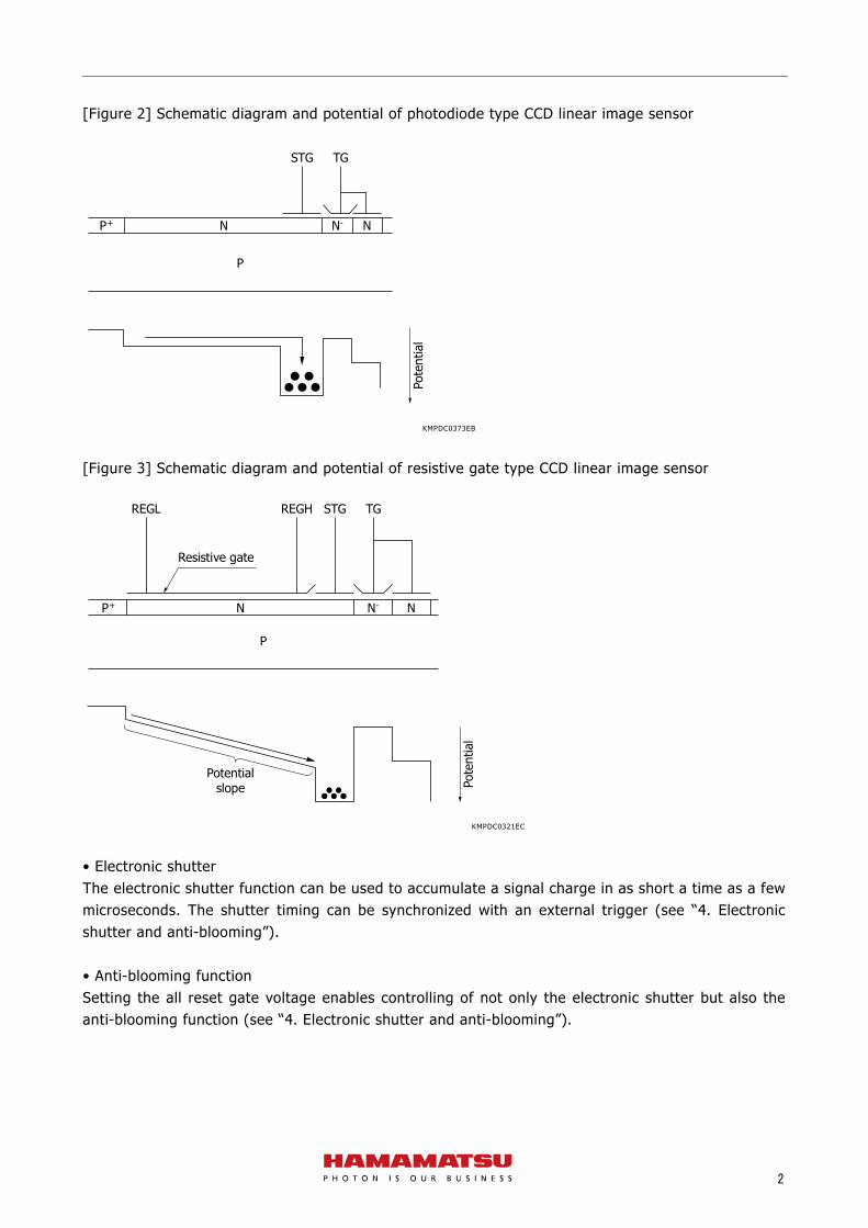
1 Resistive gate type CCD linear image sensor with electronic shutter function 1. Features Long photosensitive area, high-speed transfer of charges from the photosensitive area, small image lag In ordinary CCD image sensors, one pixel contains multiple electrodes and a signal charge is transferred by applying different clock pulses to those electrodes [Figure 1]. In photodiode type CCD linear image sensors, because there is no potential slope in the active area, very large image lag occurs for rectangular pixels [Figure 2]. In resistive gate structures, a single high-resistance electrode is formed in the active area, and a signal charge is transferred by means of a potential slope that is created by applying different voltages across the electrode [Figure 3]. Compared to a CCD area image sensor which is used as a linear sensor by line binning, a resistive gate type CCD linear image sensor offers higher speed transfer of charges in the photosensitive area. In addition, compared to photodiode types, resistive gate types can transfer charges with small image lag in a short period of time even for long photosensitive areas. [Figure 1] Schematic diagram and potential of ordinary 2-phase drive CCD area image sensor KMPDC0320EB P1V P2V P1V P2V N N P N N - N - N - N - N Potential T echnical information
Transcript of 160322 resistive gate ccd kmpd9005e03 - · PDF file1 Resistive gate type CCD linear image...

1
Resistive gate type CCD linear image sensor with electronic shutter function
1. Features
Long photosensitive area, high-speed transfer of charges from the photosensitive area, small image lag
In ordinary CCD image sensors, one pixel contains multiple electrodes and a signal charge is transferred by applying different clock pulses to those electrodes [Figure 1]. In photodiode type CCD linear image sensors, because there is no potential slope in the active area, very large image lag occurs for rectangular pixels [Figure 2]. In resistive gate structures, a single high-resistance electrode is formed in the active area, and a signal charge is transferred by means of a potential slope that is created by applying different voltages across the electrode [Figure 3]. Compared to a CCD area image sensor which is used as a linear sensor by line binning, a resistive gate type CCD linear image sensor offers higher speed transfer of charges in the photosensitive area. In addition, compared to photodiode types, resistive gate types can transfer charges with small image lag in a short period of time even for long photosensitive areas. [Figure 1] Schematic diagram and potential of ordinary 2-phase drive CCD area image sensor
KMPDC0320EB
P1V P2V P1V P2V
N N
P
N N-N-N-N- N
Pote
ntia
l
Technical information
2
[Figure 2] Schematic diagram and potential of photodiode type CCD linear image sensor
KMPDC0373EB
[Figure 3] Schematic diagram and potential of resistive gate type CCD linear image sensor
KMPDC0321EC
• Electronic shutter The electronic shutter function can be used to accumulate a signal charge in as short a time as a few microseconds. The shutter timing can be synchronized with an external trigger (see “4. Electronic shutter and anti-blooming”).
• Anti-blooming function Setting the all reset gate voltage enables controlling of not only the electronic shutter but also the anti-blooming function (see “4. Electronic shutter and anti-blooming”).
NN-P+ N
P
STG TG
Pote
ntia
l
NN-P+ N
P
REGL REGH STG TG
Potentialslope
Resistive gate
Pote
ntia
l
3
• Capable of both non-MPP operation and MPP operation When performing repeated measurements over a short integration time (e.g., 1 ms or less) in which dark current can be ignored, use the sensor in the state where a potential slope is always formed at all times (non-MPP operation). On the other hand, when accumulating over a long integration time, dark current may be a problem. In this situation, apply a specific voltage to the resistive gate during integration. This will set the portions under the resistive gate to the inverted state, thus reducing the dark current (MPP operation, see “5. Non-MPP operation and MPP operation”).
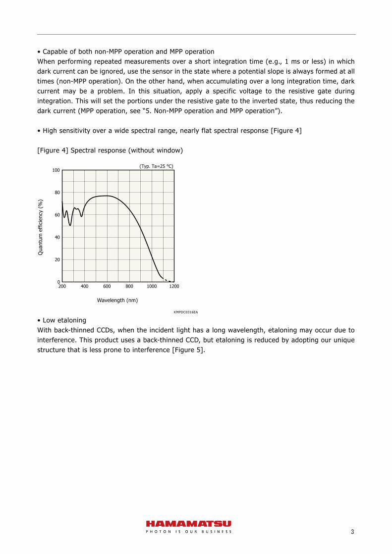
• High sensitivity over a wide spectral range, nearly flat spectral response [Figure 4] [Figure 4] Spectral response (without window)
KMPDC0316EA
• Low etaloning With back-thinned CCDs, when the incident light has a long wavelength, etaloning may occur due to interference. This product uses a back-thinned CCD, but etaloning is reduced by adopting our unique structure that is less prone to interference [Figure 5].
Wavelength (nm)
(Typ. Ta=25 °C)
Qua
ntum
effi
cien
cy (
%)
0
100
80
60
40
20
1200200 400 600 800 1000

4
[Figure 5] Etaloning characteristics (typical example)
KMPDC0284EB
Wavelength (nm)
Rela
tive
sens
itivi
ty (
%)
900 1000950 960 970 980 990930910 940920
(Ta=25 °C)
Etaloning-improved type
Previous type
0
40
30
20
10
50
60
70
80
90
100
110
5
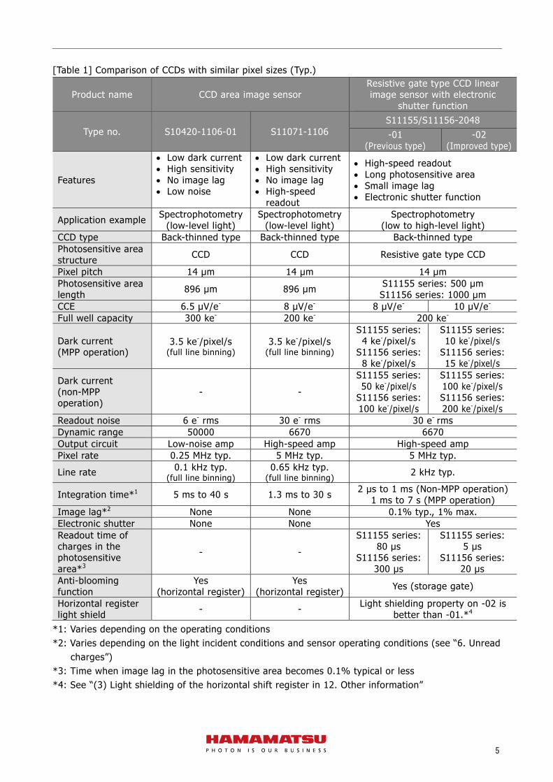
[Table 1] Comparison of CCDs with similar pixel sizes (Typ.)
Product name CCD area image sensor Resistive gate type CCD linear image sensor with electronic
shutter function
Type no. S10420-1106-01 S11071-1106 S11155/S11156-2048 -01
(Previous type) -02
(Improved type)
Features
Low dark current High sensitivity No image lag Low noise
Low dark current High sensitivity No image lag High-speed
readout
High-speed readout Long photosensitive area Small image lag Electronic shutter function
Application example Spectrophotometry(low-level light)
Spectrophotometry(low-level light)
Spectrophotometry (low to high-level light)
CCD type Back-thinned type Back-thinned type Back-thinned type Photosensitive area structure CCD CCD Resistive gate type CCD
Pixel pitch 14 µm 14 μm 14 μm Photosensitive area length 896 μm 896 μm S11155 series: 500 μm
S11156 series: 1000 μm CCE 6.5 μV/e- 8 μV/e- 8 μV/e- 10 μV/e- Full well capacity 300 ke- 200 ke- 200 ke-
Dark current (MPP operation)
3.5 ke-/pixel/s (full line binning)
3.5 ke-/pixel/s (full line binning)
S11155 series: 4 ke-/pixel/s
S11156 series: 8 ke-/pixel/s
S11155 series: 10 ke-/pixel/s
S11156 series: 15 ke-/pixel/s
Dark current (non-MPP operation)
- -
S11155 series: 50 ke-/pixel/s
S11156 series: 100 ke-/pixel/s
S11155 series: 100 ke-/pixel/s S11156 series: 200 ke-/pixel/s
Readout noise 6 e- rms 30 e- rms 30 e- rms Dynamic range 50000 6670 6670 Output circuit Low-noise amp High-speed amp High-speed amp Pixel rate 0.25 MHz typ. 5 MHz typ. 5 MHz typ.
Line rate 0.1 kHz typ. (full line binning)
0.65 kHz typ. (full line binning)
2 kHz typ.
Integration time*1 5 ms to 40 s 1.3 ms to 30 s 2 μs to 1 ms (Non-MPP operation) 1 ms to 7 s (MPP operation)
Image lag*2 None None 0.1% typ., 1% max. Electronic shutter None None Yes Readout time of charges in the photosensitive area*3
- -
S11155 series: 80 μs
S11156 series: 300 μs
S11155 series: 5 μs
S11156 series: 20 μs
Anti-blooming function
Yes (horizontal register)
Yes (horizontal register) Yes (storage gate)
Horizontal register light shield - - Light shielding property on -02 is
better than -01.*4 *1: Varies depending on the operating conditions *2: Varies depending on the light incident conditions and sensor operating conditions (see “6. Unread
charges”) *3: Time when image lag in the photosensitive area becomes 0.1% typical or less *4: See “(3) Light shielding of the horizontal shift register in 12. Other information”
6
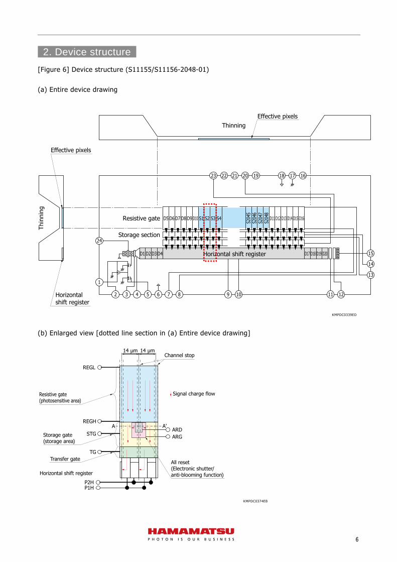
2. Device structure
[Figure 6] Device structure (S11155/S11156-2048-01) (a) Entire device drawing
KMPDC0339ED
(b) Enlarged view [dotted line section in (a) Entire device drawing]
KMPDC0374EB
Effective pixels
Effective pixels
Horizontalshift register
Thinning
15
14
13
2 3 4 5 6 7 8 9 10 11 12
Thin
ning
23 22 21 20 19 16
1
24
1718
Resistive gate
Storage section
Horizontal shift registerS2
045
S204
6S2
047
S204
8
D5 D6 D7 D8 D9 D10 S1 S2 S3 S4 D11 D12 D13 D14 D15 D16
D17 D18 D19 D20D1 D2 D3 D4
REGL
Resistive gate(photosensitive area)
Storage gate(storage area)
Channel stop
ARDARG
REGHA A'
STG
TG
P2HP1H
14 µm 14 µm
All reset(Electronic shutter/anti-blooming function)
Transfer gate
Horizontal shift register
Signal charge flow

7
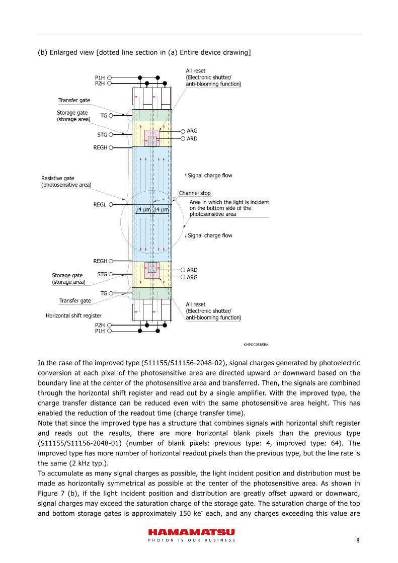
[Figure 7] Device structure (S11155/S11156-2048-02) (a) Entire device drawing
KMPDC0543EB
Horizontal CCD shift register D77 D78 D79 D80D63 D64
Horizontal CCD shift register D77 D78 D79 D80D63 D64
9 10 11 12
15
14
13
7
8
21
23
20
22 19 161718
Resistive gate area
Storage area
S204
5S2
046
S204
7S2
048
D65 D66 D67 D68 D69 D70 S1 S2 S3 S4 D71 D72 D73 D74 D75 D76
Thinning
Thin
ning
・・
・・
・・
・・2
1
24
3 45 6
D1D2
Effective pixels
Effectivepixels
Horizontalshift register
Horizontalshift register
・・
・・
8
(b) Enlarged view [dotted line section in (a) Entire device drawing]
KMPDC0585EA
In the case of the improved type (S11155/S11156-2048-02), signal charges generated by photoelectric conversion at each pixel of the photosensitive area are directed upward or downward based on the boundary line at the center of the photosensitive area and transferred. Then, the signals are combined through the horizontal shift register and read out by a single amplifier. With the improved type, the charge transfer distance can be reduced even with the same photosensitive area height. This has enabled the reduction of the readout time (charge transfer time). Note that since the improved type has a structure that combines signals with horizontal shift register and reads out the results, there are more horizontal blank pixels than the previous type (S11155/S11156-2048-01) (number of blank pixels: previous type: 4, improved type: 64). The improved type has more number of horizontal readout pixels than the previous type, but the line rate is the same (2 kHz typ.). To accumulate as many signal charges as possible, the light incident position and distribution must be made as horizontally symmetrical as possible at the center of the photosensitive area. As shown in Figure 7 (b), if the light incident position and distribution are greatly offset upward or downward, signal charges may exceed the saturation charge of the storage gate. The saturation charge of the top and bottom storage gates is approximately 150 ke- each, and any charges exceeding this value are
Channel stop
All reset(Electronic shutter/anti-blooming function)
Storage gate(storage area)
Storage gate(storage area)
REGH
STG
TGTransfer gate
Transfer gate
ARDARG
Signal charge flow
Signal charge flow
P2HP1H
Horizontal shift register
REGL
All reset(Electronic shutter/anti-blooming function)
Resistive gate(photosensitive area)
REGH
STG
TG
ARDARG
P1HP2H
14 µm 14 µmArea in which the light is incidenton the bottom side of thephotosensitive area
9
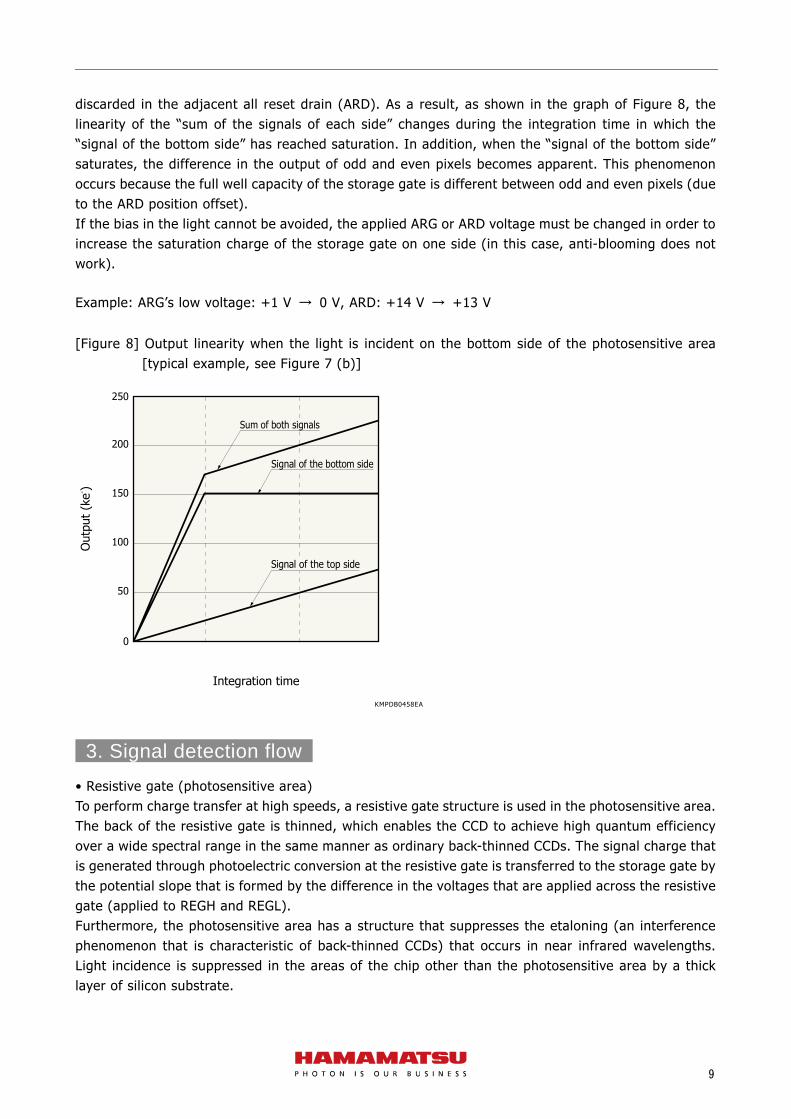
discarded in the adjacent all reset drain (ARD). As a result, as shown in the graph of Figure 8, the linearity of the “sum of the signals of each side” changes during the integration time in which the “signal of the bottom side” has reached saturation. In addition, when the “signal of the bottom side” saturates, the difference in the output of odd and even pixels becomes apparent. This phenomenon occurs because the full well capacity of the storage gate is different between odd and even pixels (due to the ARD position offset). If the bias in the light cannot be avoided, the applied ARG or ARD voltage must be changed in order to increase the saturation charge of the storage gate on one side (in this case, anti-blooming does not work). Example: ARG’s low voltage: +1 V → 0 V, ARD: +14 V → +13 V
[Figure 8] Output linearity when the light is incident on the bottom side of the photosensitive area
[typical example, see Figure 7 (b)]
KMPDB0458EA
3. Signal detection flow
• Resistive gate (photosensitive area) To perform charge transfer at high speeds, a resistive gate structure is used in the photosensitive area. The back of the resistive gate is thinned, which enables the CCD to achieve high quantum efficiency over a wide spectral range in the same manner as ordinary back-thinned CCDs. The signal charge that is generated through photoelectric conversion at the resistive gate is transferred to the storage gate by the potential slope that is formed by the difference in the voltages that are applied across the resistive gate (applied to REGH and REGL). Furthermore, the photosensitive area has a structure that suppresses the etaloning (an interference phenomenon that is characteristic of back-thinned CCDs) that occurs in near infrared wavelengths. Light incidence is suppressed in the areas of the chip other than the photosensitive area by a thick layer of silicon substrate.
Integration time
Out
put
(ke- )
0
50
250
150
200
100
Sum of both signals
Signal of the bottom side
Signal of the top side

10
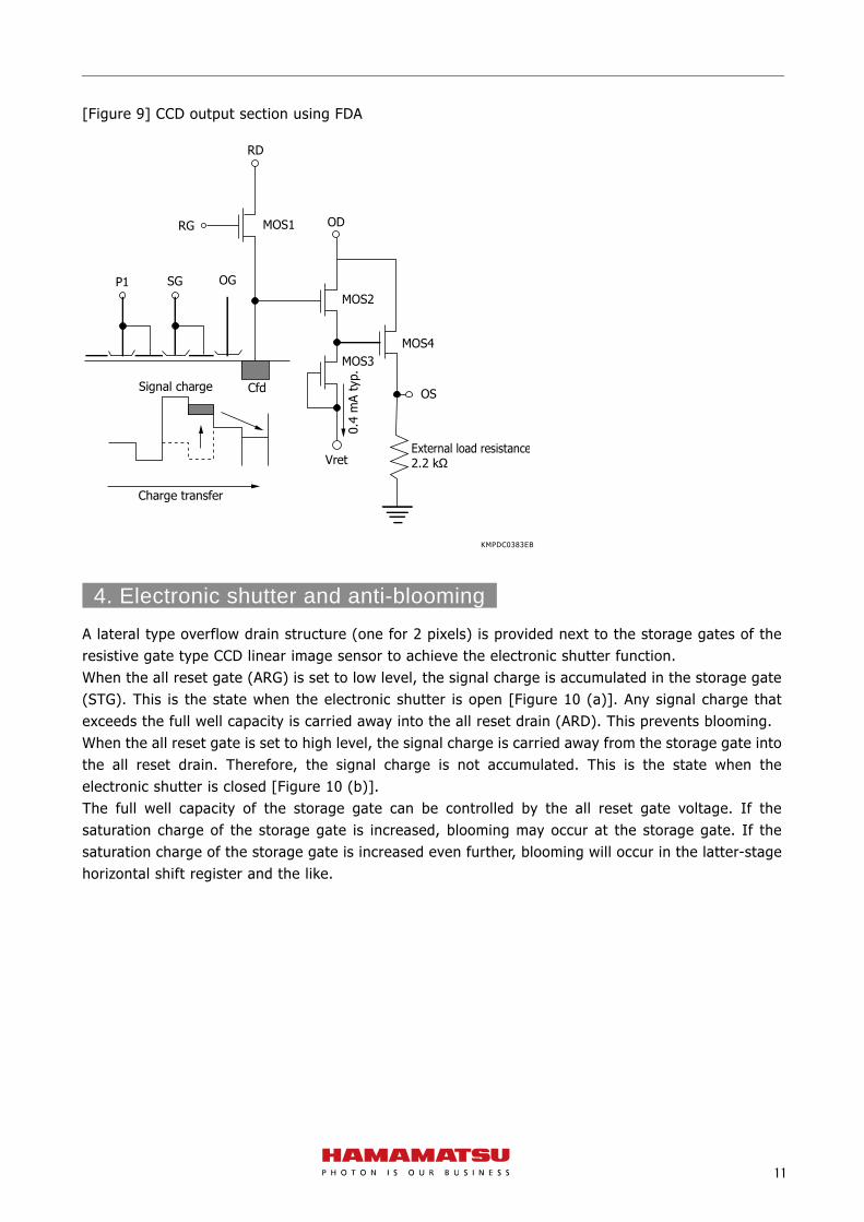
• Storage gate The signal charge that is transferred from the resistive gate is accumulated in the storage gate. A lateral type anti-blooming structure is next to the storage gate. This provides both an anti-blooming function and an electronic shutter function (see “4. Electronic shutter and anti-blooming”). • Transfer gate The transfer gate is located between the storage gate and the horizontal shift register. When the transfer gate is set to high level, the signal charge that is accumulated in the storage gate is transferred to the transfer gate. When the transfer gate is then set to low level, the signal charge is transferred to the horizontal shift register. • Horizontal shift register The signal charge that has been transferred to the horizontal shift register is transferred to the output stage when clock pulses are applied to the horizontal shift register. • Output stage A MOSFET for charge-to-voltage conversion that is known as an FDA (floating diffusion amplifier) is embedded in the output stage [Figure 9]. The signal charge is transferred to capacitance Cfd, and the charge-to-voltage conversion occurs [Equation (1)].
Vfd = Signal charge / Cfd ・・・・・・・・・・・・ (1)
Vfd: output voltage This voltage is impedance-converted through a two-stage MOSFET source follower circuit (gain < 1) and output from the OS terminal. Because the CCD does not include an external load resistance (2.2 kΩ), it must be provided through an external circuit.
11
[Figure 9] CCD output section using FDA
KMPDC0383EB
4. Electronic shutter and anti-blooming
A lateral type overflow drain structure (one for 2 pixels) is provided next to the storage gates of the resistive gate type CCD linear image sensor to achieve the electronic shutter function. When the all reset gate (ARG) is set to low level, the signal charge is accumulated in the storage gate (STG). This is the state when the electronic shutter is open [Figure 10 (a)]. Any signal charge that exceeds the full well capacity is carried away into the all reset drain (ARD). This prevents blooming. When the all reset gate is set to high level, the signal charge is carried away from the storage gate into the all reset drain. Therefore, the signal charge is not accumulated. This is the state when the electronic shutter is closed [Figure 10 (b)]. The full well capacity of the storage gate can be controlled by the all reset gate voltage. If the saturation charge of the storage gate is increased, blooming may occur at the storage gate. If the saturation charge of the storage gate is increased even further, blooming will occur in the latter-stage horizontal shift register and the like.
RG
RD
MOS1 OD
Vret
MOS2
MOS3MOS4
OS
0.4
mA
typ.
P1 SG OG
Signal charge
Charge transfer
External load resistance2.2 kΩ
Cfd
12
[Figure 10] Schematic diagram and potential of all reset section (cross-section structure of the area denoted by broken line A-A' in [Figure 6 (b)])
(a) ARG: low level, Electronic shutter: open [integration state (anti-blooming state)]
KMPDC0375EA
(b) ARG: high level, Electronic shutter: closed (reset state)
KMPDC0376EA
Integration time When an electronic shutter is used, the integration time is defined as the time from when the all reset gate is set to low level to when the accumulated signal charge is transferred to the horizontal shift register (the length of time until the transfer gate becomes low level [Figure 11]). Any signal charge that is generated outside of this period is carried away into the all reset drain during the period that the all reset gate is set to high level and is not read out as signals. If the electronic shutter function is not used, the all reset gate is set to low level at all times. In this situation, the integration time is the same as the readout cycle.
N- N+N-
P+ P+NN
Potential
STGARGARD
Potential
N- N-
P+ P+NN
STGARGARD
N+
13
[Figure 11] Timing chart (when electronic shutter is in use)
KMPDC0287EC
5. Non-MPP operation and MPP operation
MPP (multi-pinned phase) operation is performed by setting the portions under all MOS structure gates, which constitute the CCD electrodes, to the inverted state (except for storage gate). In MPP operation, the oxide film interface is inverted by holes supplied from the channel stop region. The generation of thermally excited electrons on the oxide film interface is drastically suppressed, thus resulting in a state with low dark current. This state is known as pinning. By precisely applying the pinning voltage (the gate voltage during pinning), the dark current can be greatly reduced. This operation is suitable for integrations over a long period of time. Consider the amount of dark current generated and the length of time needed to read out the signals (shutter time), and select non-MPP operation or MPP operation according to the operating conditions. (1) Non-MPP operation In non-MPP operation, a different fixed voltage is applied to the resistive gate (REGH, REGL) to form a potential slope at all times. In this situation, if a voltage lower than the pinning voltage is applied, the potential slope does not form in the CCD channels, and the image lag increases. In non-MPP operation, because the portions under the resistive gate are not in the pinning state, the dark current becomes large. However, this operation is suitable for integrations over a short period of time where the effect of dark current is small. Non-MPP operation is suitable when detecting intense light by using an electronic shutter to decrease the integration time and reduce the incident light level. The potentials at various times [Figure 12] in non-MPP operation are shown in Figure 13. T1 The signal charge that is generated through photoelectric conversion at the resistive gate (REG) is transferred to the storage gate by the potential slope. T2 The all reset gate is set to high level. The signal charge is carried away into the all reset drain. Any signal charge that was generated by incident light before this period is not read out (electronic shutter: closed). T3 The all reset gate is set to low level, and signal charge is integrated (electronic shutter: open).
All reset gate
Transfer gate
Horizontal shift register*
Readout period
Integration time
Readout cycle
14
T4 The transfer gate is set to high level. The signal charge that was accumulated in the storage gate is transferred to the transfer gate. Note that a portion of the signal charge that is generated during this period is also read out. T5 P1H is set to high level. Note that a portion of the signal charge that is generated during this period is also read out. T6 The transfer gate is set to low level. The signal charge is transferred from the transfer gate to the horizontal shift register (P1H). After this point, when clock pulses are applied to P1H and P2H, the signal charge is transferred to the output stage via the horizontal shift register.
[Figure 12] Timing chart (S11156-2048-02, non-MPP operation)
KMPDC0377EC
Output period of one line
Tinteg(electronic shutter: open)
Tpwv
Tpwr
ARG
REGH, REGL
TG
P1H 1 2
P2H
SG
RG
OS
3..2127 2130... N*1
*1: Set the total number N of clock pulses according to the integration time.Apply clock pulses to appropriate terminals during dummy readout period.
*2: To prevent noise from being superimposed on the OS at the falling edge of the ARG clock pulse,set the ARG rise/fall time to 200 ns or more.
2129
Dummy readout period
T1 T2 T4 T5 T6T3
D1 D2 D79 D80
Normal readout period
Tpwh, Tpws
(REGH=+1 V, REGL=-7 V)
Tovr
D3..D70, S1...S2048, D77, D78
2128
*2
Tpwar(electronic shutter: closed)
15
[Figure 13] Potentials at various times in non-MPP operation
KMPDC0379EB
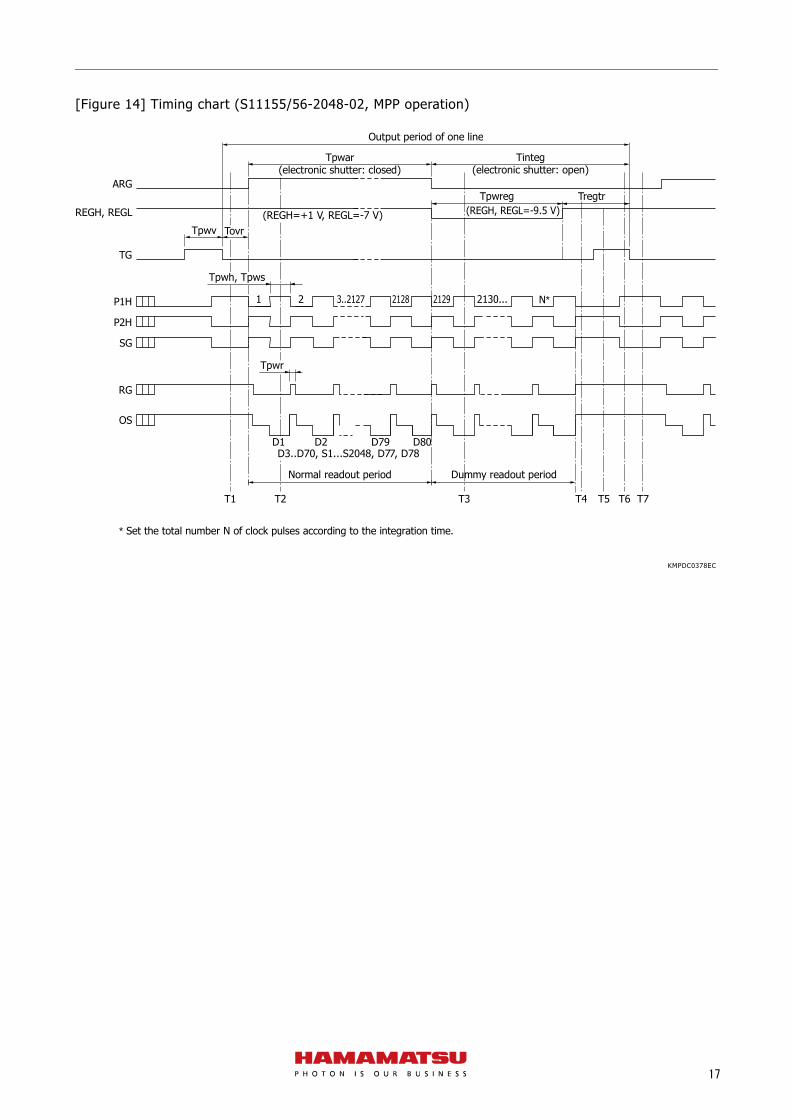
(2) MPP operation In MPP operation, the same pinning voltages are applied to both ends of the resistive gate to reduce dark current during integration. MPP operation is suitable for detecting low-level light over a long time period. However, because the image lag in the photosensitive area becomes large in this state, when transferring the charge, to form a potential slope, a voltage must be applied to the resistive gate at the same level as the voltage applied during non-MPP operation, and the readout time must be set to ① or ② shown below. To apply anti-blooming at intense level, ① is recommended.
① Change the REGH and REGL voltage levels to high before the TG level becomes high to make the
high level time longer [Figure 14].
NNN
REGL REGH STG TG P1H P2H
P
N-N-N-P+ N
T1
T2
T3
T4
T5
T6
Reset

16
② Make the high level voltage period of REGH and REGL longer by synchronizing to the TG high level period (Tpwv).
The potentials at various times [Figure 14] in MPP operation are shown in Figure 15.
T1 The signal charge that is generated by light entering the resistive gate (REG) is accumulated in the storage gate. T2 The all reset gate is set to high level. The signal charge is carried away into the all reset drain. Any signal charge that was generated by incident light before this period is not read out (electronic shutter: closed).
T3 The all reset gate is set to low level, and signal charge is integrated (electronic shutter: open). The voltage that is applied across the resistive gate is set to a voltage that is less than the pinning voltage. This is the state in which the dark current generated in the resistive gate is reduced (the potential slope does not form). T4 Different voltages are applied across the resistive gate. The potential slope forms, and the signal charge that was generated by light entering the resistive gate is transferred to the storage gate. Note that a portion of the signal charge that is generated during this period is also read out. T5 The transfer gate is set to high level. The signal charge that was accumulated in the storage gate is transferred to the transfer gate. Note that a portion of the signal charge that is generated during this period is also read out. T6 P1H is set to high level. Note that a portion of the signal charge that is generated during this period is also read out. T7 The transfer gate is set to low level. The signal charge is transferred from the transfer gate to the horizontal shift register (P1H). After this point, when clock pulses are applied to P1H and P2H, the signal charge is transferred to the output stage via the horizontal shift register.
17
[Figure 14] Timing chart (S11155/56-2048-02, MPP operation)
KMPDC0378EC
Output period of one line
Tinteg(electronic shutter: open)
Tpwv
T1
ARG
REGH, REGL
TG
P1H 1
D2 D79 D80
2
P2H
SG
RG
OS
3..2127 2130...2128 2129
(REGH, REGL=-9.5 V)
Normal readout period
T2 T3 T5T4 T6 T7
(REGH=+1 V, REGL=-7 V)
Tpwreg Tregtr
Tpwh, Tpws
Tovr
Tpwr
D3..D70, S1...S2048, D77, D78D1
Dummy readout period
Tpwar(electronic shutter: closed)
N*
* Set the total number N of clock pulses according to the integration time.

18
[Figure 15] Potentials at various times in MPP operation
KMPDC0380EB
6. Unread charges
Unread charges (image lag) are defined as a percentage of the signal level left unread of the incident light level and are expressed by equation (2).
T7
T6
T5
NNNP
N-N-N-P+ N
T1
T2
Reset
REGL REGH STG TG P1H P2H
T3
T4
19
L = (Slag/S) × 100 [%] ・・・・・・・・・(2)
L: image lag Slag: unread signal level S: input signal level
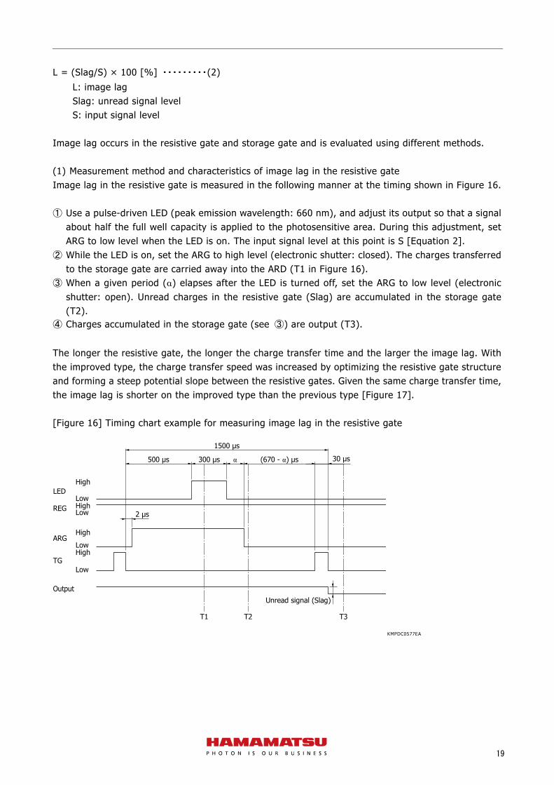
Image lag occurs in the resistive gate and storage gate and is evaluated using different methods. (1) Measurement method and characteristics of image lag in the resistive gate Image lag in the resistive gate is measured in the following manner at the timing shown in Figure 16.
① Use a pulse-driven LED (peak emission wavelength: 660 nm), and adjust its output so that a signal
about half the full well capacity is applied to the photosensitive area. During this adjustment, set ARG to low level when the LED is on. The input signal level at this point is S [Equation 2].
② While the LED is on, set the ARG to high level (electronic shutter: closed). The charges transferred to the storage gate are carried away into the ARD (T1 in Figure 16).
③ When a given period (α) elapses after the LED is turned off, set the ARG to low level (electronic shutter: open). Unread charges in the resistive gate (Slag) are accumulated in the storage gate (T2).
④ Charges accumulated in the storage gate (see ③) are output (T3).
The longer the resistive gate, the longer the charge transfer time and the larger the image lag. With the improved type, the charge transfer speed was increased by optimizing the resistive gate structure and forming a steep potential slope between the resistive gates. Given the same charge transfer time, the image lag is shorter on the improved type than the previous type [Figure 17]. [Figure 16] Timing chart example for measuring image lag in the resistive gate
KMPDC0577EA
Unread signal (Slag)
HighLED
REG
T1 T2 T3
ARG
Output
TG
LowHighLow
High
HighLow
Low
500 µs
2 µs
300 µs α (670 - α) µs 30 µs
1500 µs

20
[Figure 17] Image lag in the resistive gate vs. time (α) (typical example)
KMPDB0450EA
Relationship between the image lag in the resistive gate and input light pulse width Figure 19 shows the image lag when the input signal level is constant and the LED’s light emission pulse width is changed at the timing shown in Figure 18. The larger the pulse width, the smaller the image lag. As the signal charge that is converted from the incident light is transferred to the storage gate by the potential slope of the resistive gate, the image lag will be smaller when a low level light is applied over a long time period. [Figure 18] Timing chart example for measuring image lag in the resistive gate
KMPDC0578EA
0.001
0.01
0.1
1
10
100
0 10 20 30 40 50 60
Imag
e la
g (%
)
α (µs)
(Ta=25 °C)
S11156-2048-02
S11155-2048-02
S11156-2048-01
S11155-2048-01
LED
TG
30 µs
ARG
500 µs
* 2 µs, 5 µs, 10 µs, 100 µs, 300 µs
Light emissionpulse width* α µs
2 µs
1500 µs

21
[Figure 19] Image lag in the resistive gate vs. incident light pulse width (typical example) (a) S11155-2048-01/-02 (α=5 μs)
KMPDB0451EA
(b) S11156-2048-01/-02 (α=20 μs)
KMPDB0452EA
(2) Measurement method and characteristics of image lag in the storage gate As shown in Figure 20, a pulse-driven LED (peak emission wavelength: 660 nm) is used at about half the saturation output. After sufficient time (approx. 500 s) elapses for the charge generated in the resistive gate to be transferred to the storage, the TG voltage is set to high level to transfer the charge to the horizontal shift register. Most of the input signal level (S) of equation (2) is read out during the first output period, and the remaining signal (Slag) is output during the second output period. It is possible to reduce the image lag in the storage gate as the TG high level period (Tpwv) is
(Average of all pixels)
Imag
ela
g(%
)
Incident light pulse width (µs)
20.01
100
10
1
0.1
5 10 100 300
S11155-2048-01S11155-2048-02
(Average of all pixels)
Imag
ela
g(%
)
Incident light pulse width (µs)
20.01
100
10
1
0.1
5 10 100 300
S11156-2048-01S11156-2048-02

22
increased. With the improved type, the potential structure of the storage gate is optimized to reduce the image lag in the storage gate as compared to the previous type [Figure 21].
[Figure 20] Timing chart example for measuring image lag in the storage gate (Non-MPP operation)
KMPDC0579EA
[Figure 21] Image lag in the storage gate vs. TG_high period (typical example)
KMPDB0453EA
7. Dark current temperature dependence
Dark current has temperature dependence. For example, in the case of the S11156-2048-02, the temperature dependence during MPP operation is as shown in Figure 22.
Input signal level (S)
Second output period
Unread signal level (Slag)
High
300 µs 500 µs
LED
REG
ARG
Output
TG
Low
HighLow
High
HighLow
Low
Tpwv
First output period
0.001
0.01
0.1
1
0.1 1
TG_high period (µs)
Imag
e la
g (%
)
10010
(Ta=25 °C)
S11156-2048-01
S11156-2048-02
23
[Figure 22] Dark current temperature dependence (S11156-2048-02, MPP operation, typical example)
KMPDB0454EA
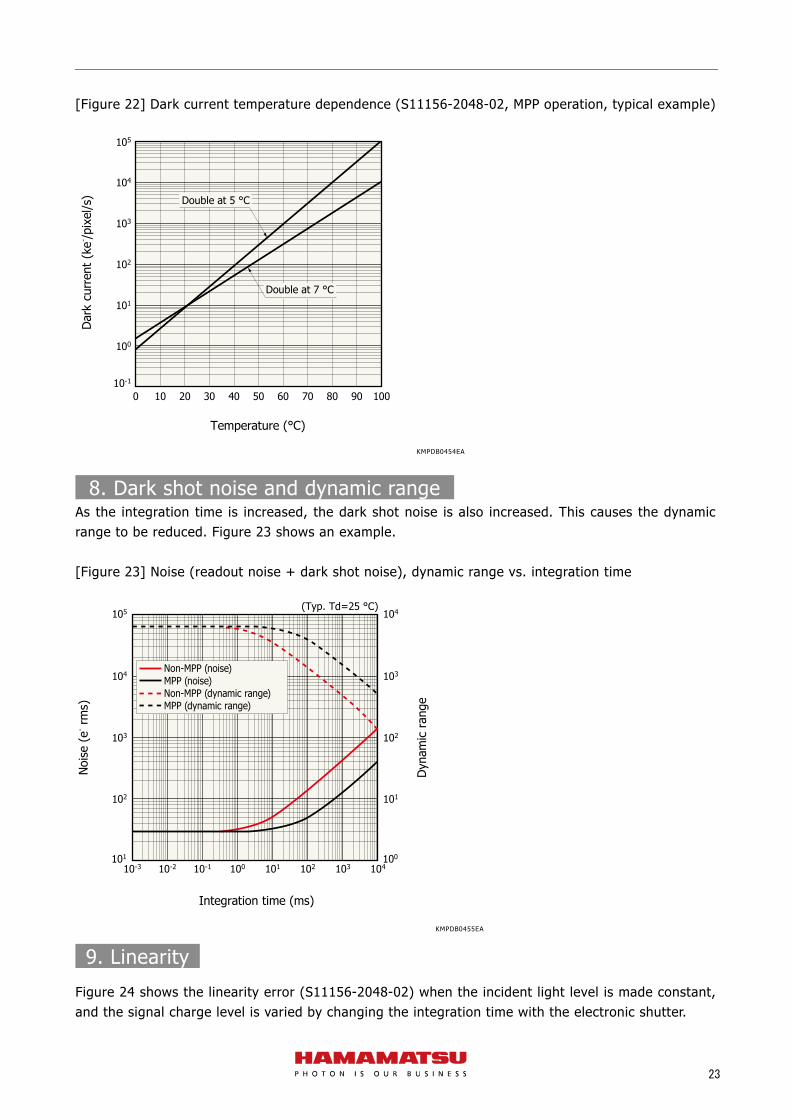
8. Dark shot noise and dynamic range As the integration time is increased, the dark shot noise is also increased. This causes the dynamic range to be reduced. Figure 23 shows an example. [Figure 23] Noise (readout noise + dark shot noise), dynamic range vs. integration time
KMPDB0455EA
9. Linearity
Figure 24 shows the linearity error (S11156-2048-02) when the incident light level is made constant, and the signal charge level is varied by changing the integration time with the electronic shutter.
Temperature (°C)
Dar
k cu
rren
t (k
e- /pix
el/s
)
0 10 20 30 40 50 60 70 80 90 100
105
104
102
103
101
100
10-1
Double at 5 °C
Double at 7 °C
101
102
103
104
105
100
101
102
103
104
10-3 10-2 10-1
Integration time (ms)
Noi
se (
e- rm
s)
Dyn
amic
ran
ge
104103101100 102
(Typ. Td=25 °C)
Non-MPP (noise)MPP (noise)Non-MPP (dynamic range)MPP (dynamic range)
24
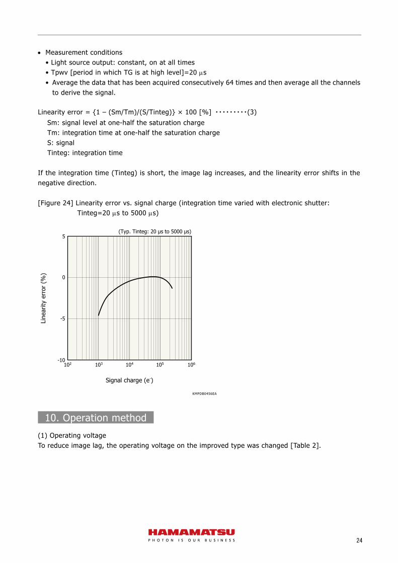
Measurement conditions • Light source output: constant, on at all times • Tpwv [period in which TG is at high level]=20 s • Average the data that has been acquired consecutively 64 times and then average all the channels
to derive the signal. Linearity error = 1 – (Sm/Tm)/(S/Tinteg) × 100 [%] ・・・・・・・・・(3)
Sm: signal level at one-half the saturation charge Tm: integration time at one-half the saturation charge S: signal Tinteg: integration time
If the integration time (Tinteg) is short, the image lag increases, and the linearity error shifts in the negative direction. [Figure 24] Linearity error vs. signal charge (integration time varied with electronic shutter:
Tinteg=20 s to 5000 s)
KMPDB0456EA
10. Operation method
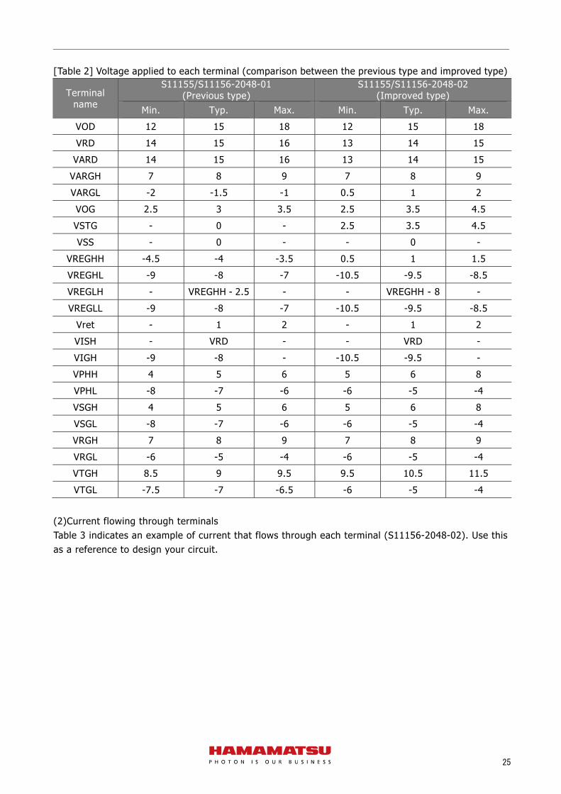
(1) Operating voltage To reduce image lag, the operating voltage on the improved type was changed [Table 2].
Signal charge (e-)
(Typ. Tinteg: 20 µs to 5000 µs)
Line
arity
err
or (
%)
103 104102-10
5
-5
0
105 106
25
[Table 2] Voltage applied to each terminal (comparison between the previous type and improved type)
Terminal name
S11155/S11156-2048-01(Previous type)
S11155/S11156-2048-02 (Improved type)
Min. Typ. Max. Min. Typ. Max.
VOD 12 15 18 12 15 18
VRD 14 15 16 13 14 15
VARD 14 15 16 13 14 15
VARGH 7 8 9 7 8 9
VARGL -2 -1.5 -1 0.5 1 2
VOG 2.5 3 3.5 2.5 3.5 4.5
VSTG - 0 - 2.5 3.5 4.5
VSS - 0 - - 0 -
VREGHH -4.5 -4 -3.5 0.5 1 1.5
VREGHL -9 -8 -7 -10.5 -9.5 -8.5
VREGLH - VREGHH - 2.5 - - VREGHH - 8 -
VREGLL -9 -8 -7 -10.5 -9.5 -8.5
Vret - 1 2 - 1 2
VISH - VRD - - VRD -
VIGH -9 -8 - -10.5 -9.5 -
VPHH 4 5 6 5 6 8
VPHL -8 -7 -6 -6 -5 -4
VSGH 4 5 6 5 6 8
VSGL -8 -7 -6 -6 -5 -4
VRGH 7 8 9 7 8 9
VRGL -6 -5 -4 -6 -5 -4
VTGH 8.5 9 9.5 9.5 10.5 11.5
VTGL -7.5 -7 -6.5 -6 -5 -4
(2)Current flowing through terminals Table 3 indicates an example of current that flows through each terminal (S11156-2048-02). Use this as a reference to design your circuit.

26
[Table 3] Approximate current that flows through each terminal
Terminal name
S11155/ S11156-2048-01 S11155/S11156-2048-02
Supply voltage Current
(mA)
Supply voltage Current
(mA) Typ. Typ.
OS - - - -
OD +15 +6 +15 +6
OG +3 +0.1 +3.5 +0.1
SG +5/-7 +0.1/-0.1 +6/-5 +0.1/-0.1
Vret +1 -0.4 +1 -0.4
RD +15 <<0.1 +14 <<0.1
REGL -6.5/-8 -1/-0.2 -7/-9.5 -10/-0.2
REGH -4/-8 +1/-0.2 +1/-9.5 +10/-0.2
P2H +5/-7 +0.1/-0.1 +6/-5 +0.1/-0.1
P1H +5/-7 +0.1/-0.1 +6/-5 +0.1/-0.1
IG2H -8 -0.1 -9.5 -0.1
IG1H -8 -0.1 -9.5 -0.1
ARG +8/-1.5 +0.1/-0.1 +8/+1 +0.1/+0.1
ARD +15 <+0.1 +14 <+0.1
ISH +15(=VRD) <<+0.1 +14(=VRD) <<+0.1
STG +3 +0.1 +3.5 +0.1
NC(STG) - - - -
TG +9/-7 +0.1/-0.1 +10.5/-5 +0.1/-0.1
RG +8/-5 +0.1/-0.1 +8/-5 +0.1/-0.1
The Vret and REGL power supplies must be of a sink type, and REGH of a source type. The power supplies of other terminals must be of a source type if the applied voltage is positive and sink type if negative. Inrush current and the like are different from the values in Table 3 (they depend on the capacitance and resistance of the sensor and the driver circuit).
11. Use examples (1) Controlling the incident light level with electronic shutter If the incident light level is large, any signal charge that exceeds the saturation charge is carried away into the all reset drain. At this point, the signal output saturates and becomes constant, making the verification of the output difference between each pixel impossible. In such situations, the output difference between each pixel can be verified by controlling the signal level by varying the integration time with an electronic shutter [Figure 26]. Multiple signals with different integration times are acquired, and the data is processed using the signals of unsaturated pixels and their integration times to virtually increase the dynamic range. Note that the integration time can be reduced to 2 s in the case of a resistive gate type CCD linear image sensor with an electronic shutter function.
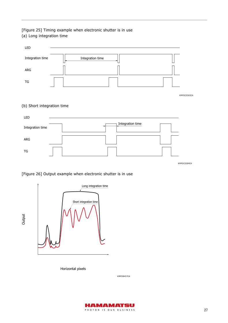
27
[Figure 25] Timing example when electronic shutter is in use (a) Long integration time
KMPDC0583EA
(b) Short integration time
KMPDC0584EA
[Figure 26] Output example when electronic shutter is in use
KMPDB457EA
Integration time
LED
Integration time
ARG
TG
Integration time
LED
Integration time
ARG
TG
Out
put
Horizontal pixels
Long integration time
Short integration time

28
(2) Integrating the signal obtained through multiple electronic shutter operations If the product is operated at the timing shown in Figure 27, excitation operation is repeated due to the
spark light, and the resulting fluorescence signal charge is accumulated temporarily in the transfer
gate. Then, the horizontal shift register can be used to read out the signal of each channel. This
readout method is effective in increasing the signal level when the signal light obtained by each
excitation operation is small.
[Figure 27] Timing chart (when accumulating and reading out the signal obtained through multiple electronic shutter operations)
KMPDC0581EA
12. Other information
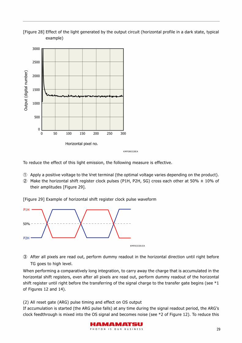
(1) Measures to eliminate the effect of light from the output circuit If the operating conditions are not appropriate, light may be generated from the output circuit. If this generated light is received by the resistive gate, storage gate, or horizontal shift registers, a phenomenon may occur in which the output is large for the first pixels that are read [Figure 28].
Spark light
Fluorescence
ARG
REG
TG
P1H
P2H
SG
RG
OS
Normal readout period
Electronic shutter: closed Electronic shutter: open
Dummy readout period
Output period of one line
Tpwar Tinteg
Tpwh Tpws
1
D1D3..D10. S1...S2048. D11..D18
D2 D19 D20
2 3.. 2068 2069 2070 N2067
Tinteg2Tinteg1
29
[Figure 28] Effect of the light generated by the output circuit (horizontal profile in a dark state, typical example)
KMPDB0328EA
To reduce the effect of this light emission, the following measure is effective. ① Apply a positive voltage to the Vret terminal (the optimal voltage varies depending on the product). ② Make the horizontal shift register clock pulses (P1H, P2H, SG) cross each other at 50% ± 10% of
their amplitudes [Figure 29]. [Figure 29] Example of horizontal shift register clock pulse waveform
KMPDC0381EA
③ After all pixels are read out, perform dummy readout in the horizontal direction until right before
TG goes to high level.
When performing a comparatively long integration, to carry away the charge that is accumulated in the horizontal shift registers, even after all pixels are read out, perform dummy readout of the horizontal shift register until right before the transferring of the signal charge to the transfer gate begins (see *1 of Figures 12 and 14).
(2) All reset gate (ARG) pulse timing and effect on OS output If accumulation is started (the ARG pulse falls) at any time during the signal readout period, the ARG’s clock feedthrough is mixed into the OS signal and becomes noise (see *2 of Figure 12). To reduce this
00
3000
2500
2000
1500
1000
500
50 100 150 200 250 300
Horizontal pixel no.
Out
put
(dig
ital n
umbe
r)
P1H
P2H
50%
30
effect, in the datasheet (S11155/S11156-2048-01/-02), the minimum value of the ARG’s fall time (Tpfar) is set to 200 ns. (3) Light-shielding of horizontal shift register When the back-thinned CCD is viewed from the light input side, the horizontal shift register is covered by the thick area of the silicon (insensitive area), and short-wavelength light hardly reaches the horizontal shift register. However, long-wavelength light may pass through the insensitive area of the silicon and may be received by the horizontal shift register [Figure 31]. If a mechanical shutter or the like is not used, light will enter the horizontal shift register during charge integration and transfer, and the spurious signal will be superimposed on the actual signal. For example, if a time invariant light enters the horizontal shift register, the output signal of each channel will increase by the same proportion. These effects will be smaller with shorter horizontal transfer time periods (higher output signal frequency).
The horizontal shift register is shielded from light in the following ways. ① Apply light only during the integration period, read out the unneeded charges accumulated in the
horizontal shift register during this period, and then read out the actual signal. ② Adjust the position where the light is directed to prevent light from entering the horizontal shift
register. ③ Attach a light-shielding mask to prevent light from entering the horizontal shift register. With the improved type, the horizontal shift register has been moved away from the photosensitive
area to reduce the effects of the light transmitted by light path 1. [Figure 31]. In addition, the
light-shielding metal attached to the front side of the CCD chip reduces components of light
transmitted through the photosensitive area, reflected by the metal film of the package (light path 2),
and entering the horizontal shift register. As a result, the light input to the horizontal shift register was
reduced to approximately 1/40 to 1/50 (LED peak wavelength: 880 nm) as compared with the previous
product.
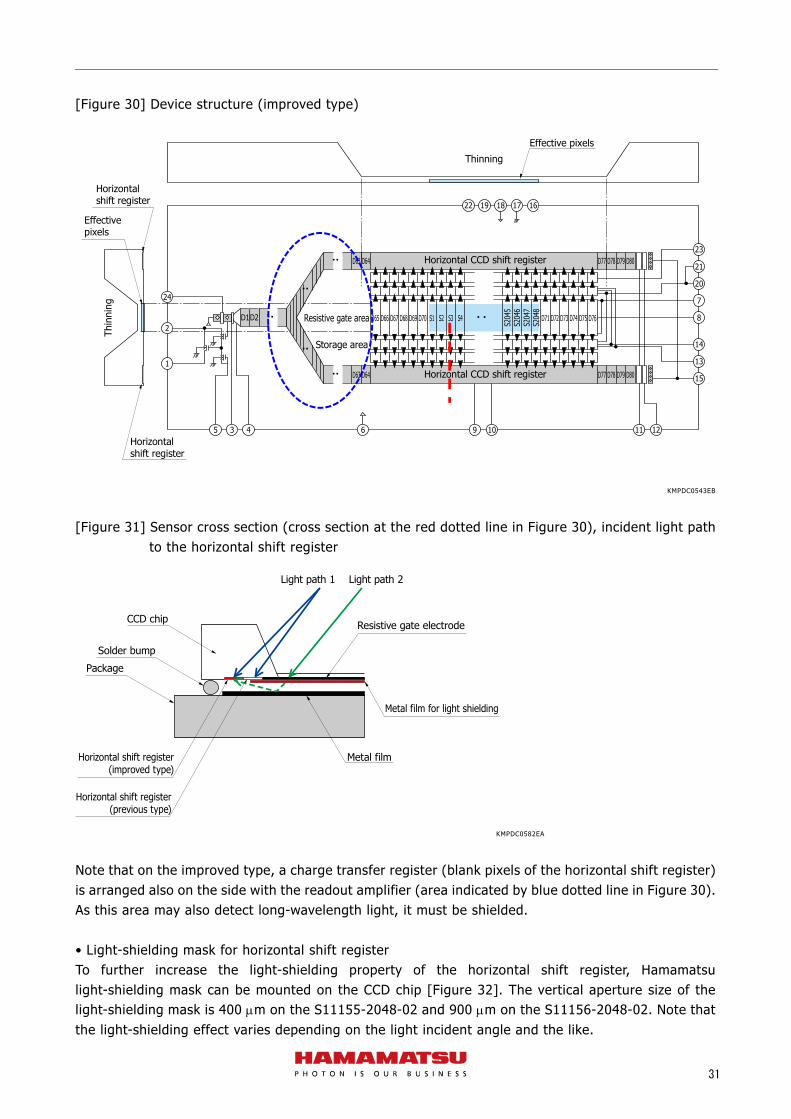
31
[Figure 30] Device structure (improved type)
KMPDC0543EB
[Figure 31] Sensor cross section (cross section at the red dotted line in Figure 30), incident light path
to the horizontal shift register
KMPDC0582EA
Note that on the improved type, a charge transfer register (blank pixels of the horizontal shift register) is arranged also on the side with the readout amplifier (area indicated by blue dotted line in Figure 30). As this area may also detect long-wavelength light, it must be shielded. • Light-shielding mask for horizontal shift register To further increase the light-shielding property of the horizontal shift register, Hamamatsu light-shielding mask can be mounted on the CCD chip [Figure 32]. The vertical aperture size of the light-shielding mask is 400 m on the S11155-2048-02 and 900 m on the S11156-2048-02. Note that the light-shielding effect varies depending on the light incident angle and the like.
Horizontal CCD shift register D77 D78 D79 D80D63 D64
Horizontal CCD shift register D77 D78 D79 D80D63 D64
9 10 11 12
15
14
13
7
8
21
23
20
22 19 161718
Resistive gate area
Storage area
S204
5S2
046
S204
7S2
048
D65 D66 D67 D68 D69 D70 S1 S2 S3 S4 D71 D72 D73 D74 D75 D76
Thinning
Thin
ning
・・
・・
・・
・・2
1
24
3 45 6
D1D2
Effective pixels
Effectivepixels
Horizontalshift register
Horizontalshift register
・・
・・
CCD chip
Solder bump
Package
Horizontal shift register(improved type)
Horizontal shift register(previous type)
Metal film
Metal film for light shielding
Resistive gate electrode
Light path 1 Light path 2

32
[Figure 32] Sensor configuration (light-shielding mask mounting: only available for the -02 type)
KMPDC0580EA
(4) Power consumption of resistive gate The resistive gate is composed of a high-resistance electrode. Applying a voltage across the resistive gate transfers the signal charge. In this situation, the resistive gate consumes the power that depends on the supply voltage and its electrode resistance [Table 4]. [Table 4] Power consumption and resistance of the resistive gate
Parameter Type no. Symbol Min. Typ. Max. Unit
Power consumption
S11155-2048-01
PREG
1.4 2.5 12.5
mW S11155-2048-02 50 100 160 S11156-2048-01 0.7 1.3 6.3 S11156-2048-02 30 60 90
Resistance
S11155-2048-01
RREG
0.5 2.5 4.5
kΩ S11155-2048-02 0.4 0.7 1.4 S11156-2048-01 1 5 9 S11156-2048-02 0.7 1.1 2.2
(5) Output waveform example The readout amplifier on the improved type is improved to support wide bandwidth.
S11155: 400 µmS11156: 900 µm
50 µ
m50
µm
CCD chip650 µm max.
120 µm
MaskHorizontal shift register
Effective area
Storage gate
Storage gate
Resistive gate(photosensitive area)
Horizontal shift register
Metal light-shielding film
Anti-reflection filmMask aperture area

33
[Figure 33] OS output waveform example (operating conditions: Typ., unless otherwise noted)
(a) S11155-2048-01 (fc=5 MHz typ.) (b) S11155-2048-02 (fc=10 MHz max.)
(6) Sensor temperature Figure 34 is a measurement example showing the relation between the sensor temperature and the operating time when the S11156-2048-01 is operated with our evaluation circuit (circuitry is placed a sealed case with no heat dissipation measures). The sensor temperature increases markedly when operated at high speed. Since the rise in the sensor temperature increases the dark current and accelerates device degradation, we recommend taking heat dissipation measures, such as attaching a heatsink to the sensor or using a cooling fan. If you want to achieve stable sensor temperature that is lower than room temperature, using a similar product, S13255/6 series, with a one-stage TE-cooler is recommended.
[Figure 34] Sensor temperature vs. operating time (using a Hamamatsu evaluation circuit)
KMPDB0331EA
DC level(reset level)
Sign
alRe
set f
eedt
hrou
gh
Signal level
020
50
45
40
35
30
25
20 40 60 80 100 120
Operation time (min)
Sens
or t
empe
ratu
re (
°C)
fc=5 MHz
fc=10 MHz
(Typ. Ta=25 °C)
34
13. Driver circuit
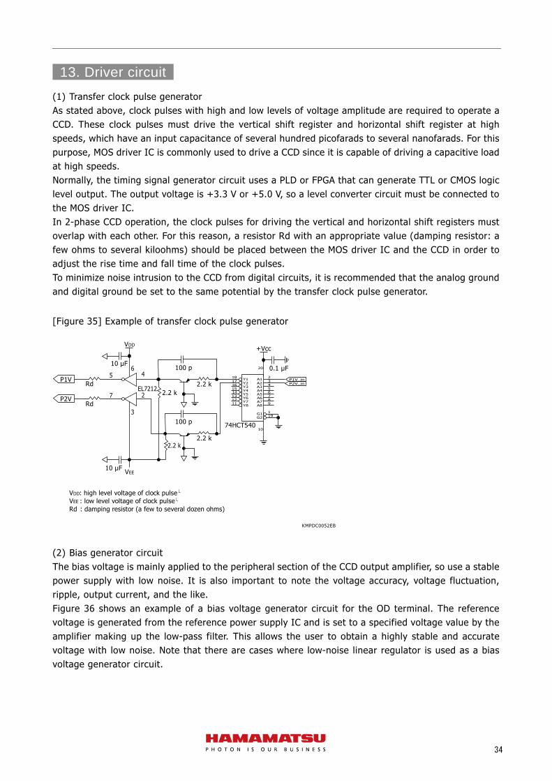
(1) Transfer clock pulse generator As stated above, clock pulses with high and low levels of voltage amplitude are required to operate a CCD. These clock pulses must drive the vertical shift register and horizontal shift register at high speeds, which have an input capacitance of several hundred picofarads to several nanofarads. For this purpose, MOS driver IC is commonly used to drive a CCD since it is capable of driving a capacitive load at high speeds. Normally, the timing signal generator circuit uses a PLD or FPGA that can generate TTL or CMOS logic level output. The output voltage is +3.3 V or +5.0 V, so a level converter circuit must be connected to the MOS driver IC. In 2-phase CCD operation, the clock pulses for driving the vertical and horizontal shift registers must overlap with each other. For this reason, a resistor Rd with an appropriate value (damping resistor: a few ohms to several kiloohms) should be placed between the MOS driver IC and the CCD in order to adjust the rise time and fall time of the clock pulses. To minimize noise intrusion to the CCD from digital circuits, it is recommended that the analog ground and digital ground be set to the same potential by the transfer clock pulse generator.
[Figure 35] Example of transfer clock pulse generator
KMPDC0052EB
(2) Bias generator circuit The bias voltage is mainly applied to the peripheral section of the CCD output amplifier, so use a stable power supply with low noise. It is also important to note the voltage accuracy, voltage fluctuation, ripple, output current, and the like. Figure 36 shows an example of a bias voltage generator circuit for the OD terminal. The reference voltage is generated from the reference power supply IC and is set to a specified voltage value by the amplifier making up the low-pass filter. This allows the user to obtain a highly stable and accurate voltage with low noise. Note that there are cases where low-noise linear regulator is used as a bias voltage generator circuit.
P1V_inP2V_in
P1V
VDD: high level voltage of clock pulseVEE : low level voltage of clock pulseRd : damping resistor (a few to several dozen ohms)
P2VRd
Rd
7
56
3
4
2EL7212
100 p
100 p
VDD+Vcc
VEE
74HCT540
2.2 k
2.2 k
2.2 k1817161514131211
23456789
119
10
20
Y1Y2Y3Y4Y5Y6Y7Y8
A1A2A3A4A5A6A7A8
G1G2
2.2 k
10 µF0.1 µF
10 µF
35
[Figure 36] Example of bias voltage generator circuit
KMPDC0303EA
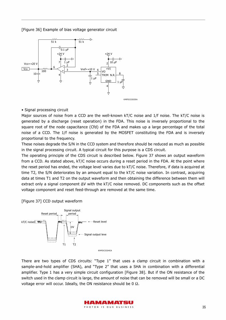
• Signal processing circuit Major sources of noise from a CCD are the well-known kT/C noise and 1/f noise. The kT/C noise is generated by a discharge (reset operation) in the FDA. This noise is inversely proportional to the square root of the node capacitance (Cfd) of the FDA and makes up a large percentage of the total noise of a CCD. The 1/f noise is generated by the MOSFET constituting the FDA and is inversely proportional to the frequency. These noises degrade the S/N in the CCD system and therefore should be reduced as much as possible in the signal processing circuit. A typical circuit for this purpose is a CDS circuit. The operating principle of the CDS circuit is described below. Figure 37 shows an output waveform from a CCD. As stated above, kT/C noise occurs during a reset period in the FDA. At the point where the reset period has ended, the voltage level varies due to kT/C noise. Therefore, if data is acquired at time T2, the S/N deteriorates by an amount equal to the kT/C noise variation. In contrast, acquiring data at times T1 and T2 on the output waveform and then obtaining the difference between them will extract only a signal component ∆V with the kT/C noise removed. DC components such as the offset voltage component and reset feed-through are removed at the same time. [Figure 37] CCD output waveform
KMPDC0304EA
There are two types of CDS circuits: “Type 1” that uses a clamp circuit in combination with a sample-and-hold amplifier (SHA), and “Type 2” that uses a SHA in combination with a differential amplifier. Type 1 has a very simple circuit configuration [Figure 38]. But if the ON resistance of the switch used in the clamp circuit is large, the amount of noise that can be removed will be small or a DC voltage error will occur. Ideally, the ON resistance should be 0 Ω.
VOD Vref=+10 V
+24 V
0.1 μF
10 μF1 μF
1 μF
VOD=+20 V
51 k 51 k
1006
7
4
+-
2
3 6
4
2
VOTRIM N.R.
GND
+VI
5 810
1 μF
+24 V
kT/C noise
T1
DV
T2
Reset periodSignal output
period
Signal output level
Reset level

36
[Figure 38] CDS circuit block diagram (using clamp circuit and SHA)
KMPDC0305EA
Type 2 uses a larger number of components but removes noise more effectively than Type 1. However, since Type 2 makes an analog calculation of the SHA output, the noise of the SHA itself may be added, resulting in increased noise in some cases. The SHA noise should be small enough so that the kT/C noise can be ignored.
[Figure 39] CDS circuit block diagram (using SHA and differential amplifier)
KMPDC0306EA
A circuit example of Type 1 is shown in Figure 40. The preamp gain should be set high in order to sufficiently amplify the CCD output signal. Since the CCD output signal contains DC voltage components, a capacitor is used for AC coupling. Note that this capacitor can cause a DC voltage error if the preamp bias current is large. Therefore, a preamp with a small bias current must be selected. A JFET or CMOS input amplifier is generally used. It is also necessary to select a low-noise amplifier with a bandwidth wide enough to amplify the CCD output waveform. The clamp circuit is made up of capacitors and an analog switch. As the analog switch, we recommend using a high-speed type having low ON resistance and small charge injection amount. As with the preamp, the last-stage amplifier is AC-coupled via a capacitor, so a JFET or CMOS input amplifier should be selected. In addition, a non-inverted amplifier must be configured to allow high input impedance. Incidentally the CCD provides a negative-going output while the last-stage amplifier gives a positive-going output to facilitate analog-to-digital conversion. For this reason, an inverted amplifier is
Clamp signal (T1)
Clamp circuit
CCD output
Clamp signal (T1)
Sample signal (T2)0 V
Video output
Sample-and-hold amp (SHA)
Video output
Buffer ampPreamp (LPF)
CCD output
Sample signal (T2)
Video output
Preamp (LPF)
Differential amp
Sample-and-holdamp (SHA)
CCD output
Sample signal 1 (T1)
+-
Sample signal 2 (T2)
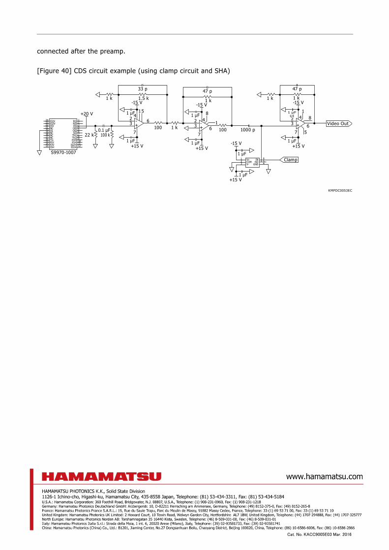
37
connected after the preamp. [Figure 40] CDS circuit example (using clamp circuit and SHA)
KMPDC0053EC
242322212019181716151413
123456789101112
IG1VIG2VISVNCSSNCNCNCTGP1VP2VISH
RGRDOSODOGSG
Th1Th2P2HP1H
IG2HIG1H
S9970-1007
+20 V
3 6100 1 k
2
-15 V
22 k0.1 μF
1 μF100 k
1 μF
Clamp
Video Out
+15 V
1 k 1.5 k
33 p
7 7
-+
415
3100 1000 p
2
-15 V
1 μF
1 μF
+15 V
1 k
47 p
-+
7 5
1 μF
1 μF
1 μF
+15 V-15 V
+15 V
48
32
-15 V
1 μFUI
1 k 1 k
47 p
-+
41
V+COMV-
123
654
INNO
GND
8
61
6
Cat. No. KACC9005E03 Mar. 2016