16-bit Proprietary Microcontrollers - Fujitsu · DS07-13715-4E. MB90560/565 Series 2 DS07-13715-4E...
92
FUJITSU MICROELECTRONICS DATA SHEET Copyright©2001-2008 FUJITSU MICROELECTRONICS LIMITED All rights reserved 2008.7 The information for microcontroller supports is shown in the following homepage. Be sure to refer to the "Check Sheet" for the latest cautions on development. "Check Sheet" is seen at the following support page "Check Sheet" lists the minimal requirement items to be checked to prevent problems beforehand in system development. http://edevice.fujitsu.com/micom/en-support/ 16-bit Proprietary Microcontrollers CMOS F 2 MC-16LX MB90560/565 Series MB90561/561A/562/562A/F562/F562B/V560 MB90567/568/F568 ■ DESCRIPTION The MB90560/565 series is a general-purpose 16-bit microcontroller designed for industrial, OA, and process control applications that require high-speed real-time processing. The device features a multi-function timer able to output a programmable waveform. The microcontroller instruction set is based on the same AT architecture as the F 2 MC-8L and F 2 MC-16L families with additional instructions for high-level languages, extended addressing modes, enhanced signed multiplication and division instructions, and a complete range of bit manipulation instructions. The microcontroller has a 32-bit accumulator for processing long word (32-bit) data. Note: F 2 MC is the abbreviation of FUJITSU Flexible Microcontroller. ■ FEATURES • Clock • Internal oscillator circuit and PLL clock multiplication circuit • Oscillation clock Clock speed selectable from either the machine clock, main clock, or PLL clock. The main clock is the oscillation clock divided into 2 (0.5 MHz to 8 MHz for a 1 MHz to 16 MHz base oscillation) . The PLL clock is the oscillation clock multiplied by one to four (4 MHz to 16 MHz for a 4 MHz base oscillation) . • Minimum instruction execution time : 62.5 ns (for oscillation = 4 MHz, PLL clock setting = × 4, VCC = 5.0 V) • Maximum CPU memory space : 16 MB • 24-bit addressing • Bank addressing (Continued) DS07-13715-4E
Transcript of 16-bit Proprietary Microcontrollers - Fujitsu · DS07-13715-4E. MB90560/565 Series 2 DS07-13715-4E...

FUJITSU MICROELECTRONICSDATA SHEET DS07-13715-4E
16-bit Proprietary MicrocontrollersCMOS
F2MC-16LX MB90560/565 SeriesMB90561/561A/562/562A/F562/F562B/V560MB90567/568/F568 DESCRIPTION
The MB90560/565 series is a general-purpose 16-bit microcontroller designed for industrial, OA, and processcontrol applications that require high-speed real-time processing. The device features a multi-function timer ableto output a programmable waveform.
The microcontroller instruction set is based on the same AT architecture as the F2MC-8L and F2MC-16L familieswith additional instructions for high-level languages, extended addressing modes, enhanced signed multiplicationand division instructions, and a complete range of bit manipulation instructions. The microcontroller has a 32-bit accumulator for processing long word (32-bit) data.
Note: F2MC is the abbreviation of FUJITSU Flexible Microcontroller.
FEATURES• Clock
• Internal oscillator circuit and PLL clock multiplication circuit• Oscillation clock
Clock speed selectable from either the machine clock, main clock, or PLL clock. The main clock is the oscillationclock divided into 2 (0.5 MHz to 8 MHz for a 1 MHz to 16 MHz base oscillation) . The PLL clock is the oscillationclock multiplied by one to four (4 MHz to 16 MHz for a 4 MHz base oscillation) .
• Minimum instruction execution time : 62.5 ns (for oscillation = 4 MHz, PLL clock setting = × 4, VCC = 5.0 V) • Maximum CPU memory space : 16 MB
• 24-bit addressing• Bank addressing
(Continued)
Copyright©2001-2008 FUJITSU MICROELECTRONICS LIMITED All rights reserved2008.7
The information for microcontroller supports is shown in the following homepage.Be sure to refer to the "Check Sheet" for the latest cautions on development.
"Check Sheet" is seen at the following support page"Check Sheet" lists the minimal requirement items to be checked to prevent problems beforehand in system development.
http://edevice.fujitsu.com/micom/en-support/

MB90560/565 Series
(Continued)• Instruction set
• Bit, byte, word, and long word data types• 23 different addressing modes• Enhanced calculation precision using a 32-bit accumulator• Enhanced signed multiplication and division instructions and RETI instruction
• Instruction set designed for high level language (C) and multi-tasking• Uses a system stack pointer• Symmetric instruction set and barrel shift instructions
• Program patch function (2 address pointers) .• 4-byte instruction queue• Interrupt function
• Priority levels are programmable• 32 interrupts
• Data transfer function• Extended intelligent I/O service function : Up to 16 channels
• Low-power consumption modes• Sleep mode (CPU operating clock stops.) • Timebase timer mode (Only oscillation clock and timebase timer continue to operate.) • Stop mode (Oscillation clock stops.) • CPU intermittent operation mode (The CPU operates intermittently at the specified interval.)
• Package• LQFP-64P (FTP-64P-M09 : 0.65 mm pin pitch) • QFP-64P (FTP-64P-M06 : 1.00 mm pin pitch) • SH-DIP (DIP-64P-M01 : 1.778 mm pin pitch)
• Process : CMOS technology
PERIPHERAL FUNCTIONS (RESOURCES) • I/O ports : 51 ports (max.) • Timebase timer : 1 channel• Watchdog timer : 1 channel• 16-bit reload timer : 2 channel 5• Multi-function timer
• 16-bit free-run timer : 1 channel• Output compare : 6 channels
Can output an interrupt request when a match occurs between the count in the 16-bit freerun timer and thevalue set in the compare register.
• Input capture : 4 channelsOn detecting an active edge on the input signal from an external input pin, copies the count value of the 16-bit freerun timer to the input capture data register and generates an interrupt request.
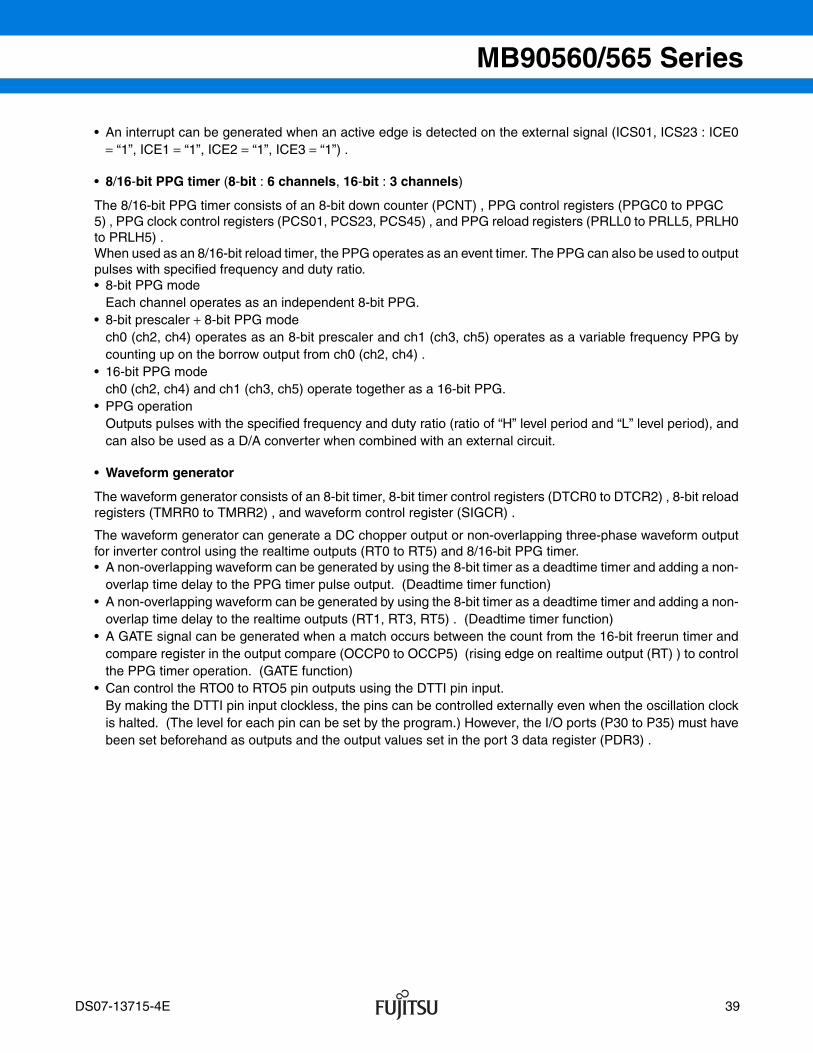
• 8/16-bit PPG timer (8-bit × 6 channels or 16-bit × 3 channels) The period and duty of the output pulse canbe set by the program.
• Waveform generator (8-bit timer : 3 channels) • UART : 2 channels
• Full-duplex, double-buffered (8-bit) • Can be set to asynchronous or clock synchronous serial transfer (I/O expansion serial) operation
• DTP/external interrupt circuit (8 channels) • External interrupts can activate the extended intelligent I/O service.• Generates interrupts in response to external interrupt inputs.
2 DS07-13715-4E
MB90560/565 Series
• Delayed interrupt generation module• Generates an interrupt request for task switching.
• 8/10-bit A/D converter : 8 channels• 8-bit or 10-bit resolution selectable
DS07-13715-4E 3
MB90560/565 Series
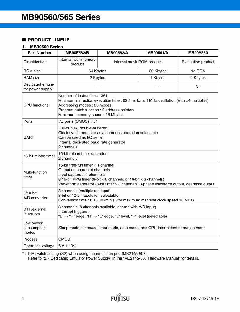
PRODUCT LINEUP1. MB90560 Series
* : DIP switch setting (S2) when using the emulation pod (MB2145-507) .Refer to “2.7 Dedicated Emulator Power Supply” in the “MB2145-507 Hardware Manual” for details.
Part Number MB90F562/B MB90562/A MB90561/A MB90V560
ClassificationInternal flash memory
productInternal mask ROM product Evaluation product
ROM size 64 Kbytes 32 Kbytes No ROM
RAM size 2 Kbytes 1 Kbytes 4 Kbytes
Dedicated emula-tor power supply* ⎯ ⎯ No
CPU functions
Number of instructions : 351Minimum instruction execution time : 62.5 ns for a 4 MHz oscillation (with ×4 multiplier) Addressing modes : 23 modesProgram patch function : 2 address pointersMaximum memory space : 16 Mbytes
Ports I/O ports (CMOS) : 51
UART
Full-duplex, double-bufferedClock synchronous or asynchronous operation selectableCan be used as I/O serialInternal dedicated baud rate generator2 channels
16-bit reload timer16-bit reload timer operation2 channels
Multi-function timer
16-bit free-run timer × 1 channelOutput compare × 6 channelsInput capture × 4 channels8/16-bit PPG timer (8-bit × 6 channels or 16-bit × 3 channels) Waveform generator (8-bit timer × 3 channels) 3-phase waveform output, deadtime output
8/10-bit A/D converter
8 channels (multiplexed input) 8-bit or 10-bit resolution selectableConversion time : 6.13 µs (min.) (for maximum machine clock speed 16 MHz)
DTP/external interrupts
8 channels (8 channels available, shared with A/D input) Interrupt triggers : “L” → “H” edge, “H” → “L” edge, “L” level, “H” level (selectable)
Low power consumption modes
Sleep mode, timebase timer mode, stop mode, and CPU intermittent operation mode
Process CMOS
Operating voltage 5 V ± 10%
4 DS07-13715-4E

MB90560/565 Series
2. MB90565 Series
* : DIP switch setting (S2) when using the emulation pod (MB2145-507) .Refer to “2.7 Dedicated Emulator Power Supply” in the “MB2145-507 Hardware Manual” for details.
Part Number MB90F568 MB90568 MB90567
Classification Internal flash memory product Internal mask ROM product
ROM size 128 Kbytes 96 Kbytes
RAM size 4 Kbytes 4 Kbytes
Dedicated emula-tor power supply* ⎯ ⎯
CPU functions
Number of instructions : 351Minimum instruction execution time : 62.5 ns for a 4 MHz oscillation (with ×4 multiplier) Addressing modes : 23 modesProgram patch function : 2 address pointersMaximum memory space : 16 Mbytes
Ports I/O ports (CMOS) : 51
UART
Full-duplex, double-bufferedClock synchronous or asynchronous operation selectableCan be used as I/O serialInternal dedicated baud rate generator2 channels
16-bit reload timer16-bit reload timer operation2 channels
Multi-function timer
16-bit free-run timer × 1 channelOutput compare × 6 channelsInput capture × 4 channels8/16-bit PPG timer (8-bit × 6 channels or 16-bit × 3 channels) Waveform generator (8-bit timer × 3 channels) 3-phase waveform output, deadtime output
8/10-bit A/D converter
8 channels (multiplexed input) 8-bit or 10-bit resolution selectableConversion time : 6.13 µs (min.) (for maximum machine clock speed 16 MHz)
DTP/external interrupts
8 channels (8 channels available, shared with A/D input) Interrupt triggers : “L” → “H” edge, “H” → “L” edge, “L” level, “H” level (selectable)
Low power con-sumption modes
Sleep mode, timebase timer mode, stop mode, and CPU intermittent operation mode
Process CMOS
Operating voltage 3.3 V ± 0.3 V
DS07-13715-4E 5

MB90560/565 Series
PACKAGE AND CORRESPONDING PRODUCTS
: Available : Not available
Note : See the “Package Dimensions” section for details of each package.
Package MB90561/A MB90562/A MB90F562/B MB90567 MB90568 MB90F568 MB90V560
FPT-64P-M09 (LQFP-0.65 mm)
FPT-64P-M06 (QFP-1.00 mm)
DIP-64P-M01 (SH-DIP)
PGA-256C-A01 (PGA)
×
×
× × × ×
× × × × × ×
×
6 DS07-13715-4E

MB90560/565 Series
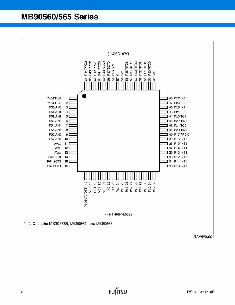
PIN ASSIGNMENTS
(Continued)
(TOP VIEW)
(FPT-64P-M06)
* : N.C. on the MB90F568, MB90567, and MB90568.
P44/PPG3P45/PPG4P46/PPG5
P50/AN0P51/AN1P52/AN2P53/AN3P54/AN4P55/AN5P56/AN6P57/AN7
AVCC
AVRAVSS
P60/SIN1P61/SOT1P62/SCK1
P63/INT7/DTTIMD0
123456789
10111213141516171819
51504948474645444342414039383736353433
P30/RTO0VSS
P27/IN3P26/IN2P25/IN1P24/IN0P23/TO1P22/TIN1P21/TO0P20/TIN0P17/FRCKP16/INT6P15/INT5P14/INT4P13/INT3P12/INT2P11/INT1P10/INT0P07
64 63 62 61 60 59 58 57 56 55 54 53 52
P43
/PP
G2
P42
/PP
G1
P41
/PP
G0
P40
/SC
K0
P37
/SO
T0
P36
/SIN
0C
*
VC
C
P35
/RTO
5P
34/R
TO4
P33
/RTO
3P
32/R
TO2
P31
/RTO
1
20 21 22 23 24 25 26 27 28 29 30 31 32
RS
TM
D1
MD
2X
0X
1V
SS
P00
P01
P02
P03
P04
P05
P06
DS07-13715-4E 7
MB90560/565 Series
(Continued)
(TOP VIEW)
(FPT-64P-M09)
* : N.C. on the MB90F568, MB90567, and MB90568.
P45/PPG4
P46/PPG5
P50/AN0
P51/AN1
P52/AN2
P53/AN3
P54/AN4
P55/AN5
P56/AN6
P57/AN7
AVCC
AVR
AVSS
P60/SIN1
P61/SOT1
P62/SCK1
1
2
3
4
5
6
7
8
9
10
11
12
13
14
15
16
48
47
46
45
44
43
42
41
40
39
38
37
36
35
34
33
P27/IN3
P26/IN2
P25/IN1
P24/IN0
P23/TO1
P22/TIN1
P21/TO0
P20/TIN0
P17/FRCK
P16/INT6
P15/INT5
P14/INT4
P13/INT3
P12/INT2
P11/INT1
P10/INT0
64 63 62 61 60 59 58 57 56 55 54 53 52 51 50 49
P44
/PP
G3
P43
/PP
G2
P42
/PP
G1
P41
/PP
G0
P40
/SC
K0
P37
/SO
T0
P36
/SIN
0
C*
VC
C
P35
/RTO
5
P34
/RTO
4
P33
/RTO
3
P32
/RTO
2
P31
/RTO
1
P30
/RTO
0
VS
S
17 18 19 20 21 22 23 24 25 26 27 28 29 30 31 32
P63
/INT
7/D
TT
I
MD
0
RS
T
MD
1
MD
2
X0
X1
VS
S
P00
P01
P02
P03
P04
P05
P06
P07
8 DS07-13715-4E

MB90560/565 Series
(Continued)
(TOP VIEW)
(DIP-64P-M01) (Only support MB90F562/B, MB90561/A, and MB90562/A.)
* : Not support on the MB90F568, MB90567, and MB90568.
C*
P36/SIN0P37/SOT0P40/SCK0P41/PPG0P42/PPG1P43/PPG2P44/PPG3P45/PPG4P46/PPG5
P50/AN0P51/AN1P52/AN2P53/AN3P54/AN4P55/AN5P56/AN6P57/AN7
AVCC
AVRAVSS
P60/SIN1P61/SOT1P62/SCK1
P63/INT7/DTTIMD0RSTMD1MD2
X0X1
VSS
123456789
1011121314151617181920212223242526272829303132
6463626160595857565554535251504948474645444342414039383736353433
VCC
P35/RTO5P34/RTO4P33/RTO3P32/RTO2P31/RTO1P30/RTO0VSS
P27/IN3P26/IN2P25/IN1P24/IN0P23/TO1P22/TIN1P21/TO0P20/TIN0P17/FRCKP16/INT6P15/INT5P14/INT4P13/INT3P12/INT2P11/INT1P10/INT0P07P06P05P04P03P02P01P00
DS07-13715-4E 9
MB90560/565 Series
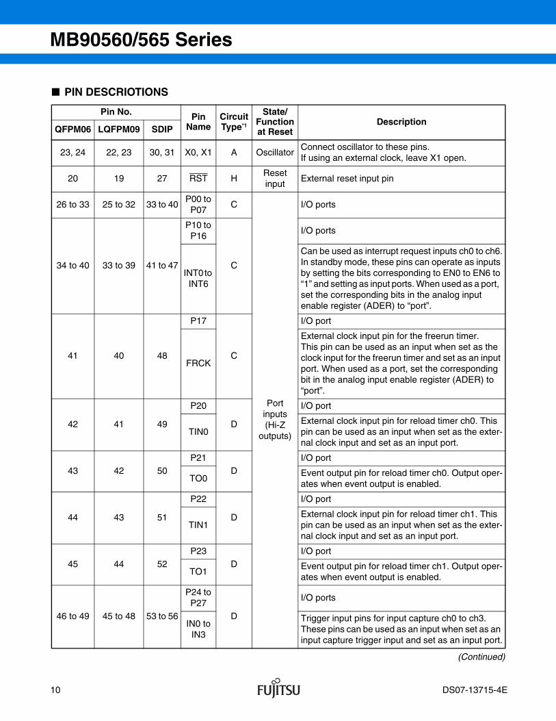
PIN DESCRIOTIONS
(Continued)
Pin No. Pin Name
Circuit Type*1
State/Function at Reset
DescriptionQFPM06 LQFPM09 SDIP
23, 24 22, 23 30, 31 X0, X1 A OscillatorConnect oscillator to these pins.If using an external clock, leave X1 open.
20 19 27 RST HResetinput
External reset input pin
26 to 33 25 to 32 33 to 40P00 to
P07C
Port inputs (Hi-Z
outputs)
I/O ports
34 to 40 33 to 39 41 to 47
P10 to P16
C
I/O ports
INT0 to INT6
Can be used as interrupt request inputs ch0 to ch6.In standby mode, these pins can operate as inputs by setting the bits corresponding to EN0 to EN6 to “1” and setting as input ports. When used as a port, set the corresponding bits in the analog input enable register (ADER) to “port”.
41 40 48
P17
C
I/O port
FRCK
External clock input pin for the freerun timer.This pin can be used as an input when set as the clock input for the freerun timer and set as an input port. When used as a port, set the corresponding bit in the analog input enable register (ADER) to “port”.
42 41 49
P20
D
I/O port
TIN0External clock input pin for reload timer ch0. This pin can be used as an input when set as the exter-nal clock input and set as an input port.
43 42 50P21
DI/O port
TO0Event output pin for reload timer ch0. Output oper-ates when event output is enabled.
44 43 51
P22
D
I/O port
TIN1External clock input pin for reload timer ch1. This pin can be used as an input when set as the exter-nal clock input and set as an input port.
45 44 52P23
DI/O port
TO1Event output pin for reload timer ch1. Output oper-ates when event output is enabled.
46 to 49 45 to 48 53 to 56
P24 to P27
D
I/O ports
IN0 to IN3
Trigger input pins for input capture ch0 to ch3. These pins can be used as an input when set as an input capture trigger input and set as an input port.
10 DS07-13715-4E
Changed the circuit type of RST pin to H.

MB90560/565 Series
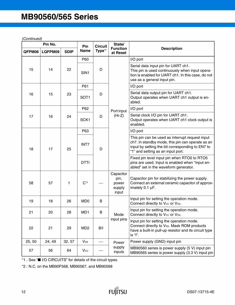
(Continued)
Pin No. Pin Name
Circuit Type*1
State/Function at Reset
DescriptionQFPM06 LQFPM09 SDIP
51 to 56 50 to 55 58 to 63
P30 to P35
E
Portinputs(Hi-Z)
I/O ports
RTO0 to
RTO5
Event output pins for the output compare and waveform generator output pins. The pins output the specified waveform generated by the waveform generator. If not using waveform generation, these terminals enable output compare event output to use as output compare outputs. When used as a port, set the corresponding bits in the analog input enable register (ADER) to “port”.
59 58 2
P36
D
I/O port
SIN0
Serial data input pin for UART ch0.This pin is used continuously when input operation is enabled for UART ch0. In this case, do not use as a general input pin.
60 59 3
P37
D
I/O port
SOT0Serial data output pin for UART ch0.Output operates when UART ch0 output is en-abled.
61 60 4
P40
D
I/O port
SCK0Serial clock I/O pin for UART ch0.Output operates when UART ch0 clock output is enabled.
62 to 64, 1 to 3
61 to 64, 1, 2
5 to 10
P41 to P46
D
I/O ports
PPG0 to
PPG5
Output pins for PPG ch0 to ch5.The outputs operate when output is enabled for PPG ch0 to ch5.
4 to 11 3 to 10 11 to 18
P50 to P57
FAnaloginputs
I/O ports
AN0 to AN7
Analog input pins for the A/D converter. Input is available when the corresponding analog input en-able register bits are set. (ADER : bit0 to bit7)
12 11 19 AVCC ⎯Power supplyinput
VCC power supply input pin for A/D converter.
13 12 20 AVR GRefer-
ence volt-age input
Reference voltage input pin for A/D converter.Ensure that the voltage does not exceed VCC.
14 13 21 AVSS ⎯Power supplyinput
VSS power supply input pin for A/D converter.
DS07-13715-4E 11
MB90560/565 Series
(Continued)
*1 : See “ I/O CIRCUITS” for details of the circuit types.
*2 : N.C. on the MB90F568, MB90567, and MB90568
Pin No. Pin Name
Circuit Type*1
State/Function at Reset
DescriptionQFPM06 LQFPM09 SDIP
15 14 22
P60
D
Port input (Hi-Z)
I/O port
SIN1
Serial data input pin for UART ch1.This pin is used continuously when input opera-tion is enabled for UART ch1. In this case, do not use as a general input pin.
16 15 23
P61
D
I/O port
SOT1Serial data output pin for UART ch1.Output operates when UART ch1 output is en-abled.
17 16 24
P62
D
I/O port
SCK1Serial clock I/O pin for UART ch1.Output operates when UART ch1 clock output is enabled.
18 17 25
P63
D
I/O port
INT7
This pin can be used as interrupt request input ch7. In standby mode, this pin can operate as an input by setting the bit corresponding to EN7 to “1” and setting as an input port.
DTTIFixed pin level input pin when RTO0 to RTO5 pins are used. Input is enabled when “input en-abled” set in the waveform generator.
58 57 1 C*2 ⎯
Capacitor pin,
power supply input
Capacitor pin for stabilizing the power supply. Connect an external ceramic capacitor of approx-imately 0.1 µF.
19 18 26 MD0 B
Modeinput pins
Input pin for setting the operation mode. Connect directly to VCC or VSS.
21 20 28 MD1 BInput pin for setting the operation mode. Connect directly to VCC or VSS.
22 21 29 MD2 B/I
Input pin for setting the operation mode. Connect directly to VSS. Mask ROM products have a built-in pull-up resistor and its circuit type is “I”.
25, 50 24, 49 32, 57 VSS ⎯ Power supplyinputs
Power supply (GND) input pin
57 56 64 VCC ⎯ MB90560 series is power supply (5 V) input pinMB90565 series is power supply (3.3 V) input pin
12 DS07-13715-4E
Changed the circuit type of MD2 pin to B/I. Changed the “Description” of MD2 pin.
MB90560/565 Series
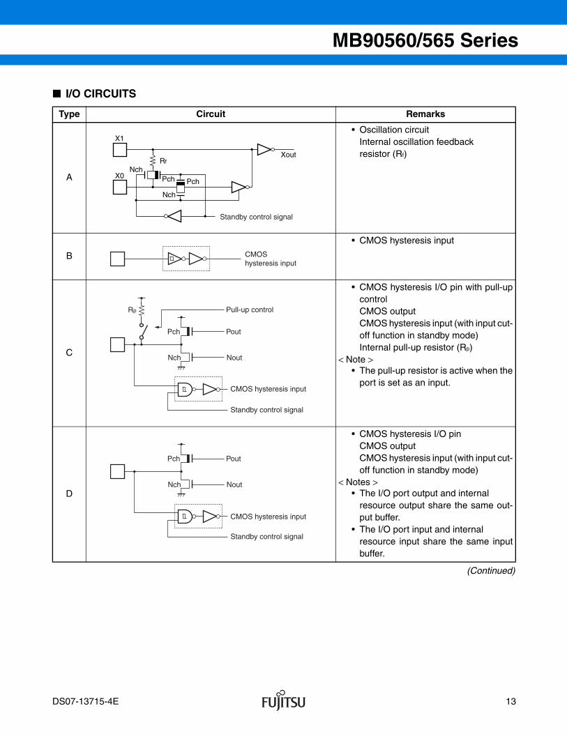
I/O CIRCUITS
(Continued)
Type Circuit Remarks
A
• Oscillation circuitInternal oscillation feedback resistor (Rf)
B
• CMOS hysteresis input
C
• CMOS hysteresis I/O pin with pull-upcontrolCMOS outputCMOS hysteresis input (with input cut-off function in standby mode) Internal pull-up resistor (Rp)
< Note > • The pull-up resistor is active when the
port is set as an input.
D
• CMOS hysteresis I/O pinCMOS outputCMOS hysteresis input (with input cut-off function in standby mode)
< Notes > • The I/O port output and internal
resource output share the same out-put buffer.
• The I/O port input and internalresource input share the same inputbuffer.
X1
Xout
X0
Rf
Nch
Nch
Pch Pch
Standby control signal
CMOS hysteresis input
Rp
Pout
Pull-up control
Nout
CMOS hysteresis input
Standby control signal
Pch
Nch
Pout
Nout
CMOS hysteresis input
Standby control signal
Pch
Nch
DS07-13715-4E 13
MB90560/565 Series
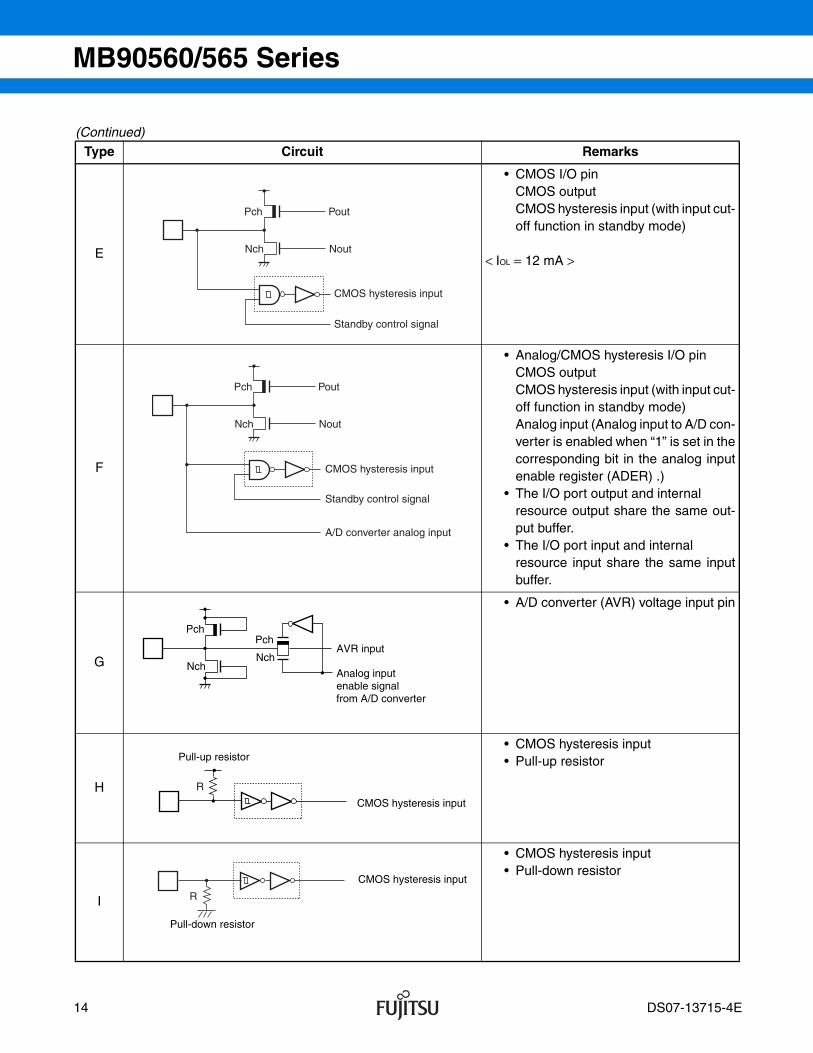
(Continued)
Type Circuit Remarks
E
• CMOS I/O pinCMOS outputCMOS hysteresis input (with input cut-off function in standby mode)
< IOL = 12 mA >
F
• Analog/CMOS hysteresis I/O pinCMOS outputCMOS hysteresis input (with input cut-off function in standby mode) Analog input (Analog input to A/D con-verter is enabled when “1” is set in thecorresponding bit in the analog inputenable register (ADER) .)
• The I/O port output and internal resource output share the same out-put buffer.
• The I/O port input and internal resource input share the same inputbuffer.
G
• A/D converter (AVR) voltage input pin
H
• CMOS hysteresis input• Pull-up resistor
I
• CMOS hysteresis input• Pull-down resistor
Pout
Nout
CMOS hysteresis input
Standby control signal
Pch
Nch
Pout
Nout
CMOS hysteresis input
Standby control signal
A/D converter analog input
Pch
Nch
Pch
Nch
PchAVR input
Analog inputenable signalfrom A/D converter
Nch
R
CMOS hysteresis input
Pull-up resistor
R
CMOS hysteresis input
Pull-down resistor
14 DS07-13715-4E
asatani
ノート
asatani : Marked
線
Added the Type H and Type I.
MB90560/565 Series
HANDLING DEVICESTake note of the following nine points when handling devices : • Do not exceed maximum rated voltage (to prevent latch-up) • Supply voltage stability• Power-on precautions• Treatment of unused pins• Treatment of A/D converter power supply pins• Notes on using an external clock• Power supply pins• Sequence for connecting and disconnecting the A/D converter power supply and analog input pins• Notes on using the DIV A, Ri and DIVW A, RWi instructions
• Device Handling Precautions
(1) Do not exceed maximum rated voltage (to prevent latch-up)
Do not apply a voltage grater than VCC or less than VSS to the MB90560/565 series input or output pins. Alsoensure that the voltage between VCC and VSS does not exceed the rating. Applying a voltage in excess of theratings may result in latch-up causing thermal damage to circuit elements.
Similarly, when connecting or disconnecting the power to the analog power supply (AVCC, AVR) and analoginputs (AN0 to AN7) , ensure that the analog power supply voltages do not exceed the digital voltage (VCC) .
(2) Supply voltage stability
Rapid changes in the VCC supply voltage may cause the device to misoperate. Accordingly, ensure that the VCC
power supply is stable. The standard for power supply voltage stability is a peak-to-peak VCC ripple voltage atthe supply frequency (50 to 60 Hz) of 10% or less of VCC and a transient fluctuation in the voltage of 0.1 V/msor less when turning the power supply on or off.
(3) Power-on precautions
To prevent misoperation of the internal regulator circuit, ensure that the voltage rise time at power-on is at least50 µs (between 0.2 V to 2.7 V) .
(4) Treatment of unused pins
Leaving unused input pins unconnected can cause misoperation or permanent damage to the device due tolatchup. Always pull-up or pull-down unused pins using a 2 kΩ or larger resistor.
If some I/O pins are unused, either set as outputs and leave open circuit or set as inputs and treat in the sameway as input pins.
(5) Treatment of A/D converter power supply pins
If not using the A/D converter, connect the analog power supply pins so that AVCC = AVR = VCC and AVSS = VSS.
(6) Notes on using an external clock
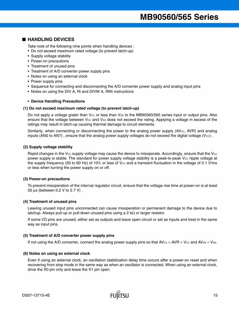
Even if using an external clock, an oscillation stabilization delay time occurs after a power-on reset and whenrecovering from stop mode in the same way as when an oscillator is connected. When using an external clock,drive the X0 pin only and leave the X1 pin open.
DS07-13715-4E 15
MB90560/565 Series
Example of using an external clock
(7) Power supply pins
The multiple VCC and VSS pins are connected together in the internal device design so as to prevent misoperationsuch as latch-up. However, always connect all VCC and VSS pins to the same potential externally to minimizespurious radiation, prevent misoperation of strobe signals due to increases in the ground level, and maintain theoverall output current rating.
Also, ensure that the impedance of the VCC and VSS connections to the power supply is as low as possible.To minimize these problems, connect a bypass capacitor of approximately 0.1 µF between VCC and VSS. Connectthe capacitor close to the VCC and VSS pins.
(8) Sequence for connecting and disconnecting power supply
Do not apply voltage to the A/D converter power supply pins (AVCC, AVR, AVSS) or analog inputs (AN0 to AN7)until the digital power supply (VCC) is turned on. When turning the device off, turn off the digital power supplyafter disconnecting the A/D converter power supply and analog inputs. When turning the power on or off, ensurethat AVR does not exceed AVCC.
When using the I/O ports that share pins with the analog inputs, ensure that the input voltage does not exceedAVCC (turning the analog and digital power supplies on and off simultaneously is OK) .
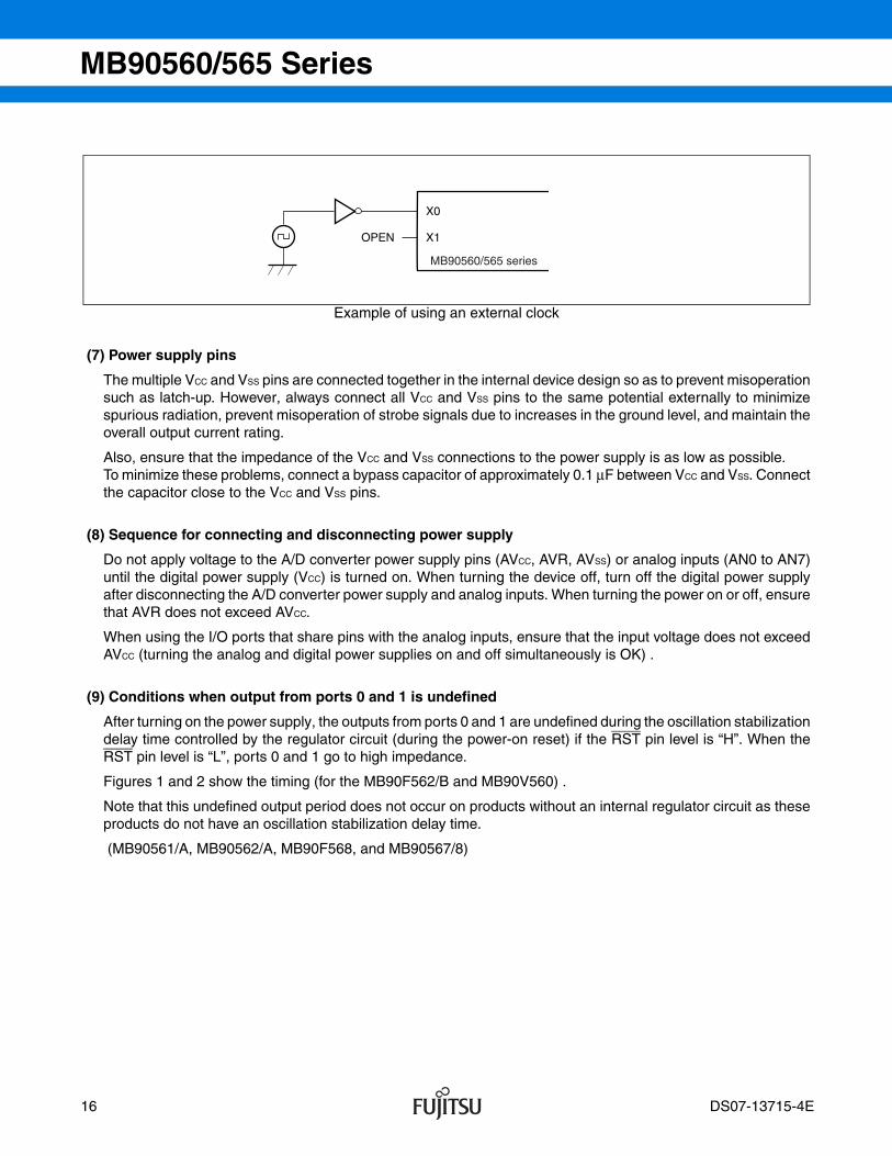
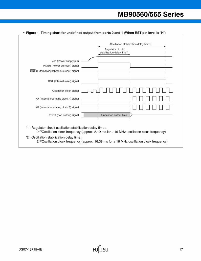
(9) Conditions when output from ports 0 and 1 is undefined
After turning on the power supply, the outputs from ports 0 and 1 are undefined during the oscillation stabilizationdelay time controlled by the regulator circuit (during the power-on reset) if the RST pin level is “H”. When theRST pin level is “L”, ports 0 and 1 go to high impedance.
Figures 1 and 2 show the timing (for the MB90F562/B and MB90V560) .
Note that this undefined output period does not occur on products without an internal regulator circuit as theseproducts do not have an oscillation stabilization delay time.
(MB90561/A, MB90562/A, MB90F568, and MB90567/8)
X0
X1OPEN
MB90560/565 series
16 DS07-13715-4E
MB90560/565 Series
• Figure 1 Timing chart for undefined output from ports 0 and 1 (When RST pin level is “H”)
Oscillation stabilization delay time*2
Regulator circuitstabilization delay time*1
VCC (Power supply pin)
PONR (Power-on reset) signal
RST (External asynchronous reset) signal
RST (Internal reset) signal
Oscillation clock signal
KA (Internal operating clock A) signal
KB (Internal operating clock B) signal
PORT (port output) signal Undefined output time
*1 : Regulator circuit oscillation stabilization delay time : 217/Oscillation clock frequency (approx. 8.19 ms for a 16 MHz oscillation clock frequency)
*2 : Oscillation stabilization delay time : 218/Oscillation clock frequency (approx. 16.38 ms for a 16 MHz oscillation clock frequency)
DS07-13715-4E 17
MB90560/565 Series
• Figure 2 Timing chart for ports 0 and 1 going to high impedance state (When RST pin level is “L”)
(10) Notes on using the DIV A, Ri and DIVW A, RWi instructions
The location in which the remainder value produced by the signed division instructions “DIV A, Ri” and “DIVWA, RWi” is stored depends on the bank register. The remainder is stored in an address in the memory bankspecified in the bank register.
Set the bank register to “00H” when using the “DIV A, Ri” and “DIVW A, RWi” instructions.
(11) Notes on using REALOS
The extended intelligent I/O service (EI2OS) cannot be used when using REALOS.
(12) Caution on Operations during PLL Clock Mode
If the PLL clock mode is selected in the microcontroller, it may attempt to continue the operation using the free-running frequency of the self oscillation circuit in the PLL circuitry even if the oscillator is out of place or the clockinput is stopped. Performance of this operation, however, cannot be guaranteed.
Oscillation stabilization delay time*2
Regulator circuitstabilization delay time*1
VCC (Power supply pin)
PONR (Power-on reset) signal
RST (External asynchronous reset) signal
RST (Internal reset) signal
Oscillation clock signal
KA (Internal operating clock A) signal
KB (Internal operating clock B) signal
PORT (port output) signalHigh impedance
*1 : Regulator circuit oscillation stabilization delay time : 217/Oscillation clock frequency (approx. 8.19 ms for a 16 MHz oscillation clock frequency)
*2 : Oscillation stabilization delay time : 218/Oscillation clock frequency (approx. 16.38 ms for a 16 MHz oscillation clock frequency)
18 DS07-13715-4E

MB90560/565 Series
BLOCK DIAGRAM
F2MC-16LXCPU
RAM
ROM
UARTch0
UARTch1
P00
P07
P10
P17
P20
P27
P30
P37
P40
P46
P50
P57
P60
P63
X0, X1RST
MD0 to MD2
SIN0SOT0SCK0
SIN1SOT1SCK1
INT0 to INT7
AVCC
AVRAVSS
AN0 to AN7
TO1TIN1
TO0TIN0
PPG0 to PPG5
FRCK
IN0 to IN3
RTO0RTO1RTO2RTO3RTO4RTO5DTTI
Clockcontrol circuit
Interrupt controller
8/16-bitPPG timerch0 to ch5*
Inputcapture
ch0 to ch3
16-bitfreeruntimer
Outputcompare
ch0 to ch5
Waveform generator circuit
8/10-bitA/D converter
16-bitreload timer
ch0
16-bitreload timer
ch1
DTP/external interrupts
Inte
rnal
dat
a bu
s
I/O ports (Ports 0, 1, 2, 3, 4, 5, and 6)
* : Channel numbers when used as 8-bit timers. Three channels (ch1, ch3, and ch5) are available when used as 16-bit timers.
Note: The I/O ports share pins with the various peripheral functions (resources) .See the Pin Assignment and Pin Description sections for details.Note that, if a pin is used by a peripheral function (resource) , it may not be used as an I/O port.
DS07-13715-4E 19
MB90560/565 Series
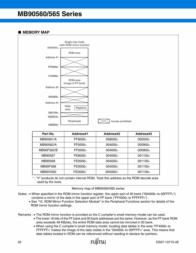
MEMORY MAP
Memory map of MB90560/565 series
Notes : • When specified in the ROM mirror function register, the upper part of 00 bank (“004000H to 00FFFFH”) contains a mirror of the data in the upper part of FF bank (“FF4000H to FFFFFFH”) .
• See “10. ROM Mirror Function Selection Module” in the Peripheral Functions section for details of the ROM mirror function settings.
Remarks : • The ROM mirror function is provided so the C compiler’s small memory model can be used.• The lower 16 bits of the FF bank and 00 bank addresses are the same. However, as the FF bank ROM
area exceeds 48 KBytes, the entire ROM data area cannot be mirrored in 00 bank.• When using the C compiler’s small memory model, locating data tables in the area “FF4000H to
FFFFFFH” makes the image of the data visible in the “004000H to 00FFFFH” area. This means that data tables located in ROM can be referenced without needing to declare far pointers.
FFFFFFH
FF0000H
010000H
004000H
000100H
0000C0H
000000H
Single chip mode(with ROM mirror function)
ROM area
Address #1
ROM area(image of FF bank)
Address #2
Address #3RAMarea
Registers
Peripherals Access prohibited
* : “V” products do not contain internal ROM. Treat this address as the ROM decode area used by the tools.
Part No. Address#1 Address#2 Address#3
MB90561/A FF8000H 008000H 000500H
MB90562/A FF0000H 004000H 000900H
MB90F562/B FF0000H 004000H 000900H
MB90567 FE8000H 004000H 001100H
MB90568 FE0000H 004000H 001100H
MB90F568 FE0000H 004000H 001100H
MB90V560 FE0000H* 004000H* 001100H
20 DS07-13715-4E
MB90560/565 Series
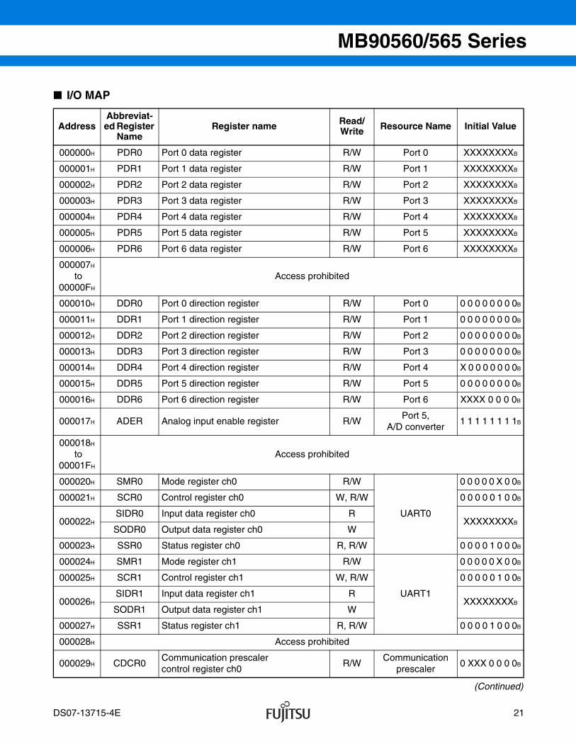
I/O MAP
(Continued)
AddressAbbreviat-ed Register
NameRegister name Read/
Write Resource Name Initial Value
000000H PDR0 Port 0 data register R/W Port 0 XXXXXXXXB
000001H PDR1 Port 1 data register R/W Port 1 XXXXXXXXB
000002H PDR2 Port 2 data register R/W Port 2 XXXXXXXXB
000003H PDR3 Port 3 data register R/W Port 3 XXXXXXXXB
000004H PDR4 Port 4 data register R/W Port 4 XXXXXXXXB
000005H PDR5 Port 5 data register R/W Port 5 XXXXXXXXB
000006H PDR6 Port 6 data register R/W Port 6 XXXXXXXXB
000007H
to 00000FH
Access prohibited
000010H DDR0 Port 0 direction register R/W Port 0 0 0 0 0 0 0 0 0B
000011H DDR1 Port 1 direction register R/W Port 1 0 0 0 0 0 0 0 0B
000012H DDR2 Port 2 direction register R/W Port 2 0 0 0 0 0 0 0 0B
000013H DDR3 Port 3 direction register R/W Port 3 0 0 0 0 0 0 0 0B
000014H DDR4 Port 4 direction register R/W Port 4 X 0 0 0 0 0 0 0B
000015H DDR5 Port 5 direction register R/W Port 5 0 0 0 0 0 0 0 0B
000016H DDR6 Port 6 direction register R/W Port 6 XXXX 0 0 0 0B
000017H ADER Analog input enable register R/WPort 5,
A/D converter1 1 1 1 1 1 1 1B
000018H
to 00001FH
Access prohibited
000020H SMR0 Mode register ch0 R/W
UART0
0 0 0 0 0 X 0 0B
000021H SCR0 Control register ch0 W, R/W 0 0 0 0 0 1 0 0B
000022HSIDR0 Input data register ch0 R
XXXXXXXXBSODR0 Output data register ch0 W
000023H SSR0 Status register ch0 R, R/W 0 0 0 0 1 0 0 0B
000024H SMR1 Mode register ch1 R/W
UART1
0 0 0 0 0 X 0 0B
000025H SCR1 Control register ch1 W, R/W 0 0 0 0 0 1 0 0B
000026HSIDR1 Input data register ch1 R
XXXXXXXXBSODR1 Output data register ch1 W
000027H SSR1 Status register ch1 R, R/W 0 0 0 0 1 0 0 0B
000028H Access prohibited
000029H CDCR0Communication prescalercontrol register ch0
R/WCommunication
prescaler0 XXX 0 0 0 0B
DS07-13715-4E 21
MB90560/565 Series
(Continued)
AddressAbbreviat-ed Register
NameRegister name Read/
Write Resource Name Initial Value
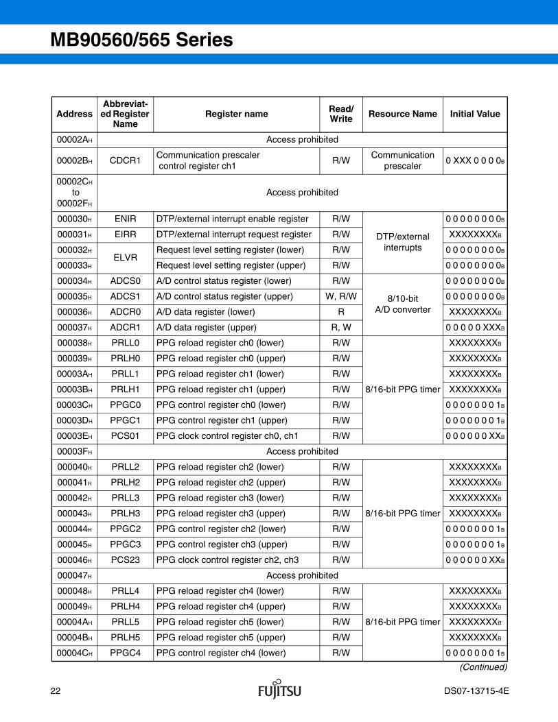
00002AH Access prohibited
00002BH CDCR1Communication prescaler control register ch1
R/WCommunication
prescaler0 XXX 0 0 0 0B
00002CH
to 00002FH
Access prohibited
000030H ENIR DTP/external interrupt enable register R/W
DTP/externalinterrupts
0 0 0 0 0 0 0 0B
000031H EIRR DTP/external interrupt request register R/W XXXXXXXXB
000032HELVR
Request level setting register (lower) R/W 0 0 0 0 0 0 0 0B
000033H Request level setting register (upper) R/W 0 0 0 0 0 0 0 0B
000034H ADCS0 A/D control status register (lower) R/W
8/10-bitA/D converter
0 0 0 0 0 0 0 0B
000035H ADCS1 A/D control status register (upper) W, R/W 0 0 0 0 0 0 0 0B
000036H ADCR0 A/D data register (lower) R XXXXXXXXB
000037H ADCR1 A/D data register (upper) R, W 0 0 0 0 0 XXXB
000038H PRLL0 PPG reload register ch0 (lower) R/W
8/16-bit PPG timer
XXXXXXXXB
000039H PRLH0 PPG reload register ch0 (upper) R/W XXXXXXXXB
00003AH PRLL1 PPG reload register ch1 (lower) R/W XXXXXXXXB
00003BH PRLH1 PPG reload register ch1 (upper) R/W XXXXXXXXB
00003CH PPGC0 PPG control register ch0 (lower) R/W 0 0 0 0 0 0 0 1B
00003DH PPGC1 PPG control register ch1 (upper) R/W 0 0 0 0 0 0 0 1B
00003EH PCS01 PPG clock control register ch0, ch1 R/W 0 0 0 0 0 0 XXB
00003FH Access prohibited
000040H PRLL2 PPG reload register ch2 (lower) R/W
8/16-bit PPG timer
XXXXXXXXB
000041H PRLH2 PPG reload register ch2 (upper) R/W XXXXXXXXB
000042H PRLL3 PPG reload register ch3 (lower) R/W XXXXXXXXB
000043H PRLH3 PPG reload register ch3 (upper) R/W XXXXXXXXB
000044H PPGC2 PPG control register ch2 (lower) R/W 0 0 0 0 0 0 0 1B
000045H PPGC3 PPG control register ch3 (upper) R/W 0 0 0 0 0 0 0 1B
000046H PCS23 PPG clock control register ch2, ch3 R/W 0 0 0 0 0 0 XXB
000047H Access prohibited
000048H PRLL4 PPG reload register ch4 (lower) R/W
8/16-bit PPG timer
XXXXXXXXB
000049H PRLH4 PPG reload register ch4 (upper) R/W XXXXXXXXB
00004AH PRLL5 PPG reload register ch5 (lower) R/W XXXXXXXXB
00004BH PRLH5 PPG reload register ch5 (upper) R/W XXXXXXXXB
00004CH PPGC4 PPG control register ch4 (lower) R/W 0 0 0 0 0 0 0 1B
22 DS07-13715-4E
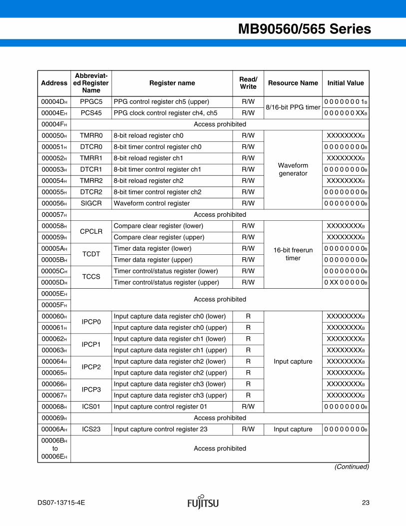
MB90560/565 Series
(Continued)
AddressAbbreviat-ed Register
NameRegister name Read/
Write Resource Name Initial Value
00004DH PPGC5 PPG control register ch5 (upper) R/W8/16-bit PPG timer
0 0 0 0 0 0 0 1B
00004EH PCS45 PPG clock control register ch4, ch5 R/W 0 0 0 0 0 0 XXB
00004FH Access prohibited
000050H TMRR0 8-bit reload register ch0 R/W
Waveformgenerator
XXXXXXXXB
000051H DTCR0 8-bit timer control register ch0 R/W 0 0 0 0 0 0 0 0B
000052H TMRR1 8-bit reload register ch1 R/W XXXXXXXXB
000053H DTCR1 8-bit timer control register ch1 R/W 0 0 0 0 0 0 0 0B
000054H TMRR2 8-bit reload register ch2 R/W XXXXXXXXB
000055H DTCR2 8-bit timer control register ch2 R/W 0 0 0 0 0 0 0 0B
000056H SIGCR Waveform control register R/W 0 0 0 0 0 0 0 0B
000057H Access prohibited
000058HCPCLR
Compare clear register (lower) R/W
16-bit freeruntimer
XXXXXXXXB
000059H Compare clear register (upper) R/W XXXXXXXXB
00005AHTCDT
Timer data register (lower) R/W 0 0 0 0 0 0 0 0B
00005BH Timer data register (upper) R/W 0 0 0 0 0 0 0 0B
00005CHTCCS
Timer control/status register (lower) R/W 0 0 0 0 0 0 0 0B
00005DH Timer control/status register (upper) R/W 0 XX 0 0 0 0 0B
00005EHAccess prohibited
00005FH
000060HIPCP0
Input capture data register ch0 (lower) R
Input capture
XXXXXXXXB
000061H Input capture data register ch0 (upper) R XXXXXXXXB
000062HIPCP1
Input capture data register ch1 (lower) R XXXXXXXXB
000063H Input capture data register ch1 (upper) R XXXXXXXXB
000064HIPCP2
Input capture data register ch2 (lower) R XXXXXXXXB
000065H Input capture data register ch2 (upper) R XXXXXXXXB
000066HIPCP3
Input capture data register ch3 (lower) R XXXXXXXXB
000067H Input capture data register ch3 (upper) R XXXXXXXXB
000068H ICS01 Input capture control register 01 R/W 0 0 0 0 0 0 0 0B
000069H Access prohibited
00006AH ICS23 Input capture control register 23 R/W Input capture 0 0 0 0 0 0 0 0B
00006BH
to 00006EH
Access prohibited
DS07-13715-4E 23
MB90560/565 Series
(Continued)
AddressAbbreviat-ed Register
NameRegister name Read/
Write Resource Name Initial Value
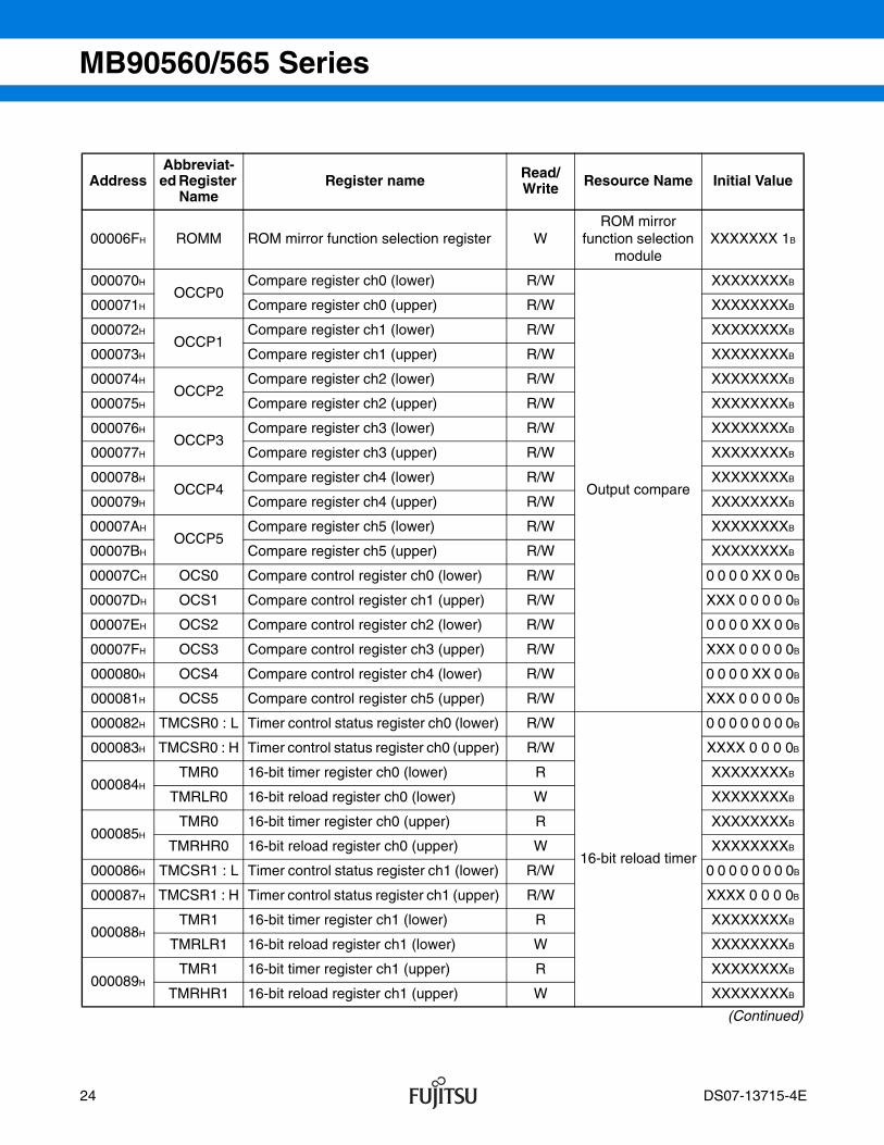
00006FH ROMM ROM mirror function selection register WROM mirror
function selection module
XXXXXXX 1B
000070HOCCP0
Compare register ch0 (lower) R/W
Output compare
XXXXXXXXB
000071H Compare register ch0 (upper) R/W XXXXXXXXB
000072HOCCP1
Compare register ch1 (lower) R/W XXXXXXXXB
000073H Compare register ch1 (upper) R/W XXXXXXXXB
000074HOCCP2
Compare register ch2 (lower) R/W XXXXXXXXB
000075H Compare register ch2 (upper) R/W XXXXXXXXB
000076HOCCP3
Compare register ch3 (lower) R/W XXXXXXXXB
000077H Compare register ch3 (upper) R/W XXXXXXXXB
000078HOCCP4
Compare register ch4 (lower) R/W XXXXXXXXB
000079H Compare register ch4 (upper) R/W XXXXXXXXB
00007AHOCCP5
Compare register ch5 (lower) R/W XXXXXXXXB
00007BH Compare register ch5 (upper) R/W XXXXXXXXB
00007CH OCS0 Compare control register ch0 (lower) R/W 0 0 0 0 XX 0 0B
00007DH OCS1 Compare control register ch1 (upper) R/W XXX 0 0 0 0 0B
00007EH OCS2 Compare control register ch2 (lower) R/W 0 0 0 0 XX 0 0B
00007FH OCS3 Compare control register ch3 (upper) R/W XXX 0 0 0 0 0B
000080H OCS4 Compare control register ch4 (lower) R/W 0 0 0 0 XX 0 0B
000081H OCS5 Compare control register ch5 (upper) R/W XXX 0 0 0 0 0B
000082H TMCSR0 : L Timer control status register ch0 (lower) R/W
16-bit reload timer
0 0 0 0 0 0 0 0B
000083H TMCSR0 : H Timer control status register ch0 (upper) R/W XXXX 0 0 0 0B
000084HTMR0 16-bit timer register ch0 (lower) R XXXXXXXXB
TMRLR0 16-bit reload register ch0 (lower) W XXXXXXXXB
000085HTMR0 16-bit timer register ch0 (upper) R XXXXXXXXB
TMRHR0 16-bit reload register ch0 (upper) W XXXXXXXXB
000086H TMCSR1 : L Timer control status register ch1 (lower) R/W 0 0 0 0 0 0 0 0B
000087H TMCSR1 : H Timer control status register ch1 (upper) R/W XXXX 0 0 0 0B
000088HTMR1 16-bit timer register ch1 (lower) R XXXXXXXXB
TMRLR1 16-bit reload register ch1 (lower) W XXXXXXXXB
000089HTMR1 16-bit timer register ch1 (upper) R XXXXXXXXB
TMRHR1 16-bit reload register ch1 (upper) W XXXXXXXXB
24 DS07-13715-4E
MB90560/565 Series
(Continued)
AddressAbbreviat-ed Register
NameRegister name Read/
Write Resource Name Initial Value
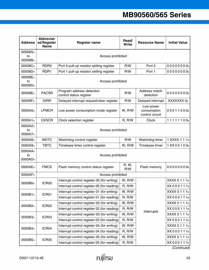
00008AH
to 00008BH
Access prohibited
00008CH RDR0 Port 0 pull-up resistor setting register R/W Port 0 0 0 0 0 0 0 0 0B
00008DH RDR1 Port 1 pull-up resistor setting register R/W Port 1 0 0 0 0 0 0 0 0B
00008EH
to 00009DH
Access prohibited
00009EH PACSRProgram address detectioncontrol status register
R/WAddress match
detection0 0 0 0 0 0 0 0B
00009FH DIRR Delayed interrupt request/clear register R/W Delayed interrupt XXXXXXX 0B
0000A0H LPMCR Low power consumption mode register W, R/WLow power
consumptioncontrol circuit
0 0 0 1 1 0 0 0B
0000A1H CKSCR Clock selection register R, R/W Clock 1 1 1 1 1 1 0 0B
0000A2H
to 0000A7H
Access prohibited
0000A8H WDTC Watchdog control register R/W Watchdog timer 1 XXXX 1 1 1B
0000A9H TBTC Timebase timer control register W, R/W Timebase timer 1 XX 0 0 1 0 0B
0000AAH
to 0000ADH
Access prohibited
0000AEH FMCS Flash memory control status registerR, W, R/W
Flash memory 0 0 0 0 0 0 0 0B
0000AFH Access prohibited
0000B0H ICR00Interrupt control register 00 (for writing) W, R/W
Interrupts
XXXX 0 1 1 1B
Interrupt control register 00 (for reading) R, R/W XX 0 0 0 1 1 1B
0000B1H ICR01Interrupt control register 01 (for writing) W, R/W XXXX 0 1 1 1B
Interrupt control register 01 (for reading) R, R/W XX 0 0 0 1 1 1B
0000B2H ICR02Interrupt control register 02 (for writing) W, R/W XXXX 0 1 1 1B
Interrupt control register 02 (for reading) R, R/W XX 0 0 0 1 1 1B
0000B3H ICR03Interrupt control register 03 (for writing) W, R/W XXXX 0 1 1 1B
Interrupt control register 03 (for reading) R, R/W XX 0 0 0 1 1 1B
0000B4H ICR04Interrupt control register 04 (for writing) W, R/W XXXX 0 1 1 1B
Interrupt control register 04 (for reading) R, R/W XX 0 0 0 1 1 1B
0000B5H ICR05Interrupt control register 05 (for writing) W, R/W XXXX 0 1 1 1B
Interrupt control register 05 (for reading) R, R/W XX 0 0 0 1 1 1B
DS07-13715-4E 25
MB90560/565 Series
(Continued)
AddressAbbreviat-ed Register
NameRegister name Read/
Write Resource Name Initial Value
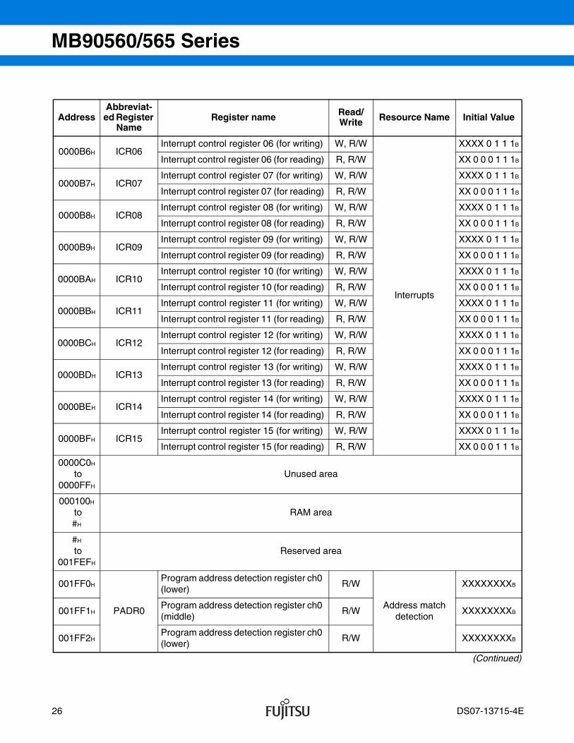
0000B6H ICR06Interrupt control register 06 (for writing) W, R/W
Interrupts
XXXX 0 1 1 1B
Interrupt control register 06 (for reading) R, R/W XX 0 0 0 1 1 1B
0000B7H ICR07Interrupt control register 07 (for writing) W, R/W XXXX 0 1 1 1B
Interrupt control register 07 (for reading) R, R/W XX 0 0 0 1 1 1B
0000B8H ICR08Interrupt control register 08 (for writing) W, R/W XXXX 0 1 1 1B
Interrupt control register 08 (for reading) R, R/W XX 0 0 0 1 1 1B
0000B9H ICR09Interrupt control register 09 (for writing) W, R/W XXXX 0 1 1 1B
Interrupt control register 09 (for reading) R, R/W XX 0 0 0 1 1 1B
0000BAH ICR10Interrupt control register 10 (for writing) W, R/W XXXX 0 1 1 1B
Interrupt control register 10 (for reading) R, R/W XX 0 0 0 1 1 1B
0000BBH ICR11Interrupt control register 11 (for writing) W, R/W XXXX 0 1 1 1B
Interrupt control register 11 (for reading) R, R/W XX 0 0 0 1 1 1B
0000BCH ICR12Interrupt control register 12 (for writing) W, R/W XXXX 0 1 1 1B
Interrupt control register 12 (for reading) R, R/W XX 0 0 0 1 1 1B
0000BDH ICR13Interrupt control register 13 (for writing) W, R/W XXXX 0 1 1 1B
Interrupt control register 13 (for reading) R, R/W XX 0 0 0 1 1 1B
0000BEH ICR14Interrupt control register 14 (for writing) W, R/W XXXX 0 1 1 1B
Interrupt control register 14 (for reading) R, R/W XX 0 0 0 1 1 1B
0000BFH ICR15Interrupt control register 15 (for writing) W, R/W XXXX 0 1 1 1B
Interrupt control register 15 (for reading) R, R/W XX 0 0 0 1 1 1B
0000C0H
to 0000FFH
Unused area
000100H
to #H
RAM area
#H
to 001FEFH
Reserved area
001FF0H
PADR0
Program address detection register ch0 (lower)
R/W
Address match detection
XXXXXXXXB
001FF1HProgram address detection register ch0 (middle)
R/W XXXXXXXXB
001FF2HProgram address detection register ch0 (lower)
R/W XXXXXXXXB
26 DS07-13715-4E

MB90560/565 Series
(Continued)
• Read/write notation
• Initial value notation
AddressAbbreviat-ed Register
NameRegister name Read/
Write Resource Name Initial Value
001FF3H
PADR1
Program address detection register ch1 (lower)
R/W
Address match detection
XXXXXXXXB
001FF4HProgram address detection register ch1 (middle)
R/W XXXXXXXXB
001FF5HProgram address detection register ch1 (lower)
R/W XXXXXXXXB
001FF6H
to 001FFFH
Unused area
R/W : Reading and writing permittedR : Read-onlyW : Write-only
0 : Initial value is “0”.1 : Initial value is “1”.X : Initial value is undefined.
DS07-13715-4E 27

MB90560/565 Series
INTERRUPTS, INTERRUT VECTORS, AND INTERRUPT CONTROL REGISTERS
InterruptEI2OS Sup-port
Interrupt Vector Interrupt Control Register Priori-
tyNo.* Address ICR Address
Reset #08 08H FFFFDCH ⎯ ⎯ High
INT 9 instruction #09 09H FFFFD8H ⎯ ⎯
Exception #10 0AH FFFFD4H ⎯ ⎯
A/D converter conversion complete #11 0BH FFFFD0H ICR00 0000B0H
Output compare channel 0 match #13 0DH FFFFC8HICR01 0000B1H
8/16-bit PPG timer 0 counter borrow #14 0EH FFFFC4H
Output compare channel 1 match #15 0FH FFFFC0HICR02 0000B2H
8/16-bit PPG timer 1 counter borrow #16 10H FFFFBCH
Output compare channel 2 match #17 11H FFFFB8HICR03 0000B3H
8/16-bit PPG timer 2 counter borrow #18 12H FFFFB4H
Output compare channel 3 match #19 13H FFFFB0HICR04 0000B4H
8/16-bit PPG timer 3 counter borrow #20 14H FFFFACH
Output compare channel 4 match #21 15H FFFFA8HICR05 0000B5H
8/16-bit PPG timer 4 counter borrow #22 16H FFFFA4H
Output compare channel 5 match #23 17H FFFFA0HICR06 0000B6H
8/16-bit PPG timer 5 counter borrow #24 18H FFFF9CH
DTP/external interrupt channel 0/1 detection #25 19H FFFF98HICR07 0000B7H
DTP/external interrupt channel 2/3 detection #26 1AH FFFF94H
DTP/external interrupt channel 4/5 detection #27 1BH FFFF90HICR08 0000B8H
DTP/external interrupt channel 6/7 detection #28 1CH FFFF8CH
8-bit timer 0/1/2 counter borrow #29 1DH FFFF88HICR09 0000B9H
16-bit reload timer 0 underflow #30 1EH FFFF84H
16-bit freerun timer overflow #31 1FH FFFF80HICR10 0000BAH
16-bit reload timer 1 underflow #32 20H FFFF7CH
Input capture channel 0/1 #33 21H FFFF78HICR11 0000BBH
16-bit freerun timer clear #34 22H FFFF74H
Input capture channel 2/3 #35 23H FFFF70HICR12 0000BCH
Timebase timer #36 24H FFFF6CH
UART1 receive #37 25H FFFF68HICR13 0000BDH
UART1 send #38 26H FFFF64H
UART0 receive #39 27H FFFF60HICR14 0000BEH
UART0 send #40 28H FFFF5CH
Flash memory status #41 29H FFFF58HICR15 0000BFH
Delay interrupt output module #42 2AH FFFF54H Low
×
×
×
×
×
×
×
×
×
28 DS07-13715-4E

MB90560/565 Series
: Supported
: Not supported
: Supported, includes EI2OS stop function
: Available if the interrupt that shares the same ICR is not used.
* : If two or more interrupts with the same level occur simultaneously, the interrupt with the lower interrupt vector number has priority
×
DS07-13715-4E 29

MB90560/565 Series
PERIPHERAL FUNCTIONS1. I/O Ports
• The I/O ports can be used as general-purpose I/O ports (parallel I/O ports) . The MB90560/565 series have7 ports (51 pins) . The ports share pins with the inputs and outputs of the peripheral functions.
• The port data registers (PDR) are used to output data to the I/O pins and read the data input from the I/Oports. Similarly, the port direction registers (DDR) set the I/O direction (input or output) for each individual portbit.
• The following table lists the I/O ports and the peripheral functions with which they share pins.
Notes : • Pins P30 to P35 of port 3 can drive a maximum of IOL = 12 mA.• Port 5 shares pins with the analog inputs. When using port 5 pins as a general-purpose ports, ensure that the corresponding analog input enable register (ADER) bits are set to “0B”. ADER is initialized to “FFH” after a reset.
• Block diagram for port 0 and 1 pins
Pin Name (Port) Pin Name (Peripheral) Peripheral Function that Shares Pin
Port 0 P00-P07 ⎯ Not shared
Port 1P10-P16 INT0-INT6 External interrupts
P17 FRCK Freerun timer external input
Port 2P20-P23 TIN0, TO0, TIN1, TO1 16-bit reload timer 0 and 1
P24-P27 IN0-IN3 Input capture 0 to 3
Port 3P30-P35 RTO0-RTO5 Output compare
P36, P37 SIN0, SOT0 UART0
Port 4P40 SCK0 UART0
P41-P46 PPG0-PPG5 8/16-bit PPG timer
Port 5 P50-P57 AN0-AN7 8/10-bit A/D converter
Port 6
P60-P62 SIN1, SOT1, SCK1 UART1
P63INT7 External interrupts
DTTI Waveform generator
Inte
rnal
dat
a bu
s
Pull-up resistorsetting register
(PDRx)
PDRx read
PDRxwrite
Port dataregister(PDRx)
Port directionregister(DDRx)
Input/outputselection circuit
Inputbuffer
Outputbuffer
Standby control (LPMCR : SPL = "1")
Port pin
Internalpull-up resistor
30 DS07-13715-4E

MB90560/565 Series
• Block diagram for port 2, 3, 4, and 6 pins
• Block diagram for port 5 pins
Notes: • When using as an input port, set the corresponding bit in the port 5 direction register (DDR5) to “0” and set the corresponding bit in the analog input enable register (ADER) to “0”.
• When using as an analog input pin, set the corresponding bit in the port 5 direction register (DDR5) to “0” and set the corresponding bit in the analog input enable register (ADER) to “1”.
Inte
rnal
dat
a bu
s
PDRx read
PDRxwrite
Port dataregister(PDRx)
Port directionregister(DDRx)
Resource input
Input/outputselection circuit
Resource output control signal
Resource output
Inputbuffer
Outputbuffer
Standby control (LPMCR : SPL = "1")
Portpin
Inte
rnal
dat
a bu
s
Analog inputenable register
(ADER)
PDR5 read
PDR5write
Port dataregister(PDR5)
Port directionregister(DDR5)
Input/outputselection circuit
Analog converteranalog input signal
Inputbuffer
Outputbuffer
Standby control (LPMCR : SPL = "1")
Port 5pin
DS07-13715-4E 31
asatani
ノート
asatani : Marked
MB90560/565 Series
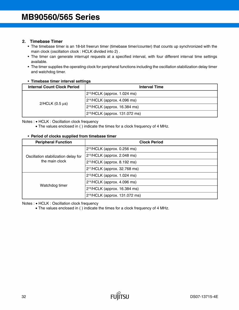
2. Timebase Timer• The timebase timer is an 18-bit freerun timer (timebase timer/counter) that counts up synchronized with the
main clock (oscillation clock : HCLK divided into 2) .• The timer can generate interrupt requests at a specified interval, with four different interval time settings
available.• The timer supplies the operating clock for peripheral functions including the oscillation stabilization delay timer
and watchdog timer.
• Timebase timer interval settings
Notes : • HCLK : Oscillation clock frequency • The values enclosed in ( ) indicate the times for a clock frequency of 4 MHz.
• Period of clocks supplied from timebase timer
Notes : • HCLK : Oscillation clock frequency • The values enclosed in ( ) indicate the times for a clock frequency of 4 MHz.
Internal Count Clock Period Interval Time
2/HCLK (0.5 µs)
212/HCLK (approx. 1.024 ms)
214/HCLK (approx. 4.096 ms)
216/HCLK (approx. 16.384 ms)
219/HCLK (approx. 131.072 ms)
Peripheral Function Clock Period
Oscillation stabilization delay for the main clock
210/HCLK (approx. 0.256 ms)
213/HCLK (approx. 2.048 ms)
215/HCLK (approx. 8.192 ms)
217/HCLK (approx. 32.768 ms)
Watchdog timer
212/HCLK (approx. 1.024 ms)
214/HCLK (approx. 4.096 ms)
216/HCLK (approx. 16.384 ms)
219/HCLK (approx. 131.072 ms)
32 DS07-13715-4E

MB90560/565 Series
• Block diagram
The actual interrupt request number for the timebase timer is : Interrupt request number : #36 (24H)
TBIE TBOF TBR TBC1 TBC0
× 21 × 22 × 23 × 28 × 29 × 210 × 211 × 212 × 213 × 214 × 215 × 216 × 217 × 218
OF OF OF OF
To PPG timer To watchdog timer
Timebase timer/counter
HCLKdivided into 2
To oscillation stabilizationdelay time selectorin clock controller
Reset*1
Clear stop mode, etc.*2
Switch clock mode*3
Counterclear circuit
TBOF clear TBOF set
Intervaltimer selector
Timebase timer control register (TBTC)
Timebase timer interrupt signal
OF : OverflowHCLK : Oscillation clock frequency
*1 : Power-on reset, watchdog reset*2 : Recovery from stop mode and timebase timer mode*3 : Main → PLL clock
DS07-13715-4E 33

MB90560/565 Series
3. Watchdog Timer• The watchdog timer is a timer/counter used to detect faults such as program runaway.• The watchdog timer is a 2-bit counter that counts the clock signal from the timebase timer or clock timer.• Once started, the watchdog timer must be cleared before the 2-bit counter overflows. If an overflow occurs,
the CPU is reset.
• Interval time for the watchdog timer
Notes : • The difference between the maximum and minimum watchdog timer interval times is due to the timing when the counter is cleared.• As the watchdog timer is a 2-bit counter that counts the carry-up signal from the timebase timer or clock timer, clearing the timebase timer (when operating on HCLK) or the clock timer (when operating on SCLK) lengthens the time until the watchdog timer reset is generated.
• Watchdog timer count clock
• Events that stop the watchdog timer
1 : Stop due to a power-on reset
2 : Watchdog reset
• Events that clear the watchdog timer
1 : External reset input from the RST pin.
2 : Writing “0” to the software reset bit.
3 : Writing “0” to the watchdog control bit (second and subsequent times) .
4 : Changing to sleep mode (clears the watchdog timer and temporarily halts the count) .
5 : Changing to timebase timer mode (clears the watchdog timer and temporarily halts the count) .
6 : Changing to stop mode (clears the watchdog timer and temporarily halts the count) .
HCLK : Oscillation Clock (4 MHz)
Min. Max. Clock Period
Approx. 3.58 ms Approx. 4.61 ms 214 ± 211 / HCLK
Approx. 14.33 ms Approx. 18.30 ms 216 ± 213 / HCLK
Approx. 57.23 ms Approx. 73.73 ms 218 ± 215 / HCLK
Approx. 458.75 ms Approx. 589.82 ms 218 ± 215 / HCLK
WTC : WDCS HCLK : Oscillation clockPCLK : PLL clock
“0” Prohibited setting
“1” Count the timebase timer output.
34 DS07-13715-4E

MB90560/565 Series
• Block diagram
PONR STBR WRST ERST SRST WTE WT1 WT0
× 21 × 22 × 28 × 29 × 210 × 211 × 212 × 213 × 214 × 215 × 216 × 217 × 218
2
4
Watchdog timer control register (WDTC)
Watchdog timer
ResetChange to sleep mode
Change to stop mode
Change to timebasetimer mode
Counter clearcontrol circuit
Counter clockselector
2-bit counter
Start
Clear
Watchdog timerreset generation
circuit
To internalreset circuit
Main clock (HCLK divided into 2)
(Timebase timer/counter)
HCLK : Oscillation clock frequency
DS07-13715-4E 35

MB90560/565 Series
4. 16-Bit Reload Timers 0 and 1 (With Event Count Function) • The 16-bit reload timers have the following functions.• The count clock can be selected from three internal clocks or the external event clock.• An interrupt to the CPU can be generated when an underflow occurs on 16-bit reload timer 0 or 1. This interrupt
allows the timers to be used as interval timers.• Two different operation modes can be selected when an underflow occurs on 16-bit reload timer 0 or 1: one-
shot mode in which timer operation halts when an underflow occurs or reload mode in which the value in thereload register is loaded into the timer and counting continues.
• Extended intelligent I/O service (EI2OS) is supported.• The MB90560/565 series contains two 16-bit reload timer channels.
• 16-bit reload timer operation modes
• Interval times for the 16-bit reload timers
Note : The values enclosed in ( ) and the example of interval times is for a machine clock frequency of 16 MHz. φ is the machine clock frequency value for the calculation.
Remarks : 16-bit reload timer 0 can be used to generate the baud rate for UART0. 16-bit reload timer 1 can be used to generate the baud rate for UART1 and activation trigger for the A/D converter.
Count Clock Start Trigger Operation When anUnderflow Occurs
Internal clock
Software triggerOne-shot mode
Reload mode
External triggerOne-shot mode
Reload mode
Event count mode (external clock mode)
Software triggerOne-shot mode
Reload mode
Count Clock Count Clock Period Example of Interval Times
Internal clock
21/φ (0.125 µs) 0.125 µs to 8.192 ms
23/φ (0.5 µs) 0.5 µs to 32.768 ms
25/φ (2.0 µs) 2.0 µs to 131.1 ms
Event count mode 23/φ or longer 0.5 µs or longer
36 DS07-13715-4E

MB90560/565 Series
• Block diagram
TMRLR0*1
TMRLR1*2
TMR0*1
TMR1*2
CLK
TIN0*1
TIN1*2
UF
EN TO0*1
TO1*2
CLK
3
3 2
⎯ ⎯ ⎯ ⎯ CSL1 CSL0 MOD2MOD1MOD0 OUTE OUTL RELD UFINTE CNTE TRG
*4
Internal data bus
16-bit reload register
Reload signal Reloadcontrol circuit
16-bit timer register
Count clock generation circuit
Machineclock φ Prescaler
Gate inputClockpulse
detectioncircuit
Cleartrigger
Internalclock
PinInput
controlcircuit
External clock
Clockselector
Selectsignal
Function selection
Timer control status register (TMCSR)
Wait signal
To UART0*1
To UART1 and A/D converter trigger*2
Output control circuit
Output signalgeneration circuit Pin
Operationcontrol circuit
Interruptrequest output#30 (1EH) *1, *3
#32 (20H) *2, *3
*1 : Channel 0*2 : Channel 1*3 : Interrupt number*4 : Underflow
DS07-13715-4E 37

MB90560/565 Series
5. Multi-Function Timer• Based on the 16-bit freerun timer, the multi-function timer can be used to generate 12 independent waveform
outputs and to measure input pulse widths and external clock periods.
• Structure of multi-function timer
• 16-bit freerun timer (1 channel)
The 16-bit freerun timer consists of a 16-bit up-counter (timer data register (TCDT) ) , compare clear register(CPCLR) , timer control status register (TCCS) , and prescaler.
The count output value from the 16-bit freerun timer provides the base time for the input capture and outputcompare functions.• The count clock can be selected from the following eight clocks :
1/φ, 2/φ, 4/φ, 8/φ, 16/φ, 32/φ, 64/φ, 128/φφ : Machine clock frequency
• An interrupt can be generated when the 16-bit freerun timer overflows or when the 16-bit freerun timer countis cleared to “0000H” due to a match occurring between the value in the compare clear register (CPCLR) andthe count in the 16-bit freerun timer (TCCS : ICRE = “1”, MODE = “1”) .
• The 16-bit freerun timer is cleared to “0000H” when a reset occurs, on setting the timer clear bit (SCLR) in thetimer control status register (TCCS) , when a compare match occurs between the 16-bit freerun timer countand the value in the compare clear register (CPCLR) (TCCS : MODE = “1”) , or by writing “0000H” to the timerdata register (TCDT) .
• Output compare (6 channels)
The output compare unit consists of compare registers (OCCP0 to OCCP5) , compare control registers (OCS0to OCS5) , and compare output latches.
When a match occurs between a compare register (OCCP0 to OCCP5) value and the count from the 16-bitfreerun timer, the output compare can invert the level of the corresponding output compare pin and generatean interrupt.• The compare registers (OCCP0 to OCCP5) operate independently for each channel. Each of the compare
registers (OCCP0 to OCCP5) has a corresponding output pin and an interrupt request flag in the channel’scompare control register (lower) (OCS0, OCS2, OCS4) .
• Two channels of the compare registers (OCCP0 to OCCP5) can be used to invert the output pins.• An interrupt can be output when a match occurs between a compare register (OCCP0 to OCCP5) and the
count from the 16-bit freerun timer (OCS0, OCS2, OCS4 : IOP0 = “1”, IOP1 = “1”) . (OCS0, OCS2, OCS4 :IOE0 = “1”, IOE1 = “1”)
• The initial output levels for the output compare pins can be set.
• Input capture (4 channels)
The input capture consists of external input pins (IN0 to IN3) , corresponding input capture data registers (IPCP0to IPCP3) , and input capture control status registers (ICS01, ICS23) .The input capture can transfer the count value from the 16-bit freerun timer to the input capture data register(IPCP0 to IPCP3) and output an interrupt on detecting an active edge on the signal input from the external inputpin.• Each channel of the input capture operates independently.• The active edge (rising edge, falling edge, or either edge) on the external signal can be specified.
16-bitfreerun timer
16-bitoutput compare
16-bitinput capture
8/16-bitPPG timer
Waveformgenerator
1 ch 6 ch 4 ch8 bit × 6 ch
16 bit × 3 ch8-bit timer × 3 ch
38 DS07-13715-4E
MB90560/565 Series
• An interrupt can be generated when an active edge is detected on the external signal (ICS01, ICS23 : ICE0= “1”, ICE1 = “1”, ICE2 = “1”, ICE3 = “1”) .
• 8/16-bit PPG timer (8-bit : 6 channels, 16-bit : 3 channels)
The 8/16-bit PPG timer consists of an 8-bit down counter (PCNT) , PPG control registers (PPGC0 to PPGC5) , PPG clock control registers (PCS01, PCS23, PCS45) , and PPG reload registers (PRLL0 to PRLL5, PRLH0to PRLH5) .When used as an 8/16-bit reload timer, the PPG operates as an event timer. The PPG can also be used to outputpulses with specified frequency and duty ratio.• 8-bit PPG mode
Each channel operates as an independent 8-bit PPG.• 8-bit prescaler + 8-bit PPG mode
ch0 (ch2, ch4) operates as an 8-bit prescaler and ch1 (ch3, ch5) operates as a variable frequency PPG bycounting up on the borrow output from ch0 (ch2, ch4) .
• 16-bit PPG modech0 (ch2, ch4) and ch1 (ch3, ch5) operate together as a 16-bit PPG.
• PPG operationOutputs pulses with the specified frequency and duty ratio (ratio of “H” level period and “L” level period), andcan also be used as a D/A converter when combined with an external circuit.
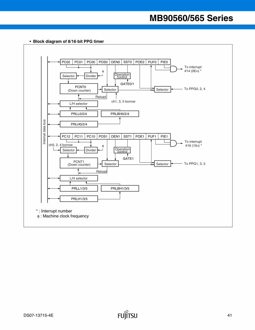
• Waveform generator
The waveform generator consists of an 8-bit timer, 8-bit timer control registers (DTCR0 to DTCR2) , 8-bit reloadregisters (TMRR0 to TMRR2) , and waveform control register (SIGCR) .
The waveform generator can generate a DC chopper output or non-overlapping three-phase waveform outputfor inverter control using the realtime outputs (RT0 to RT5) and 8/16-bit PPG timer.• A non-overlapping waveform can be generated by using the 8-bit timer as a deadtime timer and adding a non-
overlap time delay to the PPG timer pulse output. (Deadtime timer function) • A non-overlapping waveform can be generated by using the 8-bit timer as a deadtime timer and adding a non-
overlap time delay to the realtime outputs (RT1, RT3, RT5) . (Deadtime timer function) • A GATE signal can be generated when a match occurs between the count from the 16-bit freerun timer and
compare register in the output compare (OCCP0 to OCCP5) (rising edge on realtime output (RT) ) to controlthe PPG timer operation. (GATE function)
• Can control the RTO0 to RTO5 pin outputs using the DTTI pin input.By making the DTTI pin input clockless, the pins can be controlled externally even when the oscillation clockis halted. (The level for each pin can be set by the program.) However, the I/O ports (P30 to P35) must havebeen set beforehand as outputs and the output values set in the port 3 data register (PDR3) .
DS07-13715-4E 39

MB90560/565 Series
• Block diagram• 16-bit freerun timer, input capture, and output compare
φ
IVF8
IVFE STOP MODE SCLR CLK2 CLK1 CLK0
ICLR
IOP1 IOP0 IOE1 IOE0
ICP0 ICP1 ICE0 ICE1
EG11 EG10 EG01 EG00
IN0/2
IN1/3
CMOD
T Q
T Q
ICREMS13 to 0
3
16
16
16
4
4
4
Inte
rnal
dat
a bu
s
To interrupt#31 (1FH) *
Divider
Clock16-bit freerun timer
16-bit compare clear register Compare circuit
Compare registers 0, 2, 4
Compare circuit
Compare registers 1, 3, 5
Compare circuit
To interrupt#34 (22H) *
To A/D trigger
To RT0, 2, 4waveform generator
To RT1, 3, 5waveform generator
To interrupts
Capture registers 0, 2 Edge detection
Capture registers 1, 3 Edge detection
To interrupts
#13 (0DH) *, #17 (11H) *, #21 (15H) *
#15 (0FH) *, #19 (13H) *, #23 (17H) *
#33 (21H) *, #35 (23H) *
#33 (21H) *, #35 (23H) *
* : Interrupt numberφ : Machine clock frequency
40 DS07-13715-4E
MB90560/565 Series
• Block diagram of 8/16-bit PPG timer
φ
φ
PC02 PC01
PCNT0
PC00 POS0 OEN0 SST0 POE0 PUF0 PIE0
PC12 PC11 PC10 POS1 OEN1 SST1 POE1 PUF1 PIE1
GATE0/1
GATE1
PRLL0/2/4
PRLH0/2/4
PRLBH0/2/4
PRLL1/3/5
PRLH1/3/5
PRLBH1/3/5
Inte
rnal
dat
a bu
s
To interrupt#14 (0EH) *
Selector Divider Operationcontrol
Operationcontrol
(Down counter) Selector Selector To PPG0, 2, 4
Reloadch1, 3, 5 borrow
L/H selector
To interrupt #16 (10H) *ch0, 2, 4 borrow
Selector Divider
(Down counter) Selector Selector To PPG1, 3, 5
Reload
L/H selector
PCNT1
* : Interrupt numberφ : Machine clock frequency
DS07-13715-4E 41
MB90560/565 Series
• Block diagram of waveform generator
φDCK2 DCK1 DCK0 TMD1 TMD0 NRSL DTIL DTIE
DTTI
TO0
TO1
RTO0/U
RTO1/X
RTO2/V
RTO3/Y
RTO4/W
RTO5/Z
U
X
TO2
TO3
V
Y
TO4
TO5
W
RT4
RT5
RT2
RT3
RT0
RT1
Inte
rnal
dat
a bu
s
Divider
Clock
DTTI control circuit
To GATE0, 1 (To PPG timer)
Waveformgenerator
8-bit timer Compare circuit SelectorSelector
8-bit timer register 0 Deadtime generation
To GATE2, 3 (To PPG timer)
Waveformgenerator
Waveformgenerator
8-bit timer Compare circuit SelectorSelector
8-bit timer register 1 Deadtime generation
To GATE4, 5 (To PPG timer)
8-bit timer Compare circuit SelectorSelector
8-bit timer register 2 Deadtime generation
φ : Machine clock frequency
42 DS07-13715-4E
MB90560/565 Series
6. UART
(1) Overview• The UART is a general-purpose serial communications interface for performing synchronous or asynchronous
(start-stop synchronization) communications with external devices.• The interface provides both a bi-directional communication function (normal mode) and a master-slave com-
munication function (multi-processor mode) .• The UART can generate interrupt requests at receive complete, receive error detected, and transmit complete
timings. Also the UART supports EI2OS.
• UART functions
The UART is a general-purpose serial communications interface for sending serial data to and from other CPUsand peripheral devices.
Note : The UART does not add the start and stop bits in clock synchronous mode. In this case, only data is transmitted.
Function
Data buffer Full-duplex double-buffered
Transmission modes• Clock synchronous (no start and stop bits) • Clock asynchronous (start-stop synchronization)
Baud rate
• Max. 2 MHz (for a 16 MHz machine clock) • Baud rate generated by dedicated baud rate generator• Baud rate generated by external clock (clock input from SCK0 and SCK1 pins) • Baud rate generated by internal clock (clock supplied from 16-bit reload timer) • Eight different baud rate settings are available.
Number of data bits• 7 bits (asynchronous normal mode only) • 8 bits
Signal format Non return to zero (NRZ) format
Receive error detection• Framing errors• Overrun errors• Parity errors (not available in multi-processor mode)
Interrupt requests• Receive interrupt (Receive complete or receive error detected) • Transmit interrupt (Transmission complete) • Both transmit and receive support the extended intelligent I/O service (EI2OS) .
Master/slavecommunication function (multi-processor mode)
Used for 1 (master) to n (slave) communications. (Can only be used as master)
DS07-13715-4E 43

MB90560/565 Series
• UART operation modes
⎯ : Not available
*1 : The “+1” represents the address/data (A/D) bit used for communication control.
*2 : Only 1 stop bit supported for receiving.
• UART interrupts and EI2OS
: The UART has a function to halt EI2OS if a receive error is detected. : Available when the interrupt shared with ICR13 or ICR14 is not used.
Operation ModeNo. of Data Bits
Synchronization No. of Stop BitsNo Parity With Parity
0 Normal mode 7 or 8 bits Asynchronous1 or 2 bits*2
1 Multi-processor mode 8 + 1*1 ⎯ Asynchronous
2 Clock synchronous mode 8 ⎯ Synchronous None
Interrupt Interrupt No.
Interrupt ControlRegister Vector Table Address
EI2OSRegister
Name Address Lower Upper Bank
UART1receive interrupt
#37 (25H) ICR13 0000BDH FFFF68H FFFF69H FFFF6AH
UART1send interrupt
#38 (26H) ICR13 0000BDH FFFF64H FFFF65H FFFF66H
UART0receive interrupt
#39 (27H) ICR14 0000BEH FFFF60H FFFF61H FFFF62H
UART0send interrupt
#40 (28H) ICR14 0000BEH FFFF5CH FFFF5DH FFFF5EH
44 DS07-13715-4E

MB90560/565 Series
(2) UART structure
The UART consists of the following 11 blocks:
• Block diagram
• Clock selector • Mode registers (SMR0, SMR1) • Receive control circuit • Control registers (SCR0, SCR1) • Transmission control circuit • Status registers (SSR0, SSR1) • Receive status evaluation circuit • Input data registers (SIDR0, SIDR1) • Receive shift register • Output data registers (SODR0, SODR1) • Transmission shift register
MD1MD0CS2CS1CS0
SCKESOE
PENPSBLCLA/DRECRXETXE
PEOREFRERDRFTDREBDSRIETIE
SIDR0/SIDR1
P40/SCK0<P62/SCK1>
P37/SOT0<P61/SOT1>
#39 (27H)*<#37 (25H)*>
#40 (28H)*<#38 (26H)*>
P36/SIN0<P60/SIN1>
SODR0/SODR1
Control bus
Dedicated baudrate generator
16-bit reload timer
Pin
Clockselector Receive
clock Receivecontrol circuit
Start bitdetection circuit
Transmissionstart circuit
Transmit bitcounter
Receive paritycounter
Transmit paritycounter
Receiveshift register
Receive bitcounter
Pin
Receivecomplete
Receive statusevaluation circuit
Internal data bus
Transmit clock
Receiveinterrupt signal
Transmitinterrupt signal
Transmissioncontrol circuit
Pin
Transmissionshift register
Transmission start
Receive error detectionsignal for EI2OS (to CPU)
SMR0/SMR1 SCR0/SCR1 SSR0/SSR1
* : Interrupt number
DS07-13715-4E 45

MB90560/565 Series
• Clock selector
Selects the send/receive clock from either the dedicated baud rate generator, external input clock (clock inputto SCK0 or SCK1 pin) , or internal clock (clock supplied by 16-bit reload timer) .
• Receive control circuit
The receive control circuit consists of a receive bit counter, start bit detection circuit, and receive parity counter.The receive bit counter counts the received data bits and outputs a receive interrupt request when the requirednumber of data bits have been received. The start bit detection circuit detects the start bit on the serial inputsignal. On detecting a start bit, the receive data is shifted to the input data register (SIDR0 or SIDR1) inaccordance with the specified transfer speed. The receive parity counter calculates the parity of the receiveddata if parity is selected.
• Transmission control circuit
The transmission control circuit consists of a transmission bit counter, transmission start circuit, and transmissionparity counter. The transmission bit counter counts the transmitted data bits and outputs a transmit interruptrequest when the required number of data bits have been sent. The transmission start circuit starts transmissionwhen data is written to the output data register (SODR0 or SODR1) . The transmission parity counter generatesthe parity bit for the transmitted data when parity is selected.
• Receive shift register
The receive shift register captures the data input from the SIN0 or SIN1 pin by shifting one bit at a time thentransfers the received data to the input data register (SIDR0 or SIDR1) when reception completes.
• Transmission shift register
The transmission data is transferred from the output data register (SODR0 or SODR1) to the transmission shiftregister and output from the SOT0 or SOT1 pin by shifting one bit at a time.
• Mode register (SMR0, SMR1)
Set the operation mode, baud rate clock and serial clock input/output control, and enables output for the serial data pin.
• Control register (SCR0, SCR1)
Specifies whether to use parity, the type of parity, number of stop bits and data bits and the frame data formatfor operation mode 1, to clear the receive error flag bit, and to enable or disable send and receive operation.
• Status register (SSR0, SSR1)
Stores the send/receive and error status information, set the serial data transfer direction, and enables or disablesthe send and receive interrupt requests.
• Input data register (SIDR0, SIDR1)
Stores the received data.
• Output data register (SODR0, SODR1)
Set the transmission data. The data set in the output data register is converted to serial format and output.
46 DS07-13715-4E
MB90560/565 Series
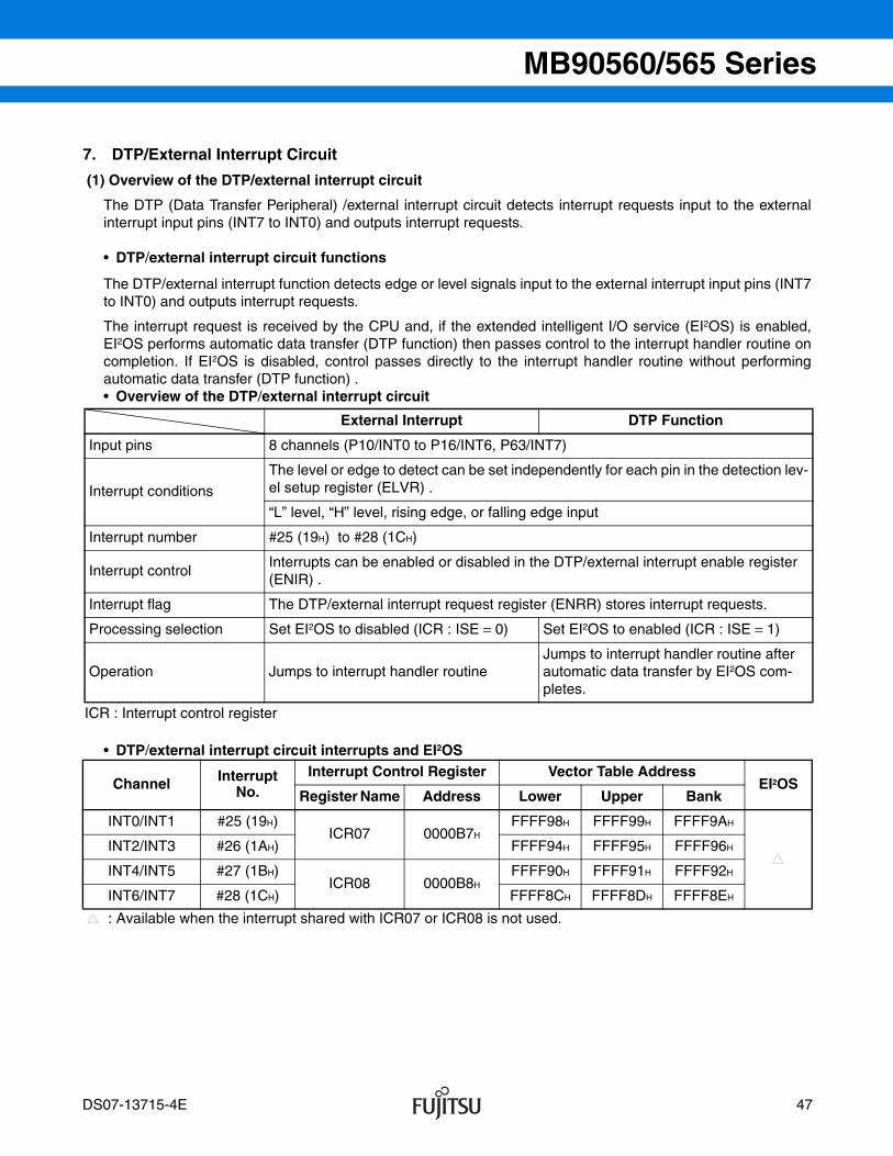
7. DTP/External Interrupt Circuit
(1) Overview of the DTP/external interrupt circuit
The DTP (Data Transfer Peripheral) /external interrupt circuit detects interrupt requests input to the externalinterrupt input pins (INT7 to INT0) and outputs interrupt requests.
• DTP/external interrupt circuit functions
The DTP/external interrupt function detects edge or level signals input to the external interrupt input pins (INT7to INT0) and outputs interrupt requests.
The interrupt request is received by the CPU and, if the extended intelligent I/O service (EI2OS) is enabled,EI2OS performs automatic data transfer (DTP function) then passes control to the interrupt handler routine oncompletion. If EI2OS is disabled, control passes directly to the interrupt handler routine without performingautomatic data transfer (DTP function) .• Overview of the DTP/external interrupt circuit
• DTP/external interrupt circuit interrupts and EI2OS
: Available when the interrupt shared with ICR07 or ICR08 is not used.
Channel Interrupt No.
Interrupt Control Register Vector Table AddressEI2OS
Register Name Address Lower Upper Bank
INT0/INT1 #25 (19H) ICR07 0000B7H
FFFF98H FFFF99H FFFF9AH
INT2/INT3 #26 (1AH) FFFF94H FFFF95H FFFF96H
INT4/INT5 #27 (1BH) ICR08 0000B8H
FFFF90H FFFF91H FFFF92H
INT6/INT7 #28 (1CH) FFFF8CH FFFF8DH FFFF8EH
ICR : Interrupt control register
External Interrupt DTP Function
Input pins 8 channels (P10/INT0 to P16/INT6, P63/INT7)
Interrupt conditions
The level or edge to detect can be set independently for each pin in the detection lev-el setup register (ELVR) .
“L” level, “H” level, rising edge, or falling edge input
Interrupt number #25 (19H) to #28 (1CH)
Interrupt controlInterrupts can be enabled or disabled in the DTP/external interrupt enable register (ENIR) .
Interrupt flag The DTP/external interrupt request register (ENRR) stores interrupt requests.
Processing selection Set EI2OS to disabled (ICR : ISE = 0) Set EI2OS to enabled (ICR : ISE = 1)
Operation Jumps to interrupt handler routineJumps to interrupt handler routine after automatic data transfer by EI2OS com-pletes.
DS07-13715-4E 47

MB90560/565 Series
(2) Structure of the DTP/external interrupt circuit
The DTP/external interrupt circuit consists of the following four blocks : • DTP/interrupt detection circuit• DTP/interrupt request register (EIRR) • DTP/interrupt enable register (ENIR) • Request level setting register (ELVR)
• Block diagram
LB7
ER7 ER6 ER5 ER4 ER3 ER2 ER1 ER0
EN7 EN6 EN5 EN4 EN3 EN2 EN1 EN0
P63/INT7 P10/INT0
LA7 LB6 LA6 LB5 LA5 LB4 LA4 LB3 LA3 LB2 LA2 LB1 LA1 LB0 LA0
P16/INT6 P11/INT1
P12/INT2
P13/INT3
P15/INT5
P14/INT4
#25 (19H)*
#26 (1AH)*
#27 (1BH)*
#28 (1CH)*
2 2 2 2 2 2 2 2
Inte
rnal
dat
a bu
s
Request level setting register (ELVR)
Pin
Pin
Pin
Pin
Selector
Selector
Selector Selector
Selector
Selector
Selector Selector
Pin
Pin
Pin
Pin
DTP/external interrupt input detection circuit
DTP/interruptrequest register (EIRR)
DTP/interruptenable register (ENIR)
Interrupt request signal
* : Interrupt number
48 DS07-13715-4E

MB90560/565 Series
8. Delayed Interrupt Generation Module• The delayed interrupt generation module is used to generate the task switching interrupt. Generation of this
hardware interrupt can be specified by software.
• Delayed interrupt generation module functions
• Block diagram
Function and Control
Interrupt trigger
• Writing “1” to bit R0 of the delayed interrupt request generation/clear register(DIRR : R0 = 1) generates an interrupt request.
• Writing “0” to bit R0 of the delayed interrupt request generation/clear register(DIRR : R0 = 1) clears the interrupt request.
Interrupt control • No enable/disable register is provided for this interrupt.
Interrupt flag• Set in bit R0 of the delayed interrupt request generation/clear register
(DIRR : R0) .
EI2OS support • Not supported by the extended intelligent I/O service (EI2OS) .
⎯ ⎯ ⎯ ⎯ ⎯ ⎯ ⎯ R0
Internal data bus
Delayed interrupt request generation/clear register (DIRR)
S
R
Interruptrequest signal
Interrupt requestlatch
⎯ : Undefined
DS07-13715-4E 49
MB90560/565 Series
9. 8/10-Bit A/D Converter• Overview of the 8/10-bit A/D converter• The 8/10-bit A/D converter uses RC successive approximation to convert analog input voltages to an 8-bit or
10-bit digital value.• The input signals can be selected from the eight analog input pin channels.
• 8/10-bit A/D converter functions
• 8/10-bit A/D converter conversion modes
• 8/10-bit A/D converter interrupts and EI2OS
: Available
A/D conversion timeThe minimum conversion time is 6.13 µs (for a 16 MHz machine clock, including sampling time) .The minimum sampling time is 2.0 µs (for a 16 MHz machine clock)
Conversion method RC successive approximation with sample & hold circuit
Resolution 8-bit or 10-bit, selectable
Analog input pins Eight analog input pin channels are available. The input pin can be selected by the program.
InterruptsAn interrupt request can be generated and EI2OS invoked when A/D conversion completes.The conversion data protection function operates when A/D conversion is performed with the interrupt enabled.
A/D conversionstart trigger
The conversion start trigger can be set from the following options : software, output of 16-bit reload timer 1 (rising edge) , or zero detection edge from 16-bit freerun timer.
EI2OS support Supported by the extended intelligent I/O service (EI2OS) .
Conversion Mode Single Conversion Mode Operation Scan Conversion Mode Operation
Single-shot conversion mode 1Single-shot conversion mode 2
Performs one conversion for the spec-ified channel (1 channel) then halts.
Sequentially performs one conversion for multiple channels (up to 8 channels can be set) , then halts.
Continuous conversion modePerforms repeated conversions for the specified channel (1 channel) .
Performs repeated conversions for the specified channels (up to 8 channels can be set) .
Incremental conversion modePerforms one conversion for the spec-ified channel (1 channel) then halts and waits for the next activation.
Sequentially performs one conversion for multiple channels (up to 8 channels can be set) , then halts and waits for the next activation.
Interrupt No.Interrupt Control Register Vector Table Address
EI2OSRegister Name Address Lower Upper Bank
#11 (0BH) ICR00 0000B0H FFFFD0H FFFFD1H FFFFD2H
50 DS07-13715-4E
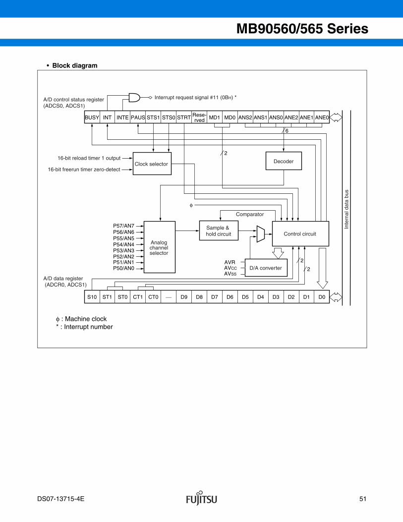
MB90560/565 Series
• Block diagram
BUSY INT INTE PAUS STS1 STS0 STRT Rese-rved MD1 MD0 ANS2 ANS1 ANS0 ANE2 ANE1 ANE0
S10 ST1 ST0 CT1 CT0 D9 D7 D6 D4 D3 D2 D1 D0
P57/AN7P56/AN6P55/AN5P54/AN4P53/AN3P52/AN2P51/AN1P50/AN0
AVRAVCC
AVSS
D8 D5
φ
⎯
2
2
6
2
A/D control status register(ADCS0, ADCS1)
A/D data register (ADCR0, ADCS1)
Interrupt request signal #11 (0BH) *
16-bit reload timer 1 output
16-bit freerun timer zero-detectClock selector Decoder
Inte
rnal
dat
a bu
s
Analogchannelselector
Sample & hold circuit
Comparator
Control circuit
D/A converter
φ : Machine clock* : Interrupt number
DS07-13715-4E 51

MB90560/565 Series
10. ROM Mirror Function Selection Module• The ROM mirror function selection module enables ROM data in FF bank to be read by accessing 00 bank.
• ROM mirror function selection module functions
• Relationship between addresses in the ROM mirror function
• Block diagram
Function
Mirror setting address• Data in FFFFFFH to FF4000H in FF bank can be read from 00FFFFH to 004000H
in 00 bank.
Interrupts • None
EI2OS support • Not supported by the extended intelligent I/O service (EI2OS) .
FE0000H
FE8000H
FF8000H
FF0000H
FF4000H
FEFFFFH
FFFFFFH
FF bank
Mirrored ROMdata area
ROM area in MB90568 and MB90F568
ROM area in MB90567
ROM area in MB90562/A and MB90F562/B
ROM area in MB90561/A
⎯ ⎯ ⎯ ⎯ ⎯ ⎯ ⎯ MI
ROM
ROM mirror function selection register (ROMM)
Inte
rnal
dat
a bu
s
FF bank
Address
Data
00 bank
Address space
52 DS07-13715-4E
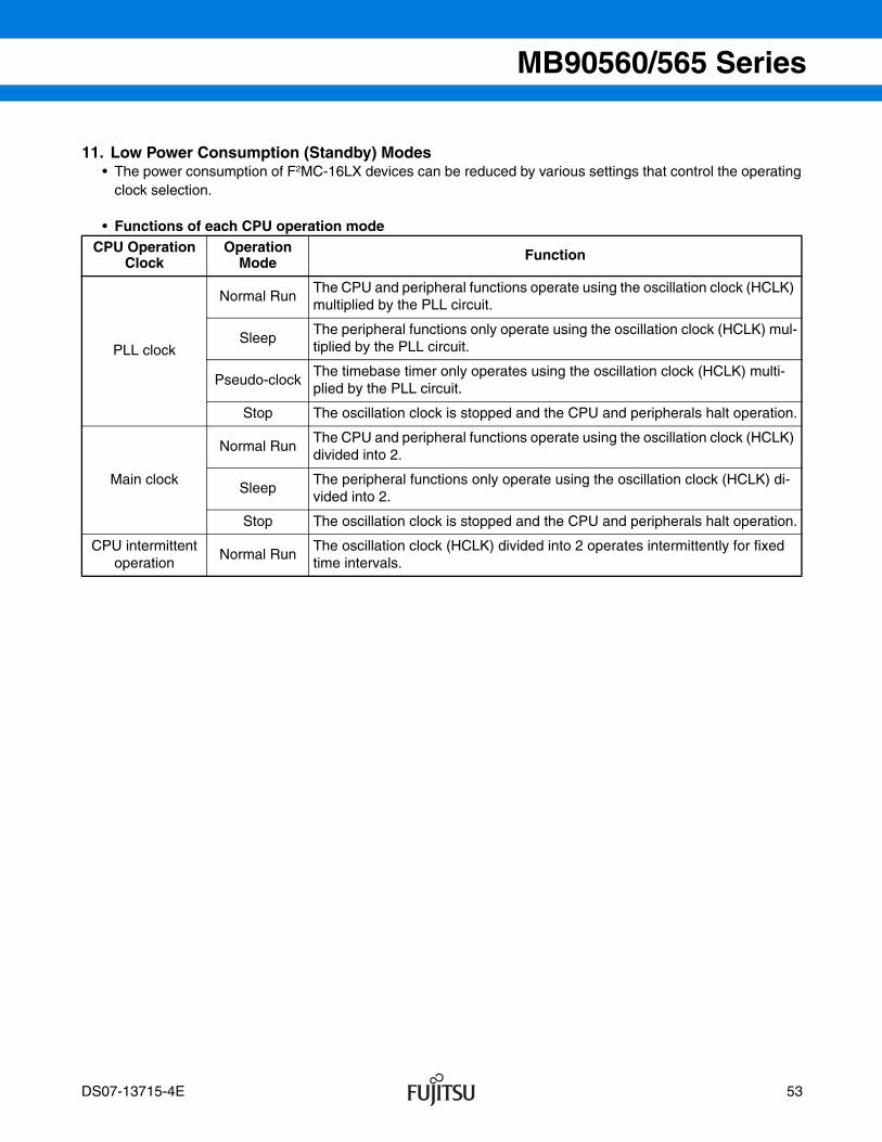
MB90560/565 Series
11. Low Power Consumption (Standby) Modes• The power consumption of F2MC-16LX devices can be reduced by various settings that control the operating
clock selection.
• Functions of each CPU operation modeCPU Operation
ClockOperation
Mode Function
PLL clock
Normal RunThe CPU and peripheral functions operate using the oscillation clock (HCLK) multiplied by the PLL circuit.
SleepThe peripheral functions only operate using the oscillation clock (HCLK) mul-tiplied by the PLL circuit.
Pseudo-clockThe timebase timer only operates using the oscillation clock (HCLK) multi-plied by the PLL circuit.
Stop The oscillation clock is stopped and the CPU and peripherals halt operation.
Main clock
Normal RunThe CPU and peripheral functions operate using the oscillation clock (HCLK) divided into 2.
SleepThe peripheral functions only operate using the oscillation clock (HCLK) di-vided into 2.
Stop The oscillation clock is stopped and the CPU and peripherals halt operation.
CPU intermittent operation
Normal RunThe oscillation clock (HCLK) divided into 2 operates intermittently for fixed time intervals.
DS07-13715-4E 53
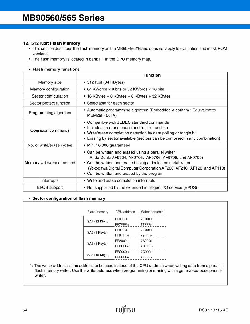
MB90560/565 Series
12. 512 Kbit Flash Memory• This section describes the flash memory on the MB90F562/B and does not apply to evaluation and mask ROM
versions.• The flash memory is located in bank FF in the CPU memory map.
• Flash memory functions
• Sector configuration of flash memory
Function
Memory size • 512 Kbit (64 KBytes)
Memory configuration • 64 KWords × 8 bits or 32 KWords × 16 bits
Sector configuration • 16 KBytes + 8 KBytes + 8 KBytes + 32 KBytes
Sector protect function • Selectable for each sector
Programming algorithm• Automatic programming algorithm (Embedded Algorithm : Equivalent to
MBM29F400TA)
Operation commands
• Compatible with JEDEC standard commands• Includes an erase pause and restart function• Write/erase completion detection by data polling or toggle bit• Erasing by sector available (sectors can be combined in any combination)
No. of write/erase cycles • Min. 10,000 guaranteed
Memory write/erase method
• Can be written and erased using a parallel writer (Ando Denki AF9704, AF9705, AF9706, AF9708, and AF9709)
• Can be written and erased using a dedicated serial writer (Yokogawa Digital Computer Corporation AF200, AF210, AF120, and AF110)
• Can be written and erased by the program
Interrupts • Write and erase completion interrupts
EI2OS support • Not supported by the extended intelligent I/O service (EI2OS) .
SA1 (32 Kbyte)
SA2 (8 Kbyte)
SA3 (8 Kbyte)
SA4 (16 Kbyte)
FF0000H
FF7FFFH
FF8000H
FF9FFFH
FFA000H
FFBFFFH
FFC000H
FEFFFFH
70000H
77FFFH
78000H
79FFFH
7A000H
7BFFFH
7C000H
7FFFFH
Flash memory CPU address Writer address*
* : The writer address is the address to be used instead of the CPU address when writing data from a parallel flash memory writer. Use the writer address when programming or erasing with a general-purpose parallel writer.
54 DS07-13715-4E

MB90560/565 Series
13. 1 Mbit Flash Memory• This section describes the flash memory on the MB90F568 and does not apply to evaluation and mask ROM
versions.• The flash memory is located in banks FE to FF in the CPU memory map.
• Flash memory functions
• Sector configuration of flash memory
Function
Memory size • 1 Mbit (128 KBytes)
Memory configuration • 128 KWords × 8 bits or 64 KWords × 16 bits
Sector configuration • 16 KBytes + 8 KBytes + 8 KBytes + 32 KBytes + 64 KBytes
Sector protect function • Selectable for each sector
Programming algorithm• Automatic programming algorithm (Embedded Algorithm : Equivalent to
MBM29F400TA)
Operation commands
• Compatible with JEDEC standard commands• Includes an erase pause and restart function• Write/erase completion detection by data polling or toggle bit• Erasing by sector available (sectors can be combined in any combination)
No. of write/erase cycles • Min. 10,000 guaranteed
Memory write/erase method
• Can be written and erased using a parallel writer (Ando Denki AF9704, AF9705, AF9706, AF9708, and AF9709)
• Can be written and erased using a dedicated serial writer (Yokogawa Digital Computer Corporation AF200, AF210, AF120, and AF110)
• Can be written and erased by the program
Interrupts • Write and erase completion interrupts
EI2OS support • Not supported by the extended intelligent I/O service (EI2OS) .
SA0 (64 Kbyte)
SA1 (32 Kbyte)
SA2 (8 Kbyte)
SA3 (8 Kbyte)
SA4 (16 Kbyte)
FE0000H
FEFFFH
FF0000H
FF7FFFH
FF8000H
FF9FFFH
FFA000H
FFBFFFH
FFC000H
FEFFFFH
60000H
6FFFFH
70000H
77FFFH
78000H
79FFFH
7A000H
7BFFFH
7C000H
7FFFFH
Flash memory CPU address Writer address*
* : The writer address is the address to be used instead of the CPU address when writing data from a parallel flash memory writer. Use the writer address when programming or erasing with a general-purpose parallel writer.
DS07-13715-4E 55
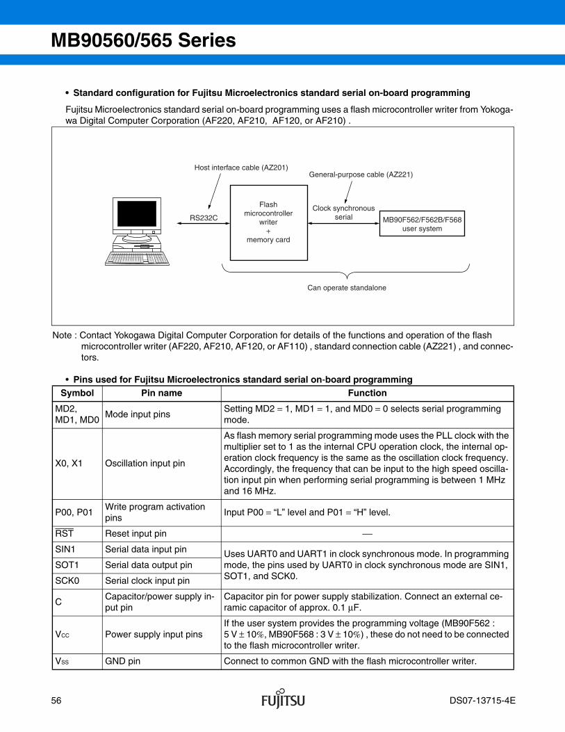
MB90560/565 Series
• Standard configuration for Fujitsu Microelectronics standard serial on-board programming
Fujitsu Microelectronics standard serial on-board programming uses a flash microcontroller writer from Yokoga-wa Digital Computer Corporation (AF220, AF210, AF120, or AF210) .
Note : Contact Yokogawa Digital Computer Corporation for details of the functions and operation of the flash microcontroller writer (AF220, AF210, AF120, or AF110) , standard connection cable (AZ221) , and connec-tors.
• Pins used for Fujitsu Microelectronics standard serial on-board programmingSymbol Pin name Function
MD2, MD1, MD0
Mode input pinsSetting MD2 = 1, MD1 = 1, and MD0 = 0 selects serial programming mode.
X0, X1 Oscillation input pin
As flash memory serial programming mode uses the PLL clock with the multiplier set to 1 as the internal CPU operation clock, the internal op-eration clock frequency is the same as the oscillation clock frequency. Accordingly, the frequency that can be input to the high speed oscilla-tion input pin when performing serial programming is between 1 MHz and 16 MHz.
P00, P01Write program activation pins
Input P00 = “L” level and P01 = “H” level.
RST Reset input pin ⎯
SIN1 Serial data input pin Uses UART0 and UART1 in clock synchronous mode. In programming mode, the pins used by UART0 in clock synchronous mode are SIN1, SOT1, and SCK0.
SOT1 Serial data output pin
SCK0 Serial clock input pin
CCapacitor/power supply in-put pin
Capacitor pin for power supply stabilization. Connect an external ce-ramic capacitor of approx. 0.1 µF.
VCC Power supply input pinsIf the user system provides the programming voltage (MB90F562 : 5 V ± 10%, MB90F568 : 3 V ± 10%) , these do not need to be connected to the flash microcontroller writer.
VSS GND pin Connect to common GND with the flash microcontroller writer.
Host interface cable (AZ201)General-purpose cable (AZ221)
Flashmicrocontroller
writer +
memory card
Clock synchronousserial MB90F562/F562B/F568
user system
Can operate standalone
RS232C
56 DS07-13715-4E
asatani
ノート
asatani : Marked
asatani
ノート
asatani : Marked
asatani
ノート
asatani : Marked
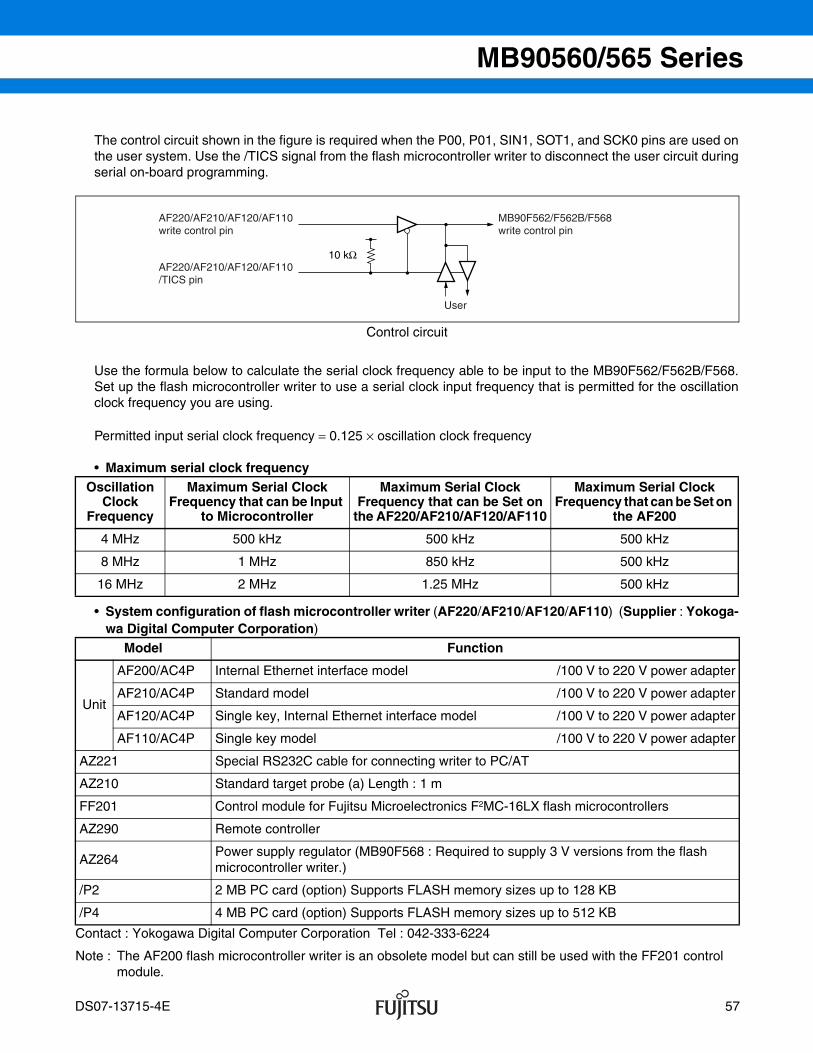
MB90560/565 Series
The control circuit shown in the figure is required when the P00, P01, SIN1, SOT1, and SCK0 pins are used onthe user system. Use the /TICS signal from the flash microcontroller writer to disconnect the user circuit duringserial on-board programming.
Control circuit
Use the formula below to calculate the serial clock frequency able to be input to the MB90F562/F562B/F568.Set up the flash microcontroller writer to use a serial clock input frequency that is permitted for the oscillationclock frequency you are using.
Permitted input serial clock frequency = 0.125 × oscillation clock frequency
• Maximum serial clock frequency
• System configuration of flash microcontroller writer (AF220/AF210/AF120/AF110) (Supplier : Yokoga-wa Digital Computer Corporation)
Contact : Yokogawa Digital Computer Corporation Tel : 042-333-6224
Note : The AF200 flash microcontroller writer is an obsolete model but can still be used with the FF201 control module.
Oscillation Clock
Frequency
Maximum Serial Clock Frequency that can be Input
to Microcontroller
Maximum Serial Clock Frequency that can be Set on
the AF220/AF210/AF120/AF110
Maximum Serial Clock Frequency that can be Set on
the AF200
4 MHz 500 kHz 500 kHz 500 kHz
8 MHz 1 MHz 850 kHz 500 kHz
16 MHz 2 MHz 1.25 MHz 500 kHz
Model Function
Unit
AF200/AC4P Internal Ethernet interface model /100 V to 220 V power adapter
AF210/AC4P Standard model /100 V to 220 V power adapter
AF120/AC4P Single key, Internal Ethernet interface model /100 V to 220 V power adapter
AF110/AC4P Single key model /100 V to 220 V power adapter
AZ221 Special RS232C cable for connecting writer to PC/AT
AZ210 Standard target probe (a) Length : 1 m
FF201 Control module for Fujitsu Microelectronics F2MC-16LX flash microcontrollers
AZ290 Remote controller
AZ264Power supply regulator (MB90F568 : Required to supply 3 V versions from the flash microcontroller writer.)
/P2 2 MB PC card (option) Supports FLASH memory sizes up to 128 KB
/P4 4 MB PC card (option) Supports FLASH memory sizes up to 512 KB
10 kΩ
AF220/AF210/AF120/AF110write control pin
AF220/AF210/AF120/AF110/TICS pin
MB90F562/F562B/F568write control pin
User
DS07-13715-4E 57
asatani
ノート
asatani : Marked
MB90560/565 Series
ELECTRICAL CHARACTERISTICS (MB90560 SERIES) 1. Absolute Maximum Ratings
(VSS = AVSS = 0.0 V)
*1 : AVCC and AVR must not exceed VCC. Also, AVR must not exceed AVCC.
*2 : VI and VO must not exceed VCC + 0.3 V.
*3 : The maximum output current is the peak value for a single pin.
*4 : Pins other than P30/RTO0 to P35/RTO5
*5 : P30/RTO0 to P35/RTO5 pins
WARNING: Semiconductor devices can be permanently damaged by application of stress (voltage, current, temperature, etc.) in excess of absolute maximum ratings. Do not exceed these ratings.
Parameter SymbolRating
Unit RemarksMin. Max.
Power supply voltage
VCC VSS − 0.3 VSS + 6.0 V
AVCC VSS − 0.3 VSS + 6.0 V VCC ≥ AVCC*1
AVR VSS − 0.3 VSS + 6.0 V AVCC ≥ AVR ≥ 0 V *1
Input voltage VI VSS − 0.3 VSS + 6.0 V *2
Output voltage VO VSS − 0.3 VSS + 6.0 V *2
“L” level maximum output current
IOL1 ⎯ 15 mA *3, *4
IOL2 ⎯ 20 mA *3, *5
“L” level average output current
IOLAV1 ⎯ 4 mAAverage value (operating current × operating ratio) *4
IOLAV2 ⎯ 12 mAAverage value (operating current × operating ratio) *5
“L” level total maximum output current
ΣIOL ⎯ 100 mA
“L” level total average output current
ΣIOLAV ⎯ 50 mAAverage value (operating current × operating ratio)
“H” level maximum output current
IOH ⎯ −15 mA *3
“H” level average output current
IOHAV ⎯ −4 mAAverage value (operating current × operating ratio)
“H” level total maximum output current
ΣIOH ⎯ −100 mA
“H” level total average output current
ΣIOHAV ⎯ −50 mAAverage value (operating current × operating ratio)
Power consumption Pd ⎯ 300 mW
Operating temperature TA −40 +85 °C
Storage temperature Tstg −55 +150 °C
58 DS07-13715-4E

MB90560/565 Series
2. Recommended Operating Conditions (VSS = AVSS = 0.0 V)
WARNING: The recommended operating conditions are required in order to ensure the normal operation of the semiconductor device. All of the device's electrical characteristics are warranted when the device is operated within these ranges.
Always use semiconductor devices within their recommended operating condition ranges. Operation outside these ranges may adversely affect reliability and could result in device failure.No warranty is made with respect to uses, operating conditions, or combinations not represented on the data sheet. Users considering application outside the listed conditions are advised to contact their representatives beforehand.
Parameter SymbolValue
Unit RemarksMin. Max.
Power supply voltageVCC
3.0 5.5 VNormal operation (MB90562, 562A, 561, 561A, and V560)
4.5 5.5 V Normal operation (MB90F562 and F562B)
VCC 3.0 5.5 V Maintaining state in stop mode
Input “H” voltage
VIH 0.7 VCC VCC + 0.3 V CMOS input pin
VIHS 0.8 VCC VCC + 0.3 V CMOS hysteresis input pin
VIHM VCC − 0.3 VCC + 0.3 V MD input pin
Input “L” voltage
VIL VSS − 0.3 0.3 VCC V CMOS input pin
VILS VSS − 0.3 0.2 VCC V CMOS hysteresis input pin
VILM VSS − 0.3 VSS + 0.3 V MD input pin
Smoothing capacitor CS 0.1 1.0 µF
Use a ceramic capacitor or other capacitor with equivalent frequency characteristics.The capacitance of the smoothing capacitor connected to the VCC pin must be greater than CS.
Operating temperature
TA −40 +85 °C
C
CS
• C pin diagram
DS07-13715-4E 59

MB90560/565 Series
3. DC Characteristics (TA = −40 °C to +85 °C, VCC = 5.0 V ±10%, VSS = AVSS = 0.0 V)
* : Value when low power mode bits (LPM0, 1) is set to “01” with an internal operating frequency of 4 MHz.
Note : Current values are provisional and are subject to change without notice to allow for improvements to the characteristics. The power supply current is measured with an external clock.
Parameter Sym-bol Pin Name Condition
ValueUnit Remarks
Min. Typ. Max.
Output “H” voltage
VOHAll output pins
VCC = 4.5 VIOH = −2.0 mA
VCC − 0.5 ⎯ ⎯ V
Output “L” voltage
VOL1
Pins other than P30/RTO0 to P35/RTO5
VCC = 4.5 VIOL1 = 2.0 mA
⎯ ⎯ 0.4 V
VOL2
P30/RTO0 to P35/RTO5
VCC = 4.5 VIOL2 = 12.0 mA
⎯ ⎯ 0.8 V
Input leak current
IILAll output pins
VCC = 5.5 VVSS < VI < VCC
−5 ⎯ 5 µA
Power supply current*
ICC
VCC
For VCC = 5 V, internal frequency = 16 MHz, normal operation
⎯ 50 80 mAMB90562/A, MB90561/A
⎯ 40 50 mA MB90F562/B
For VCC = 5 V, internal frequency = 16 MHz, A/D operation in progress
⎯ 55 85 mAMB90562/A, MB90561/A
⎯ 45 55 mA MB90F562/B
Flash write or erase ⎯ 45 60 mA MB90F562/B
ICCS
For VCC = 5 V, internal frequency = 16 MHz, sleep mode
⎯ 15 20 mAMB90562/A, MB90561/A, MB90F562/B*
ICCH Stop mode, TA = 25 °C ⎯ 5 20 µA
Input capacitance
CIN
Other than AVCC, AVSS, C, VCC, and VSS
⎯ ⎯ 10 80 pF
Pull-up resistor
RUP
P00 to P07P10 to P17RST
⎯ 15 30 100 kΩ
Pull-down resistor
RDOWN MD2 ⎯ 15 30 100 kΩ Only for mask ROM products
60 DS07-13715-4E
asatani
ノート
asatani : Marked
Added the “Only mask ROM product” in the remarks column of Pull-down resistor.
Deleted the pin name MD0, MD1 of Pull-up resistor.

MB90560/565 Series
4. AC Characteristics
(1) Clock Timings (TA = −40 °C to +85 °C, VCC = 5.0 V ±10%, VSS = AVSS = 0.0 V)
Parameter Symbol Pin Name Condi-
tionValue
Unit RemarksMin. Typ. Max.
Clock frequency fC X0, X1
⎯
3 ⎯ 16MHz
With a PLL circuit
1 ⎯ 16 Without a PLL circuit
Clock cycle time tHCYL X0, X162.5 ⎯ 333
nsWith a PLL circuit
62.5 ⎯ 1000 Without a PLL circuit
Input clock pulse widthPWH
PWLX0 10 ⎯ ⎯ ns
Recommended duty ratio = 30% to 70%
Input clock rise/fall timetcrtcf
X0 ⎯ ⎯ 5 nsWhen using an external clock
Internal operating clock frequency
fCP ⎯ 1.5 ⎯ 16 MHzWhen using a main clock
Internal operating clock cycle time
tCP ⎯ 62.5 ⎯ 333 nsWhen using a main clock
0.8 VCC
0.2 VCC
tcf tcr
tHCYL
PWH PWL
X0
• X0 and X1 clock timing
DS07-13715-4E 61

MB90560/565 Series
The AC ratings are specified for the following measurement reference voltages.
• PLL guaranteed operation rangeRelationship between internal operating clock frequency and power supply voltage
Relationship between oscillation frequency and internal operating clock frequency
5.5
4.5
3.33.0
1 3 8 12 16
Guaranteed operation rangefor MB90F562/B
PLL guaranteed operation range
PLL guaranteedoperation range
A/D converter guaranteedoperation range
Guaranteed operation rangefor MB90561/A and MB90562/A
Guaranteed operation range for MB90V560
Sup
ply
Vol
tage
VC
C (
V)
Internal Clock fCP (MHz)
16
12
8
432
1 2 3 4 6 8 12 16
×4 ×3 ×2 ×1
No multiplier
Inte
rnal
Clo
ck fC
P (
MH
z)
Source Oscillation Clock fC (MHz)
0.5
0.8 VCC
0.2 VCC
2.4 V
0.8 V
0.7 VCC
0.3 VCC
• Input signal waveform
Hysteresis input pin
Pins other than hysteresis input or MD input pins
• Output signal waveform
Output pin
62 DS07-13715-4E
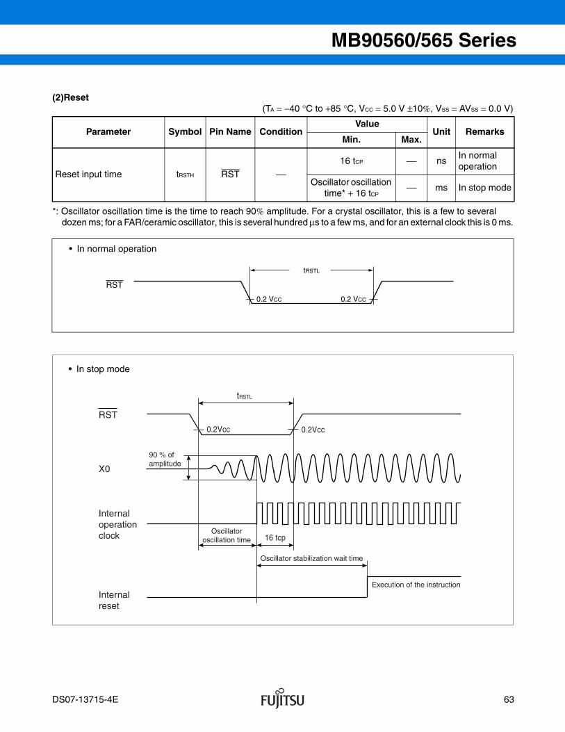
MB90560/565 Series
(2)Reset (TA = −40 °C to +85 °C, VCC = 5.0 V ±10%, VSS = AVSS = 0.0 V)
*: Oscillator oscillation time is the time to reach 90% amplitude. For a crystal oscillator, this is a few to several dozen ms; for a FAR/ceramic oscillator, this is several hundred µs to a few ms, and for an external clock this is 0 ms.
Parameter Symbol Pin Name ConditionValue
Unit RemarksMin. Max.
Reset input time tRSTH RST ⎯16 tCP ⎯ ns
In normal operation
Oscillator oscillation time* + 16 tCP
⎯ ms In stop mode
RST
0.2 VCC
tRSTL
0.2 VCC
• In normal operation
RST
X0
16 tcp
tRSTL
0.2Vcc 0.2Vcc
Internaloperationclock
Internalreset
90 % ofamplitude
Oscillatoroscillation time
Oscillator stabilization wait time
Execution of the instruction
• In stop mode
DS07-13715-4E 63

MB90560/565 Series
(3) Power-On Reset (TA = −40 °C to +85 °C, VCC = 5.0 V ±10%, VSS = AVSS = 0.0 V)
Note: VCC must be less than 0.2 V before power-on.
Notes : • The above rating values are for generating a power-on reset. • Some internal registers are only initialized by a power-on reset. Always apply the power supply in accordance with the above ratings if you wish to initialize these registers.
Parameter Symbol Pin Name Condi-tion
ValueUnit Remarks
Min. Max.
Power supply rise time tR VCC⎯
0.05 30 ms
Power supply cutoff time tOFF VCC 4 ⎯ ms For repeated operation
VCC
VCC
3.0 V
VSS
tR
0.2 V0.2 V
2.7 V
tOFF
0.2 V
Maintain RAM data
Recommended rate of voltage rise is 50 mV/ms or less.
Sudden changes in the power supply voltage may cause a power-on reset.The recommended practice if you wish to change the power supply voltage while the device is operating is to raise the voltage smoothly as shown below. Also, changes to the supply voltage should be performed when the PLL clock is not in use. The PLL clock may be used, however, if the rate of voltage change is 1 V/s or less.
64 DS07-13715-4E
asatani
ノート
asatani : Marked
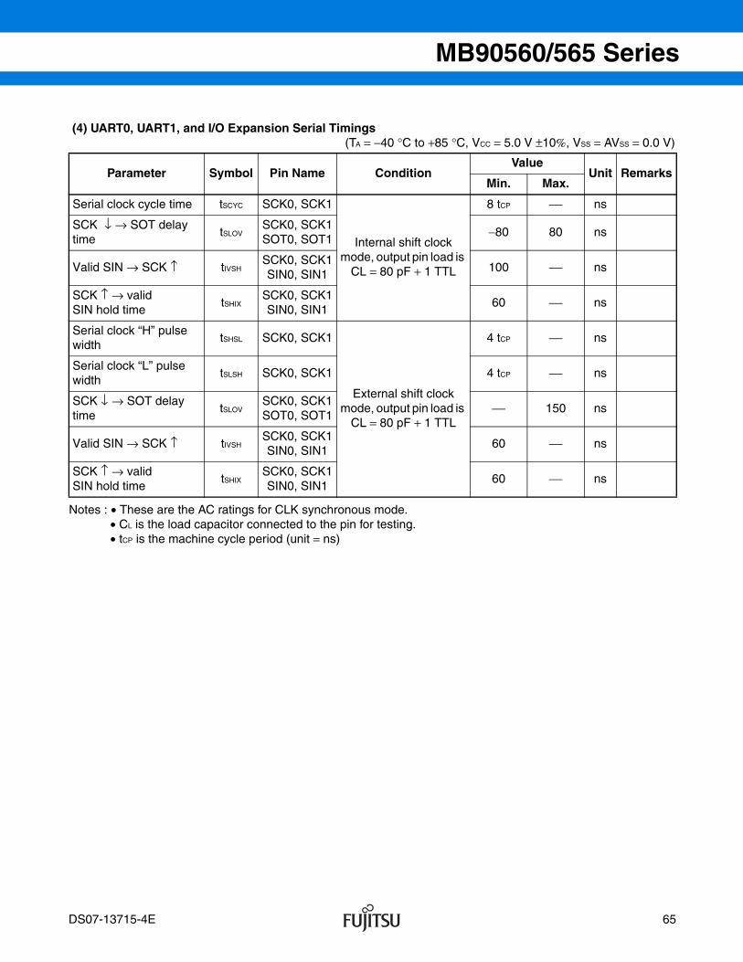
MB90560/565 Series
(4) UART0, UART1, and I/O Expansion Serial Timings (TA = −40 °C to +85 °C, VCC = 5.0 V ±10%, VSS = AVSS = 0.0 V)
Notes : • These are the AC ratings for CLK synchronous mode. • CL is the load capacitor connected to the pin for testing. • tCP is the machine cycle period (unit = ns)
Parameter Symbol Pin Name ConditionValue
Unit RemarksMin. Max.
Serial clock cycle time tSCYC SCK0, SCK1
Internal shift clock mode, output pin load is
CL = 80 pF + 1 TTL
8 tCP ⎯ ns
SCK ↓ → SOT delay time
tSLOVSCK0, SCK1SOT0, SOT1
−80 80 ns
Valid SIN → SCK ↑ tIVSHSCK0, SCK1SIN0, SIN1
100 ⎯ ns
SCK ↑ → validSIN hold time
tSHIXSCK0, SCK1SIN0, SIN1
60 ⎯ ns
Serial clock “H” pulse width
tSHSL SCK0, SCK1
External shift clock mode, output pin load is
CL = 80 pF + 1 TTL
4 tCP ⎯ ns
Serial clock “L” pulse width
tSLSH SCK0, SCK1 4 tCP ⎯ ns
SCK ↓ → SOT delay time
tSLOVSCK0, SCK1SOT0, SOT1
⎯ 150 ns
Valid SIN → SCK ↑ tIVSHSCK0, SCK1SIN0, SIN1
60 ⎯ ns
SCK ↑ → validSIN hold time
tSHIXSCK0, SCK1SIN0, SIN1
60 ⎯ ns
DS07-13715-4E 65
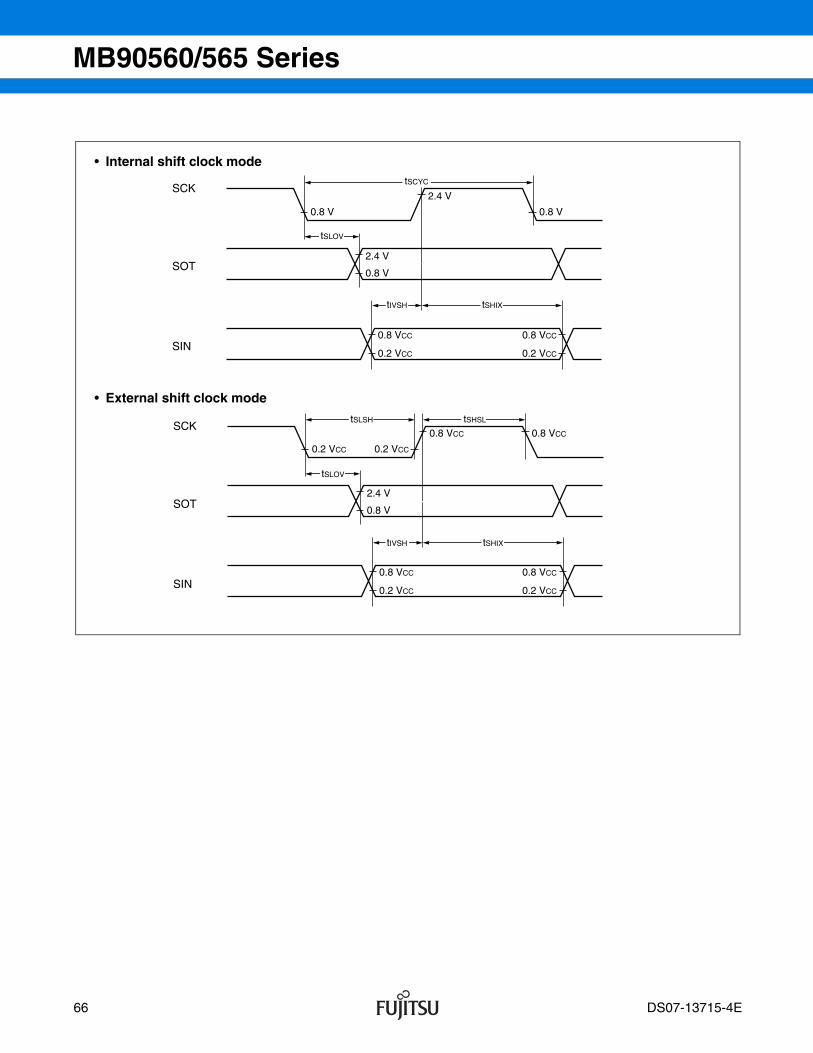
MB90560/565 Series
• Internal shift clock mode
• External shift clock mode
SCK
SOT
SIN
tSCYC
tSLOV
tIVSH tSHIX
0.8 V 0.8 V
2.4 V
2.4 V
0.8 V
0.8 VCC
0.2 VCC
0.8 VCC
0.2 VCC
SCK
SOT
SIN
tSLSH tSHSL
tSLOV
tIVSH tSHIX
0.2 VCC 0.2 VCC
0.8 VCC 0.8 VCC
2.4 V
0.8 V
0.8 VCC
0.2 VCC
0.8 VCC
0.2 VCC
66 DS07-13715-4E
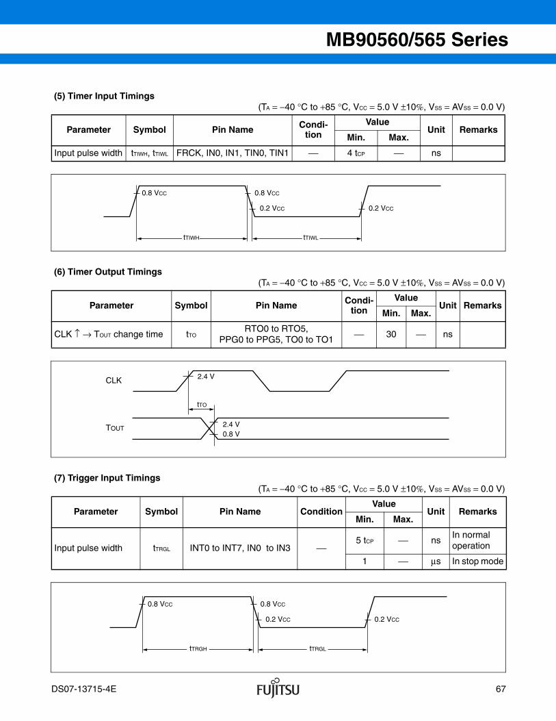
MB90560/565 Series
(5) Timer Input Timings (TA = −40 °C to +85 °C, VCC = 5.0 V ±10%, VSS = AVSS = 0.0 V)
(6) Timer Output Timings (TA = −40 °C to +85 °C, VCC = 5.0 V ±10%, VSS = AVSS = 0.0 V)
(7) Trigger Input Timings (TA = −40 °C to +85 °C, VCC = 5.0 V ±10%, VSS = AVSS = 0.0 V)
Parameter Symbol Pin Name Condi-tion
ValueUnit Remarks
Min. Max.
Input pulse width tTIWH, tTIWL FRCK, IN0, IN1, TIN0, TIN1 ⎯ 4 tCP ⎯ ns
Parameter Symbol Pin Name Condi-tion
ValueUnit Remarks
Min. Max.
CLK ↑ → TOUT change time tTORTO0 to RTO5,
PPG0 to PPG5, TO0 to TO1⎯ 30 ⎯ ns
Parameter Symbol Pin Name ConditionValue
Unit RemarksMin. Max.
Input pulse width tTRGL INT0 to INT7, IN0 to IN3 ⎯5 tCP ⎯ ns
In normaloperation
1 ⎯ µs In stop mode
0.8 VCC 0.8 VCC
0.2 VCC 0.2 VCC
tTIWH tTIWL
CLK
TOUT
2.4 V
tTO
2.4 V0.8 V
0.8 VCC 0.8 VCC
0.2 VCC 0.2 VCC
tTRGH tTRGL
DS07-13715-4E 67

MB90560/565 Series
5. Electrical Characteristics for the A/D Converter (TA = −40 °C to +85 °C, 3.0 V ≤ AVR, VCC = AVCC = 5.0 V ±10%, VSS = AVSS = 0.0 V)
* : Current when A/D converter is not used and CPU is in stop mode (VCC = AVCC = AVR = 5.0 V)
Notes : • The L reference voltage is fixed to AVSS. The relative error increases as AVR becomes smaller. • Ensure that the output impedance of the external circuit connected to the analog input meets the following
condition : Output impedance of external circuit ≤ 10 kΩ (Sampling Time = 4.0 µs)
• If the output impedance of the external circuit is too high, the analog voltage sampling time may be too short.
Parameter Symbol Pin NameValue
Unit RemarksMin. Typ. Max.
Resolution ⎯ ⎯ ⎯ 10 ⎯ bit
Total error ⎯ ⎯ ⎯ ⎯ ±5.0 LSB
Non-linearity error ⎯ ⎯ ⎯ ⎯ ±2.5 LSB
Differential linearity error ⎯ ⎯ ⎯ ⎯ ±1.9 LSB
Zero transition voltage VOT AN0 to AN7AVSS
−3.5 LSB+0.5
AVSS
+4.5 LSBmV
1 LSB = AVRH/1024Full-scale transition voltage
VFST AN0 to AN7AVR
−6.5 LSBAVR
−1.5 LSBAVR
+1.5 LSBmV
Conversion time ⎯ ⎯ ⎯ 176 tCP ⎯ ns
Sampling time ⎯ ⎯ ⎯ 64 tCP ⎯ ns
Analog port input current
IAIN AN0 to AN7 ⎯ ⎯ 10 µA
Analog input voltage VAIN AN0 to AN7 0 ⎯ AVR V
Reference voltage ⎯ AVR 2.7 ⎯ AVCC V
Power supply currentIA AVCC ⎯ 5 ⎯ mA
IAH AVCC ⎯ ⎯ 5 µA *
Reference voltage supply current
IR AVR ⎯ 400 ⎯ µA
IRH AVR ⎯ ⎯ 5 µA *
Variation between channels
⎯ AN0 to AN7 ⎯ ⎯ 4 LSB
• Equivalent circuit of analog input circuitCRON
Analog input
Comparator
MB90561/A, MB90562/A RON = 2.2 kΩ approx. C = 45 pF approx.
MB90F562 RON = 3.2 kΩ approx. C = 30 pF approx.
MB90F562/B RON = 2.6 kΩ approx. C = 28 pF approx.
Note : The values listed are an indication only.
68 DS07-13715-4E

MB90560/565 Series
6. Flash Memory Erase and Programming Performance
Parameter ConditionValue
Units RemarksMin Typ Max
Sector erase time
TA = + 25 °CVcc = 5.0 V
⎯ 1 15 sExcludes 00H programming prior erasure
Chip erase time ⎯ 5 ⎯ sExcludes 00H programming prior erasure
Word (16 bit width) programming time
⎯ 16 3,600 µs Excludes system-level overhead
Erase/Program cycle ⎯ 10,000 ⎯ ⎯ cycle
Data holding time ⎯ 100,000 ⎯ ⎯ h
DS07-13715-4E 69

MB90560/565 Series
ELECTRICAL CHARACTERISTICS (MB90565 SERIES) 1. Absolute Maximum Ratings
(VSS = AVSS = 0.0 V)
*1 : AVCC and AVR must not exceed VCC. Also, AVR must not exceed AVCC.
*2 : VI and VO must not exceed VCC + 0.3 V.
*3 : The maximum output current is the peak value for a single pin.
WARNING: Semiconductor devices can be permanently damaged by application of stress (voltage, current, temperature, etc.) in excess of absolute maximum ratings. Do not exceed these ratings.
Parameter SymbolRating
Unit RemarksMin. Max.
Power supply voltage
VCC VSS − 0.3 VSS + 4.0 V
AVCC VSS − 0.3 VSS + 4.0 V VCC ≥ AVCC*1
AVR VSS − 0.3 VSS + 4.0 V AVCC ≥ AVR ≥ 0 V *1
Input voltage VI VSS − 0.3 VSS + 4.0 V *2
Output voltage VO VSS − 0.3 VSS + 4.0 V *2
“L” level maximum output current
IOL ⎯ 15 mA *3
“L” level average output current
IOLAV ⎯ 4 mAAverage value (operating current × operating ratio)
“L” level total maximum output current
ΣIOL ⎯ 100 mA
“L” level total average output current
ΣIOLAV ⎯ 50 mAAverage value (operating current × operating ratio)
“H” level maximum output current
IOH ⎯ −15 mA *3
“H” level average output current
IOHAV ⎯ −4 mAAverage value (operating current × operating ratio)
“H” level total maximum output current
ΣIOH ⎯ −100 mA
“H” level total average output current
ΣIOHAV ⎯ −50 mAAverage value (operating current × operating ratio)
Power consumption Pd ⎯ 300 mW
Operating temperature TA −40 +85 °C
Storage temperature Tstg −55 +150 °C
70 DS07-13715-4E

MB90560/565 Series
2. Recommended Operating Conditions (VSS = AVSS = 0.0 V)
WARNING: The recommended operating conditions are required in order to ensure the normal operation of the semiconductor device. All of the device's electrical characteristics are warranted when the device is operated within these ranges.
Always use semiconductor devices within their recommended operating condition ranges. Operation outside these ranges may adversely affect reliability and could result in device failure.No warranty is made with respect to uses, operating conditions, or combinations not represented on the data sheet. Users considering application outside the listed conditions are advised to contact their representatives beforehand.
Parameter SymbolValue
Unit RemarksMin. Max.
Power supply voltage VCC
3.0 3.6 V Normal operation (MB90V560)
2.7 3.6 VNormal operation (MB90F568, MB90567 and MB90568)
2.5 3.6 V Maintaining state in stop mode
Input “H” voltage
VIH 0.7 VCC VCC + 0.3 V CMOS input pin
VIHS 0.8 VCC VCC + 0.3 V CMOS hysteresis input pin
VIHM VCC − 0.3 VCC + 0.3 V MD input pin
Input “L” voltage
VIL VSS − 0.3 0.3 VCC V CMOS input pin
VILS VSS − 0.3 0.2 VCC V CMOS hysteresis input pin
VILM VSS − 0.3 VSS + 0.3 V MD input pin
Operating temperature TA −40 +85 °C
DS07-13715-4E 71

MB90560/565 Series
3. DC Characteristics (TA = −40 °C to +85 °C, VCC = 2.7 V to 3.6 V, VSS = AVSS = 0.0 V)
* : Value when low power mode bits (LPM0, 1) are set to “01” with an internal operating frequency of 8 MHz.(Continued)
Parameter Symbol Pin Name Condition
ValueUnit Remarks
Min. Typ. Max.
Output “H” voltage
VOHAll output pins
VCC = 3.0 VIOH = −2.0 mA
VCC − 0.5 VCC − 0.3 ⎯ V
Output “L” voltage
VOLAll output pins
VCC = 3.0 VIOL = 2.0 mA
⎯ 0.2 0.4 V
Input leak current
IILAll output pins
VCC = 3.0 VVSS < VI < VCC
−5 −1 5 µA
Power supply current*
ICC
VCC
For VCC = 3.3 V, internal frequency = 8 MHz, normal operation
⎯ 14 22 mA MB90567/568
For VCC = 3.3 V, internal frequency = 16 MHz, normal operation
⎯ 27 40 mA MB90567/568
For VCC = 3.3 V, internal frequency = 8 MHz, A/D operation in progress
⎯ 18 27 mA MB90567/568
For VCC = 3.3 V, internal frequency = 16 MHz, A/D operation in progress
⎯ 32 45 mA MB90567/568
For VCC = 3.3 V, internal frequency = 8 MHz, normal operation
⎯ 18 28 mA MB90F568
For VCC = 3.3 V, internal frequency = 16 MHz, normal operation
⎯ 36 45 mA MB90F568
For VCC = 3.3 V, internal frequency = 8 MHz, A/D operation in progress
⎯ 23 33 mA MB90F568
For VCC = 3.3 V, internal frequency = 16 MHz, A/D operation in progress
⎯ 41 50 mA MB90F568
Flash write or erase ⎯ 40 50 mA MB90F568
ICCS
For VCC = 3.3 V, internal frequency = 8 MHz, sleep mode
⎯ 6 10 mAMB90567/568MB90F568*
For VCC = 3.3 V, internal frequency = 16 MHz, sleep mode
⎯ 14 20 mAMB90567/568MB90F568*
ICCH Stop mode, TA = 25 °C ⎯ 5 20 µA
72 DS07-13715-4E

MB90560/565 Series
(Continued)
Note : Current values are provisional and are subject to change without notice to allow for improvements to the characteristics. The power supply current is measured with an external clock.
Parameter Sym-bol Pin Name Condition
ValueUnit Remarks
Min. Typ. Max.
Pull-up resistor
RUP
P00 to P07P10 to P17RST
⎯ 20 65 200 kΩ
Pull-down resistor
RDOWN MD2 ⎯ 20 65 200 kΩOnly for mask ROM products
DS07-13715-4E 73
Added the “Only mask ROM product” in the remarks column of Pull-down resistor.
Deleted the pin name MD0, MD1 of Pull-up resistor.
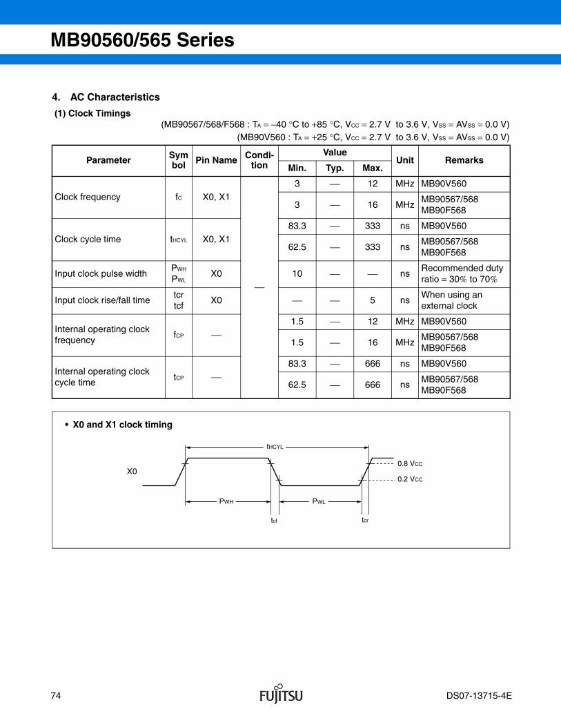
MB90560/565 Series
4. AC Characteristics
(1) Clock Timings (MB90567/568/F568 : TA = −40 °C to +85 °C, VCC = 2.7 V to 3.6 V, VSS = AVSS = 0.0 V)
(MB90V560 : TA = +25 °C, VCC = 2.7 V to 3.6 V, VSS = AVSS = 0.0 V)
Parameter Symbol Pin Name Condi-
tionValue
Unit RemarksMin. Typ. Max.
Clock frequency fC X0, X1
⎯
3 ⎯ 12 MHz MB90V560
3 ⎯ 16 MHzMB90567/568MB90F568
Clock cycle time tHCYL X0, X1
83.3 ⎯ 333 ns MB90V560
62.5 ⎯ 333 nsMB90567/568MB90F568
Input clock pulse widthPWH
PWLX0 10 ⎯ ⎯ ns
Recommended duty ratio = 30% to 70%
Input clock rise/fall timetcrtcf
X0 ⎯ ⎯ 5 nsWhen using an external clock
Internal operating clock frequency
fCP ⎯1.5 ⎯ 12 MHz MB90V560
1.5 ⎯ 16 MHzMB90567/568MB90F568
Internal operating clock cycle time
tCP ⎯83.3 ⎯ 666 ns MB90V560
62.5 ⎯ 666 nsMB90567/568MB90F568
0.8 VCC
0.2 VCC
tcf tcr
tHCYL
PWH PWL
X0
• X0 and X1 clock timing
74 DS07-13715-4E
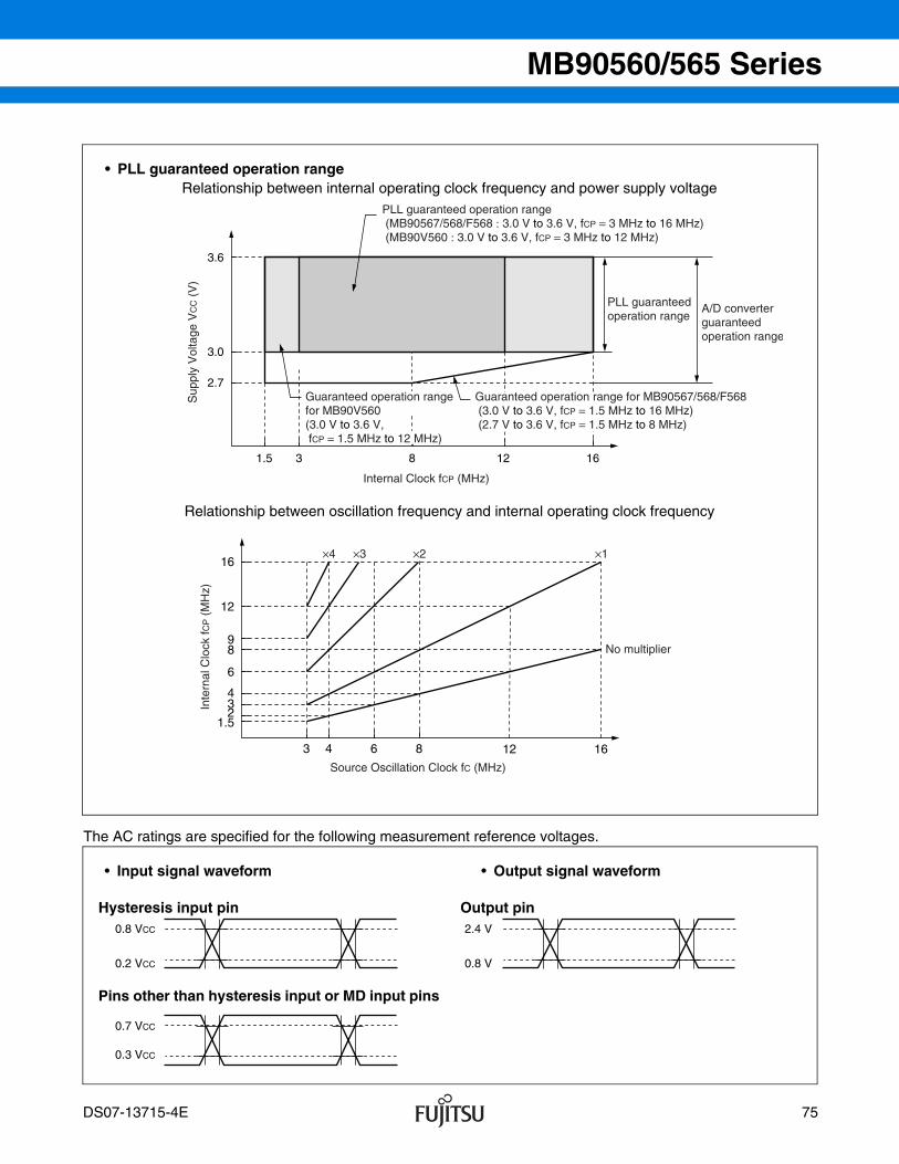
MB90560/565 Series
The AC ratings are specified for the following measurement reference voltages.
• PLL guaranteed operation rangeRelationship between internal operating clock frequency and power supply voltage
Relationship between oscillation frequency and internal operating clock frequency
3.6
3.0
2.7
1.5 3 8 12 16
PLL guaranteed operation range (MB90567/568/F568 : 3.0 V to 3.6 V, fCP = 3 MHz to 16 MHz) (MB90V560 : 3.0 V to 3.6 V, fCP = 3 MHz to 12 MHz)
PLL guaranteedoperation range
A/D converterguaranteedoperation range
Guaranteed operation range for MB90567/568/F568 (3.0 V to 3.6 V, fCP = 1.5 MHz to 16 MHz) (2.7 V to 3.6 V, fCP = 1.5 MHz to 8 MHz)
Sup
ply
Vol
tage
VC
C (
V)
Internal Clock fCP (MHz)
Guaranteed operation rangefor MB90V560(3.0 V to 3.6 V, fCP = 1.5 MHz to 12 MHz)
16
12
8
6
9
43
1.52
3 4 6 8 12 16
×4 ×3 ×2 ×1
No multiplier
Inte
rnal
Clo
ck fC
P (
MH
z)
Source Oscillation Clock fC (MHz)
0.8 VCC
0.2 VCC
2.4 V
0.8 V
0.7 VCC
0.3 VCC
• Input signal waveform
Hysteresis input pin
Pins other than hysteresis input or MD input pins
• Output signal waveform
Output pin
DS07-13715-4E 75
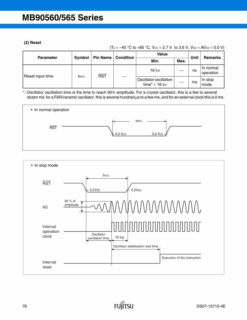
MB90560/565 Series
(2) Reset (TA = −40 °C to +85 °C, VCC = 2.7 V to 3.6 V, VSS = AVSS = 0.0 V)
*: Oscillator oscillation time is the time to reach 90% amplitude. For a crystal oscillator, this is a few to several dozen ms; for a FAR/ceramic oscillator, this is several hundred µs to a few ms, and for an external clock this is 0 ms.
Parameter Symbol Pin Name ConditionValue
Unit RemarksMin. Max.
Reset input time tRSTL RST ⎯16 tCP ⎯ ns
In normal operation
Oscillator oscillation time* + 16 tCP
⎯ msIn stop mode
RST
0.2 VCC
tRSTL
0.2 VCC
• In normal operation
RST
X0
16 tcp
tRSTL
0.2Vcc 0.2Vcc
Internaloperationclock
Internalreset
90 % ofamplitude
Oscillatoroscillation time
Oscillator stabilization wait time
Execution of the instruction
• In stop mode
76 DS07-13715-4E

MB90560/565 Series
(3) Power-On Reset (TA = −40 °C to +85 °C, VCC = 2.7 V to 3.6 V, VSS = AVSS = 0.0 V)
* : VCC must be less than 0.2 V before power-on.
Notes : • The above rating values are for generating a power-on reset. • Some internal registers are only initialized by a power-on reset. Always apply the power supply in
accordance with the above ratings if you wish to initialize these registers.
Parameter Symbol Pin Name Condi-tion
ValueUnit Remarks
Min. Max.
Power supply rise time tR VCC*
⎯0.05 30 ms
Power supply cutoff time tOFF VCC 4 ⎯ ms For repeated operation
VCC
VCC
2.5 V
VSS
tR
0.2 V0.2 V
2.7 V
tOFF
0.2 V
Maintain RAM data
Recommended rate of voltagerise is 50 mV/ms or less.
Sudden changes in the power supply voltage may cause a power-on reset.The recommended practice if you wish to change the power supply voltage while the device is operating is to raise the voltage smoothly as shown below. Also, changes to the supply voltage should be performed when the PLL clock is not in use. The PLL clock may be used, however, if the rate of voltage change is 1 V/s or less.
DS07-13715-4E 77

MB90560/565 Series
(4) UART0 and UART1 (TA = −40 °C to +85 °C, VCC = 2.7 V to 3.6 V, VSS = AVSS = 0.0 V)
Notes : • These are the AC ratings for CLK synchronous mode. • CV is the load capacitor connected to the pin for testing. • tCP is the machine cycle period (unit = ns)
Parameter Symbol Pin Name ConditionValue
Unit RemarksMin. Max.
Serial clock cycle time tSCYC SCK0, SCK1
Internal shift clock mode, output pin
load is CL = 80 pF + 1 TTL
8 tCP ⎯ ns
SCK ↓ → SOT delay time tSLOVSCK0, SCK1SOT0, SOT1
−80 80 ns
Valid SIN → SCK ↑ tIVSHSCK0, SCK1SIN0, SIN1
100 ⎯ ns
SCK ↑ → valid SIN hold time tSHIXSCK0, SCK1SIN0, SIN1
60 ⎯ ns
Serial clock “H” pulse width tSHSL SCK0, SCK1
External shift clock mode, output pin
load is CL = 80 pF + 1 TTL
4 tCP ⎯ ns
Serial clock “L” pulse width tSLSH SCK0, SCK1 4 tCP ⎯ ns
SCK ↓ → SOT delay time tSLOVSCK0, SCK1SOT0, SOT1
⎯ 150 ns
Valid SIN → SCK ↑ tIVSHSCK0, SCK1SIN0, SIN1
60 ⎯ ns
SCK ↑ → valid SIN hold time tSHIXSCK0, SCK1SIN0, SIN1
60 ⎯ ns
78 DS07-13715-4E

MB90560/565 Series
• Internal shift clock mode
• External shift clock mode
SCK
SOT
SIN
tSCYC
tSLOV
tIVSH tSHIX
0.8 V 0.8 V
2.4 V
2.4 V
0.8 V
0.8 VCC
0.2 VCC
0.8 VCC
0.2 VCC
SCK
SOT
SIN
tSLSH tSHSL
tSLOV
tIVSH tSHIX
0.2 VCC 0.2 VCC
0.8 VCC 0.8 VCC
2.4 V
0.8 V
0.8 VCC
0.2 VCC
0.8 VCC
0.2 VCC
DS07-13715-4E 79

MB90560/565 Series
(5) Timer Input Timings (TA = −40 °C to +85 °C, VCC = 2.7 V to 3.6 V, VSS = AVSS = 0.0 V)
(6) Timer Output Timings (TA = −40 °C to +85 °C, VCC = 2.7 V to 3.6 V, VSS = AVSS = 0.0 V)
(7) Trigger Input Timings (TA = −40 °C to +85 °C, VCC = 2.7 V to 3.6 V, VSS = AVSS = 0.0 V)
Parameter Symbol Pin Name Condi-tion
ValueUnit Remarks
Min. Max.
Input pulse width tTIWH, tTIWL FRCK, TIN0, TIN1 ⎯ 4 tCP ⎯ ns
Parameter Symbol Pin Name ConditionValue
Unit RemarksMin. Max.
CLK ↑ → TOUT change time
tTORTO0 to RTO5, PPG0 to PPG5
TO0, TO1⎯ 30 ⎯ ns
Parameter Symbol Pin Name ConditionValue
Unit RemarksMin. Max.
Input pulse width tTRGL INT0 to INT7, IN0 to IN3 ⎯5 tCP ⎯ ns
In normaloperation
1 ⎯ µs In stop mode
0.8 VCC
FRCKTIN0 to 1
0.8 VCC
0.2 VCC 0.2 VCC
tTIWH tTIWL
CLK
TOUT
2.4 V
tTO
2.4 V0.8 V
0.8 VCC
INT0 to INT7IN0 to IN3
0.8 VCC
0.2 VCC 0.2 VCC
tTRGH tTRGL
80 DS07-13715-4E

MB90560/565 Series
5. Electrical Characteristics for the A/D Converter (MB90567/568/F568 : TA = −40 °C to +85 °C, 2.7 V ≤ AVR, VCC = AVCC = 2.7 V to 3.6 V, VSS = AVSS = 0.0 V)
(MB90V560 : TA = +25 °C, 3.0 V ≤ AVR, VCC = AVCC = 3.0 V to 3.6 V, VSS = AVSS = 0.0 V)
* : Current when A/D converter is not used and CPU is in stop mode (VCC = AVCC = AVR = 3.3 V)
Notes : • The L reference voltage is fixed to AVSS. The relative error increases as AVR becomes smaller. • Ensure that the output impedance of the external circuit connected to the analog input meets the following
condition : Output impedance of MB90F568 external circuit ≤ 14 kΩ (Sampling Time = 4 µs) Output impedance of MB90567/568 external circuit ≤ 7 kΩ (Sampling Time = 4 µs) • If the output impedance of the external circuit is too high, the analog voltage sampling time may be too short.
Parameter Symbol Pin NameValue
Unit RemarksMin. Typ. Max.
Resolution ⎯ ⎯ ⎯ ⎯ 10 bit
Total error ⎯ ⎯ ⎯ ⎯ ±3.0 LSB
Non-linearity error ⎯ ⎯ ⎯ ⎯ ±2.5 LSB
Differential linearity error
⎯ ⎯ ⎯ ⎯ ±1.9 LSB
Zero transition voltage
VOT AN0 to AN7AVSS
−1.5 LSBAVSS
+0.5AVSS
+2.5 LSBmV
1 LSB = AVRH/1024Full-scale transition voltage
VFST AN0 to AN7AVR
−3.5 LSBAVR
−1.5 LSBAVR
+0.5 LSBmV
Conversion time ⎯ ⎯ ⎯ 66 tCP ⎯ ns
Sampling time ⎯ ⎯ ⎯ 32 tCP ⎯ ns
Analog port input current
IAIN AN0 to AN7 ⎯ ⎯ 10 µA
Analog input voltage VAIN AN0 to AN7 0 ⎯ AVR V
Reference voltage ⎯ AVR 2.7 ⎯ AVCC V
Power supply currentIA AVCC ⎯ 1 5 mA
IAH AVCC ⎯ ⎯ 5 µA *
Reference voltage supply current
IR AVR ⎯ 100 200 µA
IRH AVR ⎯ ⎯ 5 µA *
Variation between channels
⎯ AN0 to AN7 ⎯ ⎯ 4 LSB
DS07-13715-4E 81

MB90560/565 Series
• Equivalent circuit of analog input circuit
CRON
Analog input
Comparator
MB90567/568/F568 RON = 7.1 kΩ approx. C = 48.3 pF approx.
Note : The values listed are an indication only.
82 DS07-13715-4E
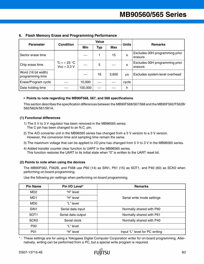
MB90560/565 Series
6. Flash Memory Erase and Programming Performance
• Points to note regarding the MB90F568, 567, and 568 specifications
This section describes the specification differences between the MB90F568/567/568 and the MB90F562/F562B/562/562A/561/561A.
(1) Functional differences
1) The 5 V to 3 V regulator has been removed in the MB96565 series.The C pin has been changed to an N.C. pin.
2) The A/D converter unit in the MB96565 series has changed from a 5 V version to a 3 V version.However, the conversion time and sampling time remain the same.
3) The maximum voltage that can be applied to I/O pins has changed from 5 V to 3 V in the MB96565 series.
4) Added transfer counter clear function to UART in the MB96565 series.This function restores the UART to its initial state when “0” is written to the UART reset bit.
(2) Points to note when using the devices
The MB90F562, F562B, and F568 use P60 (14) as SIN1, P61 (15) as SOT1, and P40 (60) as SCK0 whenperforming on-board programming.
Use the following pin settings when performing on-board programming.
* : These settings are for using a Yokogawa Digital Computer Corporation writer for on-board programming. Alter-natively, writing can be performed from a PC, but a special write program is required.
Parameter ConditionValue
Units RemarksMin Typ Max
Sector erase time
TA = + 25 °CVcc = 3.3 V
⎯ 1 15 sExcludes 00H programming prior erasure
Chip erase time ⎯ 5 ⎯ sExcludes 00H programming prior erasure
Word (16 bit width) programming time
⎯ 16 3,600 µs Excludes system-level overhead
Erase/Program cycle ⎯ 10,000 ⎯ ⎯ cycle
Data holding time ⎯ 100,000 ⎯ ⎯ h
Pin Name Pin I/O Level* Remarks
MD2 “H” level
Serial write mode settingsMD1 “H” level
MD0 “L” level
SIN1 Serial data input Normally shared with P60
SOT1 Serial data output Normally shared with P61
SCK0 Serial clock Normally shared with P40
P00 “L” level
P01 “H” level Input “L” level for PC writing
DS07-13715-4E 83

MB90560/565 Series
EXAMPLE CHARACTERISTICS
(Continued)
MB90F568 ICC − VCC
MB90568 ICC − VCC
MB90F568 ICCS − VCC
60
50
40
30
20
10
02 2.5 3 3.5
VCC (V)
ICC
(m
A)
4 4.5
16 MHz
12 MHz
8 MHz
4 MHz
2 MHz
TA = +25 °C
40
35
30
25
20
15
10
5
02 2.5 3 3.5
VCC (V)
ICC
3 (m
A)
4 4.5
16 MHz
12 MHz
8 MHz
4 MHz
2 MHz
TA = +25 °C
20
18
16
14
12
10
8
6
4
2
02 2.5 3 3.5
VCC (V)
ICC
S (
mA
)
4 4.5
16 MHz
12 MHz
8 MHz
4 MHz
2 MHz
TA = +25 °C
84 DS07-13715-4E

MB90560/565 Series
(Continued)
MB90568 ICCS − VCC
MB90F562 ICC − VCC
MB90562 ICC − VCC
18
16
14
12
10
8
6
4
2
02 2.5 3 3.5
VCC (V)
ICC
S (
mA
)
4 4.5
16 MHz
12 MHz
8 MHz
4 MHz
2 MHz
TA = +25 °C
2.5 3 3.5 4 4.5
VCC (V)5 5.5 6 6.5
ICC
(m
A)
f = 16 MHz
f = 12 MHz
f = 10 MHz
f = 8 MHz
f = 4 MHz
f = 2 MHz
40
35
30
25
20
15
10
5
0
TA = +25 °C
2.5 3 3.5 4 4.5
VCC (V)
5 5.5 6 6.5
ICC
(m
A)
70
60
50
40
30
20
10
0
f = 16 MHz
f = 12 MHz
f = 10 MHz
f = 8 MHz
f = 4 MHz
f = 2 MHz
TA = +25 °C
DS07-13715-4E 85

MB90560/565 Series
(Continued)
MB90F562 ICCS − VCC
MB90562 ICCS − VCC
2.5 3 3.5 4 4.5
VCC (V)5 5.5 6 6.5
ICC
S (
mA
)
16
14
12
10
8
6
4
2
0
f = 16 MHz
f = 12 MHz
f = 10 MHz
f = 8 MHz
f = 4 MHz
f = 2 MHz
TA = +25 °C
2.5 3 3.5 4 4.5VCC (V)
5 5.5 6 6.5
ICC
S (
mA
)
30
25
20
15
10
5
0
f = 16 MHz
f = 12 MHz
f = 10 MHz
f = 8 MHz
f = 4 MHz
f = 2 MHz
TA = +25 °C
86 DS07-13715-4E

MB90560/565 Series
ORDERING INFORMATION
• MB90560 series
• MB90565 series
Part No. Package Remarks
MB90561PMB90562PMB90561APMB90562APMB90F562PMB90F562BP
64-pin plastic SH-DIP (DIP-64P-M01)
MB90561PFMB90562PFMB90561APFMB90562APFMB90F562PFMB90F562BPF
64-pin plastic QFP (FPT-64P-M06)
MB90561PFMMB90562PFMMB90561APFMMB90562APFMMB90F562PFMMB90F562BPFM
64-pin plastic LQFP (FPT-64P-M09)
Part No. Package Remarks
MB90567PFMB90568PFMB90F568PF
64-pin plastic QFP (FPT-64P-M06)
MB90567PFMMB90568PFMMB90F568PFM
64-pin plastic LQFP (FPT-64P-M09)
DS07-13715-4E 87
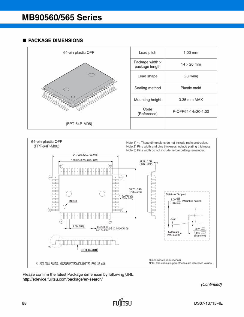
MB90560/565 Series
PACKAGE DIMENSIONS
Please confirm the latest Package dimension by following URL.http://edevice.fujitsu.com/package/en-search/
(Continued)
64-pin plastic QFP Lead pitch 1.00 mm
Package width ×package length
14 × 20 mm
Lead shape Gullwing
Sealing method Plastic mold
Mounting height 3.35 mm MAX
Code(Reference)
P-QFP64-14×20-1.00
64-pin plastic QFP(FPT-64P-M06)
(FPT-64P-M06)
C 2003-2008 FUJITSU MICROELECTRONICS LIMITED F64013S-c-5-6
0.20(.008) M
18.70±0.40(.736±.016)
14.00±0.20(.551±.008)
1.00(.039)
INDEX
0.10(.004)
1 19
20
3252
64
3351
20.00±0.20(.787±.008)
24.70±0.40(.972±.016)
0.42±0.08(.017±.003)
0.17±0.06(.007±.002)
0~8°
1.20±0.20(.047±.008)
3.00+0.35–0.20
(Mounting height).118
+.014–.008
0.25+0.15–0.20
.010+.006–.008
(Stand off)
Details of "A" part
"A"0.10(.004)
*
*
Dimensions in mm (inches).Note: The values in parentheses are reference values.
Note 1) * : These dimensions do not include resin protrusion.Note 2) Pins width and pins thickness include plating thickness.Note 3) Pins width do not include tie bar cutting remainder.
88 DS07-13715-4E

MB90560/565 Series
(Continued)
Please confirm the latest Package dimension by following URL.http://edevice.fujitsu.com/package/en-search/
64-pin plastic LQFP Lead pitch 0.65 mm
Package width ×package length
12 × 12 mm
Lead shape Gullwing
Sealing method Plastic mold
Mounting height 1.70 mm MAX
Code(Reference)
P-LQFP64-12×12-0.65
64-pin plastic LQFP(FPT-64P-M09)
(FPT-64P-M09)
C 2003-2008 FUJITSU MICROELECTRONICS LIMITED F64018S-c-3-6
0.65(.026)
0.10(.004)
1 16
17
3249
64
3348
12.00±0.10(.472±.004)SQ
14.00±0.20(.551±.008)SQ
INDEX
0.32±0.05(.013±.002)
M0.13(.005)
0.145±0.055(.0057±.0022)
"A"
.059 –.004+.008
–0.10+0.20
1.50
0~8°
0.25(.010)
(Mounting height)
0.50±0.20(.020±.008)0.60±0.15
(.024±.006)
0.10±0.10(.004±.004)
Details of "A" part
(Stand off)
0.10(.004)
*
Dimensions in mm (inches).Note: The values in parentheses are reference values.
Note 1) * : These dimensions do not include resin protrusion.Note 2) Pins width and pins thickness include plating thickness.Note 3) Pins width do not include tie bar cutting remainder.
DS07-13715-4E 89

MB90560/565 Series
MAIN CHANGES IN THIS EDITION
The vertical lines marked in the left side of the page show the changes.
Page Section Change Results
10 PIN DESCRIOTIONS Changed the circuit type of RST pin to H.
12Changed the circuit type of MD2 pin to B/I.Changed the “Description” of MD2 pin.
14 I/O CIRCUITS Added the Type H and Type I.
60 ELECTRICAL CHARACTERISTICS (MB90560 SERIES)3. DC Characteristics
Deleted the pin name MD0, MD1 of Pull-up resistor.
Added the “Only mask ROM product” in the remarks column of Pull-down resistor.
73 ELECTRICAL CHARACTERISTICS (MB90565 SERIES)3. DC Characteristics
Deleted the pin name MD0, MD1 of Pull-up resistor.
Added the “Only mask ROM product” in the remarks column of Pull-down resistor.
90 DS07-13715-4E
MB90560/565 Series
MEMO
DS07-13715-4E 91
MB90560/565 Series
FUJITSU MICROELECTRONICS LIMITED7-1, Nishishinjuku 2-chome, Shinjuku Dai-Ichi Seimei Bldg.,Shinjuku-ku, Tokyo 163-0722, JAPANTel: +81-3-5322-3347 Fax: +81-3-5322-3387http://jp.fujitsu.com/fml/en/
For further information please contact:
North and South AmericaFUJITSU MICROELECTRONICS AMERICA, INC.1250 E. Arques Avenue, M/S 333Sunnyvale, CA 94085-5401, U.S.A.Tel: +1-408-737-5600 Fax: +1-408-737-5999http://www.fma.fujitsu.com/
EuropeFUJITSU MICROELECTRONICS EUROPE GmbHPittlerstrasse 47, 63225 Langen, F. R. GERMANY Tel: +49-6103-690-0 Fax: +49-6103-690-122http://emea.fujitsu.com/microelectronics/
KoreaFUJITSU MICROELECTRONICS KOREA LTD.1002 Daechi-Dong, 206 KOSMO TOWER, Kangnam-Gu, Seoul 135-280, KOREATel: +82-2-3484-7100 Fax: +82-2-3484-7111http://www.fmk.fujitsu.com/
Asia PacificFUJITSU MICROELECTRONICS ASIA PTE LTD.151 Lorong Chuan, #05-08 New Tech Park,Singapore 556741, SINGAPORETel: +65-6281-0770 Fax: +65-6281-0220http://www.fujitsu.com/sg/services/micro/semiconductor/
FUJITSU MICROELECTRONICS SHANGHAI CO., LTD.No.222 Yan An Road(E), Rm.3102, Bund Center, Shanghai 200002, P. R. CHINATel: +86-21-6335-1560 Fax: +86-21-6335-1605http://cn.fujitsu.com/fmc/
FUJITSU MICROELECTRONICS PACIFIC ASIA LTD.11 Canton Road, 10/F., World Commerce Centre, Tsimshatsui, Kowloon, HONG KONGTel: +852-2377-0226 Fax: +852-2376-3269http://cn.fujitsu.com/fmc/tw
All Rights Reserved.
The contents of this document are subject to change without notice. Customers are advised to consult with sales representatives before ordering.The information, such as descriptions of function and application circuit examples, in this document are presented solely for the purposeof reference to show examples of operations and uses of FUJITSU MICROELECTRONICS device; FUJITSU MICROELECTRONICSdoes not warrant proper operation of the device with respect to use based on such information. When you develop equipment incorporat-ing the device based on such information, you must assume any responsibility arising out of such use of the information. FUJITSU MICROELECTRONICS assumes no liability for any damages whatsoever arising out of the use of the information.Any information in this document, including descriptions of function and schematic diagrams, shall not be construed as license of the useor exercise of any intellectual property right, such as patent right or copyright, or any other right of FUJITSU MICROELECTRONICSor any third party or does FUJITSU MICROELECTRONICS warrant non-infringement of any third-party's intellectual property right orother right by using such information. FUJITSU MICROELECTRONICS assumes no liability for any infringement of the intellectualproperty rights or other rights of third parties which would result from the use of information contained herein.The products described in this document are designed, developed and manufactured as contemplated for general use, including withoutlimitation, ordinary industrial use, general office use, personal use, and household use, but are not designed, developed and manufacturedas contemplated (1) for use accompanying fatal risks or dangers that, unless extremely high safety is secured, could have a serious effectto the public, and could lead directly to death, personal injury, severe physical damage or other loss (i.e., nuclear reaction control in nuclear facility, aircraft flight control, air traffic control, mass transport control, medical life support system, missile launch control inweapon system), or (2) for use requiring extremely high reliability (i.e., submersible repeater and artificial satellite).Please note that FUJITSU MICROELECTRONICS will not be liable against you and/or any third party for any claims or damages arisingin connection with above-mentioned uses of the products.Any semiconductor devices have an inherent chance of failure. You must protect against injury, damage or loss from such failures byincorporating safety design measures into your facility and equipment such as redundancy, fire protection, and prevention of over-currentlevels and other abnormal operating conditions.Exportation/release of any products described in this document may require necessary procedures in accordance with the regulations ofthe Foreign Exchange and Foreign Trade Control Law of Japan and/or US export control laws.The company names and brand names herein are the trademarks or registered trademarks of their respective owners.
Edited Business & Media Promotion Dept.


![[l5r 4e] Legend of the Five Rings 4E - Imperial Archives](https://static.fdocuments.us/doc/165x107/56d6cb291a28ab30169ca7a1/l5r-4e-legend-of-the-five-rings-4e-imperial-archives.jpg)


