
16-Bit, 160 MSPS 2x/4x/8x Interpolating Dual TxDAC+ D/A ... · 16-Bit, 160 MSPS 2x/4x/8x...
60
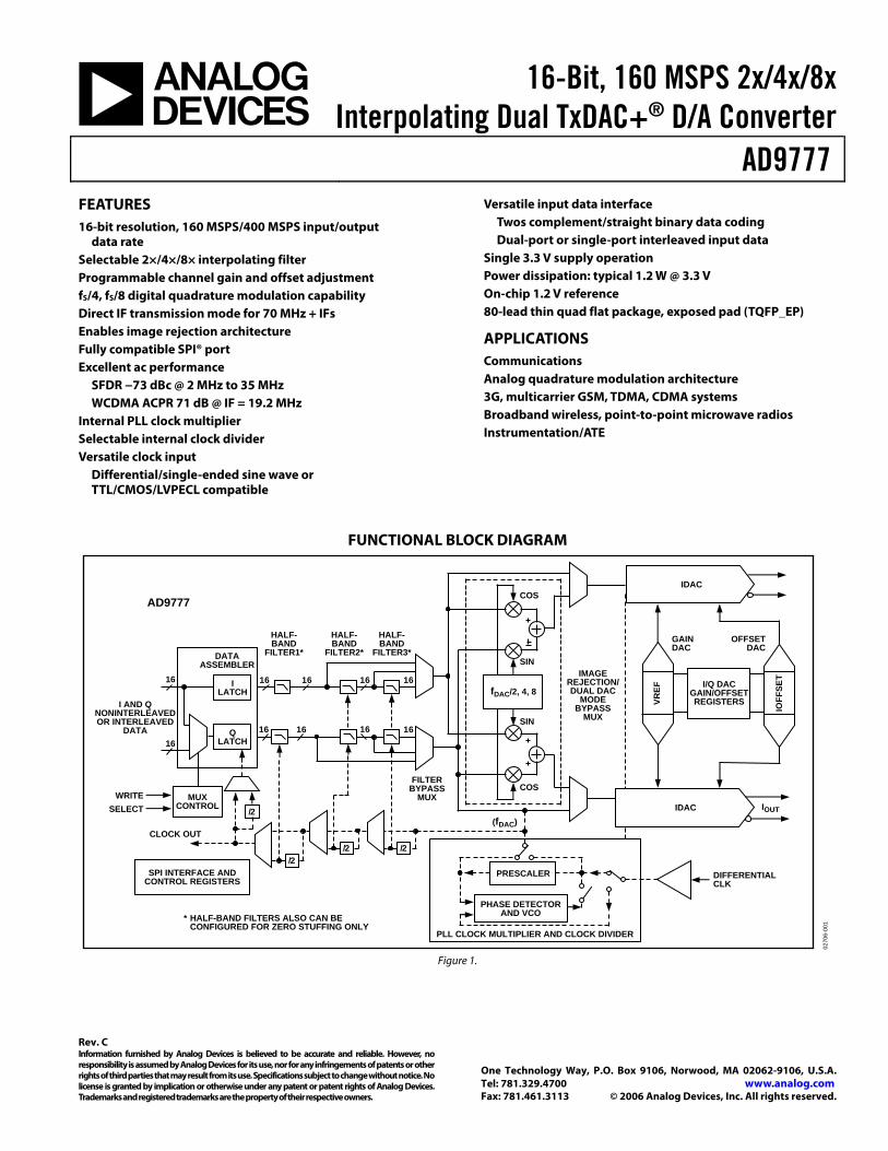
16-Bit, 160 MSPS 2x/4x/8x Interpolating Dual TxDAC+ ® D/A Converter AD9777 Rev. C Information furnished by Analog Devices is believed to be accurate and reliable. However, no responsibility is assumed by Analog Devices for its use, nor for any infringements of patents or other rights of third parties that may result from its use. Specifications subject to change without notice. No license is granted by implication or otherwise under any patent or patent rights of Analog Devices. Trademarks and registered trademarks are the property of their respective owners. One Technology Way, P.O. Box 9106, Norwood, MA 02062-9106, U.S.A. Tel: 781.329.4700 www.analog.com Fax: 781.461.3113 © 2006 Analog Devices, Inc. All rights reserved. FEATURES 16-bit resolution, 160 MSPS/400 MSPS input/output data rate Selectable 2×/4×/8× interpolating filter Programmable channel gain and offset adjustment fS/4, fS/8 digital quadrature modulation capability Direct IF transmission mode for 70 MHz + IFs Enables image rejection architecture Fully compatible SPI® port Excellent ac performance SFDR −73 dBc @ 2 MHz to 35 MHz WCDMA ACPR 71 dB @ IF = 19.2 MHz Internal PLL clock multiplier Selectable internal clock divider Versatile clock input Differential/single-ended sine wave or TTL/CMOS/LVPECL compatible Versatile input data interface Twos complement/straight binary data coding Dual-port or single-port interleaved input data Single 3.3 V supply operation Power dissipation: typical 1.2 W @ 3.3 V On-chip 1.2 V reference 80-lead thin quad flat package, exposed pad (TQFP_EP) APPLICATIONS Communications Analog quadrature modulation architecture 3G, multicarrier GSM, TDMA, CDMA systems Broadband wireless, point-to-point microwave radios Instrumentation/ATE FUNCTIONAL BLOCK DIAGRAM 16 16 16 /2 16 16 16 16 16 /2 /2 /2 AD9777 DATA ASSEMBLER I LATCH Q LATCH MUX CONTROL SPI INTERFACE AND CONTROL REGISTERS HALF-BAND FILTERS ALSO CAN BE CONFIGURED FOR ZERO STUFFING ONLY * I AND Q NONINTERLEAVED OR INTERLEAVED DATA 16 16 CLOCK OUT WRITE SELECT HALF- BAND FILTER1* FILTER BYPASS MUX IMAGE REJECTION/ DUAL DAC MODE BYPASS MUX I/Q DAC GAIN/OFFSET REGISTERS HALF- BAND FILTER2* HALF- BAND FILTER3* COS IDAC IDAC VREF IOFFSET GAIN DAC DIFFERENTIAL CLK OFFSET DAC COS I OUT PRESCALER PLL CLOCK MULTIPLIER AND CLOCK DIVIDER PHASE DETECTOR AND VCO SIN SIN f DAC /2, 4, 8 (f DAC ) 02706-001 Figure 1.
-
Upload
truongdang -
Category
Documents
-
view
223 -
download
0
Transcript of 16-Bit, 160 MSPS 2x/4x/8x Interpolating Dual TxDAC+ D/A ... · 16-Bit, 160 MSPS 2x/4x/8x...
16-Bit, 160 MSPS 2x/4x/8xInterpolating Dual TxDAC+® D/A Converter
AD9777
Rev. C Information furnished by Analog Devices is believed to be accurate and reliable. However, no responsibility is assumed by Analog Devices for its use, nor for any infringements of patents or other rights of third parties that may result from its use. Specifications subject to change without notice. No license is granted by implication or otherwise under any patent or patent rights of Analog Devices. Trademarks and registered trademarks are the property of their respective owners.
One Technology Way, P.O. Box 9106, Norwood, MA 02062-9106, U.S.A.Tel: 781.329.4700 www.analog.com Fax: 781.461.3113 © 2006 Analog Devices, Inc. All rights reserved.
FEATURES 16-bit resolution, 160 MSPS/400 MSPS input/output
data rate Selectable 2×/4×/8× interpolating filter Programmable channel gain and offset adjustment fS/4, fS/8 digital quadrature modulation capability Direct IF transmission mode for 70 MHz + IFs Enables image rejection architecture Fully compatible SPI® port Excellent ac performance
SFDR −73 dBc @ 2 MHz to 35 MHz WCDMA ACPR 71 dB @ IF = 19.2 MHz
Internal PLL clock multiplier Selectable internal clock divider Versatile clock input
Differential/single-ended sine wave or TTL/CMOS/LVPECL compatible
Versatile input data interface Twos complement/straight binary data coding Dual-port or single-port interleaved input data
Single 3.3 V supply operation Power dissipation: typical 1.2 W @ 3.3 V On-chip 1.2 V reference 80-lead thin quad flat package, exposed pad (TQFP_EP)
APPLICATIONS Communications Analog quadrature modulation architecture 3G, multicarrier GSM, TDMA, CDMA systems Broadband wireless, point-to-point microwave radios Instrumentation/ATE
FUNCTIONAL BLOCK DIAGRAM
16
1616
/2
161616
1616
/2/2 /2
AD9777
DATAASSEMBLER
ILATCH
QLATCH
MUXCONTROL
SPI INTERFACE ANDCONTROL REGISTERS
HALF-BAND FILTERS ALSO CAN BECONFIGURED FOR ZERO STUFFING ONLY
*
I AND QNONINTERLEAVEDOR INTERLEAVED
DATA
16
16
CLOCK OUT
WRITESELECT
HALF-BAND
FILTER1*
FILTERBYPASS
MUX
IMAGEREJECTION/DUAL DAC
MODEBYPASS
MUX
I/Q DACGAIN/OFFSETREGISTERS
HALF-BAND
FILTER2*
HALF-BAND
FILTER3*
COSIDAC
IDAC
VREF
IOFF
SET
GAINDAC
DIFFERENTIALCLK
OFFSETDAC
COS
IOUT
PRESCALER
PLL CLOCK MULTIPLIER AND CLOCK DIVIDER
PHASE DETECTORAND VCO
SIN
SIN
fDAC/2, 4, 8
(fDAC)02
706-
001
Figure 1.
AD9777
Rev. C | Page 2 of 60
TABLE OF CONTENTS Features .............................................................................................. 1 Applications....................................................................................... 1 General Description ......................................................................... 4
Product Highlights ....................................................................... 4 Specifications..................................................................................... 5
DC Specifications ......................................................................... 5 Dynamic Specifications ............................................................... 6 Digital Specifications ................................................................... 7 Digital Filter Specifications ......................................................... 8
Absolute Maximum Ratings............................................................ 9 Thermal Characteristics .............................................................. 9 ESD Caution.................................................................................. 9
Pin Configuration and Function Descriptions........................... 10 Terminology .................................................................................... 12 Typical Performance Characteristics ........................................... 13
Mode Control (via SPI Port) ..................................................... 18 Register Description................................................................... 20
Functional Description .................................................................. 22 Serial Interface for Register Control ........................................ 22 General Operation of the Serial Interface ............................... 22 Instruction Byte .......................................................................... 23 R/W .............................................................................................. 23 N1, N0.......................................................................................... 23 A4, A3, A2, A1, A0..................................................................... 23 Serial Interface Port Pin Descriptions ..................................... 23 MSB/LSB Transfers..................................................................... 23 Notes on Serial Port Operation ................................................ 25 DAC Operation........................................................................... 25 1R/2R Mode ................................................................................ 26 CLOCK Input Configuration ................................................... 26 Programmable PLL .................................................................... 27 Power Dissipation....................................................................... 29
Sleep/Power-Down Modes........................................................ 29 Two Port Data Input Mode ....................................................... 29 PLL Enabled, Two-Port Mode .................................................. 30 DATACLK Inversion.................................................................. 30 DATACLK Driver Strength....................................................... 30 PLL Enabled, One-Port Mode .................................................. 30 ONEPORTCLK Inversion......................................................... 31 ONEPORTCLK Driver Strength.............................................. 31 IQ Pairing .................................................................................... 31 PLL Disabled, Two-Port Mode................................................. 31 PLL Disabled, One-Port Mode ................................................. 32 Digital Filter Modes ................................................................... 32 Amplitude Modulation.............................................................. 32 Modulation, No Interpolation .................................................. 34 Modulation, Interpolation = 2× ............................................... 35 Modulation, Intermodulation = 4× ......................................... 36 Modulation, Intermodulation = 8× ......................................... 37 Zero Stuffing ............................................................................... 38 Interpolating (Complex Mix Mode)........................................ 38 Operations on Complex Signals............................................... 38 Complex Modulation and Image Rejection of Baseband Signals .......................................................................................... 39 Image Rejection and Sideband Suppressions of Modulated Carriers ........................................................................................ 41
Applying the Output Configurations........................................... 46 Unbuffered Differential Output, Equivalent Circuit ............. 46 Differential Coupling Using a Transformer............................ 46 Differential Coupling Using an Op Amp................................ 47 Interfacing with the AD8345 Quadrature Modulator........... 47
Evaluation Board ............................................................................ 48 Outline Dimensions ....................................................................... 58
Ordering Guide .......................................................................... 58
AD9777
Rev. C | Page 3 of 60
REVISION HISTORY
1/06—Rev. B to Rev. C Updated Formatting .........................................................Universal Changes to Figure 32 .................................................................... 22 Changes to Figure 108 .................................................................. 54 Updated Outline Dimensions ..................................................... 58 Changes to Ordering Guide......................................................... 58
6/04—Data Sheet Changed from Rev. A to Rev. B. Changes to DC Specifications ....................................................... 5 Changes to Absolute Maximum Ratings...................................... 8 Changes to DAC Operation Section........................................... 25 Changes to Figure 49, Figure 50, and Figure 51........................ 29 Changes to the PLL Enabled, One-Port Mode Section............ 30 Changes to the PLL Disabled, One-Port Mode Section........... 32 Changes to the Ordering Guide .................................................. 57 Updated the Outline Dimensions ............................................... 57
3/03—Data Sheet Changed from Rev. 0 to Rev. A. Edits to Features .............................................................................. 1 Edits to DC Specifications ............................................................. 3 Edits to Dynamic Specifications.................................................... 4 Edits to Pin Function Descriptions............................................... 7 Edits to Table I ............................................................................... 14 Edits to Register Description—Address 02h Section ............... 15 Edits to Register Description—Address 03h Section ............... 16
Edits to Register Description—Address 07h, 0Bh Section...... 16 Edits to Equation 1........................................................................ 16 Edits to MSB/LSB Transfers Section........................................... 18 Changes to Figure 8 ...................................................................... 20 Edits to Programmable PLL Section........................................... 21 Added new Figure 14.................................................................... 22 Renumbered Figures 15 to 69...................................................... 22 Added Two-Port Data Input Mode Section............................... 23 Edits to PLL Enabled, Two-Port Mode Section ........................ 24 Edits to Figure 19 ......................................................................... 24 Edits to Figure 21 .......................................................................... 25 Edits to PLL Disabled, Two-Port Mode Section ....................... 25 Edits to Figure 22 .......................................................................... 25 Edits to Figure 23 .......................................................................... 26 Edits to Figure 26a ........................................................................ 27 Changes to Figures 53 and 54...................................................... 38 Edits to Evaluation Board Section .............................................. 39 Changes to Figures 56 to 59......................................................... 40 Replaced Figures 60 to 69 ............................................................ 42 Updated Outline Dimensions...................................................... 49
7/02—Revision 0: Initial Version
AD9777
Rev. C | Page 4 of 60
GENERAL DESCRIPTIONThe AD97771 is the 16-bit member of the AD977x pin compatible, high performance, programmable 2×/4×/8× interpolating TxDAC+ family. The AD977x family features a serial port interface (SPI) that provides a high level of programmability, thus allowing for enhanced system level options. These options include selectable 2×/4×/8× interpola-tion filters; fS/2, fS/4, or fS/8 digital quadrature modulation with image rejection; a direct IF mode; programmable channel gain and offset control; programmable internal clock divider; straight binary or twos complement data interface; and a single-port or dual-port data interface.
The selectable 2×/4×/8× interpolation filters simplify the requirements of the reconstruction filters while simultaneously enhancing the TxDAC+ family’s pass-band noise/distortion performance. The independent channel gain and offset adjust registers allow the user to calibrate LO feedthrough and sideband suppression errors associated with analog quadrature modulators. The 6 dB of gain adjustment range can also be used to control the output power level of each DAC.
The AD9777 features the ability to perform fS/2, fS/4, and fS/8 digital modulation and image rejection when combined with an analog quadrature modulator. In this mode, the AD9777 accepts I and Q complex data (representing a single or multicarrier wave-form), generates a quadrature modulated IF signal along with its orthogonal representation via its dual DACs, and presents these two reconstructed orthogonal IF carriers to an analog quadrature modulator to complete the image rejection upconversion process. Another digital modulation mode (that is, the direct IF mode) allows the original baseband signal representation to be fre-quency translated such that pairs of images fall at multiples of one-half the DAC update rate.
The AD977x family includes a flexible clock interface accepting differential or single-ended sine wave or digital logic inputs. An internal PLL clock multiplier is included and generates the necessary on-chip high frequency clocks. It can also be disabled to allow the use of a higher performance external clock source. An internal programmable divider simplifies clock generation in the converter when using an external clock source. A flexible data input interface allows for straight binary or twos comple-ment formats and supports single-port interleaved or dual-port data.
Dual high performance DAC outputs provide a differential current output programmable over a 2 mA to 20 mA range. The AD9777 is manufactured on an advanced 0.35 micron CMOS process, operates from a single-supply of 3.1 V to 3.5 V, and consumes 1.2 W of power.
1 Protected by U.S. Patent Numbers, 5,568,145; 5,689,257; and 5,703,519.
Other patents pending.
Targeted at wide dynamic range, multicarrier, and multistandard systems, the superb baseband performance of the AD9777 is ideal for wideband CDMA, multicarrier CDMA, multicarrier TDMA, multicarrier GSM, and high performance systems employing high-order QAM modulation schemes. The image rejection feature simplifies and can help to reduce the number of signal band filters needed in a transmit signal chain. The direct IF mode helps to eliminate a costly mixer stage for a variety of communications systems.
PRODUCT HIGHLIGHTS
1. The AD9777 is the 16-bit member of the AD977x pin compatible, high performance, programmable 2×/4×/8× interpolating TxDAC+ family.
2. Direct IF transmission is possible for 70 MHz + IFs through a novel digital mixing process.
3. fS/2, fS/4, and fS/8 digital quadrature modulation and user selectable image rejection simplify/remove cascaded SAW filter stages.
4. A 2×/4×/8× user selectable interpolating filter eases data rate and output signal reconstruction filter requirements.
5. User selectable twos complement/straight binary data coding.
6. User programmable channel gain control over 1 dB range in 0.01 dB increments.
7. User programmable channel offset control ±10% over the FSR.
8. Ultrahigh speed 400 MSPS DAC conversion rate.
9. Internal clock divider provides data rate clock for easy interfacing.
10. Flexible clock input with single-ended or differential input, CMOS, or 1 V p-p LO sine wave input capability.
11. Low power: Complete CMOS DAC operates on 1.2 W from a 3.1 V to 3.5 V single supply. The 20 mA full-scale current can be reduced for lower power operation, and several sleep functions are provided to reduce power during idle periods.
12. On-chip voltage reference: The AD9777 includes a 1.20 V temperature compensated band gap voltage reference.
13. An 80-lead thin quad flat package, exposed pad (TQFP_EP).
AD9777
Rev. C | Page 5 of 60
SPECIFICATIONS DC SPECIFICATIONS TMIN to TMAX, AVDD = 3.3 V, CLKVDD = 3.3 V, DVDD = 3.3 V, PLLVDD = 3.3 V, IOUTFS = 20 mA, unless otherwise noted.
Table 1. Parameter Min Typ Max Unit RESOLUTION 16 Bits
DC Accuracy1 Integral Nonlinearity ±6 LSB Differential Nonlinearity −6.5 ±3 +6.5 LSB
ANALOG OUTPUT (for 1R and 2R Gain Setting Modes) Offset Error −0.025 ±0.01 +0.025 % of FSR Gain Error (with Internal Reference) −1.0 +1.0 % of FSR Gain Matching −1 ±0.1 +1 % of FSR Full-Scale Output Current2 2 20 mA Output Compliance Range −1.0 +1.25 V Output Resistance 200 kΩ Output Capacitance 3 pF Gain, Offset Cal DACs, Monotonicity Guaranteed
REFERENCE OUTPUT Reference Voltage 1.14 1.20 1.26 V Reference Output Current3 100 nA
REFERENCE INPUT Input Compliance Range 0.1 1.25 V Reference Input Resistance 7 kΩ Small Signal Bandwidth 0.5 MHz
TEMPERATURE COEFFICIENTS Offset Drift 0 ppm of FSR/°C Gain Drift (with Internal Reference) 50 ppm of FSR/°C Reference Voltage Drift ±50 ppm/°C
POWER SUPPLY AVDD
Voltage Range 3.1 3.3 3.5 V Analog Supply Current (IAVDD)4 72.5 76 mA IAVDD in SLEEP Mode 23.3 26 mA
CLKVDD (PLL OFF) Voltage Range 3.1 3.3 3.5 V Clock Supply Current (ICLKVDD)4 8.5 10.0 mA
CLKVDD (PLL ON) Clock Supply Current (ICLKVDD) 23.5 mA
DVDD Voltage Range 3.1 3.3 3.5 V Digital Supply Current (IDVDD)4 34 41 mA Nominal Power Dissipation4 380 410 mW PDIS
5 1.75 W PDIS in PWDN 6.0 mW
Power Supply Rejection Ratio—AVDD ±0.4 % of FSR/V OPERATING RANGE −40 +85 °C 1 Measured at IOUTA driving a virtual ground. 2 Nominal full-scale current, IOUTFS, is 32× the IREF current. 3 Use an external amplifier to drive any external load. 4 100 MSPS fDAC with fOUT = 1 MHz, all supplies = 3.3 V, no interpolation, no modulation. 5 400 MSPS fDAC, fDATA = 50 MSPS, fS/2 modulation, PLL enabled.
AD9777
Rev. C | Page 6 of 60
DYNAMIC SPECIFICATIONS TMIN to TMAX, AVDD = 3.3 V, CLKVDD = 3.3 V, DVDD = 3.3 V, PLLVDD = 0 V, IOUTFS = 20 mA, Interpolation = 2×, differential transformer-coupled output, 50 Ω doubly terminated, unless otherwise noted.
Table 2. Parameter Min Typ Max Unit DYNAMIC PERFORMANCE
Maximum DAC Output Update Rate (fDAC) 400 MSPS Output Settling Time (tST) (to 0.025%) 11 ns Output Rise Time (10% to 90%)1 0.8 ns Output Fall Time (10% to 90%)1 0.8 ns Output Noise (IOUTFS = 20 mA) 50 pA/√Hz
AC LINEARITY—BASEBAND MODE Spurious-Free Dynamic Range (SFDR) to Nyquist (fOUT = 0 dBFS)
fDATA = 100 MSPS, fOUT = 1 MHz 71 85 dBc fDATA = 65 MSPS, fOUT = 1 MHz 85 dBc fDATA = 65 MSPS, fOUT = 15 MHz 84 dBc fDATA = 78 MSPS, fOUT = 1 MHz 85 dBc fDATA = 78 MSPS, fOUT = 15 MHz 83 dBc fDATA = 160 MSPS, fOUT = 1 MHz 85 dBc fDATA = 160 MSPS, fOUT = 15 MHz 83 dBc
Spurious-Free Dynamic Range within a 1 MHz Window fOUT = 0 dBFS, fDATA = 100 MSPS, fOUT = 1 MHz 73 99.1 dBc
Two-Tone Intermodulation (IMD) to Nyquist (fOUT1 = fOUT2 = −6 dBFS) fDATA = 65 MSPS, fOUT1 = 10 MHz; fOUT2 = 11 MHz 85 dBc fDATA = 65 MSPS, fOUT1 = 20 MHz; fOUT2 = 21 MHz 78 dBc fDATA = 78 MSPS, fOUT1 = 10 MHz; fOUT2 = 11 MHz 85 dBc fDATA = 78 MSPS, fOUT1 = 20 MHz; fOUT2 = 21 MHz 78 dBc fDATA = 160 MSPS, fOUT1 = 10 MHz; fOUT2 = 11 MHz 85 dBc fDATA = 160 MSPS, fOUT1 = 20 MHz; fOUT2 = 21 MHz 84 dBc
Total Harmonic Distortion (THD) fDATA = 100 MSPS, fOUT = 1 MHz; 0 dBFS −71 −83 dB
Signal-to-Noise Ratio (SNR) fDATA = 78 MSPS, fOUT = 5 MHz; 0 dBFS 79 dB fDATA = 160 MSPS, fOUT = 5 MHz; 0 dBFS 75 dB
Adjacent Channel Power Ratio (ACPR) WCDMA with 3.84 MHz BW, 5 MHz Channel Spacing IF = Baseband, fDATA = 76.8 MSPS 73 dBc IF = 19.2 MHz, fDATA = 76.8 MSPS 73 dBc
Four-Tone Intermodulation 21 MHz, 22 MHz, 23 MHz, and 24 MHz at −12 dBFS (fDATA = MSPS, Missing Center) 76 dBFS
AC LINEARITY—IF MODE Four-Tone Intermodulation at IF = 200 MHz
201 MHz, 202 MHz, 203 MHz, and 204 MHz at −12 dBFS (fDATA = 160 MSPS, fDAC = 320 MHz) 72 dBFS 1 Measured single-ended into 50 Ω load.
AD9777
Rev. C | Page 7 of 60
DIGITAL SPECIFICATIONS TMIN to TMAX, AVDD = 3.3 V, CLKVDD = 3.3 V, PLLVDD = 0 V, DVDD = 3.3 V, IOUTFS = 20 mA, unless otherwise noted.
Table 3. Parameter Min Typ Max Unit DIGITAL INPUTS
Logic 1 Voltage 2.1 3 V Logic 0 Voltage 0 0.9 V Logic 1 Current −10 +10 µA Logic 0 Current −10 +10 µA Input Capacitance 5 pF
CLOCK INPUTS Input Voltage Range 0 3 V Common-Mode Voltage 0.75 1.5 2.25 V Differential Voltage 0.5 1.5 V
SERIAL CONTROL BUS Maximum SCLK Frequency (fSLCK) 15 MHz Mimimum Clock Pulse Width High (tPWH) 30 ns Mimimum Clock Pulse Width Low (tPWL) 30 ns Maximum Clock Rise/Fall Time 1 ms Minimum Data/Chip Select Setup Time (tDS) 25 ns Minimum Data Hold Time (tDH) 0 ns Maximum Data Valid Time (tDV) 30 ns RESET Pulse Width 1.5 ns
Inputs (SDI, SDIO, SCLK, CSB) Logic 1 Voltage 2.1 3 V Logic 0 Voltage 0 0.9 V Logic 1 Current −10 +10 µA Logic 0 Current −10 +10 µA Input Capacitance 5 pF
SDIO Output Logic 1 Voltage DRVDD − 0.6 V Logic 0 Voltage 0.4 V Logic 1 Current 30 50 mA Logic 0 Current 30 50 mA
AD9777
Rev. C | Page 8 of 60
DIGITAL FILTER SPECIFICATIONS
Table 4. Half-Band Filter No. 1 (43 Coefficients) Tap Coefficient 1, 43 8 2, 42 0 3, 41 −29 4, 40 0 5, 39 67 6, 38 0 7, 37 −134 8, 36 0 9, 35 244 10, 34 0 11, 33 −414 12, 32 0 13, 31 673 14, 30 0 15, 29 −1,079 16, 28 0 17, 27 1,772 18, 26 0 19, 25 −3,280 20, 24 0 21, 23 10,364 22 16,384
Table 5. Half-Band Filter No. 2 (19 Coefficients) Tap Coefficient 1, 19 19 2, 18 0 3, 17 −120 4, 16 0 5, 15 438 6, 14 0 7, 13 −1,288 8, 12 0 9, 11 5,047 10 8,192
Table 6. Half-Band Filter No. 3 (11 Coefficients) Tap Coefficient 1, 11 7 2, 10 0 3, 9 −53 4, 8 0 5, 7 302 6 512
–120
–100
–80
–60
–40
–20
0
20
ATT
ENU
ATI
ON
(dB
FS)
fOUT (NORMALIZED TO INPUT DATA RATE)
0.50 1.0 1.5 2.0
0270
6-00
3
Figure 2. 2× Interpolating Filter Response
–120
–100
–80
–60
–40
–20
0
20
ATT
ENU
ATI
ON
(dB
FS)
fOUT (NORMALIZED TO INPUT DATA RATE)
0.50 1.0 1.5 2.0
0270
6-00
4
Figure 3. 4× Interpolating Filter Response
–120
–100
–80
–60
–40
–20
0
20
ATT
ENU
ATI
ON
(dB
FS)
fOUT (NORMALIZED TO INPUT DATA RATE)
20 4 6
0270
6-00
58
Figure 4. 8× Interpolating Filter Response
AD9777
Rev. C | Page 9 of 60
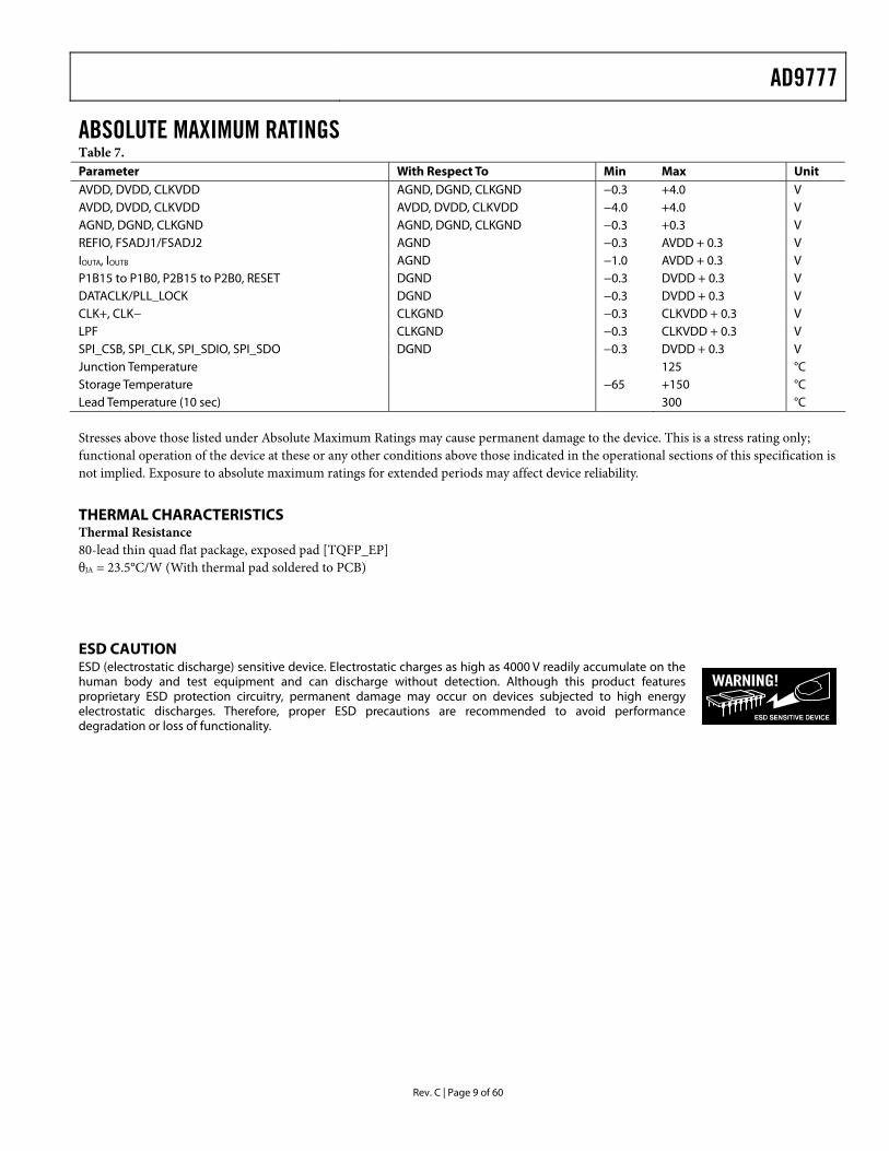
ABSOLUTE MAXIMUM RATINGS Table 7. Parameter With Respect To Min Max Unit AVDD, DVDD, CLKVDD AGND, DGND, CLKGND −0.3 +4.0 V AVDD, DVDD, CLKVDD AVDD, DVDD, CLKVDD −4.0 +4.0 V AGND, DGND, CLKGND AGND, DGND, CLKGND −0.3 +0.3 V REFIO, FSADJ1/FSADJ2 AGND −0.3 AVDD + 0.3 V IOUTA, IOUTB AGND −1.0 AVDD + 0.3 V P1B15 to P1B0, P2B15 to P2B0, RESET DGND −0.3 DVDD + 0.3 V DATACLK/PLL_LOCK DGND −0.3 DVDD + 0.3 V CLK+, CLK− CLKGND −0.3 CLKVDD + 0.3 V LPF CLKGND −0.3 CLKVDD + 0.3 V SPI_CSB, SPI_CLK, SPI_SDIO, SPI_SDO DGND −0.3 DVDD + 0.3 V Junction Temperature 125 °C Storage Temperature −65 +150 °C Lead Temperature (10 sec) 300 °C
Stresses above those listed under Absolute Maximum Ratings may cause permanent damage to the device. This is a stress rating only; functional operation of the device at these or any other conditions above those indicated in the operational sections of this specification is not implied. Exposure to absolute maximum ratings for extended periods may affect device reliability.
THERMAL CHARACTERISTICS Thermal Resistance 80-lead thin quad flat package, exposed pad [TQFP_EP] θJA = 23.5°C/W (With thermal pad soldered to PCB)
ESD CAUTION ESD (electrostatic discharge) sensitive device. Electrostatic charges as high as 4000 V readily accumulate on the human body and test equipment and can discharge without detection. Although this product features proprietary ESD protection circuitry, permanent damage may occur on devices subjected to high energy electrostatic discharges. Therefore, proper ESD precautions are recommended to avoid performance degradation or loss of functionality.
AD9777
Rev. C | Page 10 of 60
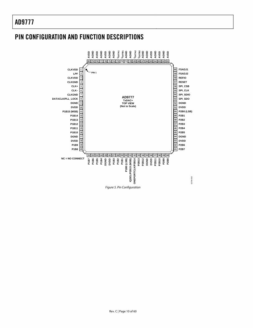
PIN CONFIGURATION AND FUNCTION DESCRIPTIONS
FSADJ1FSADJ2REFIORESETSPI_CSBSPI_CLKSPI_SDIOSPI_SDODGNDDVDDP2B0 (LSB)P2B1P2B2P2B3P2B4P2B5DGNDDVDDP2B6P2B7
0270
6-00
2
2
3
4
7
6
5
1
8
9
10
12
13
14
15
16
17
18
19
20
11
59
58
57
54
55
56
60
53
52
51
49
48
47
46
45
44
43
42
41
50
PIN 1
NC = NO CONNECT21 22 23 24 25 26 27 28 29 30 31 32 33 34 35 36 37 38 39 40
80 79 78 77 76 75 74 73 72 71 70 69 68 67 66 65 64 63 62 61
AD9777TxDAC+
TOP VIEW(Not to Scale)
AVD
D
AVD
D
AVD
D
AG
ND
AG
ND
AG
ND
AG
ND
AG
ND
AG
ND
AG
ND
AG
ND
AG
ND
AG
ND
AVD
D
AVD
D
AVD
D
I OU
TA1
I OU
TA2
I OU
TB2
I OU
TB1
P1B
7P1
B6
P1B
5P1
B4
DG
ND
DVD
DP1
B3
P1B
2P1
B1
P1B
0 (L
SB)
IQSE
L/P2
B15
(MSB
)O
NEP
OR
TCLK
/P2B
14P2
B13
P2B
12D
GN
DD
VDD
P2B
11P2
B10
P2B
9P2
B8
CLKVDDLPF
CLKVDDCLKGND
CLK+CLK–
CLKGNDDATACLK/PLL_LOCK
DGNDDVDD
P1B15 (MSB)P1B14P1B13P1B12P1B11P1B10DGNDDVDDP1B9P1B8
Figure 5. Pin Configuration
AD9777
Rev. C | Page 11 of 60
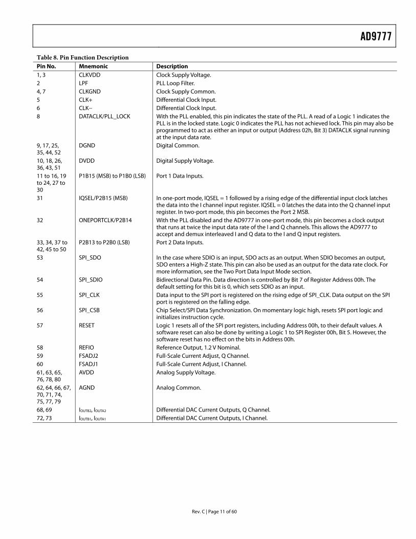
Table 8. Pin Function Description Pin No. Mnemonic Description 1, 3 CLKVDD Clock Supply Voltage. 2 LPF PLL Loop Filter. 4, 7 CLKGND Clock Supply Common. 5 CLK+ Differential Clock Input. 6 CLK− Differential Clock Input. 8 DATACLK/PLL_LOCK With the PLL enabled, this pin indicates the state of the PLL. A read of a Logic 1 indicates the
PLL is in the locked state. Logic 0 indicates the PLL has not achieved lock. This pin may also be programmed to act as either an input or output (Address 02h, Bit 3) DATACLK signal running at the input data rate.
9, 17, 25, 35, 44, 52
DGND Digital Common.
10, 18, 26, 36, 43, 51
DVDD Digital Supply Voltage.
11 to 16, 19 to 24, 27 to 30
P1B15 (MSB) to P1B0 (LSB) Port 1 Data Inputs.
31 IQSEL/P2B15 (MSB) In one-port mode, IQSEL = 1 followed by a rising edge of the differential input clock latches the data into the I channel input register. IQSEL = 0 latches the data into the Q channel input register. In two-port mode, this pin becomes the Port 2 MSB.
32 ONEPORTCLK/P2B14 With the PLL disabled and the AD9777 in one-port mode, this pin becomes a clock output that runs at twice the input data rate of the I and Q channels. This allows the AD9777 to accept and demux interleaved I and Q data to the I and Q input registers.
33, 34, 37 to 42, 45 to 50
P2B13 to P2B0 (LSB) Port 2 Data Inputs.
53 SPI_SDO In the case where SDIO is an input, SDO acts as an output. When SDIO becomes an output, SDO enters a High-Z state. This pin can also be used as an output for the data rate clock. For more information, see the Two Port Data Input Mode section.
54 SPI_SDIO Bidirectional Data Pin. Data direction is controlled by Bit 7 of Register Address 00h. The default setting for this bit is 0, which sets SDIO as an input.
55 SPI_CLK Data input to the SPI port is registered on the rising edge of SPI_CLK. Data output on the SPI port is registered on the falling edge.
56 SPI_CSB Chip Select/SPI Data Synchronization. On momentary logic high, resets SPI port logic and initializes instruction cycle.
57 RESET Logic 1 resets all of the SPI port registers, including Address 00h, to their default values. A software reset can also be done by writing a Logic 1 to SPI Register 00h, Bit 5. However, the software reset has no effect on the bits in Address 00h.
58 REFIO Reference Output, 1.2 V Nominal. 59 FSADJ2 Full-Scale Current Adjust, Q Channel. 60 FSADJ1 Full-Scale Current Adjust, I Channel. 61, 63, 65, 76, 78, 80
AVDD Analog Supply Voltage.
62, 64, 66, 67, 70, 71, 74, 75, 77, 79
AGND Analog Common.
68, 69 IOUTB2, IOUTA2 Differential DAC Current Outputs, Q Channel. 72, 73 IOUTB1, IOUTA1 Differential DAC Current Outputs, I Channel.

AD9777
Rev. C | Page 12 of 60
TERMINOLOGY Adjacent Channel Power Ratio (ACPR) A ratio in dBc between the measured power within a channel relative to its adjacent channel.
Complex Image Rejection In a traditional two-part upconversion, two images are created around the second IF frequency. These images are redundant and have the effect of wasting transmitter power and system bandwidth. By placing the real part of a second complex modulator in series with the first complex modulator, either the upper or lower frequency image near the second IF can be rejected.
Complex Modulation The process of passing the real and imaginary components of a signal through a complex modulator (transfer function = ejωt = cosωt + jsinωt) and realizing real and imaginary components on the modulator output.
Differential Nonlinearity (DNL) DNL is the measure of the variation in analog value, normalized to full scale, associated with a 1 LSB change in digital input code.
Gain Error The difference between the actual and ideal output span. The actual span is determined by the output when all inputs are set to 1 minus the output when all inputs are set to 0.
Glitch Impulse Asymmetrical switching times in a DAC give rise to undesired output transients that are quantified by a glitch impulse. It is specified as the net area of the glitch in pV-s.
Group Delay Number of input clocks between an impulse applied at the device input and the peak DAC output current. A half-band FIR filter has constant group delay over its entire frequency range.
Impulse Response Response of the device to an impulse applied to the input.
Interpolation Filter If the digital inputs to the DAC are sampled at a multiple rate of fDATA (interpolation rate), a digital filter can be constructed that has a sharp transition band near fDATA/2. Images that would typically appear around fDAC (output data rate) can be greatly suppressed.
Linearity Error (Also called integral nonlinearity or INL) Linearity error is defined as the maximum deviation of the actual analog output from the ideal output, determined by a straight line drawn from zero to full scale.
Monotonicity A DAC is monotonic if the output either increases or remains constant as the digital input increases.
Offset Error The deviation of the output current from the ideal of 0 is called offset error. For IOUTA, 0 mA output is expected when the inputs are all 0. For IOUTB, 0 mA output is expected when all inputs are set to 1.
Output Compliance Range The range of allowable voltage at the output of a current-output DAC. Operation beyond the maximum compliance limits may cause either output stage saturation or breakdown, resulting in nonlinear performance.
Pass Band Frequency band in which any input applied therein passes unattenuated to the DAC output.
Power Supply Rejection The maximum change in the full-scale output as the supplies are varied from minimum to maximum specified voltages.
Signal-to-Noise Ratio (SNR) SNR is the ratio of the rms value of the measured output signal to the rms sum of all other spectral components below the Nyquist frequency, excluding the first six harmonics and dc. The value for SNR is expressed in decibels.
Spurious-Free Dynamic Range The difference, in dB, between the rms amplitude of the output signal and the peak spurious signal over the specified bandwidth.
Settling Time The time required for the output to reach and remain within a specified error band about its final value, measured from the start of the output transition.
Stop-Band Rejection The amount of attenuation of a frequency outside the pass band applied to the DAC, relative to a full-scale signal applied at the DAC input within the pass band.
Temperature Drift It is specified as the maximum change from the ambient (25°C) value to the value at either TMIN or TMAX. For offset and gain drift, the drift is reported in ppm of full-scale range (FSR) per °C. For reference drift, the drift is reported in ppm per °C.
Total Harmonic Distortion (THD) THD is the ratio of the rms sum of the first six harmonic components to the rms value of the measured fundamental. It is expressed as a percentage or in decibels (dB).
AD9777
Rev. C | Page 13 of 60
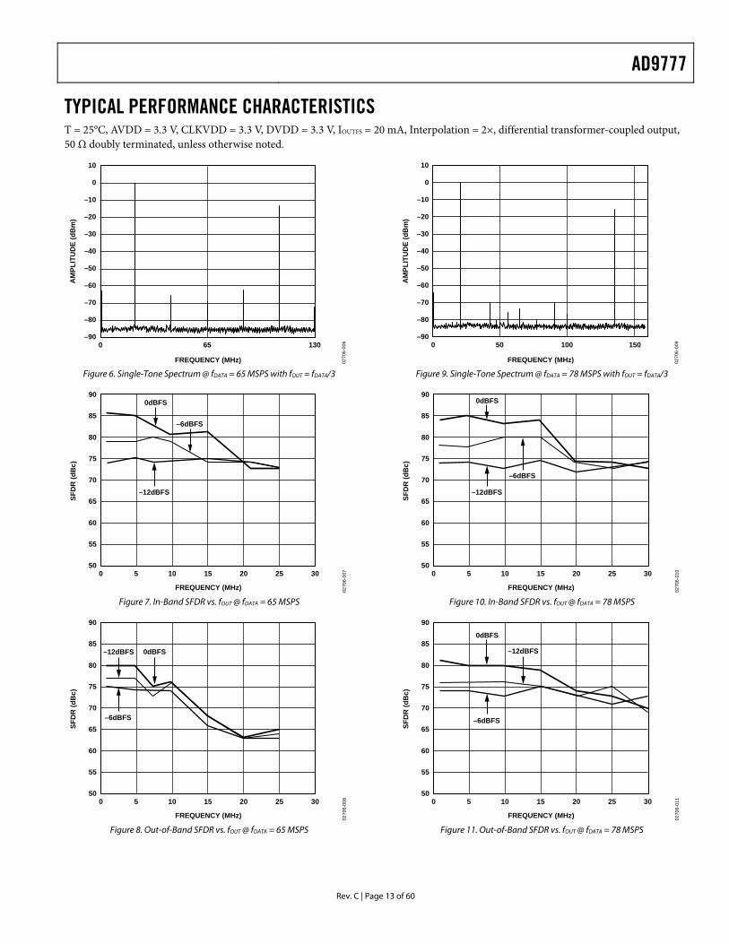
TYPICAL PERFORMANCE CHARACTERISTICS T = 25°C, AVDD = 3.3 V, CLKVDD = 3.3 V, DVDD = 3.3 V, IOUTFS = 20 mA, Interpolation = 2×, differential transformer-coupled output, 50 Ω doubly terminated, unless otherwise noted.
–90
–80
–70
–60
–50
–40
–30
–20
–10
0
10
AM
PLIT
UD
E (d
Bm
)
FREQUENCY (MHz)
0 65 13002
706-
006
Figure 6. Single-Tone Spectrum @ fDATA = 65 MSPS with fOUT = fDATA/3
50
55
60
65
70
75
SFD
R (d
Bc)
80
85
90
10 150 5 20 25 30
FREQUENCY (MHz)
0dBFS
–6dBFS
–12dBFS
0270
6-00
7
Figure 7. In-Band SFDR vs. fOUT @ fDATA = 65 MSPS
50
55
60
65
70
75
SFD
R (d
Bc)
80
85
90
10 150 5 20 25 30
FREQUENCY (MHz)
0dBFS
–6dBFS
–12dBFS
0270
6-00
8
Figure 8. Out-of-Band SFDR vs. fOUT @ fDATA = 65 MSPS
–90
–80
–70
–60
–50
–40
–30
–20
–10
0
10
AM
PLIT
UD
E (d
Bm
)
FREQUENCY (MHz)
0 10050 150
0270
6-00
9
Figure 9. Single-Tone Spectrum @ fDATA = 78 MSPS with fOUT = fDATA/3
50
55
60
65
70
75
SFD
R (d
Bc)
80
85
90
10 150 5 20 25 30
FREQUENCY (MHz)
0dBFS
–6dBFS
–12dBFS
0270
6-01
0
Figure 10. In-Band SFDR vs. fOUT @ fDATA = 78 MSPS
50
55
60
65
70
75
SFD
R (d
Bc)
80
85
90
10 150 5 20 25 30
FREQUENCY (MHz)
0dBFS
–6dBFS
–12dBFS
0270
6-01
1
Figure 11. Out-of-Band SFDR vs. fOUT @ fDATA = 78 MSPS
AD9777
Rev. C | Page 14 of 60
–90
–80
–70
–60
–50
–40
–30
–20
–10
0
10
AM
PLIT
UD
E (d
Bm
)
FREQUENCY (MHz)
0 200100 300
0270
6-01
2
Figure 12. Single-Tone Spectrum @ fDATA = 160 MSPS with fOUT = fDATA/3
50
55
60
65
70
75
SFD
R (d
Bc)
80
85
90
0 10 20 30 40 50
FREQUENCY (MHz)
0dBFS
–12dBFS–6dBFS
0270
6-01
3
Figure 13. In-Band SFDR vs. fOUT @ fDATA = 160 MSPS
50
55
60
65
70
75
SFD
R (d
Bc)
80
85
90
0 10 20 30 40 50
FREQUENCY (MHz)
0dBFS
–6dBFS –12dBFS
0270
6-01
4
Figure 14. Out-of-Band SFDR vs. fOUT @ fDATA = 160 MSPS
50
55
60
65
70
75
IMD
(dB
c)
80
85
90
10 150 5 20 25 30
FREQUENCY (MHz)
0dBFS
–6dBFS
–3dBFS
0270
6-01
5
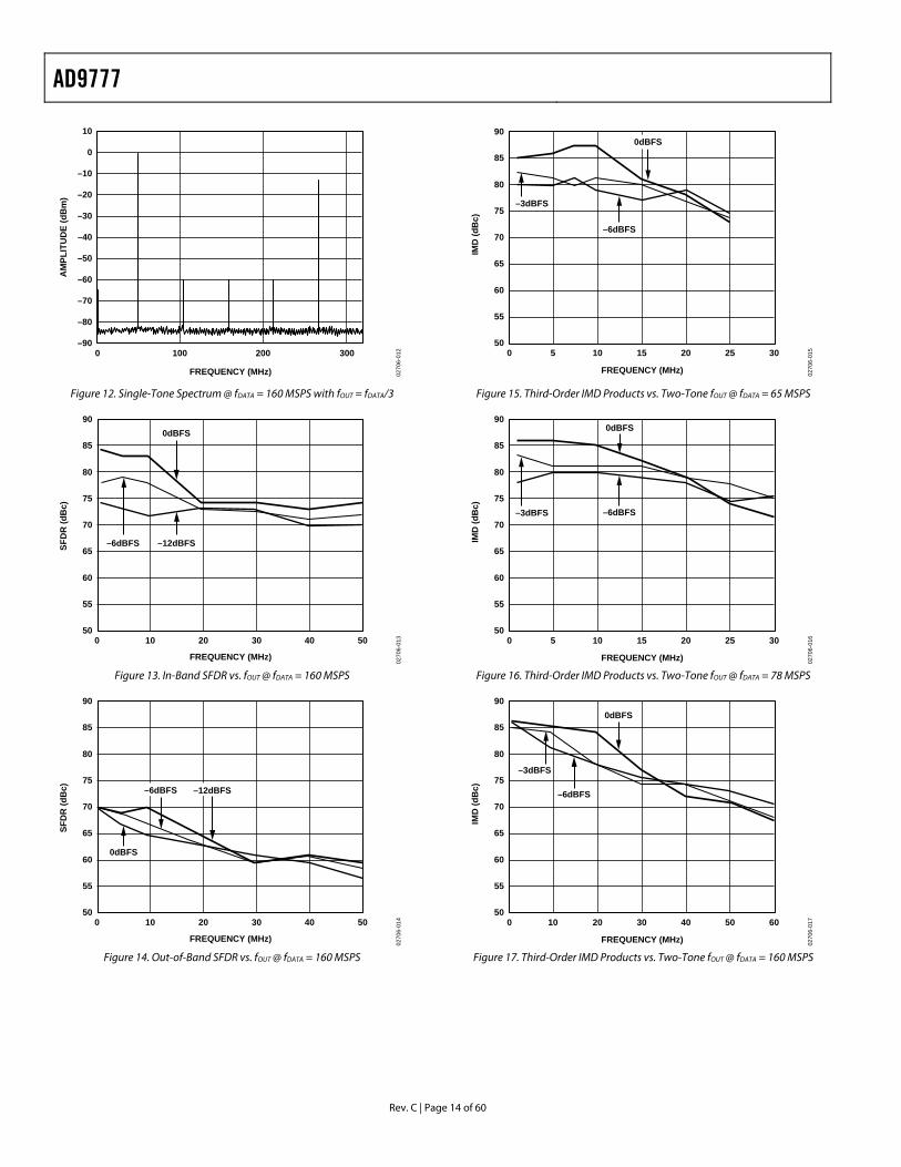
Figure 15. Third-Order IMD Products vs. Two-Tone fOUT @ fDATA = 65 MSPS
50
55
60
65
70
75
IMD
(dB
c)80
85
90
10 150 5 20 25 30
FREQUENCY (MHz)
0dBFS
–6dBFS–3dBFS
0270
6-01
6
Figure 16. Third-Order IMD Products vs. Two-Tone fOUT @ fDATA = 78 MSPS
50
55
60
65
70
75
IMD
(dB
c)
80
85
90
20 300 10 40 50 60
FREQUENCY (MHz)
0dBFS
–6dBFS
–3dBFS
0270
6-01
7
Figure 17. Third-Order IMD Products vs. Two-Tone fOUT @ fDATA = 160 MSPS
AD9777
Rev. C | Page 15 of 60
50
55
60
65
70
75
IMD
(dB
c)
80
85
90
20 300 10 40 50 60
FREQUENCY (MHz)
4×
8×
1×
2×
0270
6-01
8
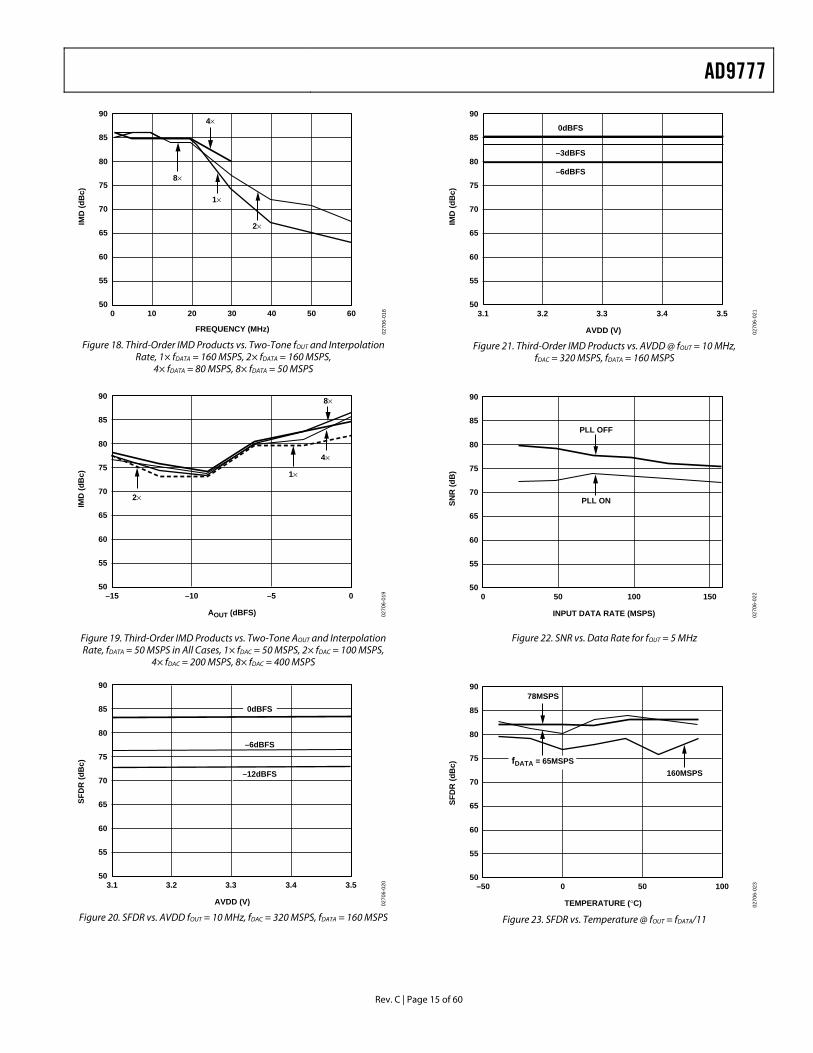
Figure 18. Third-Order IMD Products vs. Two-Tone fOUT and Interpolation
Rate, 1× fDATA = 160 MSPS, 2× fDATA = 160 MSPS, 4× fDATA = 80 MSPS, 8× fDATA = 50 MSPS
50
55
60
65
70
75
IMD
(dB
c)
80
85
90
AOUT (dBFS)
–15 –5–10 0
8×
2×
1×
4×
0270
6-01
9
Figure 19. Third-Order IMD Products vs. Two-Tone AOUT and Interpolation Rate, fDATA = 50 MSPS in All Cases, 1× fDAC = 50 MSPS, 2× fDAC = 100 MSPS,
4× fDAC = 200 MSPS, 8× fDAC = 400 MSPS
50
55
60
65
70
75
SFD
R (d
Bc)
80
85
90
AVDD (V)
3.23.1 3.3 3.4 3.5
0dBFS
–6dBFS
–12dBFS
0270
6-02
0
Figure 20. SFDR vs. AVDD fOUT = 10 MHz, fDAC = 320 MSPS, fDATA = 160 MSPS
50
55
60
65
70
75
IMD
(dB
c)
80
85
90
AVDD (V)
3.23.1 3.3 3.4 3.5
0dBFS
–6dBFS
–3dBFS
0270
6-02
1
Figure 21. Third-Order IMD Products vs. AVDD @ fOUT = 10 MHz,
fDAC = 320 MSPS, fDATA = 160 MSPS
50
55
60
65
70
75
SNR
(dB
)80
85
90
INPUT DATA RATE (MSPS)
0 10050 150
PLL OFF
PLL ON
0270
6-02
2
Figure 22. SNR vs. Data Rate for fOUT = 5 MHz
50
55
60
65
70
75
SFD
R (d
Bc)
80
85
90
TEMPERATURE (°C)
–50 500 100
78MSPS
160MSPSfDATA = 65MSPS
0270
6-02
3
Figure 23. SFDR vs. Temperature @ fOUT = fDATA/11
AD9777
Rev. C | Page 16 of 60
–100
–90
–80
–70
–60
–50
–40
–30
–20
–10
0
AM
PLIT
UD
E (d
Bm
)
FREQUENCY (MHz)
0 10050 150
0270
6-02
4
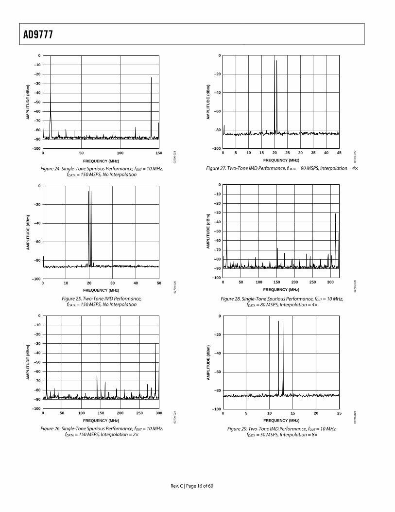
Figure 24. Single-Tone Spurious Performance, fOUT = 10 MHz,
fDATA = 150 MSPS, No Interpolation
–100
–80
–60
–40
–20
0
AM
PLIT
UD
E (d
Bm
)
0 10 20 30 40 50
FREQUENCY (MHz)
0270
6-02
5
Figure 25. Two-Tone IMD Performance,
fDATA = 150 MSPS, No Interpolation
–100
–90
–80
–70
–60
–50
–40
–30
–20
–10
0
AM
PLIT
UD
E (d
Bm
)
100 1500 50 200 250 300
FREQUENCY (MHz) 0270
6-02
6
Figure 26. Single-Tone Spurious Performance, fOUT = 10 MHz,
fDATA = 150 MSPS, Interpolation = 2×
–100
–80
–60
–40
–20
0
AM
PLIT
UD
E (d
Bm
)
0 5 10 15 20 25 30 35 40 45
FREQUENCY (MHz) 0270
6-02
7
Figure 27. Two-Tone IMD Performance, fDATA = 90 MSPS, Interpolation = 4×
–100
–90
–80
–70
–60
–50
–40
–30
–20
–10
0
AM
PLIT
UD
E (d
Bm
)
100 1500 50 200 250 300
FREQUENCY (MHz) 0270
6-02
8
Figure 28. Single-Tone Spurious Performance, fOUT = 10 MHz, fDATA = 80 MSPS, Interpolation = 4×
–100
–80
–60
–40
–20
0
AM
PLIT
UD
E (d
Bm
)
0 5 10 15 20 25
FREQUENCY (MHz)
0270
6-02
9
Figure 29. Two-Tone IMD Performance, fOUT = 10 MHz,
fDATA = 50 MSPS, Interpolation = 8×
AD9777
Rev. C | Page 17 of 60
–100
–90
–80
–70
–60
–50
–40
–30
–20
–10
0
AM
PLIT
UD
E (d
Bm
)
FREQUENCY (MHz)
1000 200 300 400
0270
6-03
0
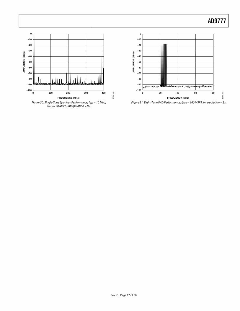
Figure 30. Single-Tone Spurious Performance, fOUT = 10 MHz,
fDATA = 50 MSPS, Interpolation = 8×
–100
–90
–80
–70
–60
–50
–40
–30
–20
–10
0
AM
PLIT
UD
E (d
Bm
)
FREQUENCY (MHz)
200 40 60
0270
6-03
180
Figure 31. Eight-Tone IMD Performance, fDATA = 160 MSPS, Interpolation = 8x
AD9777
Rev. C | Page 18 of 60
MODE CONTROL (VIA SPI PORT)
Table 9. Mode Control via SPI Port1 Address Bit 7 Bit 6 Bit 5 Bit 4 Bit 3 Bit 2 Bit 1 Bit 0 00h SDIO
Bidirectional 0 = Input 1 = I/O
LSB, MSB First 0 = MSB 1 = LSB
Software Reset on Logic 1
Sleep Mode Logic 1 Shuts Down the DAC Output Currents
Power-Down Mode Logic 1 Shuts Down All Digital and Analog Functions
1R/2R Mode DAC Output Current Set by One or Two External Resistors 0 = 2R, 1 = 1R
PLL_LOCK Indicator
01h Filter Interpolation Rate (1×, 2×, 4×, 8×)
Filter Interpolation Rate (1×, 2×, 4×, 8×)
ModulationMode (None, fS/2, fS/4, fS/8)
Modulation Mode (None, fS/2, fS/4, fS/8)
0 = No Zero Stuffing on Interpolation Filters, Logic 1 Enables Zero Stuffing
1 = Real Mix Mode 0 = Complex Mix Mode
0 = e−jωt 1 = e+jωt
DATACLK/ PLL_LOCK2
Select 0 = PLL_LOCK 1 = DATACLK
02h 0 = Signed Input Data 1 = Unsigned
0 = Two-Port Mode 1 = One-Port Mode
DATACLK Driver Strength
DATACLK Invert 0 = No Invert 1 = Invert
ONEPORTCLK Invert 0 = No Invert 1 = Invert
IQSEL Invert 0 = No Invert 1 = Invert
Q First 0 = I First 1 = Q First
03h Data Rate2 Clock Output
PLL Divide (Prescaler) Ratio
PLL Divide (Prescaler) Ratio
04h 0 = PLL OFF2 1 = PLL ON
0 = Automatic Charge Pump Control 1 = Programmable
PLL Charge Pump Control
PLL Charge Pump Control
PLL Charge Pump Control
05h IDAC Fine Gain Adjustment
IDAC Fine Gain Adjustment
IDAC Fine Gain Adjustment
IDAC Fine Gain Adjustment
IDAC Fine Gain Adjustment
IDAC Fine Gain Adjustment
IDAC Fine Gain Adjustment
IDAC Fine Gain Adjustment
06h IDAC Coarse Gain Adjustment
IDAC Coarse Gain Adjustment
IDAC Coarse GainAdjustment
IDAC Coarse GainAdjustment
07h IDAC Offset Adjustment Bit 9
IDAC Offset Adjustment Bit 8
IDAC OffsetAdjustment Bit 7
IDAC Offset Adjustment Bit 6
IDAC Offset Adjustment Bit 5
IDAC Offset Adjustment Bit 4
IDAC OffsetAdjustmentBit 3
IDAC OffsetAdjustmentBit 2
08h IDAC IOFFSET Direction 0 = IOFFSET on IOUTA
1 = IOFFSET on IOUTB
IDAC OffsetAdjustmentBit 1
IDAC OffsetAdjustmentBit 0
09h QDAC Fine Gain Adjustment
QDAC Fine Gain Adjustment
QDAC Fine Gain Adjustment
QDAC Fine Gain Adjustment
QDAC Fine Gain Adjustment
QDAC Fine Gain Adjustment
QDAC Fine Gain Adjustment
QDAC Fine Gain Adjustment
AD9777
Rev. C | Page 19 of 60
Address Bit 7 Bit 6 Bit 5 Bit 4 Bit 3 Bit 2 Bit 1 Bit 0 0Ah QDAC
Coarse Gain Adjustment
QDAC Coarse Gain Adjustment
QDAC Coarse GainAdjustment
QDAC Coarse GainAdjustment
0Bh QDAC Offset Adjustment Bit 9
QDAC Offset Adjustment Bit 8
QDAC Offset Adjustment Bit 7
QDAC OffsetAdjustment Bit 6
QDAC Offset Adjustment Bit 5
QDAC Offset Adjustment Bit 4
QDAC Offset AdjustmentBit 3
QDAC Offset AdjustmentBit 2
0Ch QDAC IOFFSET Direction 0 = IOFFSET on IOUTA 1 = IOFFSET on IOUTB
QDAC Offset AdjustmentBit 1
QDAC Offset AdjustmentBit 0
0Dh Version Register
Version Register
Version Register
Version Register
1 Default values are shown in bold. 2 For more information, see the Two Port Data Input Mode section.
AD9777
Rev. C | Page 20 of 60
REGISTER DESCRIPTION Address 00h
Bit 7: Logic 0 (default) causes the SPI_SDIO pin to act as an input during the data transfer (Phase 2) of the communications cycle. When set to 1, SPI_SDIO can act as an input or output, depending on Bit 7 of the instruction byte.
Bit 6: Logic 0 (default). Determines the direction (LSB/MSB first) of the communications and data transfer communications cycles. Refer to the MSB/LSB Transfers section for more details.
Bit 5: Writing a 1 to this bit resets the registers to their default values and restarts the chip. The RESET bit always reads back 0. Register Address 00h bits are not cleared by this software reset. However, a high level at the RESET pin forces all registers, including those in Address 00h, to their default state.
Bit 4: Sleep Mode. A Logic 1 to this bit shuts down the DAC output currents.
Bit 3: Power-Down. Logic 1 shuts down all analog and digital functions except for the SPI port.
Bit 2: 1R/2R Mode. The default (0) places the AD9777 in two resistor mode. In this mode, the IREF currents for the I and Q DAC references are set separately by the RSET resistors on FSADJ2 and FSADJ1 (Pins 59 and 60). In 2R mode, assuming the coarse gain setting is full scale and the fine gain setting is 0, IFULLSCALE1 = 32 × VREF/FSADJ1 and IFULLSCALE2 = 32 × VREF/FSADJ2. With this bit set to 1, the reference currents for both I and Q DACs are controlled by a single resistor on Pin 60. IFULLSCALE in one resistor mode for both the I and Q DACs is half of what it would be in 2R mode, assuming all other conditions (RSET, register settings) remain unchanged. The full-scale current of each DAC can still be set to 20 mA by choosing a resistor of half the value of the RSET value used in 2R mode.
Bit 1: PLL_LOCK Indicator. When the PLL is enabled, reading this bit gives the status of the PLL. A Logic 1 indicates the PLL is locked. A Logic 0 indicates an unlocked state.
Address 01h
Bit 7, Bit 6: This is the filter interpolation rate according to the following table. 00 1× 01 2× 10 4× 11 8× Bit 5 and Bit 4: This is the modulation mode according to the following table. 00 none 01 fS/2 10 fS/4 11 fS/8
Bit 3: Logic 1 enables zero stuffing mode for interpolation filters.
Bit 2: Default (1) enables the real mix mode. The I and Q data channels are individually modulated by fS/2, fS/4, or fS/8 after the interpolation filters. However, no complex modulation is done. In the complex mix mode (Logic 0), the digital modulators on the I and Q data channels are coupled to create a digital complex modulator. When the AD9777 is applied in conjunction with an external quadrature modulator, rejection can be achieved of either the higher or lower frequency image around the second IF frequency (that is, the LO of the analog quadrature modulator external to the AD9777) according to the bit value of Register 01h, Bit 1.
Bit 1: Logic 0 (default) causes the complex modulation to be of the form e−jωt, resulting in the rejection of the higher frequency image when the AD9777 is used with an external quadrature modulator. A Logic 1 causes the modulation to be of the form e+jωt, which causes rejection of the lower frequency image.
Bit 0: In two-port mode, a Logic 0 (default) causes Pin 8 to act as a lock indicator for the internal PLL. A Logic 1 in this register causes Pin 8 to act as a DATACLK. For more information, see the Two Port Data Input Mode section.
Address 02h
Bit 7: Logic 0 (default) causes data to be accepted on the inputs as twos complement binary. Logic 1 causes data to be accepted as straight binary.
Bit 6: Logic 0 (default) places the AD9777 in two-port mode. I and Q data enters the AD9777 via Ports 1 and 2, respectively. A Logic 1 places the AD9777 in one-port mode in which interleaved I and Q data is applied to Port 1. See Table 8 for detailed information on how to use the DATACLK/PLL_LOCK, IQSEL, and ONEPORTCLK modes.
Bit 5: DATACLK Driver Strength. With the internal PLL disabled and this bit set to Logic 0, it is recommended that DATACLK be buffered. When this bit is set to Logic 1, DATACLK acts as a stronger driver capable of driving small capacitive loads.
Bit 4: Logic 0 (default). A value of 1 inverts DATACLK at Pin 8.
Bit 2: Logic 0 (default). A value of 1 inverts ONEPORTCLK at Pin 32.
Bit 1: Logic 0 (default) causes IQSEL = 0 to direct input data to the I channel, while IQSEL = 1 directs input data to the Q channel.
Bit 0: Logic 0 (default) defines IQ pairing as IQ, IQ…, while programming a Logic 1 causes the pair ordering to be QI, QI…
AD9777
Rev. C | Page 21 of 60
Address 03h
Bit 7: This allows the data rate clock (divided down from the DAC clock) to be output at either the DATACLK/PLL_LOCK pin (Pin 8) or at the SPI_SDO pin (Pin 53). The default of 0 in this register enables the data rate clock at DATACLK/ PLL_LOCK, while a 1 in this register causes the data rate clock to be output at SPI_SDO. For more information, see the Two Port Data Input Mode section.
Bit 1, Bit 0: Setting this divide ratio to a higher number allows the VCO in the PLL to run at a high rate (for best performance) while the DAC input and output clocks run substantially slower. The divider ratio is set according to the following table.
00 ÷1
01 ÷2
10 ÷4
11 ÷8
Address 04h
Bit 7: Logic 0 (default) disables the internal PLL. Logic 1 enables the PLL.
Bit 6: Logic 0 (default) sets the charge pump control to automatic. In this mode, the charge pump bias current is controlled by the divider ratio defined in Address 03h, Bits 1 and 0. Logic 1 allows the user to manually define the charge pump bias current using Address 04h, Bits 2, 1, and 0. Adjusting the charge pump bias current allows the user to optimize the noise/settling performance of the PLL.
Bit 2, Bit 1, Bit 0: With the charge pump control set to manual, these bits define the charge pump bias current according to the following table.
000 50 µA
001 100 µA
010 200 µA
011 400 µA
111 800 µA
Address 05h, 09h
Bit 7, Bit 6, Bit 5, Bit 4, Bit 3, Bit 2, Bit 1, and Bit 0: These bits represent an 8-bit binary number (Bit 7 MSB) that defines the fine gain adjustment of the I (05h) and Q (09h) DAC according to Equation 1.
Address 06h, 0Ah
Bit 3, Bit 2, Bit 1, and Bit 0: These bits represent a 4-bit binary number (Bit 3 MSB) that defines the coarse gain adjustment of the I (06h) and Q (0Ah) DACs according to Equation 1.
Address 07h, 0Bh
Bit 7, Bit 6, Bit 5, Bit 4, Bit 3, Bit 2, Bit 1, and Bit 0: These bits are used in conjunction with Address 08h, 0Ch, Bits 1, 0.
Address 08h, 0Ch
Bit 1 and Bit 0: The 10 bits from these two address pairs (07h, 08h and 0Bh, 0Ch) represent a 10-bit binary number that defines the offset adjustment of the I and Q DACs according to Equation 1. (07h, 0Bh–Bit 7 MSB/08h, 0Ch–Bit 0 LSB).
Address 08h, 0Ch
Bit 7: This bit determines the direction of the offset of the I (08h) and Q (0Ch) DACs. A Logic 0 applies a positive offset current to IOUTA, while a Logic 1 applies a positive offset current to IOUTB. The magnitude of the offset current is defined by the bits in Addresses 07h, 0Bh, 08h, 0Ch according to Equation 1. Equation 1 shows IOUTA and IOUTB as a function of fine gain, coarse gain, and offset adjustment when using 2R mode. In 1R mode, the current IREF is created by a single FSADJ resistor (Pin 60). This current is divided equally into each channel so that a scaling factor of one-half must be added to these equations for full-scale currents for both DACs and the offset.
)(1024
4
)(2
1224
102425632
316
18
6
)(224
102425632
316
18
6
16
16
16
AOFFSET
II
ADATAFINEICOARSEI
I
ADATAFINEICOARSEI
I
REFOFFSET
REFREFOUTB
REFREFOUTA
⎟⎠⎞
⎜⎝⎛×=
⎥⎥⎦
⎤
⎢⎢⎣
⎡⎟⎟⎠
⎞⎜⎜⎝
⎛ −−⎟⎠⎞
⎜⎝⎛×⎥
⎦
⎤⎢⎣
⎡⎟⎠⎞
⎜⎝⎛⎟⎠⎞
⎜⎝⎛ ×
−⎟⎠⎞
⎜⎝⎛ +⎟⎠⎞
⎜⎝⎛ ×
=
⎥⎦
⎤⎢⎣
⎡⎟⎠⎞
⎜⎝⎛⎟⎠⎞
⎜⎝⎛×⎥
⎦
⎤⎢⎣
⎡⎟⎠⎞
⎜⎝⎛⎟⎠⎞
⎜⎝⎛ ×
−⎟⎠⎞
⎜⎝⎛ +⎟⎠⎞
⎜⎝⎛ ×
=
(1)
AD9777
Rev. C | Page 22 of 60
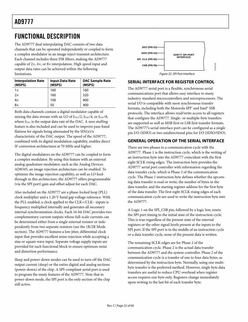
FUNCTIONAL DESCRIPTIONThe AD9777 dual interpolating DAC consists of two data channels that can be operated independently or coupled to form a complex modulator in an image reject transmit architecture. Each channel includes three FIR filters, making the AD9777 capable of 2×, 4×, or 8× interpolation. High speed input and output data rates can be achieved within the following limitations.
Interpolation Rate (MSPS)
Input Data Rate (MSPS)
DAC Sample Rate (MSPS)
1× 160 160 2× 160 320 4× 100 400 8× 50 400
Both data channels contain a digital modulator capable of mixing the data stream with an LO of fDAC/2, fDAC/4, or fDAC/8, where fDAC is the output data rate of the DAC. A zero stuffing feature is also included and can be used to improve pass-band flatness for signals being attenuated by the SIN(x)/x characteristic of the DAC output. The speed of the AD9777, combined with its digital modulation capability, enables direct IF conversion architectures at 70 MHz and higher.
The digital modulators on the AD9777 can be coupled to form a complex modulator. By using this feature with an external analog quadrature modulator, such as the Analog Devices AD8345, an image rejection architecture can be enabled. To optimize the image rejection capability, as well as LO feed-through in this architecture, the AD9777 offers programmable (via the SPI port) gain and offset adjust for each DAC.
Also included on the AD9777 are a phase-locked loop (PLL) clock multiplier and a 1.20 V band gap voltage reference. With the PLL enabled, a clock applied to the CLK+/CLK− inputs is frequency multiplied internally and generates all necessary internal synchronization clocks. Each 16-bit DAC provides two complementary current outputs whose full-scale currents can be determined either from a single external resistor or inde-pendently from two separate resistors (see the 1R/2R Mode section). The AD9777 features a low jitter, differential clock input that provides excellent noise rejection while accepting a sine or square wave input. Separate voltage supply inputs are provided for each functional block to ensure optimum noise and distortion performance.
Sleep and power-down modes can be used to turn off the DAC output current (sleep) or the entire digital and analog sections (power-down) of the chip. A SPI-compliant serial port is used to program the many features of the AD9777. Note that in power-down mode, the SPI port is the only section of the chip still active.
SDO (PIN 53)
SDIO (PIN 54)
SPI_CLK (PIN 55)
CSB (PIN 56)
AD9777 SPI PORTINTERFACE
0270
6-03
2
Figure 32. SPI Port Interface
SERIAL INTERFACE FOR REGISTER CONTROL The AD9777 serial port is a flexible, synchronous serial communications port that allows easy interface to many industry-standard microcontrollers and microprocessors. The serial I/O is compatible with most synchronous transfer formats, including both the Motorola SPI® and Intel® SSR protocols. The interface allows read/write access to all registers that configure the AD9777. Single- or multiple-byte transfers are supported as well as MSB first or LSB first transfer formats. The AD9777’s serial interface port can be configured as a single pin I/O (SDIO) or two unidirectional pins for I/O (SDIO/SDO).
GENERAL OPERATION OF THE SERIAL INTERFACE There are two phases to a communication cycle with the AD9777. Phase 1 is the instruction cycle, which is the writing of an instruction byte into the AD9777 coincident with the first eight SCLK rising edges. The instruction byte provides the AD9777 serial port controller with information regarding the data transfer cycle, which is Phase 2 of the communication cycle. The Phase 1 instruction byte defines whether the upcom-ing data transfer is read or write, the number of bytes in the data transfer, and the starting register address for the first byte of the data transfer. The first eight SCLK rising edges of each communication cycle are used to write the instruction byte into the AD9777.
A Logic 1 on the SPI_CSB pin, followed by a logic low, resets the SPI port timing to the initial state of the instruction cycle. This is true regardless of the present state of the internal registers or the other signal levels present at the inputs to the SPI port. If the SPI port is in the middle of an instruction cycle or a data transfer cycle, none of the present data is written.
The remaining SCLK edges are for Phase 2 of the communication cycle. Phase 2 is the actual data transfer between the AD9777 and the system controller. Phase 2 of the communication cycle is a transfer of one to four data bytes, as determined by the instruction byte. Normally, using one multi-byte transfer is the preferred method. However, single byte data transfers are useful to reduce CPU overhead when register access requires one byte only. Registers change immediately upon writing to the last bit of each transfer byte.
AD9777
Rev. C | Page 23 of 60
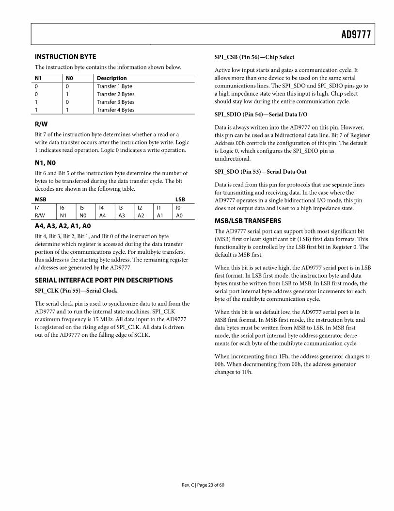
INSTRUCTION BYTE The instruction byte contains the information shown below.
N1 N0 Description 0 0 Transfer 1 Byte 0 1 Transfer 2 Bytes 1 0 Transfer 3 Bytes 1 1 Transfer 4 Bytes
R/W Bit 7 of the instruction byte determines whether a read or a write data transfer occurs after the instruction byte write. Logic 1 indicates read operation. Logic 0 indicates a write operation.
N1, N0 Bit 6 and Bit 5 of the instruction byte determine the number of bytes to be transferred during the data transfer cycle. The bit decodes are shown in the following table.
MSB LSB I7 I6 I5 I4 I3 I2 I1 I0 R/W N1 N0 A4 A3 A2 A1 A0
A4, A3, A2, A1, A0 Bit 4, Bit 3, Bit 2, Bit 1, and Bit 0 of the instruction byte determine which register is accessed during the data transfer portion of the communications cycle. For multibyte transfers, this address is the starting byte address. The remaining register addresses are generated by the AD9777.
SERIAL INTERFACE PORT PIN DESCRIPTIONS SPI_CLK (Pin 55)—Serial Clock
The serial clock pin is used to synchronize data to and from the AD9777 and to run the internal state machines. SPI_CLK maximum frequency is 15 MHz. All data input to the AD9777 is registered on the rising edge of SPI_CLK. All data is driven out of the AD9777 on the falling edge of SCLK.
SPI_CSB (Pin 56)—Chip Select
Active low input starts and gates a communication cycle. It allows more than one device to be used on the same serial communications lines. The SPI_SDO and SPI_SDIO pins go to a high impedance state when this input is high. Chip select should stay low during the entire communication cycle.
SPI_SDIO (Pin 54)—Serial Data I/O
Data is always written into the AD9777 on this pin. However, this pin can be used as a bidirectional data line. Bit 7 of Register Address 00h controls the configuration of this pin. The default is Logic 0, which configures the SPI_SDIO pin as unidirectional.
SPI_SDO (Pin 53)—Serial Data Out
Data is read from this pin for protocols that use separate lines for transmitting and receiving data. In the case where the AD9777 operates in a single bidirectional I/O mode, this pin does not output data and is set to a high impedance state.
MSB/LSB TRANSFERS The AD9777 serial port can support both most significant bit (MSB) first or least significant bit (LSB) first data formats. This functionality is controlled by the LSB first bit in Register 0. The default is MSB first.
When this bit is set active high, the AD9777 serial port is in LSB first format. In LSB first mode, the instruction byte and data bytes must be written from LSB to MSB. In LSB first mode, the serial port internal byte address generator increments for each byte of the multibyte communication cycle.
When this bit is set default low, the AD9777 serial port is in MSB first format. In MSB first mode, the instruction byte and data bytes must be written from MSB to LSB. In MSB first mode, the serial port internal byte address generator decre-ments for each byte of the multibyte communication cycle.
When incrementing from 1Fh, the address generator changes to 00h. When decrementing from 00h, the address generator changes to 1Fh.
AD9777
Rev. C | Page 24 of 60
INSTRUCTION CYCLE DATA TRANSFER CYCLE
CS
SCLK
SDIO
SDO
R/W I4 I3 I2 I1 I0 D7N D6N
D7N D6N
D20 D10 D00
D20 D10 D00
I6(N) I5(N)
0270
6-03
3
Figure 33. Serial Register Interface Timing MSB First
CS
SCLK
SDIO
SDO
INSTRUCTION CYCLE DATA TRANSFER CYCLE
I0 I1 I2 I3 I4 I5(N) I6(N) R/W D00 D10 D20 D6N D7N
D00 D10 D20 D6N D7N 0270
6-03
4
Figure 34. Serial Register Interface Timing LSB First
T
CS
SCLK
SDIO
tDS tSCLK
tPWH
tDS tDH
tPWL
INSTRUCTION BIT 7 INSTRUCTION BIT 6
0270
6-03
5
Figure 35. Timing Diagram for Register Write to AD9777
CS
SCLK
SDIO
SDODATA BIT N
tDV
DATA BIT N–1
0270
6-03
6
Figure 36. Timing Diagram for Register Read from AD9777
AD9777
Rev. C | Page 25 of 60
NOTES ON SERIAL PORT OPERATION The AD9777 serial port configuration bits reside in Bit 6 and Bit 7 of Register Address 00h. It is important to note that the configuration changes immediately upon writing to the last bit of the register. For multibyte transfers, writing to this register may occur during the middle of the communication cycle. Care must be taken to compensate for this new configuration for the remaining bytes of the current communication cycle.
The same considerations apply to setting the reset bit in Register Address 00h. All other registers are set to their default values, but the software reset does not affect the bits in Register Address 00h.
It is recommended to use only single byte transfers when changing serial port configurations or initiating a software reset.
A write to Bit 1, Bit 2, and Bit 3 of Address 00h with the same logic levels as for Bit 7, Bit 6, and Bit 5 (bit pattern: XY1001YX binary) allows the user to reprogram a lost serial port configu-ration and to reset the registers to their default values. A second write to Address 00h with reset bit low and serial port configu-ration as specified above (XY) reprograms the OSC IN multiplier setting. A changed fSYSCLK frequency is stable after a maximum of 200 fMCLK cycles (equals wake-up time).
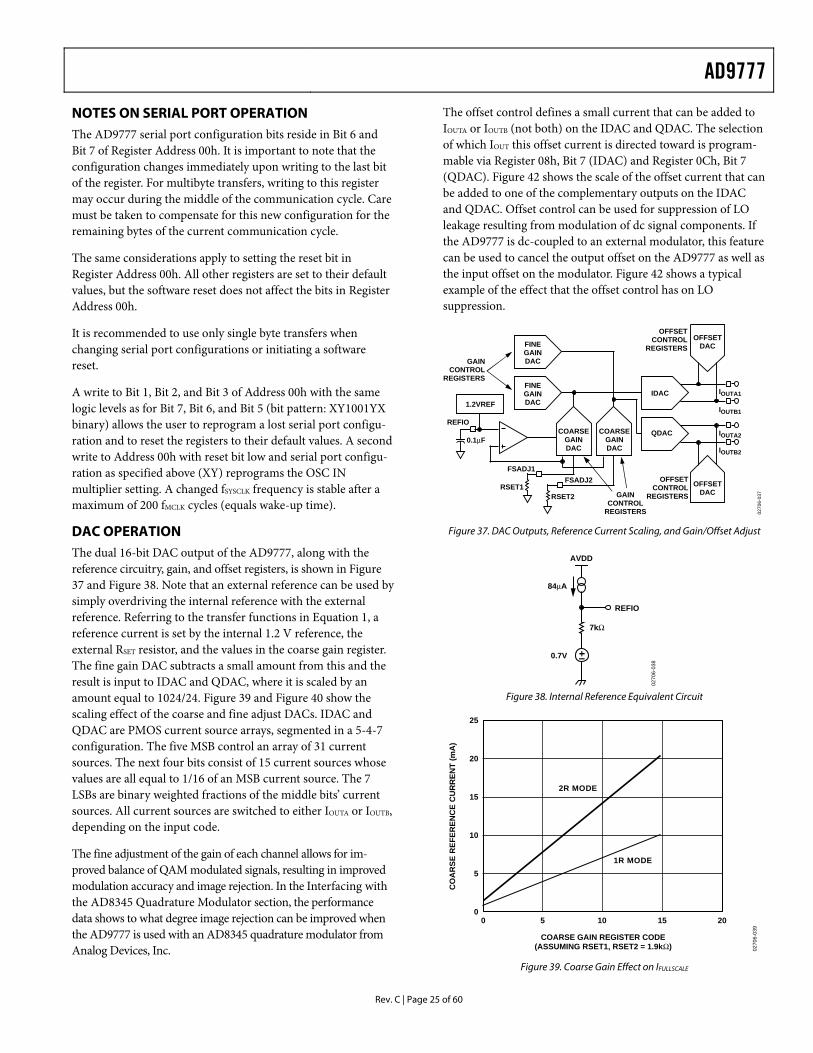
DAC OPERATION The dual 16-bit DAC output of the AD9777, along with the reference circuitry, gain, and offset registers, is shown in Figure 37 and Figure 38. Note that an external reference can be used by simply overdriving the internal reference with the external reference. Referring to the transfer functions in Equation 1, a reference current is set by the internal 1.2 V reference, the external RSET resistor, and the values in the coarse gain register. The fine gain DAC subtracts a small amount from this and the result is input to IDAC and QDAC, where it is scaled by an amount equal to 1024/24. Figure 39 and Figure 40 show the scaling effect of the coarse and fine adjust DACs. IDAC and QDAC are PMOS current source arrays, segmented in a 5-4-7 configuration. The five MSB control an array of 31 current sources. The next four bits consist of 15 current sources whose values are all equal to 1/16 of an MSB current source. The 7 LSBs are binary weighted fractions of the middle bits’ current sources. All current sources are switched to either IOUTA or IOUTB, depending on the input code.
The fine adjustment of the gain of each channel allows for im-proved balance of QAM modulated signals, resulting in improved modulation accuracy and image rejection. In the Interfacing with the AD8345 Quadrature Modulator section, the performance data shows to what degree image rejection can be improved when the AD9777 is used with an AD8345 quadrature modulator from Analog Devices, Inc.
The offset control defines a small current that can be added to IOUTA or IOUTB (not both) on the IDAC and QDAC. The selection of which IOUT this offset current is directed toward is program-mable via Register 08h, Bit 7 (IDAC) and Register 0Ch, Bit 7 (QDAC). Figure 42 shows the scale of the offset current that can be added to one of the complementary outputs on the IDAC and QDAC. Offset control can be used for suppression of LO leakage resulting from modulation of dc signal components. If the AD9777 is dc-coupled to an external modulator, this feature can be used to cancel the output offset on the AD9777 as well as the input offset on the modulator. Figure 42 shows a typical example of the effect that the offset control has on LO suppression.
FINEGAINDAC
FINEGAINDAC
COARSEGAINDAC
COARSEGAINDAC
OFFSETDAC
OFFSETDACGAIN
CONTROLREGISTERS
OFFSETCONTROL
REGISTERS
GAINCONTROL
REGISTERS
OFFSETCONTROL
REGISTERS
1.2VREFIDAC
QDACREFIO
0.1µF
FSADJ1
RSET1
IOUTA1
IOUTA2
IOUTB1
IOUTB2
RSET2
FSADJ2
0270
6-03
7
Figure 37. DAC Outputs, Reference Current Scaling, and Gain/Offset Adjust
84µA
7kΩ
0.7V
REFIO
AVDD
0270
6-03
8
Figure 38. Internal Reference Equivalent Circuit
2R MODE
1R MODE
0
5
10
15
20
25
CO
AR
SE R
EFER
ENC
E C
UR
REN
T (m
A)
COARSE GAIN REGISTER CODE(ASSUMING RSET1, RSET2 = 1.9kΩ)
50 10 15
0270
6-03
9
20
Figure 39. Coarse Gain Effect on IFULLSCALE
AD9777
Rev. C | Page 26 of 60
–3.0
–2.5
–2.0
–1.5
–1.0
–0.5
0
FIN
E R
EFER
ENC
E C
UR
REN
T (m
A)
0
1R MODE
2R MODE
FINE GAIN REGISTER CODE(ASSUMING RSET1, RSET2 = 1.9kΩ)
200 400 600 800 1000
0270
6-04
0
Figure 40. Fine Gain Effect on IFULLSCALE
In Figure 42, the negative scale represents an offset added to IOUTB, while the positive scale represents an offset added to IOUTA of the respective DAC. Offset Register 1 corresponds to IDAC, while Offset Register 2 corresponds to QDAC. Figure 42 represents the AD9777 synthesizing a complex signal that is then dc-coupled to an AD8345 quadrature modulator with an LO of 800 MHz. The dc coupling allows the input offset of the AD8345 to be calibrated out as well. The LO suppression at the AD8345 output was optimized first by adjusting Offset Register 1 in the AD9777. When an optimal point was found (roughly Code 54), this code was held in Offset Register 1, and Offset Register 2 was adjusted. The resulting LO suppression is 70 dBFS. These are typical numbers, and the specific code for optimization varies from part to part.
0
1
2
3
4
5
OFF
SET
CU
RR
ENT
(mA
)
0
COARSE GAIN REGISTER CODE(ASSUMING RSET1, RSET2 = 1.9kΩ)
2R MODE
1R MODE
0 200 400 600 800 1000
0270
6-04
1
Figure 41. DAC Output Offset Current
–80
–70
–60
–50
–40
–30
LO S
UPP
RES
SIO
N (d
BFS
) –20
–10
0
0–256–768 –512–1024 256 512 768 1024
DAC1, DAC2 (OFFSET REGISTER CODES)
OFFSET REGISTER 1 ADJUSTED
OFFSET REGISTER 2ADJUSTED, WITH OFFSETREGISTER 1 SETTO OPTIMIZED VALUE
0270
6-04
2
Figure 42. Offset Adjust Control, Effect on LO Suppression
1R/2R MODE In 2R mode, the reference current for each channel is set independently by the FSADJ resistor on that channel. The AD9777 can be programmed to derive its reference current from a single resistor on Pin 60 by putting the part into 1R mode. The transfer functions in Equation 1 are valid for 2R mode. In 1R mode, the current developed in the single FSADJ resistor is split equally between the two channels. The result is that in 1R mode, a scale factor of 1/2 must be applied to the formulas in Equation 1. The full-scale DAC current in 1R mode can still be set to as high as 20 mA by using the internal 1.2 V reference and a 950 Ω resistor instead of the 1.9 kΩ resistor typically used in 2R mode.
CLOCK INPUT CONFIGURATION The clock inputs to the AD9777 can be driven differentially or single-ended. The internal clock circuitry has supply and ground (CLKVDD, CLKGND) separate from the other supplies on the chip to minimize jitter from internal noise sources.
Figure 43 shows the AD9777 driven from a single-ended clock source. The CLK+/CLK− pins form a differential input (CLKIN) so that the statically terminated input must be dc-biased to the midswing voltage level of the clock driven input.
AD9777RSERIES
CLK+
CLK–0.1µF
CLKVDD
CLKGND
VTHRESHOLD
0270
6-04
3
Figure 43. Single-Ended Clock Driving Clock Inputs
AD9777
Rev. C | Page 27 of 60
A configuration for differentially driving the clock inputs is given in Figure 44. DC-blocking capacitors can be used to couple a clock driver output whose voltage swings exceed CLKVDD or CLKGND. If the driver voltage swings are within the supply range of the AD9777, the dc-blocking capacitors and bias resistors are not necessary.
AD9777
CLK+0.1µF
0.1µF
0.1µF
1kΩ
1kΩ
1kΩ
1kΩ
ECL/PECL
CLK–
CLKVDD
CLKGND02
706-
044
Figure 44. Differential Clock Driving Clock Inputs
A transformer, such as the T1-1T from Mini-Circuits, can also be used to convert a single-ended clock to differential. This method is used on the AD9777 evaluation board so that an external sine wave with no dc offset can be used as a differential clock.
PECL/ECL drivers require varying termination networks, the details of which are left out of Figure 43 and Figure 44 but can be found in application notes such as AND8020/D from On Semiconductor. These networks depend on the assumed transmission line impedance and power supply voltage of the clock driver. Optimum performance of the AD9777 is achieved when the driver is placed very close to the AD9777 clock inputs, thereby negating any transmission line effects such as reflec-tions due to mismatch.
The quality of the clock and data input signals is important in achieving optimum performance. The external clock driver circuitry should provide the AD9777 with a low jitter clock input that meets the minimum/maximum logic levels while providing fast edges. Although fast clock edges help minimize any jitter that manifests itself as phase noise on a reconstructed waveform, the high gain bandwidth product of the AD9777’s clock input comparator can tolerate differential sine wave inputs as low as 0.5 V p-p with minimal degradation of the output noise floor.
PROGRAMMABLE PLL CLKIN can function either as an input data rate clock (PLL enabled) or as a DAC data rate clock (PLL disabled) according to the state of Address 02h, Bit 7 in the SPI port register. The internal operation of the AD9777 clock circuitry in these two modes is illustrated in Figure 45 and Figure 46.
The PLL clock multiplier and distribution circuitry produce the necessary internal synchronized 1×, 2×, 4×, and 8× clocks for the rising edge triggered latches, interpolation filters, modulators, and DACs. This circuitry consists of a phase detector, charge pump, voltage controlled oscillator (VCO), prescaler, clock distribution, and SPI port control. The charge pump, VCO, differential clock input buffer, phase detector, prescaler, and clock distribution are all powered from CLKVDD. PLL lock status is indicated by the logic signal at the PLL_LOCK pin, as well as by the status of Bit 1, Register 00h. To ensure optimum phase noise performance from the PLL clock multiplier and distribution, CLKVDD should originate from a clean analog supply. Table 10 defines the minimum input data rates versus the interpolation and PLL divider setting. If the input data rate drops below the defined minimum under these conditions, VCO phase noise can increase significantly. The VCO speed is a function of the input data rate, the interpolation rate, and the VCO prescaler, according to the following function:
( )( ) PrescalerRateionInterpolatMHzRateDataInput
MHzSpeedVCO××
=
AD9777
PLLVDD
INPUTDATA
LATCHES
PLL_LOCK1 = LOCK
0 = NO LOCK
SPI PORT
LPF
CLK+ CLK–
INTERPOLATIONFILTERS,
MODULATORS,AND DACS
CLOCKDISTRIBUTION
CIRCUITRY
INTERPOLATIONRATE
CONTROL
INTERNAL SPICONTROL
REGISTERS
MODULATIONRATE
CONTROL
PLLCONTROL(PLL ON)
PLL DIVIDER(PRESCALER)
CONTROL
PRESCALER VCO
PHASEDETECTOR
CHARGEPUMP
21
4 8
0270
6-04
5
Figure 45. PLL and Clock Circuitry with PLL Enabled
AD9777
Rev. C | Page 28 of 60
AD9777
INPUTDATA
LATCHES
PLL_LOCK1 = LOCK
0 = NO LOCK
SPI PORT
CLK+ CLK–
INTERPOLATIONFILTERS,
MODULATORS,AND DACS
CLOCKDISTRIBUTION
CIRCUITRY
INTERPOLATIONRATE
CONTROL
INTERNAL SPICONTROL
REGISTERS
MODULATIONRATE
CONTROL
PLLCONTROL(PLL ON)
PLL DIVIDER(PRESCALER)
CONTROL
PRESCALER VCO
PHASEDETECTOR
CHARGEPUMP
21
4 8
0270
6-04
6
Figure 46. PLL and Clock Circuitry with PLL Disabled
In addition, if the zero stuffing option is enabled, the VCO doubles its speed again. Phase noise can be slightly higher with the PLL enabled. Figure 47 illustrates typical phase noise performance of the AD9777 with 2× interpolation and various input data rates. The signal synthesized for the phase noise measurement was a single carrier at a frequency of fDATA/4. The repetitive nature of this signal eliminates quantization noise and distortion spurs as a factor in the measure-ment. Although the curves blend in Figure 47, the different conditions are given for clarity in the table preceding Figure 47. Figure 47 also contains a table detailing PLL divider settings vs. interpolation rate and maximum and minimum fDATA rates. Note that maximum fDATA rates of 160 MSPS are due to the maximum input data rate of the AD9777. However, maximum rates of less than 160 MSPS and all minimum fDATA rates are due to maximum and mini-mum speeds of the internal PLL VCO. Figure 48 shows typical performance of the PLL lock signal (Pin 8 or Pin 53) when the PLL is in the process of locking.
Table 10. PLL Optimization Interpolation Rate
Divider Setting
Minimum fDATA
Maximum fDATA
1 1 32 160 1 2 16 160 1 4 8 112 1 8 4 56 2 1 24 160 2 2 12 112 2 4 6 56 2 8 3 28 4 1 24 100 4 2 12 56 4 4 6 28 4 8 3 14 8 1 24 50 8 2 12 28 8 4 6 14 8 8 3 7
Table 11. Required PLL Prescaler Ration vs. fDATA fDATA (MSPS) PLL Prescaler Ratio 125 Disabled 125 Enabled Div 1 100 Enabled Div 2 75 Enabled Div 2 50 Enabled Div 4
–110
–100
–80
–40
–20
0
–60
–90
–50
–30
–10
–70
PHA
SE N
OIS
E (d
BFS
)
0 1 2 3 4 5
FREQUENCY OFFSET (MHz)
0270
6-04
7
Figure 47. Phase Noise Performance
0270
6-04
8
Figure 48. PLL_LOCK Output Signal (Pin 8) in the Process of Locking
(Typical Lock Time)
It is important to note that the resistor/capacitor needed for the PLL loop filter is internal on the AD9777. This suffices unless the input data rate is below 10 MHz, in which case an external series RC is required between the LPF and CLKVDD pins.
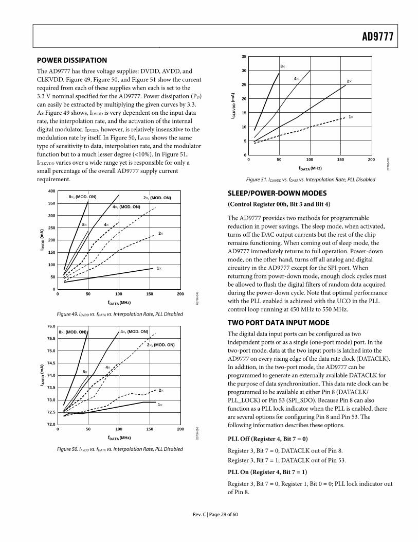
AD9777
Rev. C | Page 29 of 60
POWER DISSIPATION The AD9777 has three voltage supplies: DVDD, AVDD, and CLKVDD. Figure 49, Figure 50, and Figure 51 show the current required from each of these supplies when each is set to the 3.3 V nominal specified for the AD9777. Power dissipation (PD) can easily be extracted by multiplying the given curves by 3.3. As Figure 49 shows, IDVDD is very dependent on the input data rate, the interpolation rate, and the activation of the internal digital modulator. IDVDD, however, is relatively insensitive to the modulation rate by itself. In Figure 50, IAVDD shows the same type of sensitivity to data, interpolation rate, and the modulator function but to a much lesser degree (<10%). In Figure 51, ICLKVDD varies over a wide range yet is responsible for only a small percentage of the overall AD9777 supply current requirement.
8× 4×
2×
1×
0
50
100
150
200
250
I DVD
D (m
A)
300
350
400
fDATA (MHz)
500 100 150 200
8×, (MOD. ON)
4×, (MOD. ON)
2×, (MOD. ON)02
706-
049
Figure 49. IDVDD vs. fDATA vs. Interpolation Rate, PLL Disabled
8×, (MOD. ON)
8×4×
2×
1×
72.0
72.5
73.0
73.5
74.0
74.5
I AVD
D (m
A)
75.0
75.5
76.0
fDATA (MHz)
500 100 150 200
4×, (MOD. ON)
2×, (MOD. ON)
0270
6-05
0
Figure 50. IAVDD vs. fDATA vs. Interpolation Rate, PLL Disabled
8×
4×
1×
2×
0
5
10
15
20
25
30
35
I CLK
VDD
(mA
)
fDATA (MHz)
500 100 150 200
0270
6-05
1
Figure 51. ICLKVDD vs. fDATA vs. Interpolation Rate, PLL Disabled
SLEEP/POWER-DOWN MODES (Control Register 00h, Bit 3 and Bit 4)
The AD9777 provides two methods for programmable reduction in power savings. The sleep mode, when activated, turns off the DAC output currents but the rest of the chip remains functioning. When coming out of sleep mode, the AD9777 immediately returns to full operation. Power-down mode, on the other hand, turns off all analog and digital circuitry in the AD9777 except for the SPI port. When returning from power-down mode, enough clock cycles must be allowed to flush the digital filters of random data acquired during the power-down cycle. Note that optimal performance with the PLL enabled is achieved with the UCO in the PLL control loop running at 450 MHz to 550 MHz.
TWO PORT DATA INPUT MODE The digital data input ports can be configured as two independent ports or as a single (one-port mode) port. In the two-port mode, data at the two input ports is latched into the AD9777 on every rising edge of the data rate clock (DATACLK). In addition, in the two-port mode, the AD9777 can be programmed to generate an externally available DATACLK for the purpose of data synchronization. This data rate clock can be programmed to be available at either Pin 8 (DATACLK/ PLL_LOCK) or Pin 53 (SPI_SDO). Because Pin 8 can also function as a PLL lock indicator when the PLL is enabled, there are several options for configuring Pin 8 and Pin 53. The following information describes these options.
PLL Off (Register 4, Bit 7 = 0)
Register 3, Bit 7 = 0; DATACLK out of Pin 8. Register 3, Bit 7 = 1; DATACLK out of Pin 53.
PLL On (Register 4, Bit 7 = 1)
Register 3, Bit 7 = 0, Register 1, Bit 0 = 0; PLL lock indicator out of Pin 8.
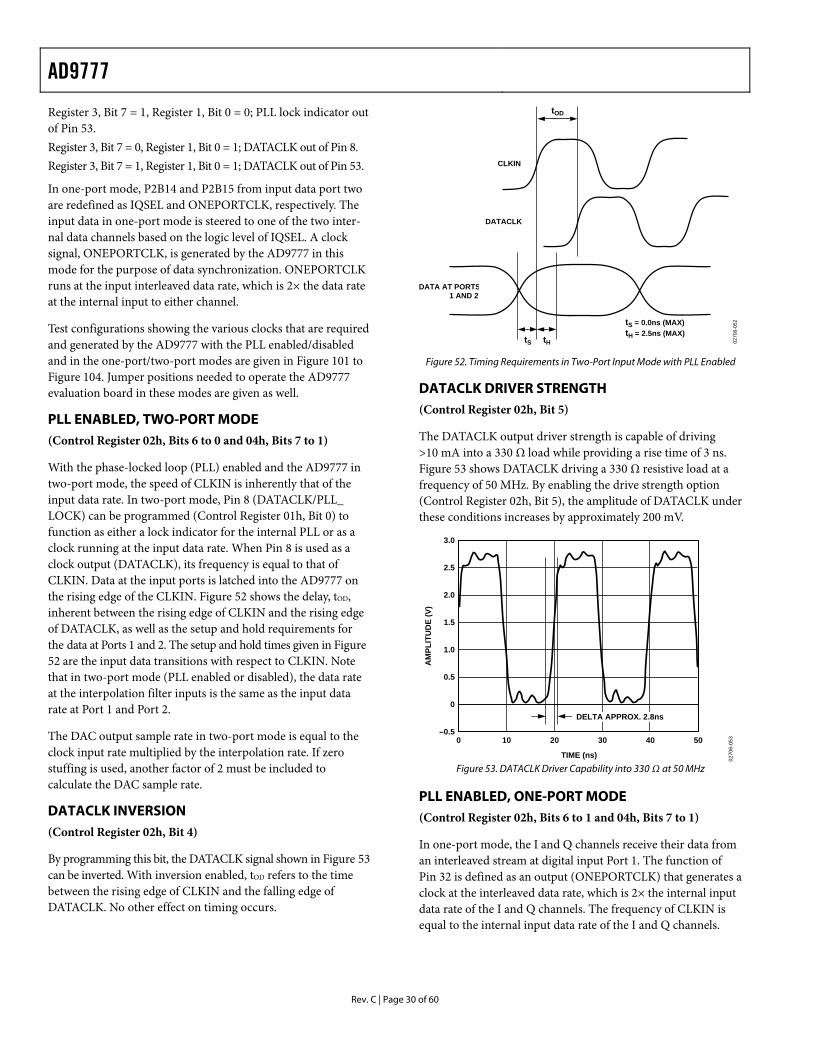
AD9777
Rev. C | Page 30 of 60
Register 3, Bit 7 = 1, Register 1, Bit 0 = 0; PLL lock indicator out of Pin 53. Register 3, Bit 7 = 0, Register 1, Bit 0 = 1; DATACLK out of Pin 8. Register 3, Bit 7 = 1, Register 1, Bit 0 = 1; DATACLK out of Pin 53.
In one-port mode, P2B14 and P2B15 from input data port two are redefined as IQSEL and ONEPORTCLK, respectively. The input data in one-port mode is steered to one of the two inter-nal data channels based on the logic level of IQSEL. A clock signal, ONEPORTCLK, is generated by the AD9777 in this mode for the purpose of data synchronization. ONEPORTCLK runs at the input interleaved data rate, which is 2× the data rate at the internal input to either channel.
Test configurations showing the various clocks that are required and generated by the AD9777 with the PLL enabled/disabled and in the one-port/two-port modes are given in Figure 101 to Figure 104. Jumper positions needed to operate the AD9777 evaluation board in these modes are given as well.
PLL ENABLED, TWO-PORT MODE (Control Register 02h, Bits 6 to 0 and 04h, Bits 7 to 1)
With the phase-locked loop (PLL) enabled and the AD9777 in two-port mode, the speed of CLKIN is inherently that of the input data rate. In two-port mode, Pin 8 (DATACLK/PLL_ LOCK) can be programmed (Control Register 01h, Bit 0) to function as either a lock indicator for the internal PLL or as a clock running at the input data rate. When Pin 8 is used as a clock output (DATACLK), its frequency is equal to that of CLKIN. Data at the input ports is latched into the AD9777 on the rising edge of the CLKIN. Figure 52 shows the delay, tOD, inherent between the rising edge of CLKIN and the rising edge of DATACLK, as well as the setup and hold requirements for the data at Ports 1 and 2. The setup and hold times given in Figure 52 are the input data transitions with respect to CLKIN. Note that in two-port mode (PLL enabled or disabled), the data rate at the interpolation filter inputs is the same as the input data rate at Port 1 and Port 2.
The DAC output sample rate in two-port mode is equal to the clock input rate multiplied by the interpolation rate. If zero stuffing is used, another factor of 2 must be included to calculate the DAC sample rate.
DATACLK INVERSION (Control Register 02h, Bit 4)
By programming this bit, the DATACLK signal shown in Figure 53 can be inverted. With inversion enabled, tOD refers to the time between the rising edge of CLKIN and the falling edge of DATACLK. No other effect on timing occurs.
tOD
tS
tS = 0.0ns (MAX)tH = 2.5ns (MAX)
tH
CLKIN
DATACLK
DATA AT PORTS1 AND 2
0270
6-05
2
Figure 52. Timing Requirements in Two-Port Input Mode with PLL Enabled
DATACLK DRIVER STRENGTH (Control Register 02h, Bit 5)
The DATACLK output driver strength is capable of driving >10 mA into a 330 Ω load while providing a rise time of 3 ns. Figure 53 shows DATACLK driving a 330 Ω resistive load at a frequency of 50 MHz. By enabling the drive strength option (Control Register 02h, Bit 5), the amplitude of DATACLK under these conditions increases by approximately 200 mV.
–0.5
0
0.5
1.0
1.5
2.0
2.5
3.0
AM
PLIT
UD
E (V
)
0 10 20 30 40 50
TIME (ns)
DELTA APPROX. 2.8ns02
706-
053
Figure 53. DATACLK Driver Capability into 330 Ω at 50 MHz
PLL ENABLED, ONE-PORT MODE (Control Register 02h, Bits 6 to 1 and 04h, Bits 7 to 1)
In one-port mode, the I and Q channels receive their data from an interleaved stream at digital input Port 1. The function of Pin 32 is defined as an output (ONEPORTCLK) that generates a clock at the interleaved data rate, which is 2× the internal input data rate of the I and Q channels. The frequency of CLKIN is equal to the internal input data rate of the I and Q channels.
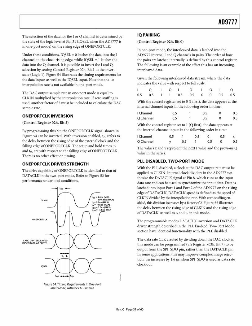
AD9777
Rev. C | Page 31 of 60
The selection of the data for the I or Q channel is determined by the state of the logic level at Pin 31 (IQSEL when the AD9777 is in one-port mode) on the rising edge of ONEPORTCLK.
Under these conditions, IQSEL = 0 latches the data into the I channel on the clock rising edge, while IQSEL = 1 latches the data into the Q channel. It is possible to invert the I and Q selection by setting Control Register 02h, Bit 1 to the invert state (Logic 1). Figure 54 illustrates the timing requirements for the data inputs as well as the IQSEL input. Note that the 1× interpolation rate is not available in one-port mode.
The DAC output sample rate in one-port mode is equal to CLKIN multiplied by the interpolation rate. If zero stuffing is used, another factor of 2 must be included to calculate the DAC sample rate.
ONEPORTCLK INVERSION (Control Register 02h, Bit 2)
By programming this bit, the ONEPORTCLK signal shown in Figure 54 can be inverted. With inversion enabled, tOD refers to the delay between the rising edge of the external clock and the falling edge of ONEPORTCLK. The setup and hold times, tS and tH, are with respect to the falling edge of ONEPORTCLK. There is no other effect on timing.
ONEPORTCLK DRIVER STRENGTH The drive capability of ONEPORTCLK is identical to that of DATACLK in the two-port mode. Refer to Figure 53 for performance under load conditions.
tOD
tS
tIQS tIQH
tOD = 4.0ns (MIN) TO 5.5ns (MAX)tS = 3.0ns (MAX)tH = –0.5ns (MAX)tIQS = 3.5ns (MAX)tIQH = –1.5ns (MAX
tH
CLKIN
ONEPORTCLK
IQSEL
I AND Q INTERLEAVEDINPUT DATA AT PORT 1
0270
6-05
4
Figure 54. Timing Requirements in One-Port
Input Mode, with the PLL Enabled
IQ PAIRING (Control Register 02h, Bit 0)
In one-port mode, the interleaved data is latched into the AD9777 internal I and Q channels in pairs. The order of how the pairs are latched internally is defined by this control register. The following is an example of the effect this has on incoming interleaved data.
Given the following interleaved data stream, where the data indicates the value with respect to full scale:
I Q I Q I Q I Q I Q 0.5 0.5 1 1 0.5 0.5 0 0 0.5 0.5
With the control register set to 0 (I first), the data appears at the internal channel inputs in the following order in time:
I Channel 0.5 1 0.5 0 0.5 Q Channel 0.5 1 0.5 0 0.5
With the control register set to 1 (Q first), the data appears at the internal channel inputs in the following order in time:
I Channel 0.5 1 0.5 0 0.5 x Q Channel y 0.5 1 0.5 0 0.5
The values x and y represent the next I value and the previous Q value in the series.
PLL DISABLED, TWO-PORT MODE With the PLL disabled, a clock at the DAC output rate must be applied to CLKIN. Internal clock dividers in the AD9777 syn-thesize the DATACLK signal at Pin 8, which runs at the input data rate and can be used to synchronize the input data. Data is latched into input Port 1 and Port 2 of the AD9777 on the rising edge of DATACLK. DATACLK speed is defined as the speed of CLKIN divided by the interpolation rate. With zero stuffing en-abled, this division increases by a factor of 2. Figure 55 illustrates the delay between the rising edge of CLKIN and the rising edge of DATACLK, as well as tS and tH in this mode.
The programmable modes DATACLK inversion and DATACLK driver strength described in the PLL Enabled, Two-Port Mode section have identical functionality with the PLL disabled.
The data rate CLK created by dividing down the DAC clock in this mode can be programmed (via Register x03h, Bit 7) to be output from the SPI_SDO pin, rather than the DATACLK pin. In some applications, this may improve complex image rejec-tion. tOD increases by 1.6 ns when SPI_SDO is used as data rate clock out.
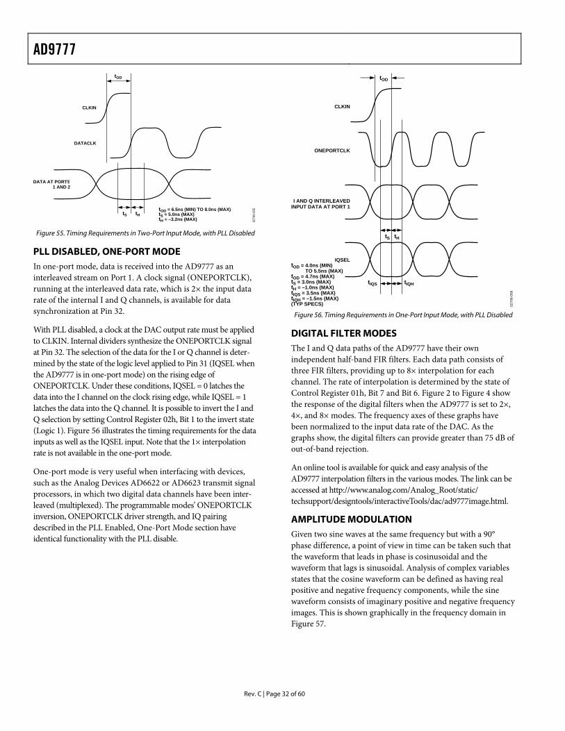
AD9777
Rev. C | Page 32 of 60
tOD
tS tHtOD = 6.5ns (MIN) TO 8.0ns (MAX)tS = 5.0ns (MAX)tH = –3.2ns (MAX)
CLKIN
DATACLK
DATA AT PORTS1 AND 2
0270
6-05
5
Figure 55. Timing Requirements in Two-Port Input Mode, with PLL Disabled
PLL DISABLED, ONE-PORT MODE In one-port mode, data is received into the AD9777 as an interleaved stream on Port 1. A clock signal (ONEPORTCLK), running at the interleaved data rate, which is 2× the input data rate of the internal I and Q channels, is available for data synchronization at Pin 32.
With PLL disabled, a clock at the DAC output rate must be applied to CLKIN. Internal dividers synthesize the ONEPORTCLK signal at Pin 32. The selection of the data for the I or Q channel is deter-mined by the state of the logic level applied to Pin 31 (IQSEL when the AD9777 is in one-port mode) on the rising edge of ONEPORTCLK. Under these conditions, IQSEL = 0 latches the data into the I channel on the clock rising edge, while IQSEL = 1 latches the data into the Q channel. It is possible to invert the I and Q selection by setting Control Register 02h, Bit 1 to the invert state (Logic 1). Figure 56 illustrates the timing requirements for the data inputs as well as the IQSEL input. Note that the 1× interpolation rate is not available in the one-port mode.
One-port mode is very useful when interfacing with devices, such as the Analog Devices AD6622 or AD6623 transmit signal processors, in which two digital data channels have been inter-leaved (multiplexed). The programmable modes’ ONEPORTCLK inversion, ONEPORTCLK driver strength, and IQ pairing described in the PLL Enabled, One-Port Mode section have identical functionality with the PLL disable.
tOD
tS
tIQS tIQH
tH
tOD = 4.0ns (MIN) TO 5.5ns (MAX)tOD = 4.7ns (MAX)tS = 3.0ns (MAX)tH = –1.0ns (MAX)tIQS = 3.5ns (MAX)tIQH = –1.5ns (MAX)(TYP SPECS)
CLKIN
IQSEL
ONEPORTCLK
I AND Q INTERLEAVEDINPUT DATA AT PORT 1
0270
6-05
6
Figure 56. Timing Requirements in One-Port Input Mode, with PLL Disabled
DIGITAL FILTER MODES The I and Q data paths of the AD9777 have their own independent half-band FIR filters. Each data path consists of three FIR filters, providing up to 8× interpolation for each channel. The rate of interpolation is determined by the state of Control Register 01h, Bit 7 and Bit 6. Figure 2 to Figure 4 show the response of the digital filters when the AD9777 is set to 2×, 4×, and 8× modes. The frequency axes of these graphs have been normalized to the input data rate of the DAC. As the graphs show, the digital filters can provide greater than 75 dB of out-of-band rejection.
An online tool is available for quick and easy analysis of the AD9777 interpolation filters in the various modes. The link can be accessed at http://www.analog.com/Analog_Root/static/ techsupport/designtools/interactiveTools/dac/ad9777image.html.
AMPLITUDE MODULATION Given two sine waves at the same frequency but with a 90° phase difference, a point of view in time can be taken such that the waveform that leads in phase is cosinusoidal and the waveform that lags is sinusoidal. Analysis of complex variables states that the cosine waveform can be defined as having real positive and negative frequency components, while the sine waveform consists of imaginary positive and negative frequency images. This is shown graphically in the frequency domain in Figure 57.
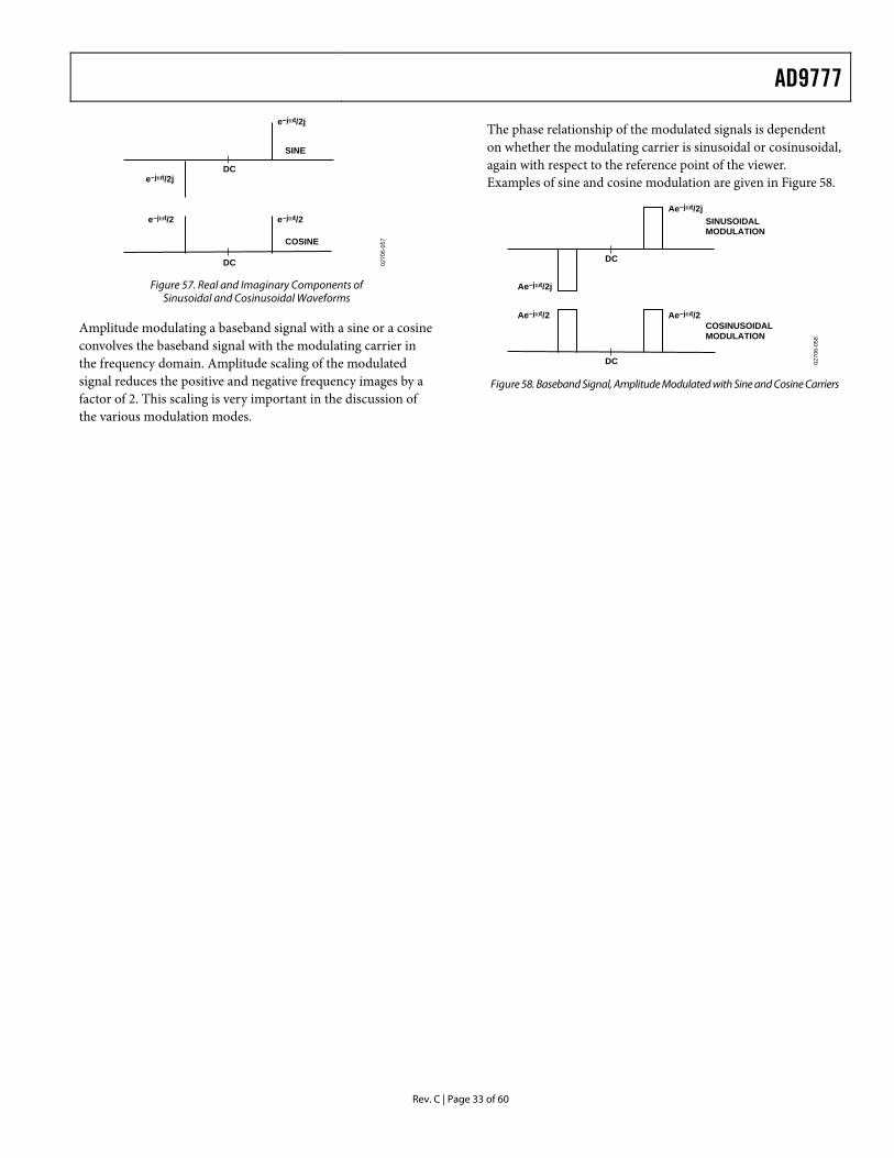
AD9777
Rev. C | Page 33 of 60
e–jωt/2j
e–jωt/2j
e–jωt/2 e–jωt/2
DC
DC
COSINE
SINE
0270
6-05
7
Figure 57. Real and Imaginary Components of
Sinusoidal and Cosinusoidal Waveforms
Amplitude modulating a baseband signal with a sine or a cosine convolves the baseband signal with the modulating carrier in the frequency domain. Amplitude scaling of the modulated signal reduces the positive and negative frequency images by a factor of 2. This scaling is very important in the discussion of the various modulation modes.
The phase relationship of the modulated signals is dependent on whether the modulating carrier is sinusoidal or cosinusoidal, again with respect to the reference point of the viewer. Examples of sine and cosine modulation are given in Figure 58.
DC
SINUSOIDALMODULATION
COSINUSOIDALMODULATION
DC
Ae–jωt/2j
Ae–jωt/2j
Ae–jωt/2 Ae–jωt/2
0270
6-05
8
Figure 58. Baseband Signal, Amplitude Modulated with Sine and Cosine Carriers
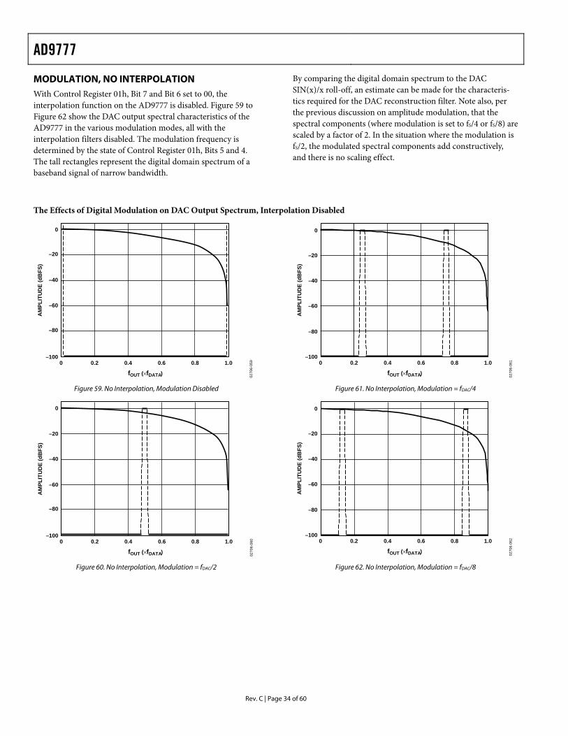
AD9777
Rev. C | Page 34 of 60
MODULATION, NO INTERPOLATION With Control Register 01h, Bit 7 and Bit 6 set to 00, the interpolation function on the AD9777 is disabled. Figure 59 to Figure 62 show the DAC output spectral characteristics of the AD9777 in the various modulation modes, all with the interpolation filters disabled. The modulation frequency is determined by the state of Control Register 01h, Bits 5 and 4. The tall rectangles represent the digital domain spectrum of a baseband signal of narrow bandwidth.
By comparing the digital domain spectrum to the DAC SIN(x)/x roll-off, an estimate can be made for the characteris-tics required for the DAC reconstruction filter. Note also, per the previous discussion on amplitude modulation, that the spectral components (where modulation is set to fS/4 or fS/8) are scaled by a factor of 2. In the situation where the modulation is fS/2, the modulated spectral components add constructively, and there is no scaling effect.
The Effects of Digital Modulation on DAC Output Spectrum, Interpolation Disabled
–100
–80
–60
–40
–20
0
AM
PLIT
UD
E (d
BFS
)
0 0.2 0.4 0.6 0.8 1.0
fOUT (×fDATA)
0270
6-05
9
Figure 59. No Interpolation, Modulation Disabled
–100
–80
–60
–40
–20
0
AM
PLIT
UD
E (d
BFS
)
0 0.2 0.4 0.6 0.8 1.0
fOUT (×fDATA)
0270
6-06
0
Figure 60. No Interpolation, Modulation = fDAC/2
–100
–80
–60
–40
–20
0
AM
PLIT
UD
E (d
BFS
)
0 0.2 0.4 0.6 0.8 1.0
fOUT (×fDATA)
0270
6-06
1
Figure 61. No Interpolation, Modulation = fDAC/4
–100
–80
–60
–40
–20
0
AM
PLIT
UD
E (d
BFS
)
0 0.2 0.4 0.6 0.8 1.0
fOUT (×fDATA)
0270
6-06
2
Figure 62. No Interpolation, Modulation = fDAC/8
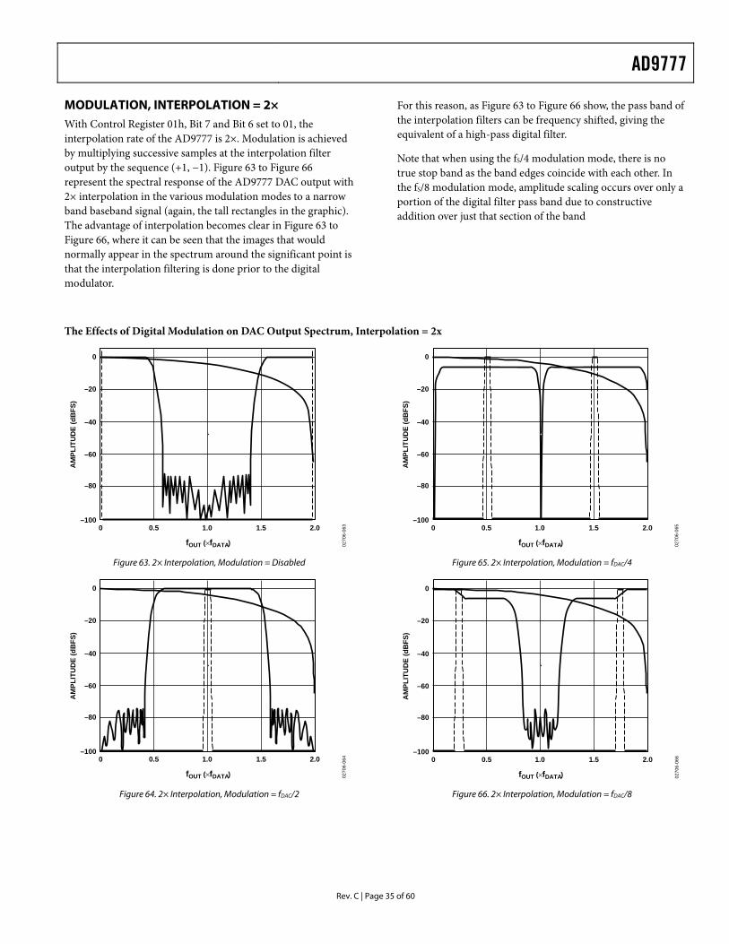
AD9777
Rev. C | Page 35 of 60
MODULATION, INTERPOLATION = 2× With Control Register 01h, Bit 7 and Bit 6 set to 01, the interpolation rate of the AD9777 is 2×. Modulation is achieved by multiplying successive samples at the interpolation filter output by the sequence (+1, −1). Figure 63 to Figure 66 represent the spectral response of the AD9777 DAC output with 2× interpolation in the various modulation modes to a narrow band baseband signal (again, the tall rectangles in the graphic). The advantage of interpolation becomes clear in Figure 63 to Figure 66, where it can be seen that the images that would normally appear in the spectrum around the significant point is that the interpolation filtering is done prior to the digital modulator.
For this reason, as Figure 63 to Figure 66 show, the pass band of the interpolation filters can be frequency shifted, giving the equivalent of a high-pass digital filter.
Note that when using the fS/4 modulation mode, there is no true stop band as the band edges coincide with each other. In the fS/8 modulation mode, amplitude scaling occurs over only a portion of the digital filter pass band due to constructive addition over just that section of the band
The Effects of Digital Modulation on DAC Output Spectrum, Interpolation = 2x
–100
–80
–60
–40
–20
0
AM
PLIT
UD
E (d
BFS
)
fOUT (×fDATA)
0.50 1.0 1.5 2.0
0270
6-06
3
Figure 63. 2× Interpolation, Modulation = Disabled
–100
–80
–60
–40
–20
0
AM
PLIT
UD
E (d
BFS
)
fOUT (×fDATA)
0.50 1.0 1.5 2.0
0270
6-06
4
Figure 64. 2× Interpolation, Modulation = fDAC/2
–100
–80
–60
–40
–20
0
AM
PLIT
UD
E (d
BFS
)
fOUT (×fDATA)
0.50 1.0 1.5 2.0
0270
6-06
5
Figure 65. 2× Interpolation, Modulation = fDAC/4
–100
–80
–60
–40
–20
0
AM
PLIT
UD
E (d
BFS
)
fOUT (×fDATA)
0.50 1.0 1.5 2.0
0270
6-06
6
Figure 66. 2× Interpolation, Modulation = fDAC/8
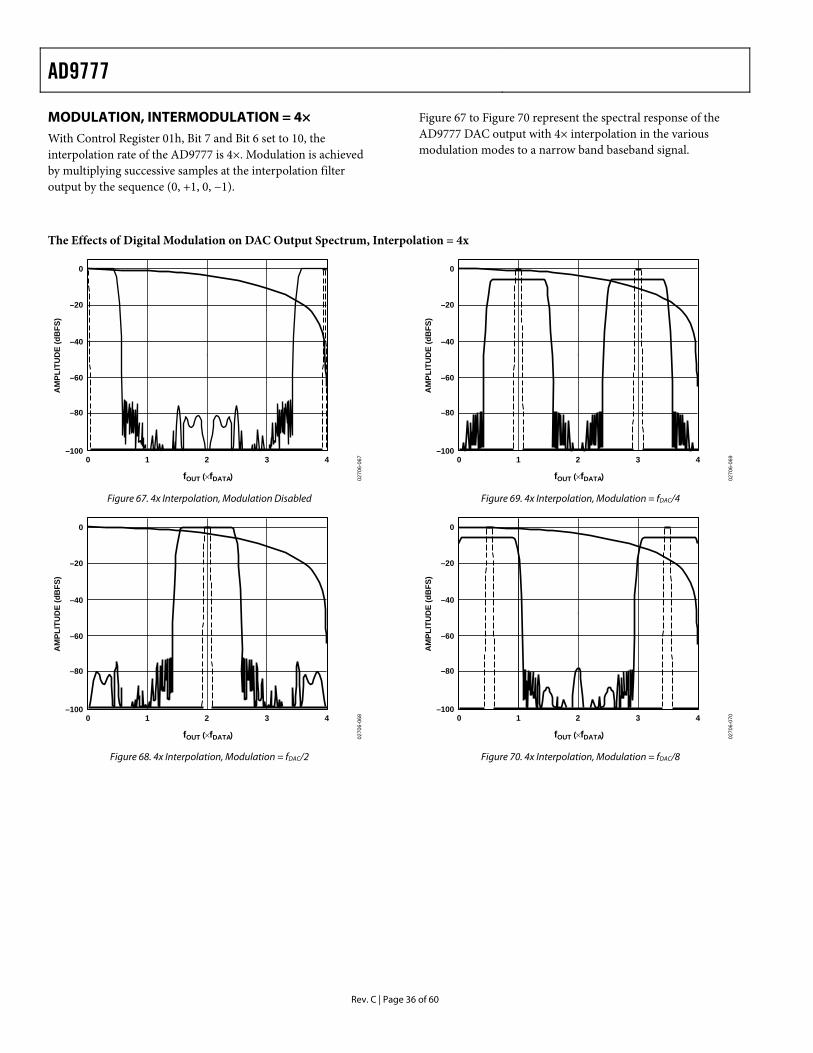
AD9777
Rev. C | Page 36 of 60
MODULATION, INTERMODULATION = 4× With Control Register 01h, Bit 7 and Bit 6 set to 10, the interpolation rate of the AD9777 is 4×. Modulation is achieved by multiplying successive samples at the interpolation filter output by the sequence (0, +1, 0, −1).
Figure 67 to Figure 70 represent the spectral response of the AD9777 DAC output with 4× interpolation in the various modulation modes to a narrow band baseband signal.
The Effects of Digital Modulation on DAC Output Spectrum, Interpolation = 4x
–100
–80
–60
–40
–20
0
AM
PLIT
UD
E (d
BFS
)
fOUT (×fDATA)
10 2 3
0270
6-06
74
Figure 67. 4x Interpolation, Modulation Disabled
–100
–80
–60
–40
–20
0
AM
PLIT
UD
E (d
BFS
)
fOUT (×fDATA)
10 2 3
0270
6-06
84
Figure 68. 4x Interpolation, Modulation = fDAC/2
–100
–80
–60
–40
–20
0
AM
PLIT
UD
E (d
BFS
)
fOUT (×fDATA)
10 2 3
0270
6-06
94
Figure 69. 4x Interpolation, Modulation = fDAC/4
–100
–80
–60
–40
–20
0
AM
PLIT
UD
E (d
BFS
)
fOUT (×fDATA)
10 2 302
706-
0704
Figure 70. 4x Interpolation, Modulation = fDAC/8
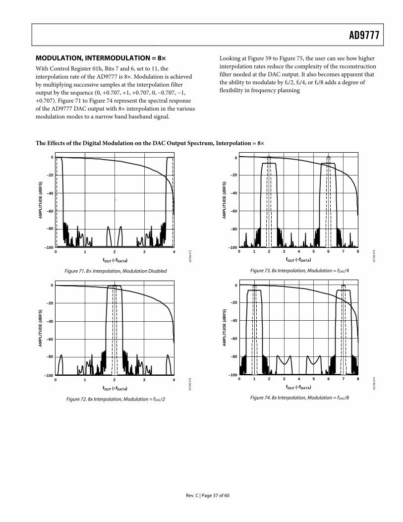
AD9777
Rev. C | Page 37 of 60
MODULATION, INTERMODULATION = 8× With Control Register 01h, Bits 7 and 6, set to 11, the interpolation rate of the AD9777 is 8×. Modulation is achieved by multiplying successive samples at the interpolation filter output by the sequence (0, +0.707, +1, +0.707, 0, –0.707, −1, +0.707). Figure 71 to Figure 74 represent the spectral response of the AD9777 DAC output with 8× interpolation in the various modulation modes to a narrow band baseband signal.
Looking at Figure 59 to Figure 75, the user can see how higher interpolation rates reduce the complexity of the reconstruction filter needed at the DAC output. It also becomes apparent that the ability to modulate by fS/2, fS/4, or fS/8 adds a degree of flexibility in frequency planning
The Effects of the Digital Modulation on the DAC Output Spectrum, Interpolation = 8×
–100
–80
–60
–40
–20
0
AM
PLIT
UD
E (d
BFS
)
fOUT (×fDATA)
10 2 3
0270
6-07
14
Figure 71. 8× Interpolation, Modulation Disabled
–100
–80
–60
–40
–20
0
AM
PLIT
UD
E (d
BFS
)
fOUT (×fDATA)
10 2 3
0270
6-07
24
Figure 72. 8x Interpolation, Modulation = fDAC/2
–100
–80
–60
–40
–20
0
AM
PLIT
UD
E (d
BFS
)
431 20 5 6
fOUT (×fDATA) 0270
6-07
37 8
Figure 73. 8x Interpolation, Modulation = fDAC/4
–100
–80
–60
–40
–20
0
AM
PLIT
UD
E (d
BFS
)
431 20 5 6 7
fOUT (×fDATA) 0270
6-07
48
Figure 74. 8x Interpolation, Modulation = fDAC/8
AD9777
Rev. C | Page 38 of 60
ZERO STUFFING (Control Register 01h, Bit 3)
As shown in Figure 75, a 0 or null in the output frequency response of the DAC (after interpolation, modulation, and DAC reconstruction) occurs at the final DAC sample rate (fDAC). This is due to the inherent SIN(x)/x roll-off response in the digital-to-analog conversion. In applications where the desired fre-quency content is below fDAC/2, this may not be a problem. Note that at fDAC/2 the loss due to SIN(x)/x is 4 dB. In direct RF appli-cations, this roll-off may be problematic due to the increased pass-band amplitude variation as well as the reduced amplitude of the desired signal.
Consider an application where the digital data into the AD9777 represents a baseband signal around fDAC/4 with a pass band of fDAC/10. The reconstructed signal out of the AD9777 would experience only a 0.75 dB amplitude variation over its pass band. However, the image of the same signal occurring at 3× fDAC/4 suffers from a pass-band flatness variation of 3.93 dB. This image may be the desired signal in an IF application using one of the various modulation modes in the AD9777. This roll-off of image frequencies can be seen in Figure 59 to Figure 74, where the effect of the interpolation and modulation rate is apparent as well.
–50
–40
–30
–20
–10
0
10
SIN
(X)/X
RO
LL-O
FF (d
BFS
)
fOUT, NORMALIZED TO fDATA WITH ZERO STUFFING DISABLED (Hz)
0.50 1.0 1.5 2.0
ZERO STUFFINGENABLED
ZERO STUFFINGDISABLED
0270
6-07
5
Figure 75. Effect of Zero Stuffing on DAC’s SIN(x)/x Response
To improve upon the pass-band flatness of the desired image, the zero stuffing mode can be enabled by setting the control register bit to a Logic 1. This option increases the ratio of fDAC/fDATA by a factor of 2 by doubling the DAC sample rate and inserting a midscale sample (that is, 1000 0000 0000 0000) after every data sample originating from the interpolation filter. This is important as it affects the PLL divider ratio needed to keep the VCO within its optimum speed range. Note that the zero stuffing takes place in the digital signal chain at the output of the digital modulator, before the DAC.
The net effect is to increase the DAC output sample rate by a factor of 2× with the 0 in the SIN(x)/x DAC transfer function occurring at twice the original frequency. A 6 dB loss in amplitude at low frequencies is also evident, as can be seen in Figure 76.
It is important to realize that the zero stuffing option by itself does not change the location of the images but rather their amplitude, pass-band flatness, and relative weighting. For instance, in the previous example, the pass-band amplitude flatness of the image at 3× fDATA/4 is now improved to 0.59 dB while the signal level has increased slightly from −10.5 dBFS to –8.1 dBFS.
INTERPOLATING (COMPLEX MIX MODE) (Control Register 01h, Bit 2)
In the complex mix mode, the two digital modulators on the AD9777 are coupled to provide a complex modulation function. In conjunction with an external quadrature modulator, this complex modulation can be used to realize a transmit image rejection architecture. The complex modulation function can be programmed for e+jωt or e−jωt to give upper or lower image rejection. As in the real modulation mode, the modulation frequency ω can be programmed via the SPI port for fDAC/2, fDAC/4, and fDAC/8, where fDAC represents the DAC output rate.
OPERATIONS ON COMPLEX SIGNALS Truly complex signals cannot be realized outside of a computer simulation. However, two data channels, both consisting of real data, can be defined as the real and imaginary components of a complex signal. I (real) and Q (imaginary) data paths are often defined this way. By using the architecture defined in Figure 76, a system that operates on complex signals can be realized, giving a complex (real and imaginary) output.
If a complex modulation function (e+jωt) is desired, the real and imaginary components of the system correspond to the real and imaginary components of e+jωt or cosωt and sinωt. As Figure 77 shows, the complex modulation function can be realized by applying these components to the structure of the complex system defined in Figure 76.
a(t)
= (c + jd)
b(t)
c(t) × b(t) + d × b(t)
b(t) × a(t) + c × b(t)
INPUT OUTPUT
INPUT OUTPUT
COMPLEX FILTER
IMAGINARY
0270
6-07
6
Figure 76. Realization of a Complex System
AD9777
Rev. C | Page 39 of 60
INPUT(REAL) OUTPUT
(REAL)
OUTPUT(IMAGINARY)
INPUT(IMAGINARY)
90°
e–jωt = COSωt + jSINωt 0270
6-07
7
Figure 77. Implementation of a Complex Modulator
COMPLEX MODULATION AND IMAGE REJECTION OF BASEBAND SIGNALS In traditional transmit applications, a two-step upconversion is done in which a baseband signal is modulated by one carrier to an IF (intermediate frequency) and then modulated a second time to the transmit frequency. Although this approach has several benefits, a major drawback is that two images are created near the transmit frequency. Only one image is needed, the other being an exact duplicate. Unless the unwanted image is filtered, typically with analog components, transmit power is wasted and the usable bandwidth available in the system is reduced.
A more efficient method of suppressing the unwanted image can be achieved by using a complex modulator followed by a quadrature modulator. Figure 78 is a block diagram of a quadrature modulator. Note that it is in fact the real output half of a complex modulator. The complete upconversion can actually be referred to as two complex upconversion stages, the real output of which becomes the transmitted signal.
INPUT(REAL)
OUTPUTINPUT
(IMAGINARY)
90° COSωtSINωt
0270
6-07
8
Figure 78. Quadrature Modulation
The entire upconversion from baseband to transmit frequency is represented graphically in Figure 79. The resulting spectrum shown in Figure 79 represents the complex data consisting of the baseband real and imaginary channels, now modulated onto orthogonal (cosine and negative sine) carriers at the transmit frequency. It is important to remember that in this application (two baseband data channels), the image rejection is not dependent on the data at either of the AD9777 input channels.
In fact, image rejection still occurs with either one or both of the AD9777 input channels active. Note that by changing the sign of the sinusoidal multiplying term in the complex modulator, the upper sideband image could have been suppressed while passing the lower one. This is easily done in the AD9777 by selecting the e+jωt bit (Register 01h, Bit 1). In purely complex terms, Figure 79 represents the two-stage upconversion from complex baseband to carrier.
AD9777
Rev. C | Page 40 of 60
REAL CHANNEL (OUT)
IMAGINARY CHANNEL (OUT)
A/2
–B/2J B/2J
–A/2J A/2J
–FC1 FC
FC–FC
–FC
–FC FC
–FC
A/2
B/2 B/2
COMPLEXMODULATOR
TO QUADRATUREMODULATOR
REAL CHANNEL (IN)
IMAGINARY CHANNEL (IN)
A
DC
B
DC
A/4 + B/4J A/4 – B/4J A/4 + B/4J A/4 – B/4J
–A/4 – B/4J
A/2 + B/2J A/2 – B/2J
A/4 – B/4J A/4 + B/4J –A/4 + B/4J
–FQ – FC –FQ + FC
–FQ2
–FQ FQ
–FQ FQ
FQ – FC FQ + FC
FQ
QUADRATUREMODULATOR
OUTREAL
IMAGINARY
REJECTED IMAGES
1FC = COMPLEX MODULATION FREQUENCY2FQ = QUADRATURE MODULATION FREQUENCY 02
706-
079
Figure 79. Two-Stage Upconversion and Resulting Image Rejection
AD9777
Rev. C | Page 41 of 60
COMPLEX BASEBANDSIGNAL
OUTPUT = REAL
= REAL
FREQUENCY
1
1/2 1/2
–ω1 – ω2 DC
× ej(ω1 + ω2)t
ω1 + ω2
0270
6-08
0
Figure 80. Two-Stage Complex Upconversion
IMAGE REJECTION AND SIDEBAND SUPPRESSIONS OF MODULATED CARRIERS As shown in Figure 79, image rejection can be achieved by applying baseband data to the AD9777 and following the AD9777 with a quadrature modulator. To process multiple carriers while still maintaining image reject capability, each carrier must be complex modulated. As Figure 80 shows, single or multiple complex modulators can be used to synthesize complex carriers. These complex carriers are then summed and applied to the real and imaginary inputs of the AD9777.
A system in which multiple baseband signals are complex modulated and then applied to the AD9777 real and imaginary inputs, followed by a quadrature modulator, is shown in Figure 82, which also describes the transfer function of this system and the spectral output. Note the similarity of the transfer functions given in Figure 82 and Figure 80. Figure 82 adds an additional complex modulator stage for summing multiple carriers at the AD9777 inputs. In addition, as in Figure 79, the image rejection is not dependent on the real or imaginary baseband data on any channel. Image rejection on a channel occurs if either the real or imaginary data, or both, is present on the baseband channel.
It is important to remember that the magnitude of a complex signal can be 1.414× the magnitude of its real or imaginary components. Due to this 3 dB increase in signal amplitude, the real and imaginary inputs to the AD9777 must be kept at least 3 dB below full scale when operating with the complex modulator. Overranging in the complex modulator results in severe distortion at the DAC output.
BASEBAND CHANNEL 1REAL INPUT
BASEBAND CHANNEL 2REAL INPUT
BASEBAND CHANNEL NREAL INPUT
IMAGINARY INPUT
IMAGINARY INPUT
IMAGINARY INPUT
COMPLEXMODULATOR 1
COMPLEXMODULATOR 2
COMPLEXMODULATOR N
R(1)
R(1)
R(2)
R(2)
R(N)
R(N)
MULTICARRIERREAL OUTPUT =R(1) + R(2) + . . .R(N)(TO REAL INPUT OF AD9777)
MULTICARRIERIMAGINARY OUTPUT =I(1) + I(2) + . . .I(N)(TO IMAGINARY INPUT OF AD9777)
R(N) = REAL OUTPUT OF NI(N) = IMAGINARY OUTPUT OF N
0270
6-08
1
Figure 81. Synthesis of Multicarrier Complex Signal
MULTIPLEBASEBANDCHANNELS
MULTIPLECOMPLEX
MODULATORSFREQUENCY = ω1, ω2...ωN
REAL
IMAGINARY
REAL
OUTPUT = REAL
IMAGINARY
REAL REAL
IMAGINARY
AD9777COMPLEX
MODULATORFREQUENCY = ωC
QUADRATUREMODULATOR
FREQUENCY = ωQ
COMPLEX BASEBANDSIGNAL
REJECTED IMAGES
DC
× ej(ωN + ωC + ωQ)t
–ω1 – ωC – ωQ ω1 + ωC + ωQ
0270
6-08
2
Figure 82. Image Rejection with Multicarrier Signals
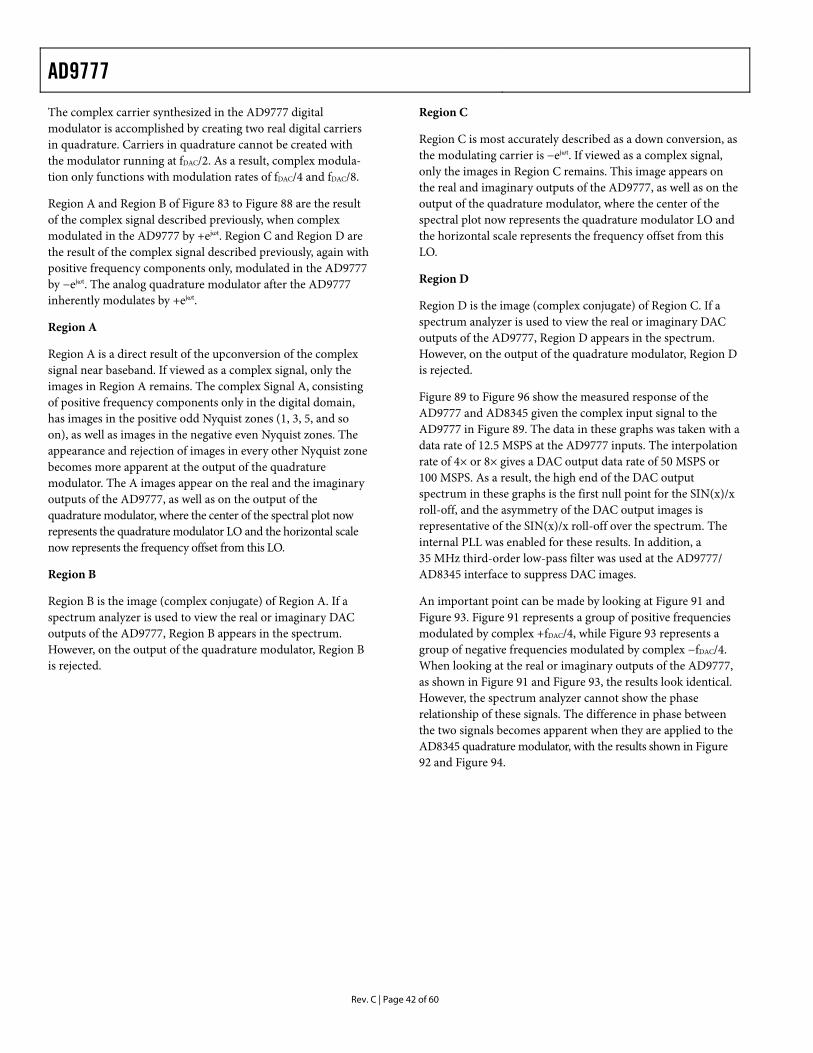
AD9777
Rev. C | Page 42 of 60
The complex carrier synthesized in the AD9777 digital modulator is accomplished by creating two real digital carriers in quadrature. Carriers in quadrature cannot be created with the modulator running at fDAC/2. As a result, complex modula-tion only functions with modulation rates of fDAC/4 and fDAC/8.
Region A and Region B of Figure 83 to Figure 88 are the result of the complex signal described previously, when complex modulated in the AD9777 by +ejωt. Region C and Region D are the result of the complex signal described previously, again with positive frequency components only, modulated in the AD9777 by −ejωt. The analog quadrature modulator after the AD9777 inherently modulates by +ejωt.
Region A
Region A is a direct result of the upconversion of the complex signal near baseband. If viewed as a complex signal, only the images in Region A remains. The complex Signal A, consisting of positive frequency components only in the digital domain, has images in the positive odd Nyquist zones (1, 3, 5, and so on), as well as images in the negative even Nyquist zones. The appearance and rejection of images in every other Nyquist zone becomes more apparent at the output of the quadrature modulator. The A images appear on the real and the imaginary outputs of the AD9777, as well as on the output of the quadrature modulator, where the center of the spectral plot now represents the quadrature modulator LO and the horizontal scale now represents the frequency offset from this LO.
Region B
Region B is the image (complex conjugate) of Region A. If a spectrum analyzer is used to view the real or imaginary DAC outputs of the AD9777, Region B appears in the spectrum. However, on the output of the quadrature modulator, Region B is rejected.
Region C
Region C is most accurately described as a down conversion, as the modulating carrier is −ejωt. If viewed as a complex signal, only the images in Region C remains. This image appears on the real and imaginary outputs of the AD9777, as well as on the output of the quadrature modulator, where the center of the spectral plot now represents the quadrature modulator LO and the horizontal scale represents the frequency offset from this LO.
Region D
Region D is the image (complex conjugate) of Region C. If a spectrum analyzer is used to view the real or imaginary DAC outputs of the AD9777, Region D appears in the spectrum. However, on the output of the quadrature modulator, Region D is rejected.
Figure 89 to Figure 96 show the measured response of the AD9777 and AD8345 given the complex input signal to the AD9777 in Figure 89. The data in these graphs was taken with a data rate of 12.5 MSPS at the AD9777 inputs. The interpolation rate of 4× or 8× gives a DAC output data rate of 50 MSPS or 100 MSPS. As a result, the high end of the DAC output spectrum in these graphs is the first null point for the SIN(x)/x roll-off, and the asymmetry of the DAC output images is representative of the SIN(x)/x roll-off over the spectrum. The internal PLL was enabled for these results. In addition, a 35 MHz third-order low-pass filter was used at the AD9777/ AD8345 interface to suppress DAC images.
An important point can be made by looking at Figure 91 and Figure 93. Figure 91 represents a group of positive frequencies modulated by complex +fDAC/4, while Figure 93 represents a group of negative frequencies modulated by complex −fDAC/4. When looking at the real or imaginary outputs of the AD9777, as shown in Figure 91 and Figure 93, the results look identical. However, the spectrum analyzer cannot show the phase relationship of these signals. The difference in phase between the two signals becomes apparent when they are applied to the AD8345 quadrature modulator, with the results shown in Figure 92 and Figure 94.
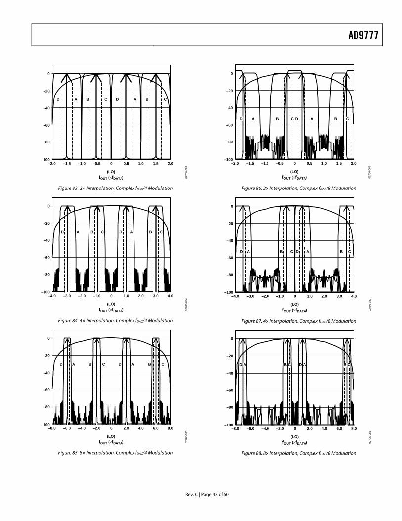
AD9777
Rev. C | Page 43 of 60
–100
–80
–60
–40
–20
0
0–0.5–1.5 –1.0–2.0 0.5 1.0 1.5 2.0
(LO)fOUT (×fDATA)
D A B C D A B C
0270
6-08
3
Figure 83. 2× Interpolation, Complex fDAC/4 Modulation
–100
–80
–60
–40
–20
0
0–1.0–3.0 –2.0–4.0 1.0 2.0 3.0 4.0
(LO)fOUT (×fDATA)
D A B C D A B C
0270
6-08
4
Figure 84. 4× Interpolation, Complex fDAC/4 Modulation
–100
–80
–60
–40
–20
0
0–2.0–6.0 –4.0–8.0 2.0 4.0 6.0 8.0
(LO)fOUT (×fDATA)
D A B C D A B C
0270
6-08
5
Figure 85. 8× Interpolation, Complex fDAC/4 Modulation
–100
–80
–60
–40
–20
0
0–0.5–1.5 –1.0–2.0 0.5 1.0 1.5 2.0
(LO)fOUT (×fDATA)
D A B C D A B C
0270
6-08
6
Figure 86. 2× Interpolation, Complex fDAC/8 Modulation
–100
–80
–60
–40
–20
0
0–1.0–3.0 –2.0–4.0 1.0 2.0 3.0 4.0
(LO)fOUT (×fDATA)
D A B C D A B C
0270
6-08
7
Figure 87. 4× Interpolation, Complex fDAC/8 Modulation
–100
–80
–60
–40
–20
0
0–2.0–6.0 –4.0–8.0 2.0 4.0 6.0 8.0
(LO)fOUT (×fDATA)
D A D AB C B C02
706-
088
Figure 88. 8× Interpolation, Complex fDAC/8 Modulation
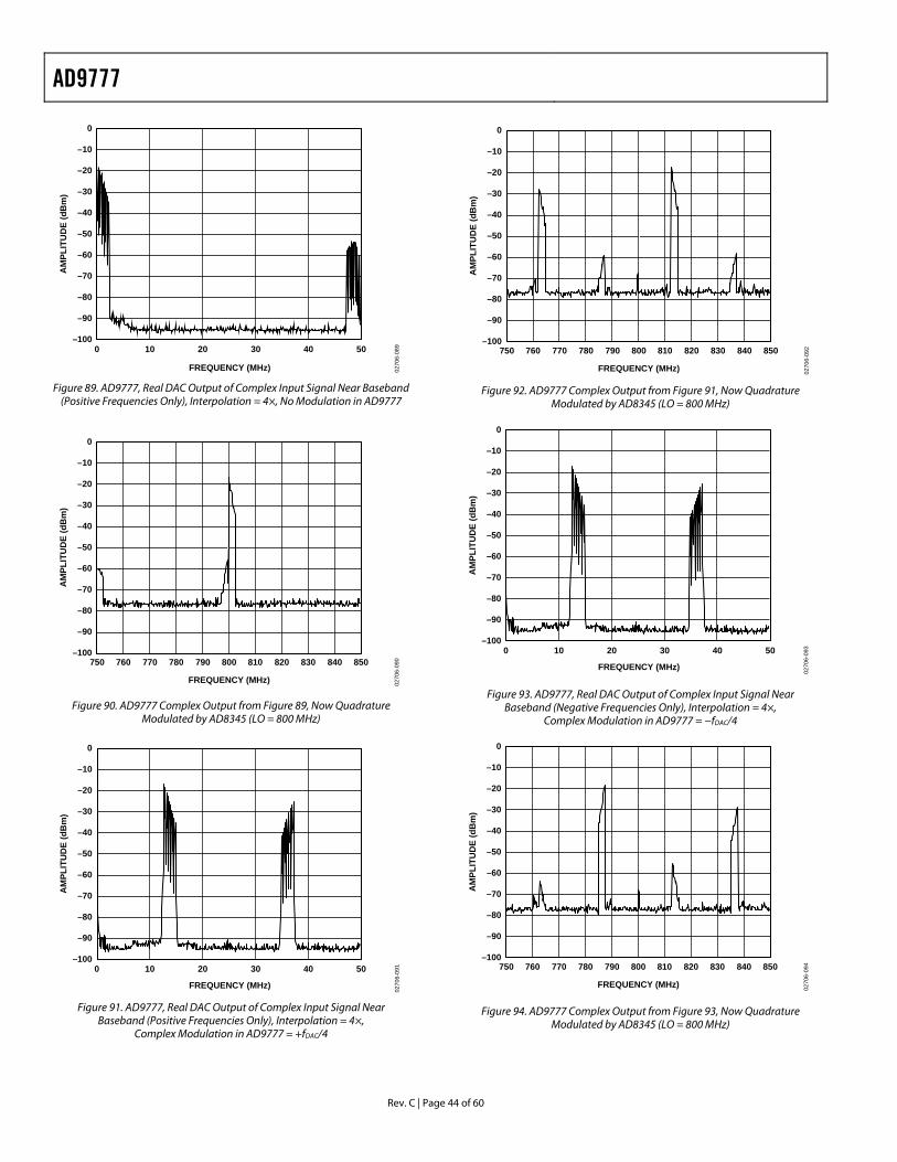
AD9777
Rev. C | Page 44 of 60
0 10 20 30 40 50–100
–90
–80
–70
–60
–50
–40
–30
–20
–10
0
AM
PLIT
UD
E (d
Bm
)
FREQUENCY (MHz) 0270
6-08
9
Figure 89. AD9777, Real DAC Output of Complex Input Signal Near Baseband (Positive Frequencies Only), Interpolation = 4×, No Modulation in AD9777
–100
–90
–80
–70
–60
–50
–40
–30
–20
–10
0
AM
PLIT
UD
E (d
Bm
)
750 760 770 780 790 800 810 820 830 840 850
FREQUENCY (MHz) 0270
6-09
0
Figure 90. AD9777 Complex Output from Figure 89, Now Quadrature Modulated by AD8345 (LO = 800 MHz)
–100
–90
–80
–70
–60
–50
–40
–30
–20
–10
0
AM
PLIT
UD
E (d
Bm
)
0 10 20 30 40 50
FREQUENCY (MHz)
0270
6-09
1
Figure 91. AD9777, Real DAC Output of Complex Input Signal Near Baseband (Positive Frequencies Only), Interpolation = 4×,
Complex Modulation in AD9777 = +fDAC/4
–100
–90
–80
–70
–60
–50
–40
–30
–20
–10
0
AM
PLIT
UD
E (d
Bm
)
750 760 770 780 790 800 810 820 830 840 850
FREQUENCY (MHz) 0270
6-09
2
Figure 92. AD9777 Complex Output from Figure 91, Now Quadrature Modulated by AD8345 (LO = 800 MHz)
–100
–90
–80
–70
–60
–50
–40
–30
–20
–10
0
AM
PLIT
UD
E (d
Bm
)
0 10 20 30 40 50
FREQUENCY (MHz)
0270
6-09
3
Figure 93. AD9777, Real DAC Output of Complex Input Signal Near Baseband (Negative Frequencies Only), Interpolation = 4×,
Complex Modulation in AD9777 = −fDAC/4
–100
–90
–80
–70
–60
–50
–40
–30
–20
–10
0
AM
PLIT
UD
E (d
Bm
)
750 760 770 780 790 800 810 820 830 840 850
FREQUENCY (MHz) 0270
6-09
4
Figure 94. AD9777 Complex Output from Figure 93, Now Quadrature Modulated by AD8345 (LO = 800 MHz)
AD9777
Rev. C | Page 45 of 60
–100
–80
–60
–40
–20
0
AM
PLIT
UD
E (d
Bm
)
0 20 40 60 80 100
FREQUENCY (MHz)
0270
6-09
5
Figure 95. AD9777, Real DAC Output of Complex Input Signal Near
Baseband (Positive Frequencies Only), Interpolation = 8×, Complex Modulation in AD9777 = +fDAC/8
–100
–90
–80
–70
–60
–50
–40
–30
–20
–10
0
AM
PLIT
UD
E (d
Bm
)
700 720 740 760 780 800 820 840 860 880 900
FREQUENCY (MHz) 0270
6-09
6
Figure 96. AD9777 Complex Output from Figure 95, Now Quadrature
Modulated by AD8345 (LO = 800 MHz)
AD9777
Rev. C | Page 46 of 60
APPLYING THE OUTPUT CONFIGURATIONS The following sections illustrate typical output configurations for the AD9777. Unless otherwise noted, it is assumed that IOUTFS is set to a nominal 20 mA. For applications requiring optimum dynamic performance, a differential output configu-ration is suggested. A simple differential output may be achieved by converting IOUTA and IOUTB to a voltage output by terminating them to AGND via equal value resistors. This type of configuration may be useful when driving a differential voltage input device such as a modulator. If a conversion to a single-ended signal is desired and the application allows for ac coupling, an RF transformer may be useful; if power gain is required, an op amp may be used. The transformer configura-tion provides optimum high frequency noise and distortion performance. The differential op amp configuration is suitable for applications requiring dc coupling, signal gain, and/or level shifting within the bandwidth of the chosen op amp.
A single-ended output is suitable for applications requiring a unipolar voltage output. A positive unipolar output voltage results if IOUTA and/or IOUTB is connected to a load resistor, RLOAD, referred to AGND. This configuration is most suitable for a single-supply system requiring a dc-coupled, ground referred output voltage. Alternatively, an amplifier could be configured as an I-V converter, thus converting IOUTA or IOUTB into a negative unipolar voltage. This configuration provides the best DAC dc linearity as IOUTA or IOUTB are maintained at ground or virtual ground.
UNBUFFERED DIFFERENTIAL OUTPUT, EQUIVALENT CIRCUIT In many applications, it may be necessary to understand the equivalent DAC output circuit. This is especially useful when designing output filters or when driving inputs with finite input impedances. Figure 97 illustrates the output of the AD9777 and the equivalent circuit. A typical application where this information may be useful is when designing an interface filter between the AD9777 and the Analog Devices AD8345 quadrature modulator.
IOUTA
IOUTB
VOUT+
VOUT(DIFFERENTIAL)
VSOURCE =IOUTFS × (RA + RB)
p-p
VOUT–
RA + RB
0270
6-09
7
Figure 97. DAC Output Equivalent Circuit
For the typical situation, where IOUTFS = 20 mA and RA and RB both equal 50 Ω, the equivalent circuit values become
VSOURCE = 2 VP-P
ROUT = 100 Ω
Note that the output impedance of the AD9777 DAC itself is greater than 100 kΩ and typically has no effect on the impedance of the equivalent output circuit.
DIFFERENTIAL COUPLING USING A TRANSFORMER An RF transformer can be used to perform a differential-to-single-ended signal conversion, as shown in Figure 98. A differentially coupled transformer output provides the optimum distortion performance for output signals whose spectral content lies within the transformer’s pass band. An RF transformer, such as the Mini-Circuits T1-1T, provides excellent rejection of common-mode distortion (that is, even-order harmonics) and noise over a wide frequency range. It also provides electrical isolation and the ability to deliver twice the power to the load. Transformers with different impedance ratios may also be used for impedance matching purposes.
MINI-CIRCUITST1-1T
RLOAD
IOUTA
IOUTB
DAC
0270
6-09
8
Figure 98. Transformer-Coupled Output Circuit
The center tap on the primary side of the transformer must be connected to AGND to provide the necessary dc current path for both IOUTA and IOUTB. The complementary voltages appearing at IOUTA and IOUTB (that is, VOUTA and VOUTB) swing symmetrically around AGND and should be maintained within the specified output compliance range of the AD9777. A differential resistor, RDIFF, can be inserted in applications where the output of the transformer is connected to the load, RLOAD, via a passive reconstruction filter or cable. RDIFF is determined by the transformer’s impedance ratio and provides the proper source termination that results in a low VSWR. Note that approxi-mately half the signal power dissipates across RDIFF.
AD9777
Rev. C | Page 47 of 60
DIFFERENTIAL COUPLING USING AN OP AMP An op amp can also be used to perform a differential-to-single ended conversion, as shown in Figure 99. This has the added benefit of providing signal gain as well. In Figure 99, the AD9777 is configured with two equal load resistors, RLOAD, of 25 Ω. The differential voltage developed across IOUTA and IOUTB is converted to a single-ended signal via the differential op amp configuration. An optional capacitor can be installed across IOUTA and IOUTB, forming a real pole in a low-pass filter. The addition of this capacitor also enhances the op amp’s distortion performance by preventing the DAC’s fast slewing output from overloading the input of the op amp.
IOUTA
IOUTB COPT
ROPT225Ω
DAC
225Ω
225Ω
500Ω
500Ω
25Ω 25Ω
AVDD
AD802102
706-
099
Figure 99. Op Amp-Coupled Output Circuit
The common-mode (and second-order distortion) rejection of this configuration is typically determined by the resistor matching. The op amp used must operate from a dual supply since its output is approximately ±1.0 V. A high speed amplifier, such as the AD8021, capable of preserving the differential performance of the AD9777 while meeting other system level objectives (for example, cost, power) is recommended. The op amp’s differential gain, gain setting resistor values, and full-scale output swing capabilities should all be considered when optimizing this circuit. ROPT is necessary only if level shifting is required on the op amp output. In Figure 99, AVDD, which is the positive analog supply for both the AD9777 and the op amp, is also used to level shift the differential output of the AD9777 to midsupply (that is, AVDD/2).
INTERFACING WITH THE AD8345 QUADRATURE MODULATOR The AD9777 architecture was defined to operate in a transmit signal chain using an image reject architecture. A quadrature modulator is also required in this application and should be designed to meet the output characteristics of the DAC as much as possible. The AD8345 from Analog Devices meets many of the requirements for interfacing with the AD9777. As with any DAC output interface, there are a number of issues that have to be resolved. The following sections list some of the major issues.
DAC Compliance Voltage/Input Common-Mode Range
The dynamic range of the AD9777 is optimal when the DAC outputs swing between ±1.0 V. The input common-mode range of the AD8345, at 0.7 V, allows optimum dynamic range to be achieved in both components.
Gain/Offset Adjust
The matching of the DAC output to the common-mode input of the AD8345 allows the two components to be dc-coupled, with no level shifting necessary. The combined voltage offset of the two parts can therefore be compensated via the AD9777 programmable offset adjust. This allows excellent LO cancellation at the AD8345 output. The programmable gain adjust allows for optimal image rejection as well.
The AD9777 evaluation board includes an AD8345 and recommended interface (Figure 105 and Figure 106). On the output of the AD9777, R9 and R10 convert the DAC output current to a voltage. R16 can be used to do a slight common-mode shift if necessary. The (now voltage) signal is applied to a low-pass reconstruction filter to reject DAC images. The components installed on the AD9777 provide a 35 MHz cutoff but can be changed to fit the application. A balun (Mini-Circuits ADTL1-12) is used to cross the ground plane boundary to the AD8345. Another balun (Mini-Circuits ETC1-1-13) is used to couple the LO input of the AD8345. The interface requires a low ac impedance return path from the AD8345, therefore a single connection between the AD9777 and AD8345 ground planes is recommended.
The performance of the AD9777 and AD8345 in an image reject transmitter, reconstructing three WCDMA carriers, can be seen in Figure 100. The LO of the AD8345 in this application is 800 MHz. Image rejection (50 dB) and LO feedthrough (−78 dBFS) have been optimized with the programmable features of the AD9777. The average output power of the digital waveform for this test was set to −15 dBFS to account for the peak-to-average ratio of the WCDMA signal.
–100
–90
–80
–70
–60
–50
–40
–30
–20
–10
0
AM
PLIT
UD
E (d
Bm
)
FREQUENCY (MHz)
782.5762.5 802.5 822.5 842.5
0270
6-10
0
Figure 100. AD9777/AD8345 Synthesizing a
Three-Carrier WCDMA Signal at an LO of 800 MHz

AD9777
Rev. C | Page 48 of 60
EVALUATION BOARDThe AD9777 evaluation board allows easy configuration of the various modes, programmable via the SPI port. Software is available for programming the SPI port from Windows® 95, Windows 98, or Windows NT®/2000. The evaluation board also contains an AD8345 quadrature modulator and support circuitry that allows the user to optimally configure the AD9777 in an image reject transmit signal chain.
Figure 101 to Figure 104 describe how to configure the evaluation board in the one-port and two-port input modes with the PLL enabled and disabled. Refer to Figure 105 to Figure 114, the schematics, and the layout for the AD9777 evaluation board for the jumper locations described below. The AD9777 outputs can be configured for various applications by referring to the following instructions.
DAC Single-Ended Outputs
Remove Transformers T2 and T3. Solder jumper link JP4 or JP28 to look at the DAC1 outputs. Solder jumper link JP29 or JP30 to look at the DAC2 outputs. Jumpers 8 and 13 to 17 should remain unsoldered. Jumpers JP35 to JP38 may be used to ground one of the DAC outputs while the other is measured single-ended. Optimum single-ended distortion performance is typically achieved in this manner. The outputs are taken from S3 and S4.
DAC Differential Outputs
Transformers T2 and T3 should be in place. Note that the lower band of operation for these transformers is 300 kHz to 500 kHz. Jumpers 4, 8, 13 to 17, and 28 to 30 should remain unsoldered. The outputs are taken from S3 and S4.
Using the AD8345
Remove Transformers T2 and T3. Jumpers JP4 and 28 to 30 should remain unsoldered. Jumpers 13 to 16 should be soldered. The desired components for the low-pass interface filters L6, L7, C55, and C81 should be in place. The LO drive is connected to the AD8345 via J10 and the balun T4, and the AD8345 output is taken from J9.
AD9777
Rev. C | Page 49 of 60
SIGNAL GENERATOR
CLK+/CLK–DATACLK
LECROYPULSEGENERATOR
TRIGINP
AWG2021OR
DG2020
INPUT CLOCK
DAC1, DB15–DB0
AD9777DAC2, DB15–DB0
40-PIN RIBBON CABLE
JUMPER CONFIGURATION FOR TWO PORT MODE PLL ON
JP1 –JP2 –JP3 –JP5 –JP6 –
JP12 –JP24 –JP25 –JP26 –JP27 –JP31 –JP32 –JP33 –
SOLDERED/IN×
××
××
UNSOLDERED/OUT
×
×××
××××
0270
6-10
1
NOTES1. TO USE PECL CLOCK DRIVER (U8), SOLDER JP41 AND JP42 AND REMOVE TRANSFORMER T1.2. IN TWO-PORT MODE, IF DATACLK/PLL_LOCK IS PROGRAMMED TO OUTPUT PIN 8, JP25 AND JP39 SHOULD BE SOLDERED. IF DATACLK/PLL_LOCK IS PROGRAMMED TO OUTPUT PIN 53, JP46 AND JP47 SHOULD BE SOLDERED. SEE THE TWO PORT DATA INPUT MODE SECTION FOR MORE INFORMATION.
Figure 101. Test Configuration for AD9777 in Two-Port Mode with PLL Enabled Signal Generator Frequency = Input Data Rate,
DAC Output Data Rate = Signal Generator Frequency × Interpolation Rate
SIGNAL GENERATOR
CLK+/CLK–ONEPORTCLK
LECROYPULSEGENERATOR
TRIGINP
AWG2021OR
DG2020
INPUT CLOCK
DAC1, DB15–DB0
AD9777DAC2, DB15–DB0
JUMPER CONFIGURATION FOR ONE PORT MODE PLL ON
JP1 –JP2 –JP3 –JP5 –JP6 –
JP12 –JP24 –JP25 –JP26 –JP27 –JP31 –JP32 –JP33 –
SOLDERED/IN×
×
×
××
UNSOLDERED/OUT
×
××××
×
××
0270
6-10
2
NOTES1. TO USE PECL CLOCK DRIVER (U8), SOLDER JP41 AND JP42 AND REMOVE TRANSFORMER T1.
Figure 102. Test Configuration for AD9777 in One-Port Mode with PLL Enabled, Signal Generator Frequency = One-Half Interleaved Input Data Rate, ONEPORTCLK = Interleaved Input Data Rate, DAC Output Data Rate = Signal Generator Frequency × Interpolation Rate
AD9777
Rev. C | Page 50 of 60
SIGNAL GENERATOR
CLK+/CLK–DATACLK
LECROYPULSEGENERATOR
TRIGINP
AWG2021OR
DG2020
INPUT CLOCK
DAC1, DB15–DB0
AD9777DAC2, DB15–DB0
40-PIN RIBBON CABLE
JUMPER CONFIGURATION FOR TWO PORT MODE PLL OFF
JP1 –JP2 –JP3 –JP5 –JP6 –
JP12 –JP24 –JP25 –JP26 –JP27 –JP31 –JP32 –JP33 –
SOLDERED/IN×
××
××
UNSOLDERED/OUT
×
×××
××××
0270
6-10
3
NOTES1. TO USE PECL CLOCK DRIVER (U8), SOLDER JP41 AND JP42 AND REMOVE TRANSFORMER T1.2. IN TWO-PORT MODE, IF DATACLK/PLL_LOCK IS PROGRAMMED TO OUTPUT PIN 8, JP25 AND JP39 SHOULD BE SOLDERED. IF DATACLK/PLL_LOCK IS PROGRAMMED TO OUTPUT PIN 53, JP46 AND JP47 SHOULD BE SOLDERED. SEE THE TWO PORT DATA INPUT MODE SECTION FOR MORE INFORMATION.
Figure 103. Test Configuration for AD9777 in Two-Port Mode with PLL Disabled, DAC Output Data Rate = Signal Generator Frequency,
DATACLK = Signal Generator Frequency/Interpolation Rate
SIGNAL GENERATOR
CLK+/CLK–ONEPORTCLK
LECROYPULSEGENERATOR
TRIGINP
AWG2021OR
DG2020
INPUT CLOCK
DAC1, DB15–DB0
AD9777DAC2, DB15–DB0
JUMPER CONFIGURATION FOR ONE PORT MODE PLL OFF
JP1 –JP2 –JP3 –JP5 –JP6 –
JP12 –JP24 –JP25 –JP26 –JP27 –JP31 –JP32 –JP33 –
SOLDERED/IN×
×
×
××
UNSOLDERED/OUT
×
××××
×
××
0270
6-10
4
NOTES1. TO USE PECL CLOCK DRIVER (U8), SOLDER JP41 AND JP42 AND REMOVE TRANSFORMER T1.
Figure 104. Test Configuration for AD9777 in One-Port Mode with PLL Disabled, DAC Output Data Rate = Signal Generator Frequency, ONEPORTCLK = Interleaved Input Data Rate = 2× Signal Generator Frequency/Interpolation Rate.
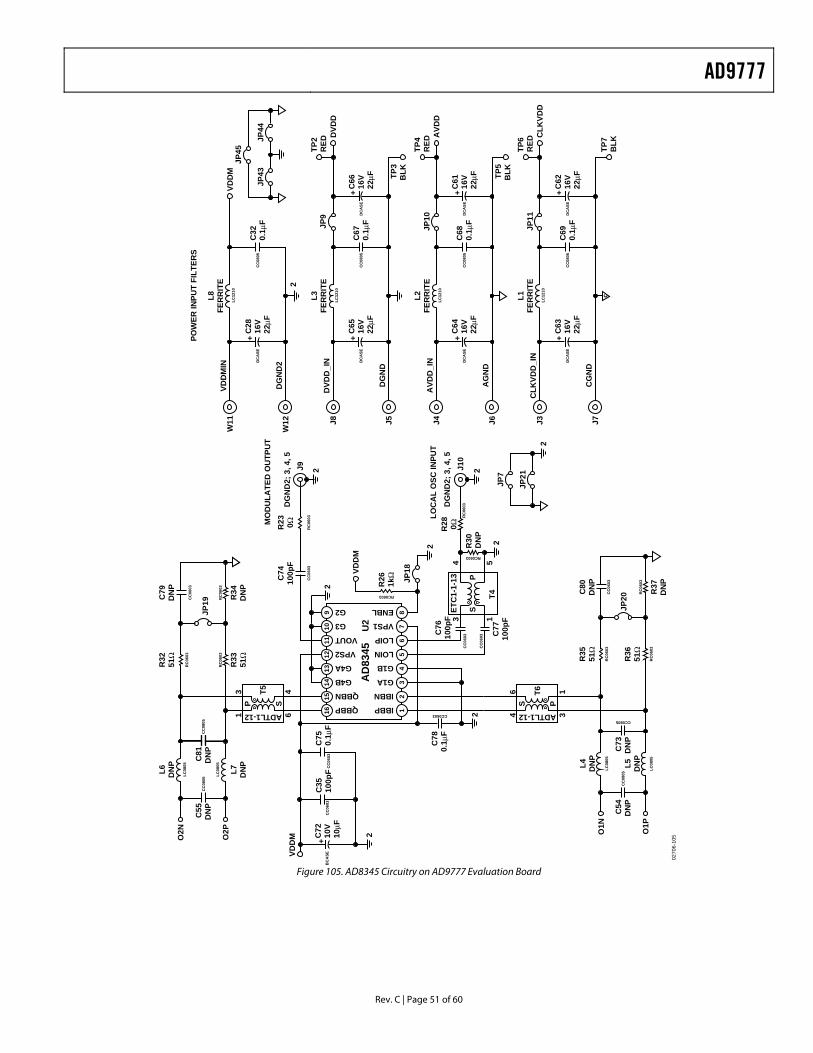
AD9777
Rev. C | Page 51 of 60
JP21
JP7
C54
DN
P
R28 0Ω
R26
1kΩ
R35
51Ω
R36
51Ω
JP20C
79D
NP
R32
51Ω
R34
DN
P
C69
0.1µ
F
C63
16V
22µF
CLK
VDD
_IN
J7
TP6
RED
TP7
BLK
C62
16V
22µF
CLK
VDD
L1FE
RR
ITE
R33
51Ω
C78
0.1µ
F
JP18VD
DM
C72
10V
10µF
C75
0.1µ
F
O2N
O2P O
1N
O1P
JP19
VDD
M
C74
100p
F
C35
100p
F
VDD
M
C76
100p
F
C77
100p
F
R30
DN
P
J10
DG
ND
2; 3
, 4, 5
J9D
GN
D2;
3, 4
, 5
J3
CG
ND
AD
8345
U2
2
2
22
2
RC
0603
RC0603
RC
0603
RC
0603
RC
0603
RC
0603
CC
0603
RC
0603
RC
0603
LC12
10
RC
0603
CC0603
BC
ASE
CC
0603
CC
0603
CC
0603
RC0603
G2 ENBL
VPS1
G1A
G1B
LOIP
VPS2
G4A
G4B
QBBP
VOUT
G3
IBBP
IBBN
LOIN
LOC
AL
OSC
INPU
T
MO
DU
LATE
D O
UTP
UT
POW
ER IN
PUT
FILT
ERS
LC08
05
L6 DN
P
LC08
05
L7 DN
P L4 DN
P
L5 DN
P
JP11
CC
0805
DC
ASE
DC
ASE
CC
0805
T66
ADTL1-12
PS4 3
1
2
2
C80
DN
P
CC
0603
R37
DN
P
C73
DN
P
CC0805
CC
0805
LC08
05
LC08
05
2
CC
0603
QBBN
R23 0Ω
CC
0805
C81
DN
PC
55D
NP
1615
1413
1211
109
12
34
56
78
T45
ETC
1-1-
13
SP
43 1
T53
ADTL1-12
SP1 6
4
CC
0603
JP43
JP45
2
JP44
C68
0.1µ
F
C64
16V
22µF
AVD
D_I
N
J6
TP4
RED
TP5
BLK
C61
16V
22µF
AVD
DJ4
AG
ND
LC12
10
JP10
JP9
CC
0805
DC
ASE
DC
ASE
L2FE
RR
ITE
C67
0.1µ
F
C65
16V
22µF
DVD
D_I
N
J5
TP2
RED
TP3
BLK
C66
16V
22µF
DVD
D
L3FE
RR
ITE
J8
DG
ND
LC12
10
CC
0805
DC
ASE
DC
ASE
C32
0.1µ
F
C28
16V
22µF
VDD
MIN
W12
L8FE
RR
ITE
W11
DG
ND
2
LC12
10
CC
0805
DC
ASE
0270
6-10
5
c
+
+ + + +
+ + +
Figure 105. AD8345 Circuitry on AD9777 Evaluation Board
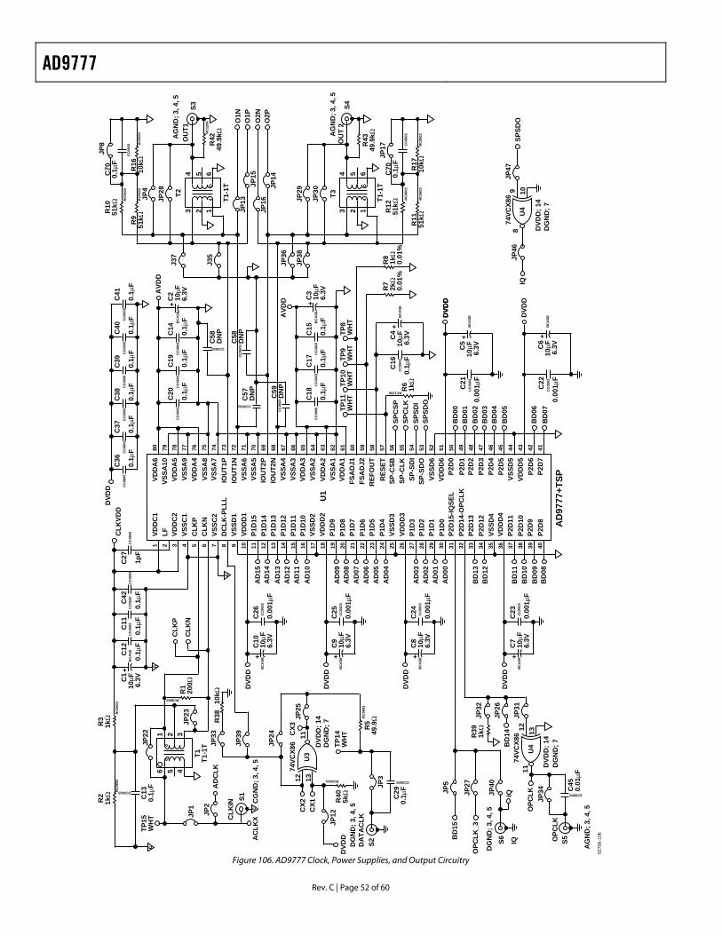
AD9777
Rev. C | Page 52 of 60
1 2 3 4 5 6 7 8 9 10 11 12 13 14 15 16 17 18 19 20 21 22 23 24 25 26 27 28 29 30 31 32 33 34 35 36 37 38 39 40
80 79 78 77 76 75 74 73 72 71 70 69 68 67 66 65 64 63 62 61 60 59 58 57 56 55 54 53 52 51 50 49 48 47 46 45 44 43 42 41
DVD
D
c
c
c
R2
1kΩ
R3
1kΩ
CLK
VDD
DVD
DR
C06
03R
C06
03
BC
ASE
BC
ASE
CC
0603
CC
0603
CC
0603
CC0603
RC0603
TP15
WH
T
T1T1
-1T TP
14W
HT
R1
200Ω
R40
5kΩ
R5
49.9
Ω
R39
1kΩ
C13
0.1µ
F
C1
10µF
6.3V
C10
10µF
6.3V
C26
0.00
1µF
C12
0.1µ
F
C11
0.1µ
F
C42
0.1µ
FC
C06
03C
C08
05C
27 1pF
C36
0.1µ
FCC
0805
C37
0.1µ
FCC
0805
C38
0.1µ
FCC
0805
C39
0.1µ
FCC
0805
C40
0.1µ
FCC
0805
C41
0.1µ
F+
+
cJP
22
JP23
JP33
JP1
CLK
P
CLK
N
R38
10kΩ
JP2
S1
S2 S6
1211
13
IQIQ
S5
U4
AD
CLK
DVD
D
CLK
IN
AC
LKX
CG
ND
; 3, 4
, 5
DG
ND
; 3, 4
, 5D
ATA
CLK
JP39
JP24
JP5
BD
15
BD
14
OPC
LK_3
OPC
LK
74VC
X86
OPC
LK
DG
ND
; 3, 4
, 5
DG
ND
; 7D
VDD
; 14
AG
ND
; 3, 4
, 5
JP27
JP40
JP34
JP32
JP26
JP31
JP3
CX2
74VC
X86
12 1311
U3
DVD
D; 1
4
DVD
D
DG
ND
; 7
CX1
JP25
JP12
CX3
6 5 4
1 2 3
RC
0603
CC
0603
BC
ASE
C9
10µF
6.3V
C25
0.00
1µF
+D
VDD
CC
0603
BC
ASE
C8
10µF
6.3V
C24
0.00
1µF
+D
VDD
CC
0603
BC
ASE
C7
10µF
6.3V
C23
0.00
1µF
+D
VDD
CC
0603
CC0605
CC0805
RC0603
C29
0.1µ
F C45
0.01
µF
AD
15
VDD
C1
VDD
A6
VSSA
10VD
DA
5VS
SA9
VDD
A4
VSSA
8VS
SA7
IOU
T1P
IOU
T1N
VSSA
6VS
SA5
IOU
T2P
IOU
T2N
VSSA
4VS
SA3
VDD
A3
VSSA
2
VSSA
1
VSSD
6VD
DD
6P2
D0
P2D
1P2
D2
P2D
3P2
D4
P2D
5
P2D
6P2
D7
VSSD
5VD
DD
5
VDD
A2
VDD
A1
FSA
DJ1
FSA
DJ2
REF
OU
TR
ESET
SP-C
SBSP
-CLK
SP-S
DI
SP-S
DO
LF VDD
C2
VSSC
1C
LKP
CLK
NVS
SC2
DC
LK-P
LLL
VSSD
1VD
DD
1P1
D15
P1D
14P1
D13
P1D
12P1
D11
P1D
10VS
SD2
VDD
D2
P1D
9P1
D8
P1D
7P1
D6
P1D
5P1
D4
VSSD
3VD
DD
3P1
D3
P1D
2P1
D1
P1D
0P2
D15
-IQSE
LP2
D14
-OPC
LKP2
D13
P2D
12
P2D
11P2
D10
P2D
9P2
D8
VSSD
4VD
DD
4
AD
14A
D13
AD
12A
D11
AD
10
AD
09A
D08
AD
07A
D06
AD
05A
D04
AD
03A
D02
AD
01A
D00
BD
13B
D12
BD
11B
D10
BD
09B
D08
AD
9777
+TSP
U1
C20
0.1µ
FCC
0603
C19
0.1µ
FCC
0603
CC
0603
CC
0603
CC0603
CC0603
RC1206
C14
0.1µ
FBC
ASE
CC
0603
C2
10µF
6.3V
+
C18
0.1µ
F
CC
0603
BC
ASE
C17
0.1µ
F
C16
0.1µ
F
CC
0603
C21
0.00
1µF
CC
0603
CC
0603
C15
0.1µ
FBC
ASE
CC
0805
C3
10µF
6.3V
C4
10µF
6.3V
R7
2kΩ
0.01
%
R8
1kΩ
0.01
%
+
+ BC
ASE
C5
10µF
6.3V
+C58
DN
P
C58
DN
PC
57D
NP
C59
DN
P R6
1kΩ
AVD
D
AVD
D
DVD
D
CC
0603
C22
0.00
1µF
BC
ASE
C6
10µF
6.3V
+
DVD
D
TP11
WH
TTP
10W
HT
TP9
WH
TTP
8W
HT
SPC
SPSP
CLK
SPSD
ISP
SDO
BD
00B
D01
BD
02B
D03
BD
04B
D05
BD
06B
D07
R10
51kΩ
R9
51kΩ
R16
10kΩ
R42
49.9
kΩ
R43
49.9
kΩ
RC
0603
RC
0603
RC
0603
RC
1206
CC
0603
C70
0.1µ
F
JP8
JP4
JP28
JP13
JP15
JP16
JP14
JP36
JP38
JP17
JP29
JP30
AG
ND
; 3, 4
, 5T3
OU
T 2
J37
J35
3T2
S3
O1N
O1P
O2N
O2P
S4
OU
T1A
GN
D; 3
, 4, 5
T1-1
T
2 1
4 5 6
3
T1-1
T
2 1
89 10
4 5 6 C70
0.1µ
FR
1251
kΩ
R11
51kΩ
R17
10kΩ
RC
0603
RC
0603
RC
0603
CC
0603
IQSP
SDO
JP46
JP47
U4
DVD
D; 1
4D
GN
D; 7
74VC
X86
0270
6-10
6
Figure 106. AD9777 Clock, Power Supplies, and Output Circuitry
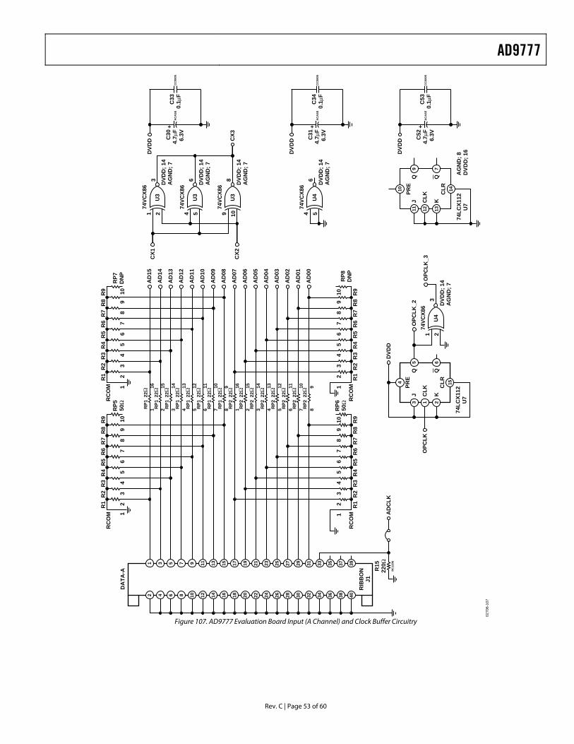
AD9777
Rev. C | Page 53 of 60
0270
6-10
7
J CLK
KC
LR
PRE
74LC
X112
U7
AG
ND
; 8D
VDD
; 16
C52
4.7µ
F6.
3V
DVD
D
C53
0.1µ
FC
C08
05A
CA
SE
1 3 5 7 9 11 13 15 17 19 21 23 25 27 29 31 33 35 37 39
2 4 6 8 10 12 14 16 18 20 22 24 26 28 30 32 34 36 38 40
DA
TA-A
RIB
BO
NJ1
21
34
56
78
910
R1
R2
R3
R4
R5
R6
R7
R8
R9
21
34
56
78
910
R1
R2
R3
R4
R5
R6
R7
R8
R9
RC
OM
RC
OM
RP8
DN
P
RP6 50Ω
21
34
56
78
910
21
34
56
78
910
R1
R2
R3
R4
R5
R6
R7
R8
R9
R1
R2
R3
R4
R5
R6
R7
R8
R9
RC
OM
RC
OM
RP7
DN
PR
P5 50Ω
AD
15
AD
14
AD
13
AD
12
AD
11
AD
10
AD
09
AD
08
AD
07
AD
06
AD
05
AD
04
AD
03
AD
02
AD
01
AD
00
116
215
314
413
512
611
710
89
116
215
314
413
512
611
710
89
RP1
22Ω
RP1
22Ω
RP1
22Ω
RP1
22Ω
RP1
22Ω
RP1
22Ω
RP1
22Ω
RP1
22Ω
RP2
22Ω
RP2
22Ω
RP2
22Ω
RP2
22Ω
RP2
22Ω
RP2
22Ω
RP2
22Ω
RP2
22Ω
R15
220Ω
RC
1206
AD
CLK
74VC
X86
J CLK
KC
LR
PRE
DVD
D
OPC
LK_2 D
VDD
; 14
AG
ND
; 774
LCX1
12U
7
OPC
LK
U4
23
1O
PCLK
_3
3 1 2
5
410 14
11 12 13
9 7
15
6
C31
4.7µ
F6.
3V
DVD
D
C34
0.1µ
FC
C08
05A
CA
SE
C30
4.7µ
F6.
3V
DVD
D
C33
0.1µ
FC
C08
05A
CA
SE
74VC
X86 D
VDD
; 14
AG
ND
; 7
U4
56
4
74VC
X86 D
VDD
; 14
AG
ND
; 7
U3
23
1
74VC
X86 D
VDD
; 14
AG
ND
; 7
U3
56
4
74VC
X86 D
VDD
; 14
AG
ND
; 7
U3
108
9
CX2
CX3
CX1
+ + +
Figure 107. AD9777 Evaluation Board Input (A Channel) and Clock Buffer Circuitry
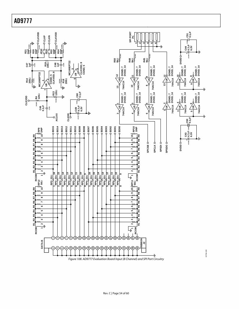
AD9777
Rev. C | Page 54 of 60
0270
6-10
8
1 3 5 7 9 11 13 15 17 19 21 23 25 27 29 31 33 35 37 39
2 4 6 8 10 12 14 16 18 20 22 24 26 28 30 32 34 36 38 40DA
TA-B
RIB
BO
NJ2
21
34
56
78
910
R1
R2
R3
R4
R5
R6
R7
R8
R9
21
34
56
78
910
R1
R2
R3
R4
R5
R6
R7
R8
R9
RC
OM
RC
OM
RP1
0D
NP
RP1
150
Ω
21
34
56
78
910
21
34
56
78
910
R1
R2
R3
R4
R5
R6
R7
R8
R9
R1
R2
R3
R4
R5
R6
R7
R8
R9
RC
OM
RC
OM
RP9
DN
PR
P12
50Ω
BD
15
BD
14
BD
13
BD
12
BD
11
BD
10
BD
09
BD
08
BD
07
BD
06
BD
05
BD
04
BD
03
BD
02
BD
01
BD
00
116
215
314
413
512
611
710
89
116
215
314
413
512
611
710
89
RP3
22Ω
RP3
22Ω
RP3
22Ω
RP3
22Ω
RP3
22Ω
RP3
22Ω
RP3
22Ω
RP3
22Ω
RP4
22Ω
RP4
22Ω
RP4
22Ω
RP4
22Ω
RP4
22Ω
RP4
22Ω
RP4
22Ω
RP4
22Ω
R21
DN
PC
LKVD
D
CG
ND
; 5C
LKVD
D; 8
AC
LKX
R13
120Ω
R4
120Ω
R18
200ΩR14
200Ω
RC
0805
MC
100E
PT22
RC
0805
RC
0805
RC
0805
C43
4.7µ
F6.
3V
DVD
D
C51
0.1µ
F
C44
4.7µ
F6.
3V
DVD
D
DG
ND
; 7D
VDD
; 14
U5
74A
C14
12
DG
ND
; 7D
VDD
; 14
U5
74A
C14
1213
DG
ND
; 7D
VDD
; 14
U5
74A
C14
43
DG
ND
; 7D
VDD
; 14
U5
74A
C14
1011
DG
ND
; 7D
VDD
; 14
U5
74A
C14
65
DG
ND
; 7D
VDD
; 14
U5
74A
C14
89
1 2 3 4 5 6SPI P
OR
TP1
SPC
SB
SPC
LK
SPSD
I
SPSD
OD
GN
D; 7
DVD
D; 1
4
U6
74A
C14
12
DG
ND
; 7D
VDD
; 14
U6
74A
C14
1312
DG
ND
; 7D
VDD
; 14
U6
74A
C14
34
DG
ND
; 7D
VDD
; 14
U6
74A
C14
1110
DG
ND
; 7D
VDD
; 14
U6
74A
C14
56
DG
ND
; 7D
VDD
; 14
U6
74A
C14
98
R50
9kΩ
R48
9kΩ
R45
9kΩ
RC
0805
RC
0805
RC
0805
AC
ASE
CC
805
AC
ASE
C50
0.1µ
FC
C80
5
C60
0.1µ
FC
494.
7µF
6.3V
CLK
DD
AC
ASE
CC
805
436
U8
217
U8
CC
805
C47 1nF
CC
805
JP41
JP42
C46
0.1µ
F
R20
DN
P
RC
0805
R22
DN
P
R24
DN
PRC
0805
RC
0805
RC
0805
CC
805
C48 1nF
CLK
VDD
; 8C
GN
D; 5
MC
100E
PT22
CLK
VDD
CLK
VDD
CLK
N
CLK
P
+ c
c
c
cc
cc
++
R19
100Ω
Figure 108. AD9777 Evaluation Board Input (B Channel) and SPI Port Circuitry
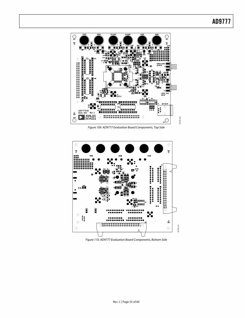
AD9777
Rev. C | Page 55 of 60
0270
6-10
9
Figure 109. AD9777 Evaluation Board Components, Top Side
0270
6-11
0
Figure 110. AD9777 Evaluation Board Components, Bottom Side
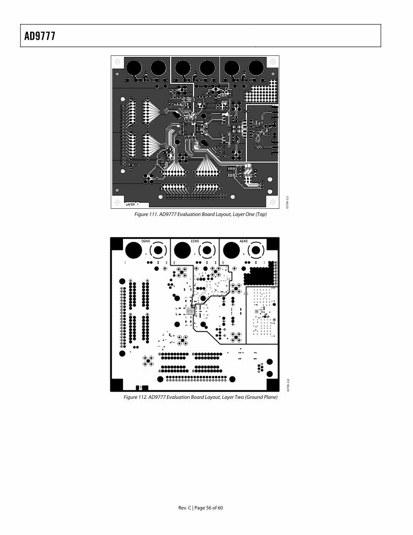
AD9777
Rev. C | Page 56 of 60
0270
6-11
1
Figure 111. AD9777 Evaluation Board Layout, Layer One (Top)
0270
6-11
2
Figure 112. AD9777 Evaluation Board Layout, Layer Two (Ground Plane)
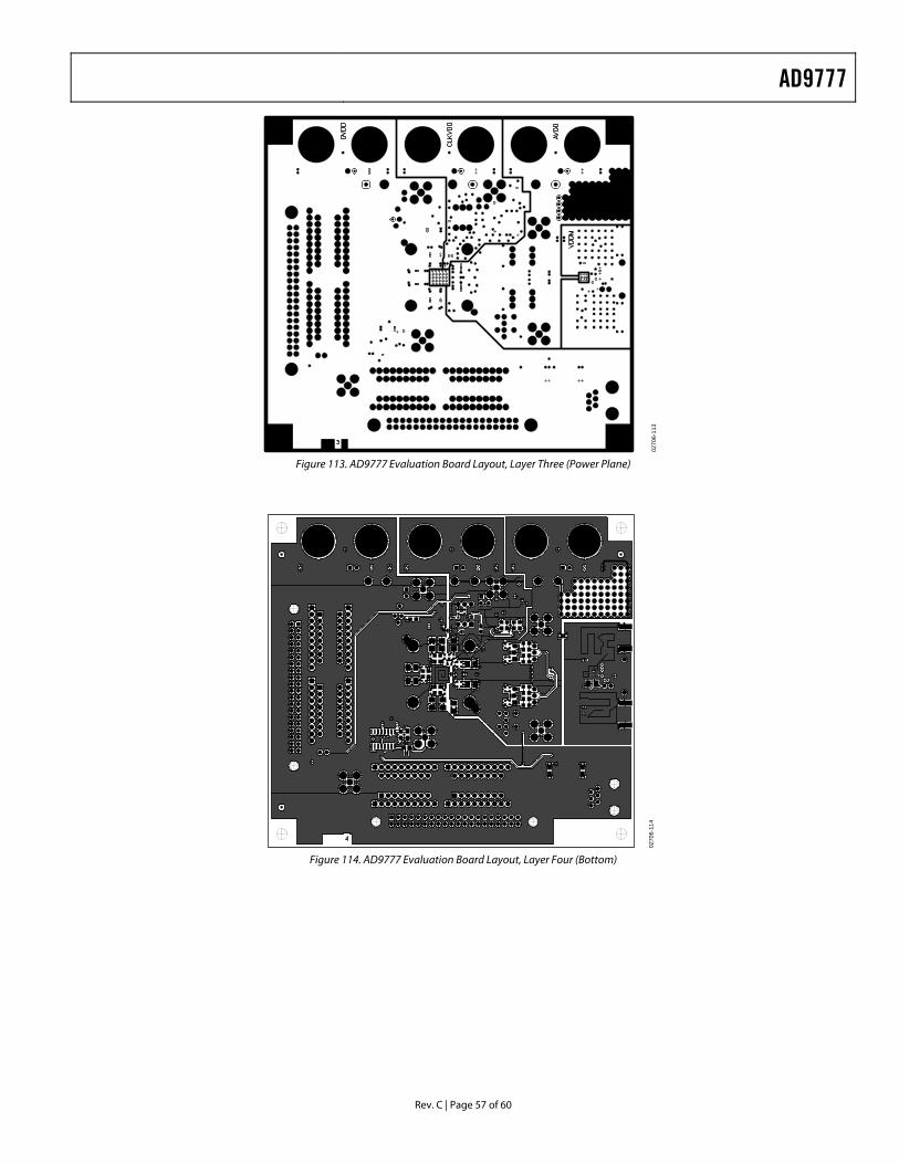
AD9777
Rev. C | Page 57 of 60
0270
6-11
3
Figure 113. AD9777 Evaluation Board Layout, Layer Three (Power Plane)
0270
6-11
4
Figure 114. AD9777 Evaluation Board Layout, Layer Four (Bottom)
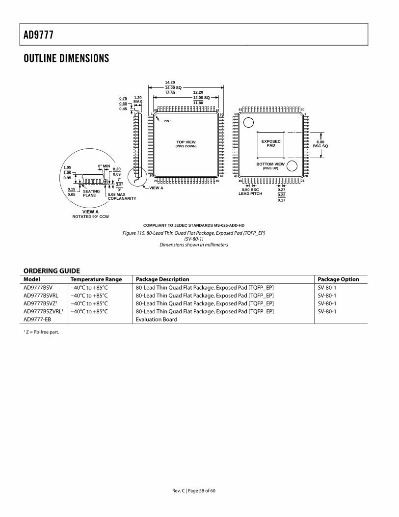
AD9777
Rev. C | Page 58 of 60
OUTLINE DIMENSIONS
COMPLIANT TO JEDEC STANDARDS MS-026-ADD-HD
0.270.220.17
1
20
21 40 40
618060
41
14.2014.00 SQ13.80 12.20
12.00 SQ11.80
0.50 BSCLEAD PITCH
0.750.600.45
1.20MAX
1
2021
61 8060
41
1.051.000.95
0.200.09
0.08 MAXCOPLANARITY
VIEW AROTATED 90° CCW
SEATINGPLANE
0° MIN
7°3.5°0°0.15
0.05VIEW A
PIN 1
TOP VIEW(PINS DOWN)
6.00BSC SQ
BOTTOM VIEW(PINS UP)
EXPOSEDPAD
Figure 115. 80-Lead Thin Quad Flat Package, Exposed Pad [TQFP_EP]
(SV-80-1) Dimensions shown in millimeters
ORDERING GUIDE Model Temperature Range Package Description Package Option AD9777BSV −40°C to +85°C 80-Lead Thin Quad Flat Package, Exposed Pad [TQFP_EP] SV-80-1 AD9777BSVRL −40°C to +85°C 80-Lead Thin Quad Flat Package, Exposed Pad [TQFP_EP] SV-80-1 AD9777BSVZ1 −40°C to +85°C 80-Lead Thin Quad Flat Package, Exposed Pad [TQFP_EP] SV-80-1 AD9777BSZVRL1 −40°C to +85°C 80-Lead Thin Quad Flat Package, Exposed Pad [TQFP_EP] SV-80-1 AD9777-EB Evaluation Board 1 Z = Pb-free part.

AD9777
Rev. C | Page 59 of 60
NOTES

AD9777
Rev. C | Page 60 of 60
© 2005 Analog Devices, Inc. All rights reserved. Trademarks and registered trademarks are the property of their respective owners. C02706-0-1/06(C)
NOTES