TE/MPE/EM/PMT activity Rui de Oliveira on behalf of PCB workshop team 29/11/20121.
Upload
claribel-fisherCategory
view
214download
0
Rui De Oliveira 115/07/2010
Update on large size GEM manufacturing
Rui de Oliveira
Rui De Oliveira 2
Summary
Process Characterization Some pictures Large volume production outside CERN
15/07/2010

Rui De Oliveira 3
GEM single mask process
15/07/2010
Chemical Polyimide etching
Second Polyimide etching
Copper electro etching
Stripping
reality

Rui De Oliveira 415/07/2010
connected Non etched Top Electrode Lower voltage than the Chemical reaction
+3V
Resist layer
+3V 0V
Bath at +3V -everything at ground will be protected -everything at +3V will be chemically etched - An example of active corrosion protection

Starting structure

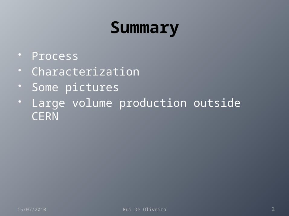
Conventional isotropic metal etching
The hole is created but still an angle in the copper
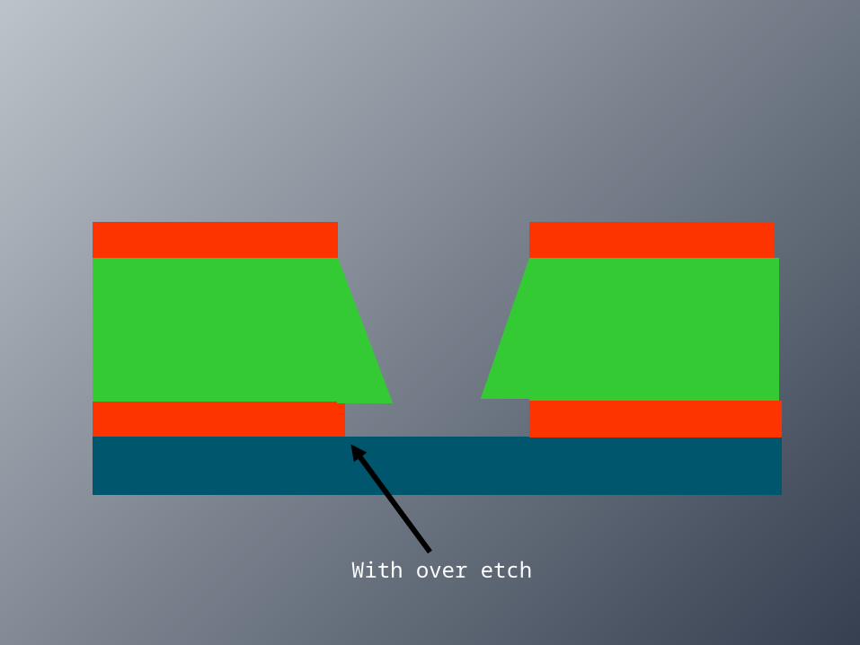
With over etch

Going back to Polyimide etching for 30 secThe hole become bi-conical

Charcaterisation
10
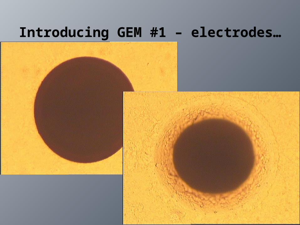
Introducing GEM #1 – electrodes…
11
TOP
BOTTOM
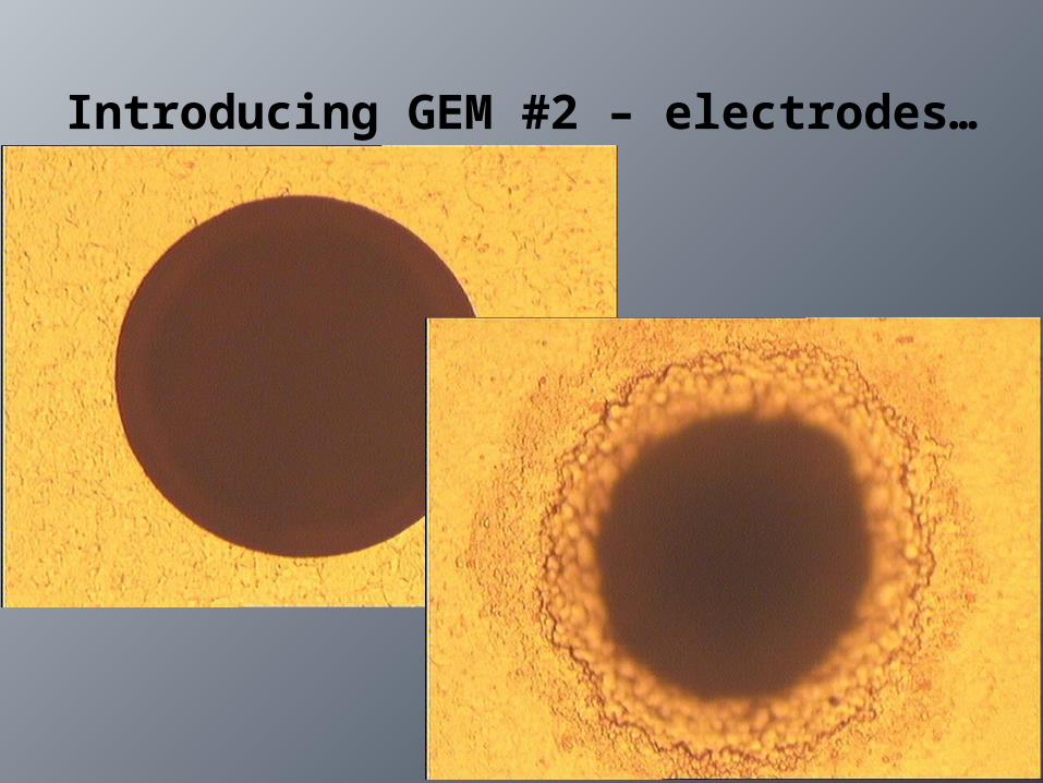
Introducing GEM #2 – electrodes…
12
TOP
BOTTOM

Introducing GEM #3 – electrodes…
13
TOP
BOTTOM
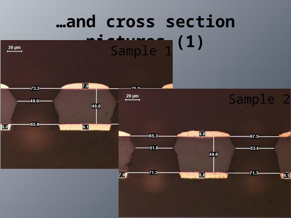
…and cross section pictures (1)
14
TOP
BOTTOM
Sample 1
Sample 2
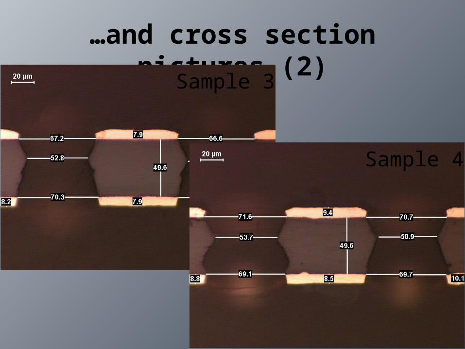
…and cross section pictures (2)
15
TOP
BOTTOM
Sample 3
Sample 4

Preparing the experimental setup
16
Drift
GEM
Anode
3.05 mm
2.15 mm
• GEM active area: 10 x 10 cm2
• Gas mixture: Ar/CO2 70/30• Gas flow: ~ 5 l/h• Water content: ~ 100 ppm H2O• Radiation source: Cu X–ray tube

Taking spectra
17
• Run_0110• Both GEMs in “open–bottom” config• Ed = 2 kV/cm• Ei = 3 kV/cm• DVGEM = 480 V• Energy resolution = 18.4 %
FWHM/peak @ 8.04 keV
• Run_0104• Both GEMs in “open–top” config• Ed = 2 kV/cm• Ei = 3 kV/cm• DVGEM = 480 V• Energy resolution = 19.5 %
FWHM/peak @ 8.04 keV
0 250 500 750 1000 1250
0
100
200
300
400
AD
C c
oun
ts
ADC channel
Run_0104
0 250 500 750 1000 1250
0
100
200
300
400
500
600
700
800
900
1000
1100
1200
1300
1400
AD
C c
oun
ts
ADC channel
Run_0110
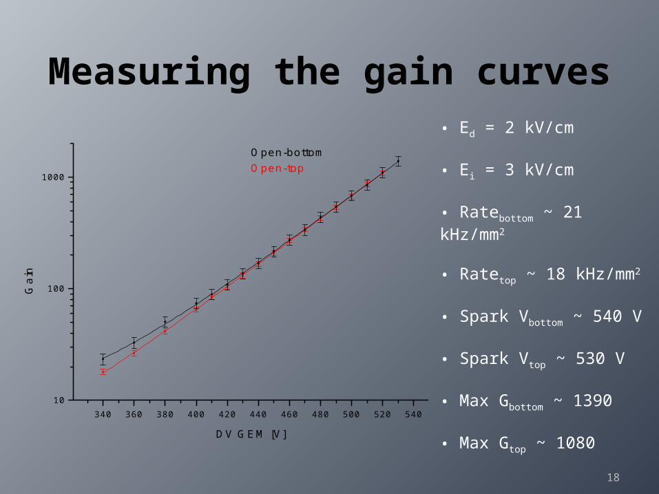
Measuring the gain curves
18
• Ed = 2 kV/cm
• Ei = 3 kV/cm
• Ratebottom ~ 21 kHz/mm2
• Ratetop ~ 18 kHz/mm2
• Spark Vbottom ~ 540 V
• Spark Vtop ~ 530 V
• Max Gbottom ~ 1390
• Max Gtop ~ 1080
340 360 380 400 420 440 460 480 500 520 54010
100
1000
Ga
in
DV GEM [V]
Open-bottomOpen-top

Preparing the experimental setup
19
Drift
GEM3T
Anode
3.25 mm
• GEMs active area: 10 x 10 cm2
• Gas mixture: Ar/CO2 70/30• Gas flow: ~ 5 l/h• Radiation: Ag X–ray tube, Cu filter• 2D (X–Y) readout, all strips shorted• GEMs in open–bottom configuration• HV provided by voltage divider• 2 HV filters on the line (600 k total)
GEM3B
GEM2T
GEM2B
GEM1T
GEM1B
2.215 mm
2.225 mm
2.15 mm

Taking spectra
20
• Ed = 2.09 kV/cm
• DVGEM1 = 391 V
• Et1 = 3.09 kV/cm
• DVGEM2 = 354 V
• Et2 = 3.08 kV/cm
• DVGEM3 = 309 V
• Ei = 3.19 kV/cm
• Rate ~ 2.9 kHz
• Energy resolution=20.6%FWHM/peak @ 8.04 keV
0 250 500 750 1000 1250 1500 1750 2000
0
100
200
300
400
500
600
AD
C c
ou
nts
ADC channel
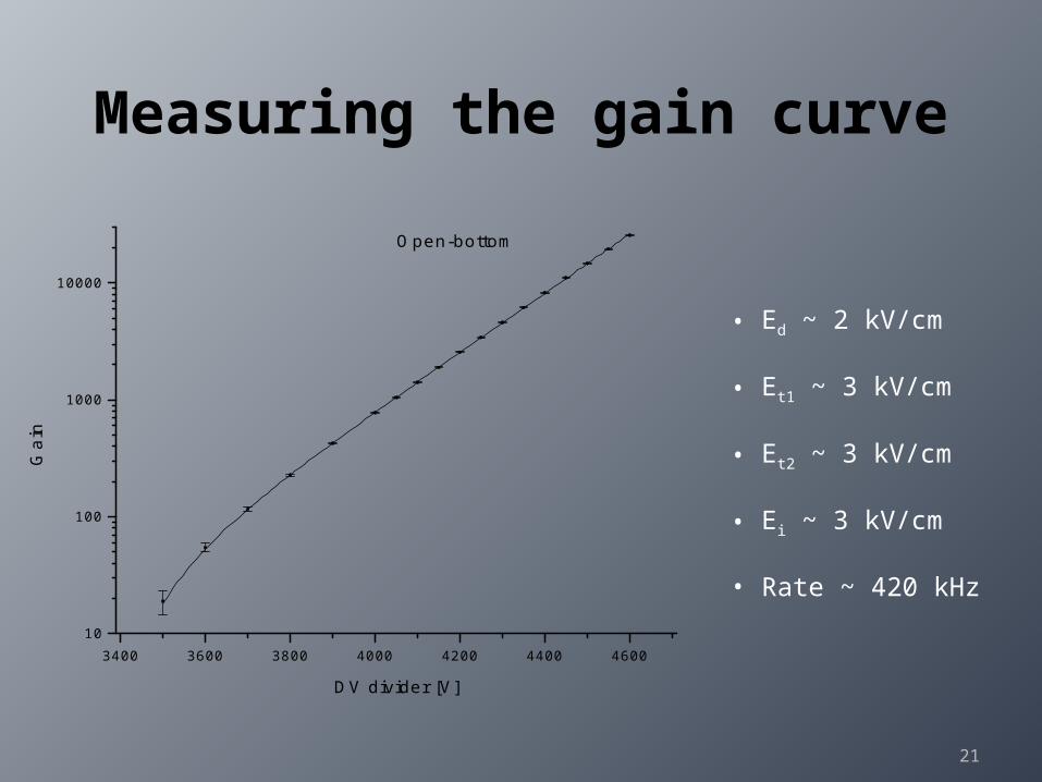
Measuring the gain curve
21
• Ed ~ 2 kV/cm
• Et1 ~ 3 kV/cm
• Et2 ~ 3 kV/cm
• Ei ~ 3 kV/cm
• Rate ~ 420 kHz
3400 3600 3800 4000 4200 4400 460010
100
1000
10000
Open-bottom
Ga
in
DV divider [V]
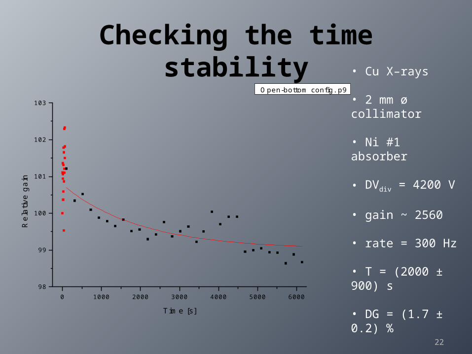
Checking the time stability
22
0 1000 2000 3000 4000 5000 600098
99
100
101
102
103
Open-bottom config. p9
Re
lativ
e g
ain
Time [s]
• Cu X–rays
• 2 mm ø collimator
• Ni #1 absorber
• DVdiv = 4200 V
• gain ~ 2560
• rate = 300 Hz
• T = (2000 ± 900) s
• DG = (1.7 ± 0.2) %

Rui De Oliveira 2415/07/2010

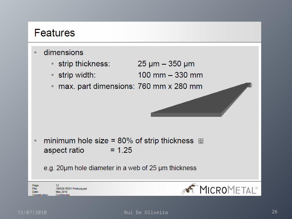
Rui De Oliveira 2515/07/2010
Rui De Oliveira 2615/07/2010