15. Polymer Solar Cells - JKU
86
Adv Polym Sci DOI 10.1007/12_2007_121 © Springer-Verlag Berlin Heidelberg Published online: 17 October 2007 Polymer Solar Cells Harald Hoppe 1 (✉) · N. Serdar Sariciftci 2 1 Institute of Physics, Experimental Physics I, Technical University of Ilmenau, Weimarer Str. 32, 98693 Ilmenau, Germany [email protected] 2 Linz Institute for Organic Solar Cells (LIOS), Physical Chemistry, Johannes Kepler University Linz, Altenbergerstr. 69, 4040 Linz, Austria 1 Introduction 1.1 Basic Working Principles of Polymer Solar Cells 1.2 Device Architectures 1.3 Influence of Electrical Contacts and Open Circuit Voltage 2 Polymer–Fullerene Solar Cells 3 Polymer–Polymer Solar Cells 4 Organic–Inorganic Hybrid Polymer Solar Cells 5 Carbon Nanotubes in Polymer Solar Cells 6 Conclusions and Outlook References Abstract Polymer solar cells, a highly innovative research area for the last decade un- til today, are currently maturing with respect to understanding of their fundamental processes of operation. The increasing interest of the scientific community is well re- flected by the—every year—dynamically rising number of publications. This chapter presents an overview of the developments in organic photovoltaics employing conju- gated polymers as active materials in the photoconversion process. Here the focus is on differentiating between the various material systems applied today: polymer–fullerene, polymer–polymer, polymer–nanoparticle hybrids, and polymer–carbon nanotube combi- nations are reviewed comprehensively. 1 Introduction A polymer solar cell is defined by applying semiconducting conjugated poly- mers [1–3] as active components in the photocurrent generation and power conversion process within thin film photovoltaic devices that convert so- lar light into electrical energy. In the year 2000, Heeger, MacDiarmid, and Shirakawa received the Nobel Prize for Chemistry for the “discovery and de- velopment of conducting polymers”, representing a new class of materials.
Transcript of 15. Polymer Solar Cells - JKU
Adv Polym SciDOI 10.1007/12_2007_121© Springer-Verlag Berlin HeidelbergPublished online: 17 October 2007
Polymer Solar Cells
Harald Hoppe1 (�) · N. Serdar Sariciftci2
1Institute of Physics, Experimental Physics I, Technical University of Ilmenau,Weimarer Str. 32, 98693 Ilmenau, [email protected]
2Linz Institute for Organic Solar Cells (LIOS), Physical Chemistry,Johannes Kepler University Linz, Altenbergerstr. 69, 4040 Linz, Austria
1 Introduction1.1 Basic Working Principles of Polymer Solar Cells1.2 Device Architectures1.3 Influence of Electrical Contacts and Open Circuit Voltage
2 Polymer–Fullerene Solar Cells
3 Polymer–Polymer Solar Cells
4 Organic–Inorganic Hybrid Polymer Solar Cells
5 Carbon Nanotubes in Polymer Solar Cells
6 Conclusions and Outlook
References
Abstract Polymer solar cells, a highly innovative research area for the last decade un-til today, are currently maturing with respect to understanding of their fundamentalprocesses of operation. The increasing interest of the scientific community is well re-flected by the—every year—dynamically rising number of publications. This chapterpresents an overview of the developments in organic photovoltaics employing conju-gated polymers as active materials in the photoconversion process. Here the focus is ondifferentiating between the various material systems applied today: polymer–fullerene,polymer–polymer, polymer–nanoparticle hybrids, and polymer–carbon nanotube combi-nations are reviewed comprehensively.
1Introduction
A polymer solar cell is defined by applying semiconducting conjugated poly-mers [1–3] as active components in the photocurrent generation and powerconversion process within thin film photovoltaic devices that convert so-lar light into electrical energy. In the year 2000, Heeger, MacDiarmid, andShirakawa received the Nobel Prize for Chemistry for the “discovery and de-velopment of conducting polymers”, representing a new class of materials.

H. Hoppe · N.S. Sariciftci
Conducting polymers generally exhibit an alternating single bond–doublebond structure (conjugation) based on sp2-hybridized carbon atoms. Thisleads to a highly delocalized π-electron system with large electronic polar-izability. This enables both absorption within the visible light region, due toπ–π∗ transitions between the bonding and antibonding pz orbitals, and elec-trical charge transport—two requirements that need to be met by semicon-ductors for power generation in solar cells. Using conjugated polymers to fab-ricate optoelectronic devices such as organic light-emitting diodes (OLEDs),organic field-effect transistors (OFETs), and organic solar cells (OSCs) is at-tractive because of their unique processability from solution [4]. Conjugatedpolymers, functionalized by solubilizing side-chain derivations, can be read-ily dissolved in common organic solvents—or even water—and thus can beused as “ink” for all kinds of deposition processes forming thin and homo-geneous films. This property is especially interesting when combined withclassical printing techniques, as it enables both spatially localized deposition(e.g., by inkjet or offset printing) and large area roll-to-roll manufacturing,allowing high-throughput production easily surmounting those achieved byclassical semiconductor batch processing.
Charge carrier mobilities in organic semiconductors are generally muchlower than those of their inorganic counterparts [5]. This disadvantage ispartly balanced by high absorption coefficients [6, 7] and long-lived chargecarriers [8–10], for example in polymer–fullerene blends. Furthermore,recent charge carrier mobilities obtained in polymer [11] and fullerenefilms [12], which are close to or even larger than those obtained in amorphoussilicon films, make them an interesting alternative for, e.g., thin film transistor(TFT) arrays as used in liquid crystal (LCD) or OLED displays.
The structures of several conjugated polymers used in organic solar cells,along with a fullerene, are illustrated in Fig. 1. Three important and com-monly used hole-conducting, donor-type polymers are MDMO-PPV (orOC1C10-PPV) (poly[2-methoxy-5-(3,7-dimethyloctyloxy)]-1,4-phenylene-vinylene), P3HT (poly(3-hexylthiophene-2,5-diyl)), and PFB (poly[9,9′-di-octylfluorene-co-bis-N,N′-(4-butylphenyl)-bis-N,N′-phenyl-1,4-phenylenedi-amine]). Typical electron-conducting acceptors are the polymers CN-MEH-PPV (poly[2-methoxy-5-(2′ -ethylhexyloxy)]-1,4-(1-cyanovinylene)-phenyl-ene) and F8BT (poly(9,9′-dioctylfluorene-co-benzothiadiazole)), and a sol-uble derivative of C60, called PCBM ([6,6]-phenyl C61-butyric acid methylester). All of these materials are solution-processible due to side-chain solu-bilization and the polymers yield strong photo- and electroluminescence.
Conjugated polymers exhibit an alternating single bond–double bondstructure of sp2-hybridized carbon atoms. The electrons in the pz orbitals ofeach sp2-hybridized carbon atom form collectively the π band of the conju-gated polymer. Due to the isomeric effects these π electrons are delocalized,resulting in high electronic polarizability. The Peierls instability splits theoriginally half-filled pz “band” into two, the π and π∗ bands. Upon light ab-

Polymer Solar Cells
Fig. 1 Structures of conjugated polymers and a soluble C60 derivative commonly appliedin polymer-based solar cells
sorption electrons may be excited from the bonding π into the antibondingπ∗ band. This absorption corresponds to the first optical excitation from thehighest occupied molecular orbital (HOMO) to the lowest unoccupied mo-lecular orbital (LUMO). The optical band gaps of most conjugated polymersare around 2 eV.
The portion of the solar light that typical polymeric solar cells absorb islimited. In Fig. 2a the absorption coefficients of thin films from two commonconjugated polymers and PCBM are shown in comparison to the AM 1.5 solar
Fig. 2 Absorption coefficients of two conjugated polymers and a fullerene derivativePCBM, which represent the most often studied polymer–fullerene systems, are showntogether with the AM 1.5 standard solar spectrum
H. Hoppe · N.S. Sariciftci
spectrum. While the silicon band gap and onset of optical absorption spec-trum is around 1.1 eV (ca. 1100 nm), most organic semiconducting polymersused today in photovoltaics utilize only the portion of the solar spectrumbelow 650 nm (larger than ∼2 eV). The absorption coefficients are compara-tively high (∼105 cm–1) and allow for efficient absorption in very thin activelayers.
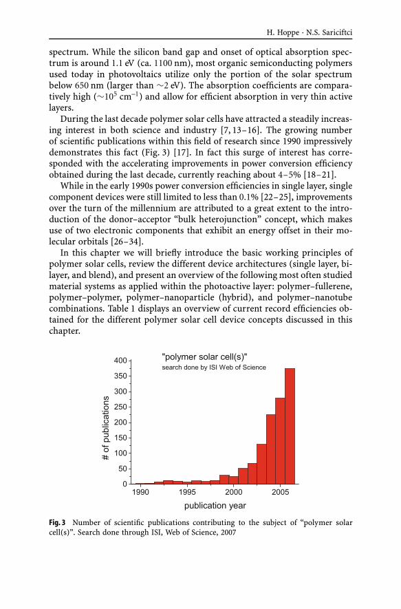
During the last decade polymer solar cells have attracted a steadily increas-ing interest in both science and industry [7, 13–16]. The growing numberof scientific publications within this field of research since 1990 impressivelydemonstrates this fact (Fig. 3) [17]. In fact this surge of interest has corre-sponded with the accelerating improvements in power conversion efficiencyobtained during the last decade, currently reaching about 4–5% [18–21].
While in the early 1990s power conversion efficiencies in single layer, singlecomponent devices were still limited to less than 0.1% [22–25], improvementsover the turn of the millennium are attributed to a great extent to the intro-duction of the donor–acceptor “bulk heterojunction” concept, which makesuse of two electronic components that exhibit an energy offset in their mo-lecular orbitals [26–34].
In this chapter we will briefly introduce the basic working principles ofpolymer solar cells, review the different device architectures (single layer, bi-layer, and blend), and present an overview of the following most often studiedmaterial systems as applied within the photoactive layer: polymer–fullerene,polymer–polymer, polymer–nanoparticle (hybrid), and polymer–nanotubecombinations. Table 1 displays an overview of current record efficiencies ob-tained for the different polymer solar cell device concepts discussed in thischapter.
Fig. 3 Number of scientific publications contributing to the subject of “polymer solarcell(s)”. Search done through ISI, Web of Science, 2007

Polymer Solar Cells
Table 1 Record power conversion efficiencies and device parameters of polymer solar cells
System Materials Refs. Short circuit Open Fill Powercurrent circuit factor conversion
voltage efficiency
Polymer– – a 9.35 mA/cm2 874 mV 64% 5.2%fullerene @ 100 mW
Polymer– F8TBT:P3HT [35] 4 mA/cm2 1250 mV 45% 1.8%b
polymer @ 100 mW
Polymer– P3HT:CdSe [36] 8.79 mA/cm2 620 mV 50% 2.6%b
hybrid nanorods @ 92 mW
Polymer– P3OT:SWCNT [37] 0.5 mA/cm2 750 mV 60% 0.22%nanotube @ 100 mW
a Waldauf C (2007) Device ID: RM8; NREL certified, personal communicationb Corrected for spectral mismatch of the solar simulator
Donor–acceptor diblock copolymers constitute a further interesting classof materials based on the bulk heterojunction concept being developedlately [38–43].
1.1Basic Working Principles of Polymer Solar Cells
Incident light that is absorbed within the photoactive layer of a polymer solarcell leads first to the creation of a bound electron–hole pair—the “exciton”.These excitons diffuse during their lifetime with diffusion lengths generallylimited to about 5–20 nm in organic materials [44–48]. This considerationis important to the design of active layer architectures. If an exciton doesnot eventually separate into its component electron and hole, it eventuallyrecombines by emitting a photon or decaying via thermalization (nonradia-tive recombination). Hence, an exciton dissociation mechanism is required toseparate the excitons which have binding energies ranging between 0.1 and1 eV [49–53]. In single layer organic solar cells this may be achieved by thestrong electric field present within the depletion region of a Schottky con-tact. Exciton dissociation in current polymer solar cells relies on gradients ofthe potential across a donor (D)/acceptor (A) interface, which results in thephotoinduced charge transfer between these materials [26].
Upon light absorption in the donor an electron is excited from the HOMOinto the LUMO. From this excited state the electron may be transferred intothe LUMO of the acceptor. The driving force required for this charge trans-fer is the difference in ionization potential ID∗ of the excited donor and theelectron affinity EA of the acceptor, minus the Coulomb correlations [26]. As

H. Hoppe · N.S. Sariciftci
Fig. 4 Photoinduced charge transfer from a donor (here PPV) to an acceptor (here C60)serves as a highly efficient charge separation mechanism in most polymer solar cells [26]
a result of the photoinduced charge transfer, the positively charged hole re-mains on the donor material whereas the electron is located on the acceptor.This is schematically depicted in Fig. 4 for a soluble derivative of poly(para-phenylenevinylene) as donor and C60 as acceptor.
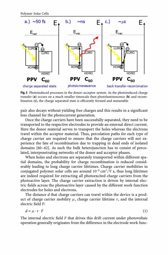
This photoinduced charge transfer between conjugated polymers as donorand fullerenes as acceptor takes place within less than 50 fs [54]. Since allcompeting processes like photoluminescence (∼ns) and back transfer andthus recombination of the charge (∼µs) [8–10] take place on a much largertimescale, the charge separation process is highly efficient and metastable.These possible pathways for the decay of the system after excitation are dis-played in Fig. 5 for comparison.
As a result, the photoinduced charge transfer is accompanied by a strongphotoluminescence quenching of the otherwise highly luminescent conju-gated polymer [26, 55]. In conjugated polymer–fullerene blends, the two signsof charge carriers resulting from exciton dissociation have been clearly iden-tified by means of light-induced electron resonance (LESR) and photoinducedabsorption (PIA) measurements [26].
Recently, geminate polaron pairs have been proposed for polymer–polymer [35, 56, 57] and polymer–fullerene [58, 59] blends as photoinducedintermediates. Here the hole and electron remain coulombically bound acrossthe interface of the donor–acceptor heterojunction. Only via an electric fieldand/or a temperature-assisted secondary process, these geminate polaronpairs are dissociated, leading to free charge carriers. This can have a consider-able effect on the achievable charge separation efficiencies, since the geminate
Polymer Solar Cells
Fig. 5 Photoinduced processes in the donor–acceptor system. As the photoinduced chargetransfer (a) occurs on a much smaller timescale than photoluminescence (b) and recom-bination (c), the charge separated state is efficiently formed and metastable
pair also decays without yielding free charges and this results in a significantloss channel for the photocurrent generation.
Once the charge carriers have been successfully separated, they need to betransported to the respective electrodes to provide an external direct current.Here the donor material serves to transport the holes whereas the electronstravel within the acceptor material. Thus, percolation paths for each type ofcharge carrier are required to ensure that the charge carriers will not ex-perience the fate of recombination due to trapping in dead ends of isolateddomains [60–62]. As such the bulk heterojunction has to consist of perco-lated, interpenetrating networks of the donor and acceptor phases.
When holes and electrons are separately transported within different spa-tial domains, the probability for charge recombination is reduced consid-erably leading to long charge carrier lifetimes. Charge carrier mobilities inconjugated polymer solar cells are around 10–4 cm2/V s, thus long lifetimesare indeed required for extracting all photoexcited charge carriers from thephotoactive layer. The charge carrier extraction is driven by internal elec-tric fields across the photoactive layer caused by the different work functionelectrodes for holes and electrons.
The distance d that charge carriers can travel within the device is a prod-uct of charge carrier mobility µ, charge carrier lifetime τ , and the internalelectric field F:
d = µ · τ ·F (1)
The internal electric field F that drives this drift current under photovoltaicoperation generally originates from the difference in the electrode work func-
H. Hoppe · N.S. Sariciftci
tions. For the example of gold being the hole-accepting (Φ = 5.2 eV) andaluminum being the electron-accepting electrode (Φ = 4.3 eV), an internalelectric field of 105 V/cm is given for an active layer thickness of 90 nm undershort circuit conditions. Assuming charge carrier mobilities of 10–4 cm2/V sand charge carrier lifetimes of 1 µs, a drift length d = 10–4 cm = 100 nm atshort circuit conditions is calculated.
In general the device function of thin organic solar cells, photodiodes, andeven light-emitting diodes can be simplified using the metal–insulator–metal(MIM) model [63]. This is only valid when the organic semiconductors arenot doped and as long as no significant space charge is built up during oper-ation, which would result from unbalanced electron and hole transport.
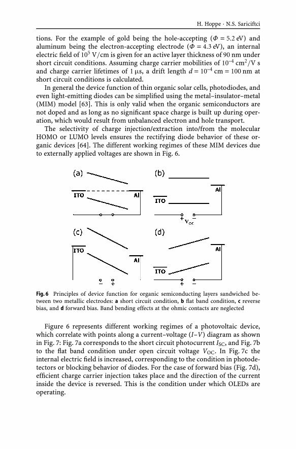
The selectivity of charge injection/extraction into/from the molecularHOMO or LUMO levels ensures the rectifying diode behavior of these or-ganic devices [64]. The different working regimes of these MIM devices dueto externally applied voltages are shown in Fig. 6.
Fig. 6 Principles of device function for organic semiconducting layers sandwiched be-tween two metallic electrodes: a short circuit condition, b flat band condition, c reversebias, and d forward bias. Band bending effects at the ohmic contacts are neglected
Figure 6 represents different working regimes of a photovoltaic device,which correlate with points along a current–voltage (I–V) diagram as shownin Fig. 7: Fig. 7a corresponds to the short circuit photocurrent ISC, and Fig. 7bto the flat band condition under open circuit voltage VOC. In Fig. 7c theinternal electric field is increased, corresponding to the condition in photode-tectors or blocking behavior of diodes. For the case of forward bias (Fig. 7d),efficient charge carrier injection takes place and the direction of the currentinside the device is reversed. This is the condition under which OLEDs areoperating.

Polymer Solar Cells
Fig. 7 Current–voltage characteristics of a polymer solar cell under illumination (solidline) and in the dark (broken line). The various situations (a–d) from Fig. 5 are shownfor comparison
From Fig. 7 the calculation of the power conversion efficiency η can be de-rived: only the fourth quadrant of the I–V curve represents deliverable powerfrom the device. One point on the curve, denoted as maximum power point(MPP), corresponds to the maximum of the product of photocurrent and volt-age and therefore power. The ratio between VMPP · IMPP (or the maximumpower) and VOC · ISC is called the fill factor (FF), and therefore the power out-put is written in the form: Pmax = VOC · ISC ·FF. Division of the output powerby the incident light power res ults in the power conversion efficiency η:
ηPOWER =POUT
PIN=
IMPP VMPP
PIN=
FF ISCVOC
PIN. (2)
As the transport of charges and thus the photocurrent is electric field depen-dent, close to the open circuit voltage the internal electric field is considerablyreduced making the extraction of generated charge carriers less efficient, andleading to limitations in fill factor.
1.2Device Architectures
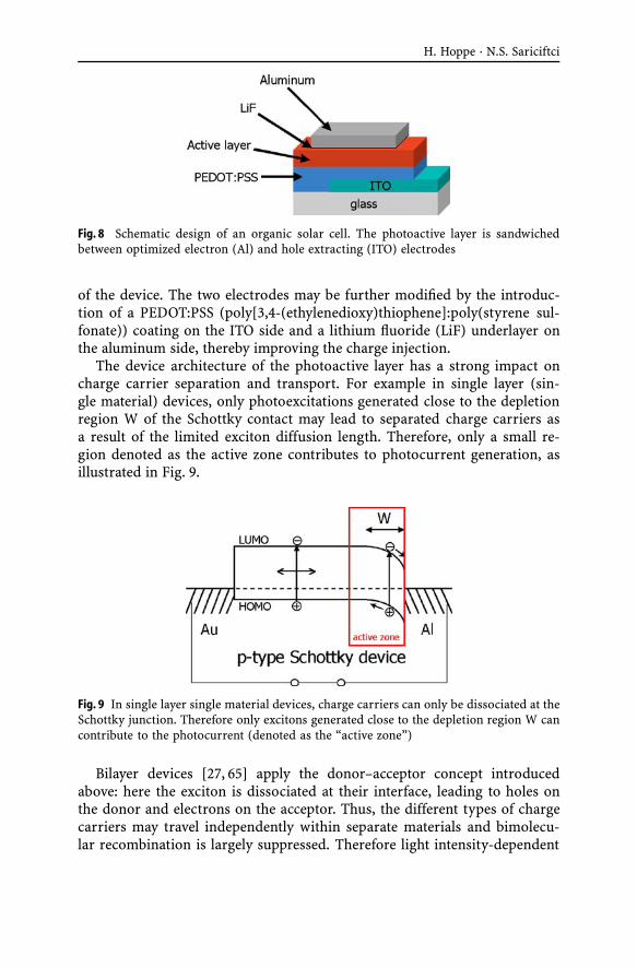
The schematic design of a polymer solar cell is displayed in Fig. 8: the pho-toactive layer is usually sandwiched between an indium tin oxide (ITO)-covered substrate (glass or plastic) and a reflective aluminum back electrode.As the ITO substrate is transparent, illumination takes place from this side
H. Hoppe · N.S. Sariciftci
Fig. 8 Schematic design of an organic solar cell. The photoactive layer is sandwichedbetween optimized electron (Al) and hole extracting (ITO) electrodes
of the device. The two electrodes may be further modified by the introduc-tion of a PEDOT:PSS (poly[3,4-(ethylenedioxy)thiophene]:poly(styrene sul-fonate)) coating on the ITO side and a lithium fluoride (LiF) underlayer onthe aluminum side, thereby improving the charge injection.
The device architecture of the photoactive layer has a strong impact oncharge carrier separation and transport. For example in single layer (sin-gle material) devices, only photoexcitations generated close to the depletionregion W of the Schottky contact may lead to separated charge carriers asa result of the limited exciton diffusion length. Therefore, only a small re-gion denoted as the active zone contributes to photocurrent generation, asillustrated in Fig. 9.
Fig. 9 In single layer single material devices, charge carriers can only be dissociated at theSchottky junction. Therefore only excitons generated close to the depletion region W cancontribute to the photocurrent (denoted as the “active zone”)
Bilayer devices [27, 65] apply the donor–acceptor concept introducedabove: here the exciton is dissociated at their interface, leading to holes onthe donor and electrons on the acceptor. Thus, the different types of chargecarriers may travel independently within separate materials and bimolecu-lar recombination is largely suppressed. Therefore light intensity-dependent

Polymer Solar Cells
photocurrent measurements in these systems exhibited a rather linear behav-ior of the photocurrent with respect to the light intensity, and monomolecularrecombination processes dominate [27, 32, 46]. However, bilayer devices suf-fer also from an active zone limited by the exciton diffusion length, as onlyclose to the geometrical heterojunction photoexcitations can lead to chargecarrier generation, as indicated in Fig. 10.
Fig. 10 In bilayer devices, charge carriers can be dissociated at the donor (D)–accept-or (A) material heterojunction. Only excitons generated within diffusion distance to theinterface can contribute to the photocurrent
This limitation was finally overcome by the concept of the bulk hetero-junction, where the donor and acceptor materials are intimately blendedthroughout the bulk [28–30]. In this way, excitons do not need to travel longdistances to reach the donor/acceptor interface, and charge separation cantake place throughout the whole depth of the photoactive layer. Thus theactive zone extends throughout the volume, as illustrated in Fig. 11. Conse-
Fig. 11 In bulk heterojunction devices, charge carriers can be dissociated throughout thevolume of the active layer. Thus every absorbed photon in the active layer can potentiallycontribute to the photocurrent

H. Hoppe · N.S. Sariciftci
quently the bulk heterojunction concept led to major improvements of thephotocurrent. Today, the bulk heterojunction serves as the state-of-the-artconcept for polymer-based photovoltaics, leading to power conversion effi-ciencies of up to 5% [18–21].
Within the bulk heterojunction, the donor and acceptor domains are gen-erally disordered in volume. For exciton dissociation and charge generationa fine nanoscale intermixing is required, whereas for the efficient transportof charge carriers percolation and a certain phase separation are needed toensure undisturbed transport. Hence the optimization of the nanomorphol-ogy of the photoactive blend is a key issue for improving the efficiency of thephotovoltaic operation [62, 66, 67].
Due to molecular diffusion of fullerenes at elevated temperatures, thephase separation may coarsen with time during operation in full sunlight,representing a morphological instability [68]. To overcome this degrada-tion and for a better control of the nanomorphology itself, several conceptshave been recently introduced to construct ordered bulk heterojunctions.They span a range from using self-assembled inorganic nanostructures forthe infiltration of conjugated polymers [69, 70] up to self-organizing diblockcopolymers [41, 43], where the two blocks carry the different functionalitiesof donor and acceptor, respectively. Figure 12 summarizes the discussed de-vice architectures for comparison.
Fig. 12 Examples of device architectures of conjugated polymer-based photovoltaic cells:a single layer; b bilayer; c “disordered” bulk heterojunction; d ordered bulk heterojunc-tion. (Reproduced with permission from [71], © 2005, American Chemical Society)
1.3Influence of Electrical Contacts and Open Circuit Voltage
The proper choice of metallic contacts in OLEDs was shown to have a majorinfluence on their performance [64]. This was further improved by adjusting
Polymer Solar Cells
the energy barrier height of the hole-injecting anode by interface modifica-tions, like the application of polar self-assembled monolayers (SAMs) [72–75]or the introduction of interlayers using the highly doped polyelectrolyte PE-DOT:PSS [76–79], and by application of lower work function metal cathodesand introduction of thin alkali metal salt interlayers (e.g., LiF) for reducingthe electron injection barrier [80–87]. As a consequence, optimal electro-luminescence quantum efficiencies are achieved when the two conditions,balanced charge carrier injection and balanced charge carrier mobilities, aremet [88].
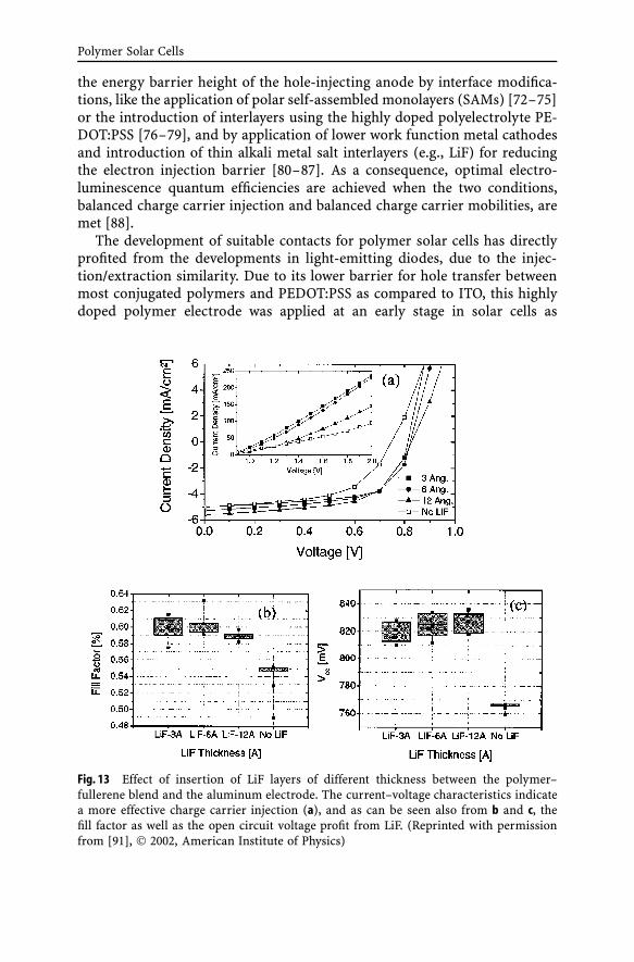
The development of suitable contacts for polymer solar cells has directlyprofited from the developments in light-emitting diodes, due to the injec-tion/extraction similarity. Due to its lower barrier for hole transfer betweenmost conjugated polymers and PEDOT:PSS as compared to ITO, this highlydoped polymer electrode was applied at an early stage in solar cells as
Fig. 13 Effect of insertion of LiF layers of different thickness between the polymer–fullerene blend and the aluminum electrode. The current–voltage characteristics indicatea more effective charge carrier injection (a), and as can be seen also from b and c, thefill factor as well as the open circuit voltage profit from LiF. (Reprinted with permissionfrom [91], © 2002, American Institute of Physics)

H. Hoppe · N.S. Sariciftci
well [13, 32, 89]. Further, the introduction of a LiF underlayer at the alu-minum electrode brought about improvements in open circuit voltage and fillfactor (Fig. 13) [13, 34, 90, 91].
Understanding the effect of this very thin—usually less than a nanometerand up to a few nanometers thick—LiF interlayer has been controversially de-bated. While it was observed that the insertion of the LiF underlayer resultedin an increased built-in potential [92], the mechanism for this effect is notfully clear. One possibility is that LiF leads to the formation of a thin barrier,forming a tunneling junction [80]. However, a thin SiO2 interlayer behavedmuch differently from LiF [91]. As an additional advantage, the formation oftrapping states due to chemical reactions between the aluminum and organicmaterials was prevented by the LiF interlayer [93–95].
Two major effects were proposed as causes for improved electron extrac-tion: (a) upon sublimation of the subsequent aluminum layer the LiF disso-ciates, whereby metallic Li atoms may be formed that consequently n-dopethe organic semiconductor (fullerene or polymer) under formation of Li+
and, e.g., AlF3 [86, 94, 96]; or (b) the LiF layer could result in an interfacialdipole layer shifting the work function of the electrode [82, 90, 91]. Both ofthese viewpoints have been shown to hold merit, as it was demonstratedby photoelectron spectroscopy that for very thin (sub-nanometer) layers ofLiF dissociation and consequent n-type doping occurred, whereas for thickerlayers (a few nanometers) the formation of a dipole was evidenced [97].
In general, the open circuit voltage (VOC) of any solar cell is limited by theenergy difference between the quasi-Fermi level splitting of the free chargecarriers, i.e., the holes and the electrons [98], after their transport through thephotoactive layer and the interfaces at the contacts. While for ideal (ohmic)contacts no energetic loss at the junction is expected, energy level offsets orband bending at non-ideal contacts will further reduce the VOC. Recombina-tion at the electrode may further reduce the quasi-Fermi level splitting.
The charge carriers require a net driving force toward the electrodes,which may in general result from internal electric fields and/or concentrationgradients of the respective charge carrier species. The first leads to a field-induced drift and the other to a diffusion current. Without a detailed analysisone can generally assume that thin film polymer devices (< 100 nm) aremostly field drift dominated whereas thick devices, having effective screen-ing of the electrical fields inside the bulk, are dominated by the diffusionof charge carriers, e.g., by concentration gradients created by the selectivecontacts.
The polaronic level of holes on the conjugated polymer donor phase isslightly above the HOMO of the polymer, and the transport level of theelectrons is closely related to the LUMO level of the acceptor (n-type semi-conductor, e.g., the fullerene). Thus, their resulting energetic splitting has tobe related to the difference between the HOMO of the donor and the LUMOof the acceptor and conceptually determines the maximum open circuit po-

Polymer Solar Cells
tential of the photovoltaic device. This hypothesis has been proven by severalstudies reporting on the variation of the HOMO level of the donor polymer byusing similar compounds with different oxidation potentials [99–102]. Fig-ure 14 displays the linear relationship between the HOMO level of a largerset of conjugated polymers and the open circuit voltage applied in polymer–fullerene bulk heterojunctions.
Fig. 14 Experimentally, a linear relationship between the HOMO level of the conjugatedpolymer (corresponds to onset of oxidation with respect to the Ag/AgCl reference elec-trode) and the measured open circuit voltage (VOC) has been determined for a largenumber of donor polymers. (Reproduced from [102] with permission, © 2006, Wiley-VCH)
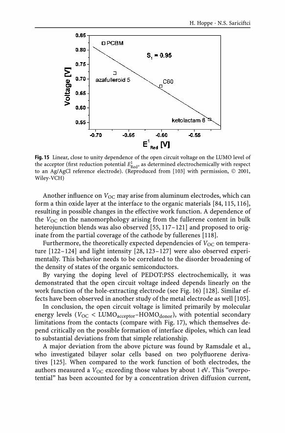
The same linear relationship was already earlier observed for the LUMOlevel of the acceptor fullerene by using fullerene derivatives with different firstreduction potentials (see Fig. 15) [103]. This study has been recently extendedto more fullerenes with smaller electron affinities, confirming this relation-ship [104].
The MIM model predicts the maximum VOC being determined by the dif-ference in the work functions of two asymmetrical electrodes, as long this issmaller than the effective band gap of the insulator [64]. Experimental data,however, showed strong deviations where the VOC exceeded largely the ex-pected difference between the electrode work functions [103]. Fermi levelpinning between the fullerene and the metal electrode has been accounted forthis. In another study, however, deviations from this pinning behavior havebeen found [105]. Thus, the individual energy level alignments between or-ganic/metal interfaces are critical [72, 106–112]. Interfacial dipoles formedat the organic semiconductor/electrode interface change the effective metalwork function and thus affect the VOC as well [72, 108, 109, 113, 114].
H. Hoppe · N.S. Sariciftci
Fig. 15 Linear, close to unity dependence of the open circuit voltage on the LUMO level ofthe acceptor (first reduction potential E1
Red, as determined electrochemically with respectto an Ag/AgCl reference electrode). (Reproduced from [103] with permission, © 2001,Wiley-VCH)
Another influence on VOC may arise from aluminum electrodes, which canform a thin oxide layer at the interface to the organic materials [84, 115, 116],resulting in possible changes in the effective work function. A dependence ofthe VOC on the nanomorphology arising from the fullerene content in bulkheterojunction blends was also observed [55, 117–121] and proposed to orig-inate from the partial coverage of the cathode by fullerenes [118].
Furthermore, the theoretically expected dependencies of VOC on tempera-ture [122–124] and light intensity [28, 123–127] were also observed experi-mentally. This behavior needs to be correlated to the disorder broadening ofthe density of states of the organic semiconductors.
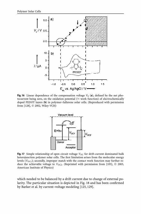
By varying the doping level of PEDOT:PSS electrochemically, it wasdemonstrated that the open circuit voltage indeed depends linearly on thework function of the hole-extracting electrode (see Fig. 16) [128]. Similar ef-fects have been observed in another study of the metal electrode as well [105].
In conclusion, the open circuit voltage is limited primarily by molecularenergy levels (VOC < LUMOacceptor–HOMOdonor), with potential secondarylimitations from the contacts (compare with Fig. 17), which themselves de-pend critically on the possible formation of interface dipoles, which can leadto substantial deviations from that simple relationship.
A major deviation from the above picture was found by Ramsdale et al.,who investigated bilayer solar cells based on two polyfluorene deriva-tives [125]. When compared to the work function of both electrodes, theauthors measured a VOC exceeding those values by about 1 eV. This “overpo-tential” has been accounted for by a concentration driven diffusion current,
Polymer Solar Cells
Fig. 16 Linear dependence of the compensation voltage V0 (a), defined by the net pho-tocurrent being zero, on the oxidation potential (≈ work function) of electrochemicallydoped PEDOT layers (b) in polymer–fullerene solar cells. (Reproduced with permissionfrom [128], © 2002, Wiley-VCH)
Fig. 17 Simple relationship of open circuit voltage VOC for drift-current dominated bulkheterojunction polymer solar cells. The first limitation arises from the molecular energylevels (VOC1); secondly, improper match with the contact work function may further re-duce the achievable voltage to VOC2. (Reprinted with permission from [105], © 2003,American Institute of Physics)
which needed to be balanced by a drift current due to change of external po-larity. The particular situation is depicted in Fig. 18 and has been confirmedby Barker et al. by current–voltage modeling [125, 129].

H. Hoppe · N.S. Sariciftci
Fig. 18 Situation for a bilayer device, where the open circuit voltage exceeds the workfunction difference considerably by 1 V due to a concentration driven diffusion current.(Reprinted with permission from [125], © 2002, American Institute of Physics)
2Polymer–Fullerene Solar Cells
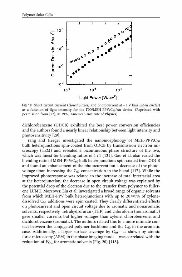
Since the discovery of photoinduced charge transfer from a conjugatedpolymer (MEH-PPV) to a buckminsterfullerene (C60) in 1992 by Sariciftciet al. [26], a dynamic development of solar cell devices exploiting this effecthas followed. First applications of these two materials in bilayer geometryresulted in short circuit photocurrents following linearly the incident lightintensity, even at higher illumination densities (Fig. 19) [27].
This linear dependence has been confirmed by Halls et al. using the samebilayer structure but employing PPV as the electron donor [44]. The authorsestimated the exciton diffusion length of PPV to be in the range of 6–8 nmfrom both the spectral response and the absolute efficiency [44]. Later Romanet al. demonstrated optical modeling to be a useful tool for the optimizationof such bilayer solar cells, which in their case was based on a polythio-phene derivative and C60 [89]. The optical modeling was detailed by Pettersonet al. [46].
In a next step of development a side group was attached to the C60 to al-low for solution processing due to increased solubility in common organicsolvents [130]. PCBM provides the best performances in polymer–fullerenesolar cells, even to date. The first bulk heterojunction polymer solar cellswere based on MEH-PPV and PCBM, and were presented by Yu et al. [29].In these bulk heterojunctions, an intimate blending of the donor and ac-ceptor components results in a very efficient exciton dissociation and thuscharge carrier generation throughout the whole volume of the blend. MEH-PPV:PCBM blends with a mixing ratio of 1 : 4 spin-coated from ortho-1,2-
Polymer Solar Cells
Fig. 19 Short circuit current (closed circles) and photocurrent at – 1 V bias (open circles)as a function of light intensity for the ITO/MEH-PPV/C60/Au device. (Reprinted withpermission from [27], © 1992, American Institute of Physics)
dichlorobenzene (ODCB) exhibited the best power conversion efficienciesand the authors found a nearly linear relationship between light intensity andphotosensitivity [29].
Yang and Heeger investigated the nanomorphology of MEH-PPV:C60bulk heterojunctions spin-coated from ODCB by transmission electron mi-croscopy (TEM) and revealed a bicontinuous phase structure of the two,which was finest for blending ratios of 1 : 1 [131]. Gao et al. also varied theblending ratio of MEH-PPV:C60 bulk heterojunctions spin-coated from ODCBand found an enhancement of the photocurrent but a decrease of the photo-voltage upon increasing the C60 concentration in the blend [117]. While theimproved photoresponse was related to the increase of total interfacial areaat the heterojunction, the decrease in open circuit voltage was explained bythe potential drop of the electron due to the transfer from polymer to fuller-ene LUMO. Moreover, Liu et al. investigated a broad range of organic solventsfrom which MEH-PPV bulk heterojunctions with up to 20 wt % of xylene-dissolved C60 additions were spin coated. They clearly differentiated effectson photocurrent and open circuit voltage due to aromatic and nonaromaticsolvents, respectively. Tetrahydrofuran (THF) and chloroform (nonaromatic)gave smaller currents but higher voltages than xylene, chlorobenzene, anddichlorobenzene (aromatic). The authors related this to a more intimate con-tact between the conjugated polymer backbone and the C60 in the aromaticcase. Additionally, a larger surface coverage by C60—as shown by atomicforce microscopy (AFM) in the phase imaging mode—was correlated with thereduction of VOC for aromatic solvents (Fig. 20) [118].
H. Hoppe · N.S. Sariciftci
Fig. 20 �AFM micrographs (both height image and phase image) of MEH-PPV/C60(20 wt %) composite films fabricated with a xylene, b DCB, and c THF. The phase imageenables calculation of the C60 surface coverage. (Reproduced from [118] with permission,© 2001, Wiley-VCH)
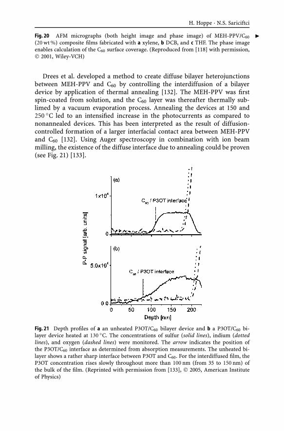
Drees et al. developed a method to create diffuse bilayer heterojunctionsbetween MEH-PPV and C60 by controlling the interdiffusion of a bilayerdevice by application of thermal annealing [132]. The MEH-PPV was firstspin-coated from solution, and the C60 layer was thereafter thermally sub-limed by a vacuum evaporation process. Annealing the devices at 150 and250 ◦C led to an intensified increase in the photocurrents as compared tononannealed devices. This has been interpreted as the result of diffusion-controlled formation of a larger interfacial contact area between MEH-PPVand C60 [132]. Using Auger spectroscopy in combination with ion beammilling, the existence of the diffuse interface due to annealing could be proven(see Fig. 21) [133].
Fig. 21 Depth profiles of a an unheated P3OT/C60 bilayer device and b a P3OT/C60 bi-layer device heated at 130 ◦C. The concentrations of sulfur (solid lines), indium (dottedlines), and oxygen (dashed lines) were monitored. The arrow indicates the position ofthe P3OT/C60 interface as determined from absorption measurements. The unheated bi-layer shows a rather sharp interface between P3OT and C60. For the interdiffused film, theP3OT concentration rises slowly throughout more than 100 nm (from 35 to 150 nm) ofthe bulk of the film. (Reprinted with permission from [133], © 2005, American Instituteof Physics)

Polymer Solar Cells
H. Hoppe · N.S. Sariciftci
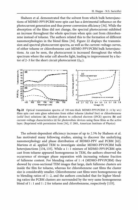
Shaheen et al. demonstrated that the solvent from which bulk heterojunc-tions of MDMO-PPV:PCBM were spin cast has a detrimental influence on thephotocurrent generation and thus power conversion efficiency [34]. While theabsorption of the films did not change, the spectral photocurrent exhibitedan increase throughout the whole spectrum when spin cast from chloroben-zene instead of toluene. The authors related this to the formation of differentnanomorphologies in the blend films [34]. Figure 22 displays the transmis-sion and spectral photocurrent spectra, as well as the current–voltage curves,of either toluene or chlorobenzene cast MDMO-PPV:PCBM bulk heterojunc-tions. As can be seen, the photocurrent is increased throughout the wholespectrum where the solar cell absorbs light, leading to improvement by a fac-tor of 2–3 for the short circuit photocurrent (ISC).
Fig. 22 Optical transmission spectra of 100-nm-thick MDMO-PPV:PCBM (1 : 4 by wt.)films spin cast onto glass substrates from either toluene (dashed line) or chlorobenzene(solid line) solutions (a). Incident photon to collected electron (IPCE) spectra (b) andcurrent–voltage characteristics (c) for photovoltaic devices using these films as the activelayer. (Reprinted with permission from [34], © 2001, American Institute of Physics)
The solvent-dependent efficiency increase of up to 2.5% by Shaheen et al.has motivated many following studies, aiming to discover the underlyingnanomorphology and phase distribution of MDMO-PPV and PCBM [62].Martens et al. applied TEM to investigate similar MDMO-PPV:PCBM bulkheterojunctions [134, 135]. While a 1 : 1 mixture of MDMO-PPV:PCBM spincast from toluene appeared homogeneous in TEM, the authors observed theoccurrence of stronger phase separation with increasing volume fractionof fullerene content. For blending ratios of 1 : 4 (MDMO-PPV:PCBM) theyshowed by cross-sectional TEM images that large, dark fullerene clusters areinside the film for toluene, whereas for chlorobenzene cast films the clustersize is considerably smaller. Chlorobenzene cast films were homogeneous upto blending ratios of 1 : 2, and the authors concluded that for higher blend-ing ratios the PCBM clusters are surrounded by the very same homogeneousblend of 1 : 1 and 1 : 2 for toluene and chlorobenzene, respectively [135].
Polymer Solar Cells
Furthermore, Martens et al. have shown by AFM that the drying time is animportant parameter for the size of the phase-separated structures. By intro-ducing a hot air flow over a drying film, the drying time could be decreasedand consequently the extent of phase separation was reduced [136].
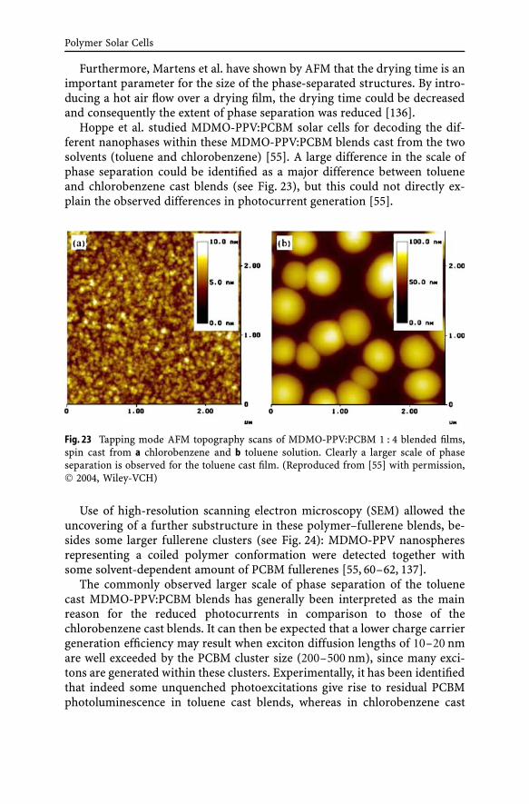
Hoppe et al. studied MDMO-PPV:PCBM solar cells for decoding the dif-ferent nanophases within these MDMO-PPV:PCBM blends cast from the twosolvents (toluene and chlorobenzene) [55]. A large difference in the scale ofphase separation could be identified as a major difference between tolueneand chlorobenzene cast blends (see Fig. 23), but this could not directly ex-plain the observed differences in photocurrent generation [55].
Fig. 23 Tapping mode AFM topography scans of MDMO-PPV:PCBM 1 : 4 blended films,spin cast from a chlorobenzene and b toluene solution. Clearly a larger scale of phaseseparation is observed for the toluene cast film. (Reproduced from [55] with permission,© 2004, Wiley-VCH)
Use of high-resolution scanning electron microscopy (SEM) allowed theuncovering of a further substructure in these polymer–fullerene blends, be-sides some larger fullerene clusters (see Fig. 24): MDMO-PPV nanospheresrepresenting a coiled polymer conformation were detected together withsome solvent-dependent amount of PCBM fullerenes [55, 60–62, 137].
The commonly observed larger scale of phase separation of the toluenecast MDMO-PPV:PCBM blends has generally been interpreted as the mainreason for the reduced photocurrents in comparison to those of thechlorobenzene cast blends. It can then be expected that a lower charge carriergeneration efficiency may result when exciton diffusion lengths of 10–20 nmare well exceeded by the PCBM cluster size (200–500 nm), since many exci-tons are generated within these clusters. Experimentally, it has been identifiedthat indeed some unquenched photoexcitations give rise to residual PCBMphotoluminescence in toluene cast blends, whereas in chlorobenzene cast

H. Hoppe · N.S. Sariciftci
Fig. 24 SEM cross sections of chlorobenzene (a, b) and toluene (c, d) based MDMO-PPV:PCBM blends. Whereas chlorobenzene based blends are rather homogeneous,toluene cast blends reveal large PCBM clusters embedded in a polymer-rich matrix orskin layer. Small features—referred to as “nanospheres”—are visible in all cases and canbe attributed to the polymer in a coiled conformation. The blending ratio is depicted inthe lower right corner. (Reproduced from [55] with permission, © 2004, Wiley-VCH)
blends the fullerene photoluminescence could not be detected any more [55].However, since the spectral photocurrent data show a vital contribution fromthe fullerene also in the case of toluene cast blends, the photocurrent in theregion of the large fullerene cluster may have a significant contribution fromdark triplet excitons that exhibit a longer lifetime and thus may diffuse longerdistances—long enough to reach the heterojunction interface [62, 126].
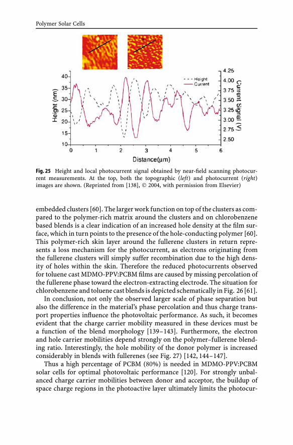
Deeper insight can be gained from a scanning near-field optical mi-croscopy (SNOM) study by McNeill et al., who resolved the local photocurrentobtained on MDMO-PPV:PCBM toluene cast blends [138]. The authors re-vealed that the photocurrent was considerably reduced on top of the smallhills caused by the PCBM clusters (Fig. 25), whereas it stayed nearly constantover the surface of chlorobenzene cast blends [138].
As could already be inferred from the cross-sectional SEM images, the ful-lerene clusters are in fact surrounded by a polymer-rich skin layer [55, 60].Using Kelvin probe force microscopy Hoppe et al. were able to confirm this bythe detection of a considerably increased work function on top of the polymer
Polymer Solar Cells
Fig. 25 Height and local photocurrent signal obtained by near-field scanning photocur-rent measurements. At the top, both the topographic (left) and photocurrent (right)images are shown. (Reprinted from [138], © 2004, with permission from Elsevier)
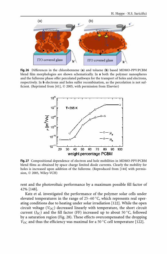
embedded clusters [60]. The larger work function on top of the clusters as com-pared to the polymer-rich matrix around the clusters and on chlorobenzenebased blends is a clear indication of an increased hole density at the film sur-face, which in turn points to the presence of the hole-conducting polymer [60].This polymer-rich skin layer around the fullerene clusters in return repre-sents a loss mechanism for the photocurrent, as electrons originating fromthe fullerene clusters will simply suffer recombination due to the high dens-ity of holes within the skin. Therefore the reduced photocurrents observedfor toluene cast MDMO-PPV:PCBM films are caused by missing percolation ofthe fullerene phase toward the electron-extracting electrode. The situation forchlorobenzene and toluene cast blends is depicted schematically in Fig. 26 [61].
In conclusion, not only the observed larger scale of phase separation butalso the difference in the material’s phase percolation and thus charge trans-port properties influence the photovoltaic performance. As such, it becomesevident that the charge carrier mobility measured in these devices must bea function of the blend morphology [139–143]. Furthermore, the electronand hole carrier mobilities depend strongly on the polymer–fullerene blend-ing ratio. Interestingly, the hole mobility of the donor polymer is increasedconsiderably in blends with fullerenes (see Fig. 27) [142, 144–147].
Thus a high percentage of PCBM (80%) is needed in MDMO-PPV:PCBMsolar cells for optimal photovoltaic performance [120]. For strongly unbal-anced charge carrier mobilities between donor and acceptor, the buildup ofspace charge regions in the photoactive layer ultimately limits the photocur-
H. Hoppe · N.S. Sariciftci
Fig. 26 Differences in the chlorobenzene (a) and toluene (b) based MDMO-PPV:PCBMblend film morphologies are shown schematically. In a both the polymer nanospheresand the fullerene phase offer percolated pathways for the transport of holes and electrons,respectively. In b electrons and holes suffer recombination, as the percolation is not suf-ficient. (Reprinted from [61], © 2005, with permission from Elsevier)
Fig. 27 Compositional dependence of electron and hole mobilities in MDMO-PPV:PCBMblend films as obtained by space charge limited diode currents. Clearly the mobility forholes is increased upon addition of the fullerene. (Reproduced from [144] with permis-sion, © 2005, Wiley-VCH)
rent and the photovoltaic performance by a maximum possible fill factor of42% [148].
Katz et al. investigated the performance of the polymer solar cells underelevated temperatures in the range of 25–60 ◦C, which represents real oper-ating conditions due to heating under solar irradiation [122]. While the opencircuit voltage (VOC) decreased linearly with temperature, the short circuitcurrent (ISC) and the fill factor (FF) increased up to about 50 ◦C, followedby a saturation region (Fig. 28). These effects overcompensated the droppingVOC and thus the efficiency was maximal for a 50 ◦C cell temperature [122].

Polymer Solar Cells
Fig. 28 Solar cell parameters for MDMO-PPV:PCBM polymer solar cells under slightlyelevated temperatures, as expected for realistic operation conditions. Interestingly, theshort circuit photocurrent increases with temperature, while the open circuit voltagedrops. As a result the power conversion efficiency is maximized for temperatures of 50 ◦C.(Reprinted with permission from [122], © 2001, American Institute of Physics)
The increase of ISC and FF were attributed to a temperature-activatedhopping charge transport in disordered organic semiconductors (comparewith [149]). Further studies were extended to low temperatures and con-firmed the temperature-dependent behavior of the solar cell parameters,resulting in specific activation energies for the thermally activated chargetransport [123, 124, 150, 151]. At low temperatures the open circuit voltagesaturates. Riedel et al. also investigated the illumination dependence of ISC,VOC, and FF [151]. Higher light intensities generally lead to increased opencircuit voltages but decreased fill factors and power conversion efficiencies.Interestingly, the parallel or shunt resistance RP was found to decrease forlarger light intensities [151].
Mihailetchi et al. described the electric field-dependent photocurrent inpolymer–fullerene bulk heterojunctions by solving the Poisson and continu-ity equations, taking geminate polaron pair formation and dissociation intoaccount [58]. It was postulated that after the photoinduced charge transferprocess, the hole and electron still remain coulombically bound to each otheracross the heterojunction (geminate polaron pair), and that the field- andtemperature-dependent dissociation of these electron–hole pairs is describedby a Braun-modified Onsager’s theory of ion pair dissociation [58, 152, 153].Koster et al. presented a numerical model including the effects of recombina-tion and space-charge along with the parameters used for fitting the data ofMDMO-PPV:PCBM based solar cells [59]. Figure 29 shows the photocurrent
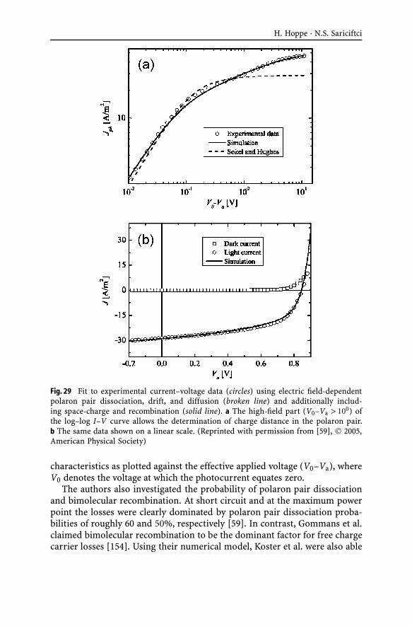
H. Hoppe · N.S. Sariciftci
Fig. 29 Fit to experimental current–voltage data (circles) using electric field-dependentpolaron pair dissociation, drift, and diffusion (broken line) and additionally includ-ing space-charge and recombination (solid line). a The high-field part (V0–Va > 100) ofthe log–log I–V curve allows the determination of charge distance in the polaron pair.b The same data shown on a linear scale. (Reprinted with permission from [59], © 2005,American Physical Society)
characteristics as plotted against the effective applied voltage (V0–Va), whereV0 denotes the voltage at which the photocurrent equates zero.
The authors also investigated the probability of polaron pair dissociationand bimolecular recombination. At short circuit and at the maximum powerpoint the losses were clearly dominated by polaron pair dissociation proba-bilities of roughly 60 and 50%, respectively [59]. In contrast, Gommans et al.claimed bimolecular recombination to be the dominant factor for free chargecarrier losses [154]. Using their numerical model, Koster et al. were also able
Polymer Solar Cells
to describe accurately the light intensity dependence of both the open cir-cuit voltage and the short circuit photocurrent for polymer–fullerene solarcells [155, 156].
In contrast, Schilinsky et al. and Waldauf et al. used an extended numer-ical description according to the p–n junction model and demonstrated aswell a proper description of light intensity-dependent device current–voltagecharacteristics [127, 157, 158]. Thus, several numerical models for the elec-trical description of polymer–fullerene photovoltaic devices have been pre-sented in the literature to date, and there is an ongoing discussion in thescientific community about them.
For an adequate understanding of the photogeneration process in thesethin film multilayer solar cells, optical modeling of light propagation and ab-sorption is required. Due to the thin film thickness for most of the layers inthe device, coherent light propagation needs to be considered to take possibleinterference effects properly into account. The commonly applied numeri-cal description is done by the so-called transfer matrix formalism [159]. Theresulting generation density of excitons can then be used as input for theelectrical description of the device. Optical modeling has been done for bothbilayers [46, 160, 161] and bulk heterojunction [6, 162–166] solar cells.
Synthesis via the “sulfinyl route” led to a reduced number of defects onthe MDMO-PPV donor polymer and showed some improved performancesin MDMO-PPV:PCBM bulk heterojunctions [167, 168]. The lower defect dens-ity resulted in a more regioregular (head-to-tail) order within the MDMO-PPV, leading to charge carrier mobility improvements and ultimately to animproved efficiency of 2.65% for MDMO-PPV:PCBM based bulk heterojunc-tions [169]. This was accompanied by a fill factor of 71% [169], which to datehas not been exceeded by any other polymer solar cell device.
A further improvement of MDMO-PPV based bulk heterojunctions wasachieved by the application of a new C70 fullerene derivative, which wassubstituted with the same side chains as PCBM and is therefore called[70]PCBM [170]. Due to the reduced symmetry of C70 as compared tothe football sphere (icosahedral symmetry) of C60, more optical transitionsare allowed and thus the visible light absorption is considerably increasedfor [70]PCBM. This led to an improved external quantum efficiency (EQE) ofMDMO-PPV based solar cells reaching up to 66% (Fig. 30). As a result thepower conversion efficiency was boosted to 3% under AM 1.5 solar simula-tion at 1000 W/m2 [170].
Thermally activated PCBM diffusion and formation of crystalline aggre-gates within blends with PPV derivatives were observed even at moder-ate temperatures [55, 68, 137]. In contrast, polythiophene based polymer–fullerene solar cells had an overall performance improvement upon thermalannealing steps [171, 172]. This improvement has been mainly correlatedwith an improved order in the film. This is especially true in the case ofpolythiophene, which is known to convert to a more ordered phase upon

H. Hoppe · N.S. Sariciftci
Fig. 30 Photovoltaic properties of an MDMO-PPV based polymer–fullerene solar cell withan active area of 0.1 cm2. a External quantum efficiency (EQE) of [70]PCBM:MDMO-PPV cells, spin-coated from chlorobenzene (triangles) and ODCB (squares), andof [60]PCBM:MDMO-PPV devices spin-coated from chlorobenzene (open circles);b current–voltage characteristics of [70]PCBM:MDMO-PPV devices, spin-coated fromODCB in the dark (open circles) and under illumination (AM 1.5, 1000 W/m2; squares).The inset shows the I–V characteristics in a semilogarithmic plot. (Reproduced withpermission from [170], © 2003, Wiley-VCH)
thermal annealing [174] or chloroform vapor treatment [175]. The orderedphase of P3HT is known to lead to high charge carrier mobilities of up to0.1 cm2/V s [11].

Polymer Solar Cells
Padinger et al. reported on postproduction treatments of P3HT:PCBM bulkheterojunction solar cells [172]. After a combined heat and dc voltage treat-ment, the power conversion efficiency could be boosted to 3.5%. Applyingonly the thermal annealing step itself raised the efficiency from 0.4 to 2.5%.However, the diode characteristics were further improved by application ofthe relatively strong forward dc current at 2.7 V. The authors explained theimproved diode characteristics upon dc current application by the burnout ofparasitic shunt currents. In Fig. 31 the effect of postproduction treatments onthe I–V characteristics is presented. The absorption increase due to the an-nealing in similar devices was estimated to be around 40% and thus could notfully account for the improved device performance [163].
Fig. 31 I–V measurements of P3HT:PCBM solar cells under 80 mW/cm2 AM 1.5 solarspectrum simulation (light). The photocurrent and the diode characteristics improvedfrom untreated (U, squares) over thermal annealing (T, open circles) to thermal annealingin combination with the application of external voltage (T + I, open triangles). (Repro-duced with permission from [172], © 2003, Wiley-VCH)
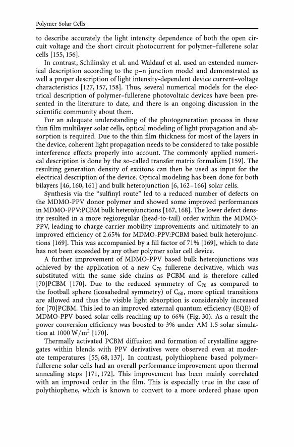
Chirvase et al. showed the effect of annealing on optical absorption to berather correlated with a molecular diffusion of PCBM out of the polythio-phene matrix [175]. Furthermore, the growth of PCBM clusters led to the for-mation of percolation paths and thus to improved photocurrents. Improvedordering of P3HT domains via interchain interaction [176] and a reduction ofinterface defects [177] has been previously connected to thermal annealing.Chirvase et al. showed that thermal annealing of pristine PCBM or P3HT filmsyielded only slight changes in the absorption, whereas annealing of blendsresulted in a large increase of P3HT absorption (see Fig. 32) [175].
The growth of large micron-sized PCBM crystal domains depended on theinitial concentration of PCBM in the blend as well as on the duration of the
H. Hoppe · N.S. Sariciftci
Fig. 32 Absorption spectra of a P3HT:PCBM composite film as cast (solid curve) andafter four successive thermal annealing steps, as indicated in the legend. The PCBM con-centration is 67%. (Reprinted with permission from [175], © 2004, Institute of PhysicsPublishing)
annealing process. Figure 33 shows the surface topography of P3HT:PCBMfilms without and with an aluminum electrode for two different PCBM con-centrations (50 and 75%). Clearly a dendrite structure is observed with in-creasing size for increasing PCBM content.
Kim et al. suggested that vertical phase segregation between P3HT andPCBM results from the thermal annealing [178], where P3HT is segregatedadjacent to the PEDOT:PSS electrode. Thus the holes could be transportedmore efficiently to the PEDOT:PSS electrode and electrons directly to the topaluminum contact, yielding better diode rectification [178]. In addition, theauthors investigated the influence of the annealing temperature on the deviceparameters and found the best results for annealing at 140 ◦C.
Yang et al. reported TEM and corresponding electron diffraction resultsof P3HT:PCBM blends [179]. An increase in crystallinity for both P3HT andPCBM phases as well as a fibrillar P3HT morphology with extended lengthare developed due to annealing [179]. The authors concluded that the expand-ing of the crystalline domains results in improved charge transport and deviceperformance. Figure 34 shows the TEM images together with the electrondiffraction images for the untreated and the annealed P3HT:PCBM blend.
Here the P3HT backbone is oriented vertically to the P3HT fibrils, with theπ–π stacking direction parallel to the fibril axis of the P3HT crystals [180].Hence, there are better charge carrier mobilities resulting along the π–π
stacking direction (long axis of fibrils).Erb et al. investigated the crystalline structure of P3HT:PCBM bulk hetero-
junctions by grazing incidence X-ray diffraction (GID-XRD) [181], showing

Polymer Solar Cells
Fig. 33 Tapping mode AFM images of P3HT:PCBM films without (a, b) and with alu-minum top electrode (c, d) at different PCBM concentrations. Large crystalline PCBMdendrites are observed for the larger fullerene concentration. (Reprinted with permissionfrom [175], © 2004, Institute of Physics Publishing)
Fig. 34 TEM images in combination with electron diffraction of a untreated and b therm-ally annealed P3HT:PCBM blend films. (Reprinted with permission from [179], © 2005,American Chemical Society)
that upon annealing P3HT crystallites with a dimension of about 10 nm aregrown. The polymer backbone orientation within these crystallites was foundto be parallel to the substrate, with the side chains oriented perpendicular

H. Hoppe · N.S. Sariciftci
to the substrate (a-axis orientation of P3HT crystallites). The XRD signalsbefore and after thermal annealing of P3HT:PCBM composites are shown inFig. 35.
Fig. 35 Diffraction diagram (grazing incidence) of untreated and annealed P3HT:PCBMblend films deposited on glass/ITO/PEDOT:PSS substrates (left). The corresponding a-axis orientation of the crystals is shown on the right. (Reproduced with permissionfrom [181], © 2005, Wiley-VCH)
The authors also correlated the increase in device efficiency with an in-creased crystallinity in the P3HT phase, but in contrast to Kim et al. theydid not detect any PCBM crystals in the blend film [181]. Interestingly, theobserved increase in optical absorption in the range of 1.9 to 3.0 eV upon an-nealing is directly correlated to the crystallization-induced ordering of P3HTin these blends (see with Fig. 36) [182].
It has been shown earlier by electron diffraction that PCBM is capable ofself-organizing into crystalline order in pristine PCBM films [184]. In a morecomprehensive study on MDMO-PPV:PCBM blends with varying composition,Yang et al. detected diffraction fringes in all films. The authors concluded thatPCBM evolves in nanosized crystallites in the blend. Furthermore, upon an-nealing, the PCBM will organize into larger crystals—thereby destroying theoriginal blend morphology. A conclusion of morphological instability at el-evated temperatures was drawn [68]. In contrast to these observations, Yanget al. found a remarkable morphological stability over 1000 h at elevated tem-peratures of 70 ◦C for accelerated aging under illumination for the P3HT:PCBMblends [179]. Hence, they suggested that the ability of P3HT to crystallize hasa stabilizing effect on the blend morphology. Schuller et al. reported similar re-sults for an even higher temperature of 85 ◦C under simultaneous illuminationwith half a sun intensity at short circuit conditions [185]. Drees et al. demon-strated that by introducing an epoxy group into PCBM, the fullerenes could belinked together and polymerized by application of a catalyst in combinationwith annealing [186]. Thus, in comparison with conventional P3HT:PCBM 1 : 2

Polymer Solar Cells
Fig. 36 XRD crystallinity (a) and absorption coefficient (b) of P3HT:PCBM blends spincast from either chlorobenzene (left) or chloroform (right) at various annealing tem-peratures. Interestingly, the increase in crystallinity is accompanied by a quantitativelycorrelated increase in optical absorption in the 2.0–2.5 eV region. (Reprinted from [183],© 2006, with permission from Elsevier)
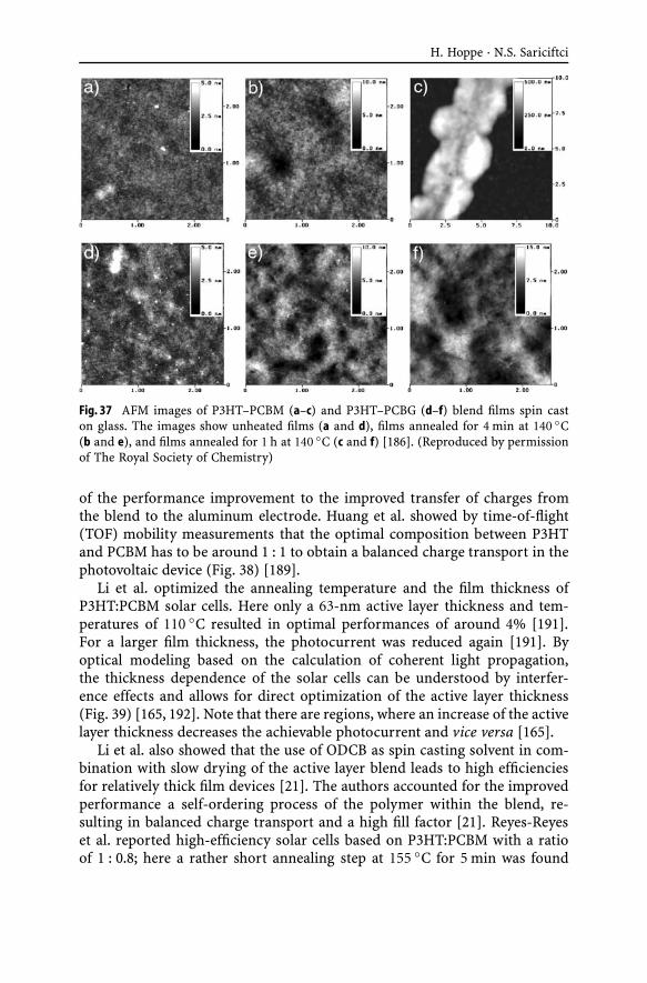
blends a morphological stabilization could be achieved. Figure 37 shows sometapping mode AFM images obtained on P3HT:PCBM and P3HT:PCBG blendfilms, both untreated and after thermal stress (annealing). Clearly the phaseseparation inside the PCBG containing blend is stopped before larger fullerenecrystallites (Fig. 37c) can be developed.
Also Sivully et al. stabilized the P3HT:PCBM thin film nanomorphology, butin this case via application of amphiphilic diblock copolymers [187]. Reducingthe PCBM concentration in blends with P3HT further down to less than 45%,Ma et al. confirmed that even at temperatures as high as 150 ◦C the film morph-ology was not considerably changed after 2 h and the overgrowth of fullereneaggregates was suppressed [18]. Thus, several encouraging results have beenobtained so far toward long-term stable polymer–fullerene solar cells.
Recently there have been several reports published on 4–5% record ef-ficiencies obtained on the P3HT:PCBM bulk heterojunction solar cell [18–21, 165, 188–190]. Ma et al. showed that annealing temperatures of 150 ◦C arerequired to obtain the highest efficiencies [18]. The authors assigned part
H. Hoppe · N.S. Sariciftci
Fig. 37 AFM images of P3HT–PCBM (a–c) and P3HT–PCBG (d–f) blend films spin caston glass. The images show unheated films (a and d), films annealed for 4 min at 140 ◦C(b and e), and films annealed for 1 h at 140 ◦C (c and f) [186]. (Reproduced by permissionof The Royal Society of Chemistry)
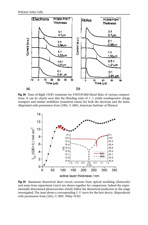
of the performance improvement to the improved transfer of charges fromthe blend to the aluminum electrode. Huang et al. showed by time-of-flight(TOF) mobility measurements that the optimal composition between P3HTand PCBM has to be around 1 : 1 to obtain a balanced charge transport in thephotovoltaic device (Fig. 38) [189].
Li et al. optimized the annealing temperature and the film thickness ofP3HT:PCBM solar cells. Here only a 63-nm active layer thickness and tem-peratures of 110 ◦C resulted in optimal performances of around 4% [191].For a larger film thickness, the photocurrent was reduced again [191]. Byoptical modeling based on the calculation of coherent light propagation,the thickness dependence of the solar cells can be understood by interfer-ence effects and allows for direct optimization of the active layer thickness(Fig. 39) [165, 192]. Note that there are regions, where an increase of the activelayer thickness decreases the achievable photocurrent and vice versa [165].
Li et al. also showed that the use of ODCB as spin casting solvent in com-bination with slow drying of the active layer blend leads to high efficienciesfor relatively thick film devices [21]. The authors accounted for the improvedperformance a self-ordering process of the polymer within the blend, re-sulting in balanced charge transport and a high fill factor [21]. Reyes-Reyeset al. reported high-efficiency solar cells based on P3HT:PCBM with a ratioof 1 : 0.8; here a rather short annealing step at 155 ◦C for 5 min was found
Polymer Solar Cells
Fig. 38 Time-of-flight (TOF) transients for P3HT:PCBM blend films of various composi-tions. It can be clearly seen that the blending ratio of 1 : 1 yields nondispersive chargetransport and similar mobilities (transition times) for both the electrons and the holes.(Reprinted with permission from [189], © 2005, American Institute of Physics)
Fig. 39 Maximum theoretical short circuit currents from optical modeling (diamonds)and some from experiment (stars) are shown together for comparison. Indeed the exper-imentally determined photocurrents closely follow the theoretical prediction in the rangeinvestigated. The inset shows a corresponding I–V curve for the best device. (Reproducedwith permission from [165], © 2007, Wiley-VCH)
H. Hoppe · N.S. Sariciftci
to lead to the highest performances [19]. The authors attributed part ofthe success to a changed morphology as shown by AFM measurements. Ina correlated study, the authors improved the annealing conditions for thickeractive layers, thereby reducing the fullerene content even further down toabout 38% [20]. Using high-resolution TEM, they detected small PCBM crys-tallites having sizes between 10 and 20 nm. The authors concluded that theindividual crystallization of both materials requires a fine adjustment of thethermal treatment for optimal results [20].
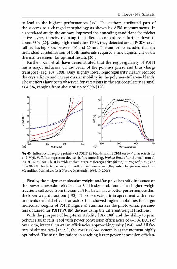
Further, Kim et al. have demonstrated that the regioregularity of P3HThas a major influence on the order of the polymer phase and thus chargetransport (Fig. 40) [190]. Only slightly lower regioregularity clearly reducedthe crystallinity and charge carrier mobility in the polymer–fullerene blends.These effects have been observed for variations in the regioregularity as smallas 4.5%, ranging from about 90 up to 95% [190].
Fig. 40 Influence of regioregularity of P3HT in blends with PCBM on I–V characteristicsand EQE. Full lines represent devices before annealing, broken lines after thermal anneal-ing at 140 ◦C for 2 h. It is evident that larger regioregularity (black, 95.2%; red, 93%; andblue 90.7%) leads to larger photovoltaic performances. (Reprinted by permission fromMacmillan Publishers Ltd: Nature Materials [190], © 2006)
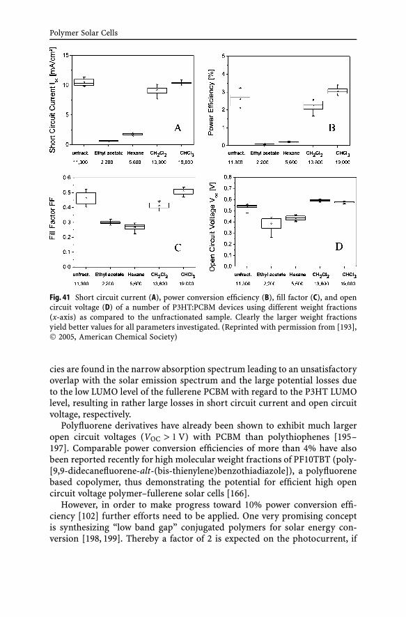
Finally, the polymer molecular weight and/or polydispersity influence onthe power conversion efficiencies: Schilinsky et al. found that higher weightfractions collected from the same P3HT batch show better performances thanthe lower weight fractions [193]. This observation is in agreement with meas-urements on field-effect transistors that showed higher mobilities for largermolecular weights of P3HT. Figure 41 summarizes the photovoltaic parame-ters obtained for P3HT:PCBM devices using the different weight fractions.
With the prospect of long-term stability [185, 188] and the ability to printpolymer solar cells [188] with power conversion efficiencies of 4–5%, EQEs ofover 75%, internal quantum efficiencies approaching unity [194], and fill fac-tors of almost 70% [18, 21], the P3HT:PCBM system is at the moment highlyoptimized. The main limitations in reaching larger power conversion efficien-
Polymer Solar Cells
Fig. 41 Short circuit current (A), power conversion efficiency (B), fill factor (C), and opencircuit voltage (D) of a number of P3HT:PCBM devices using different weight fractions(x-axis) as compared to the unfractionated sample. Clearly the larger weight fractionsyield better values for all parameters investigated. (Reprinted with permission from [193],© 2005, American Chemical Society)
cies are found in the narrow absorption spectrum leading to an unsatisfactoryoverlap with the solar emission spectrum and the large potential losses dueto the low LUMO level of the fullerene PCBM with regard to the P3HT LUMOlevel, resulting in rather large losses in short circuit current and open circuitvoltage, respectively.
Polyfluorene derivatives have already been shown to exhibit much largeropen circuit voltages (VOC > 1 V) with PCBM than polythiophenes [195–197]. Comparable power conversion efficiencies of more than 4% have alsobeen reported recently for high molecular weight fractions of PF10TBT (poly-[9,9-didecanefluorene-alt-(bis-thienylene)benzothiadiazole]), a polyfluorenebased copolymer, thus demonstrating the potential for efficient high opencircuit voltage polymer–fullerene solar cells [166].
However, in order to make progress toward 10% power conversion effi-ciency [102] further efforts need to be applied. One very promising conceptis synthesizing “low band gap” conjugated polymers for solar energy con-version [198, 199]. Thereby a factor of 2 is expected on the photocurrent, if

H. Hoppe · N.S. Sariciftci
charge transport properties remain the same. Energetically it appears mostlyfavorable to lower the LUMO level of the polymer and thus reduce the bandgap to allow for photon harvesting in the long wavelength range, while main-taining the open circuit voltage due a similar deep HOMO level. This imagecorresponds to the “ideal donor polymer” electronic properties [200].
One of the first employed low band gap materials in polymer–fullerene so-lar cells was PTPTB [201–203], extending the absorption spectrum to about750 nm and yielding 1% power conversion efficiency [203]. Colladet et al. ex-tended the absorption spectrum down to 800 nm based on thienylene–PPVderivatives [204]. Using a polyfluorene based copolymer, Zhou et al. achievedpower conversion efficiencies of about 2.2%, with a spectral absorption rangecomparable to that of P3HT [205]. Campos et al. achieved sensitization ofsolar energy conversion down to 900 nm [206]. So far the largest range ofabsorption up to 1000 nm deep in the infrared region was demonstrated
Fig. 42 Chemical structure (a) and absorption spectrum (b) of APFO-Green1, PCBM,and BTPF. The EQE (c) and I–V characteristics (d) under 100 mW/cm2 solar spectrumsimulation of APFO-Green1:PCBM 1 : 4 (filled circles) and APFO-Green1:BTPF 1 : 4 (opencircles) photovoltaic devices are also shown. (Reprinted with permission from [207],© 2004, American Institute of Physics)
Polymer Solar Cells
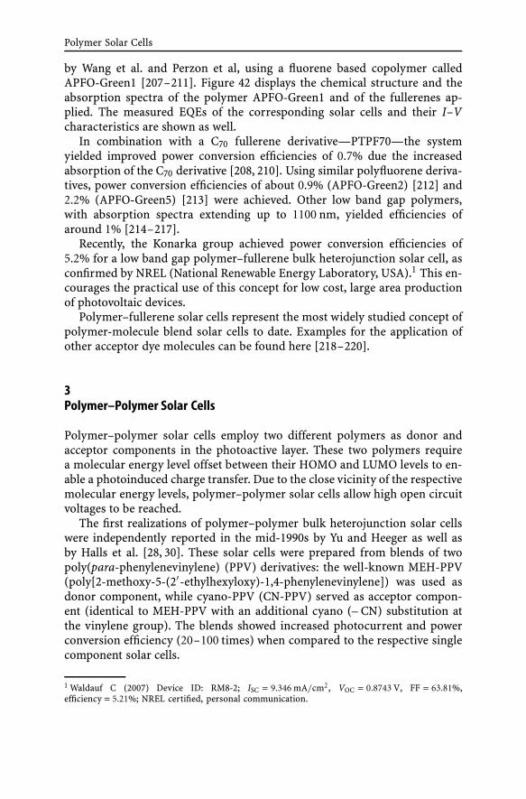
by Wang et al. and Perzon et al, using a fluorene based copolymer calledAPFO-Green1 [207–211]. Figure 42 displays the chemical structure and theabsorption spectra of the polymer APFO-Green1 and of the fullerenes ap-plied. The measured EQEs of the corresponding solar cells and their I–Vcharacteristics are shown as well.
In combination with a C70 fullerene derivative—PTPF70—the systemyielded improved power conversion efficiencies of 0.7% due the increasedabsorption of the C70 derivative [208, 210]. Using similar polyfluorene deriva-tives, power conversion efficiencies of about 0.9% (APFO-Green2) [212] and2.2% (APFO-Green5) [213] were achieved. Other low band gap polymers,with absorption spectra extending up to 1100 nm, yielded efficiencies ofaround 1% [214–217].
Recently, the Konarka group achieved power conversion efficiencies of5.2% for a low band gap polymer–fullerene bulk heterojunction solar cell, asconfirmed by NREL (National Renewable Energy Laboratory, USA).1 This en-courages the practical use of this concept for low cost, large area productionof photovoltaic devices.
Polymer–fullerene solar cells represent the most widely studied concept ofpolymer-molecule blend solar cells to date. Examples for the application ofother acceptor dye molecules can be found here [218–220].
3Polymer–Polymer Solar Cells
Polymer–polymer solar cells employ two different polymers as donor andacceptor components in the photoactive layer. These two polymers requirea molecular energy level offset between their HOMO and LUMO levels to en-able a photoinduced charge transfer. Due to the close vicinity of the respectivemolecular energy levels, polymer–polymer solar cells allow high open circuitvoltages to be reached.
The first realizations of polymer–polymer bulk heterojunction solar cellswere independently reported in the mid-1990s by Yu and Heeger as well asby Halls et al. [28, 30]. These solar cells were prepared from blends of twopoly(para-phenylenevinylene) (PPV) derivatives: the well-known MEH-PPV(poly[2-methoxy-5-(2′-ethylhexyloxy)-1,4-phenylenevinylene]) was used asdonor component, while cyano-PPV (CN-PPV) served as acceptor compon-ent (identical to MEH-PPV with an additional cyano (– CN) substitution atthe vinylene group). The blends showed increased photocurrent and powerconversion efficiency (20–100 times) when compared to the respective singlecomponent solar cells.
1 Waldauf C (2007) Device ID: RM8-2; ISC = 9.346 mA/cm2, VOC = 0.8743 V, FF = 63.81%,efficiency = 5.21%; NREL certified, personal communication.
H. Hoppe · N.S. Sariciftci
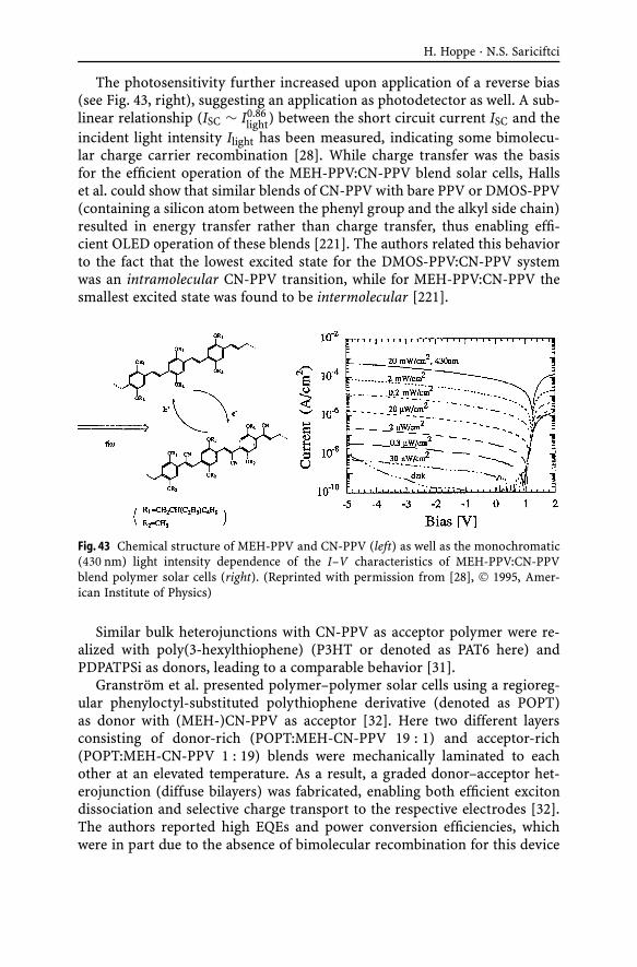
The photosensitivity further increased upon application of a reverse bias(see Fig. 43, right), suggesting an application as photodetector as well. A sub-linear relationship (ISC ∼ I0.86
light) between the short circuit current ISC and theincident light intensity Ilight has been measured, indicating some bimolecu-lar charge carrier recombination [28]. While charge transfer was the basisfor the efficient operation of the MEH-PPV:CN-PPV blend solar cells, Hallset al. could show that similar blends of CN-PPV with bare PPV or DMOS-PPV(containing a silicon atom between the phenyl group and the alkyl side chain)resulted in energy transfer rather than charge transfer, thus enabling effi-cient OLED operation of these blends [221]. The authors related this behaviorto the fact that the lowest excited state for the DMOS-PPV:CN-PPV systemwas an intramolecular CN-PPV transition, while for MEH-PPV:CN-PPV thesmallest excited state was found to be intermolecular [221].
Fig. 43 Chemical structure of MEH-PPV and CN-PPV (left) as well as the monochromatic(430 nm) light intensity dependence of the I–V characteristics of MEH-PPV:CN-PPVblend polymer solar cells (right). (Reprinted with permission from [28], © 1995, Amer-ican Institute of Physics)
Similar bulk heterojunctions with CN-PPV as acceptor polymer were re-alized with poly(3-hexylthiophene) (P3HT or denoted as PAT6 here) andPDPATPSi as donors, leading to a comparable behavior [31].
Granström et al. presented polymer–polymer solar cells using a regioreg-ular phenyloctyl-substituted polythiophene derivative (denoted as POPT)as donor with (MEH-)CN-PPV as acceptor [32]. Here two different layersconsisting of donor-rich (POPT:MEH-CN-PPV 19 : 1) and acceptor-rich(POPT:MEH-CN-PPV 1 : 19) blends were mechanically laminated to eachother at an elevated temperature. As a result, a graded donor–acceptor het-erojunction (diffuse bilayers) was fabricated, enabling both efficient excitondissociation and selective charge transport to the respective electrodes [32].The authors reported high EQEs and power conversion efficiencies, whichwere in part due to the absence of bimolecular recombination for this device
Polymer Solar Cells
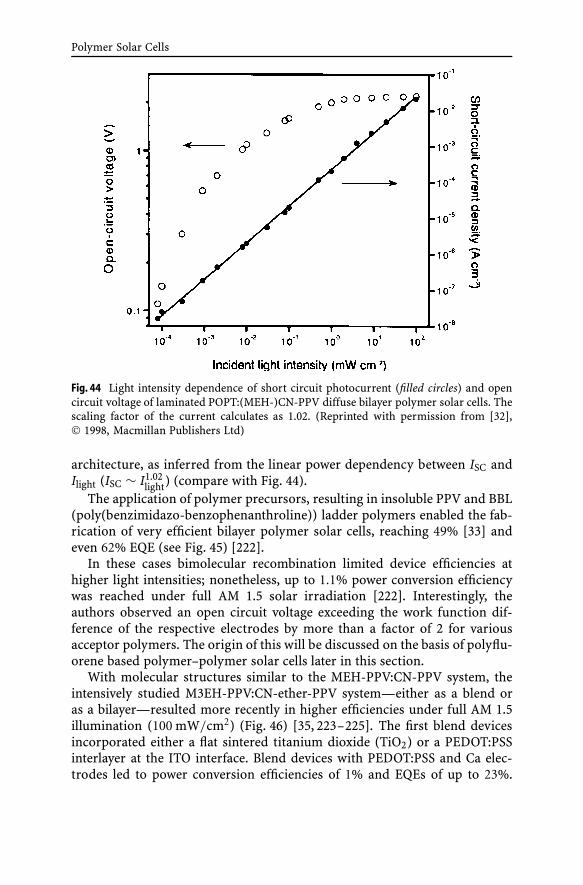
Fig. 44 Light intensity dependence of short circuit photocurrent (filled circles) and opencircuit voltage of laminated POPT:(MEH-)CN-PPV diffuse bilayer polymer solar cells. Thescaling factor of the current calculates as 1.02. (Reprinted with permission from [32],© 1998, Macmillan Publishers Ltd)
architecture, as inferred from the linear power dependency between ISC andIlight (ISC ∼ I1.02
light) (compare with Fig. 44).The application of polymer precursors, resulting in insoluble PPV and BBL
(poly(benzimidazo-benzophenanthroline)) ladder polymers enabled the fab-rication of very efficient bilayer polymer solar cells, reaching 49% [33] andeven 62% EQE (see Fig. 45) [222].
In these cases bimolecular recombination limited device efficiencies athigher light intensities; nonetheless, up to 1.1% power conversion efficiencywas reached under full AM 1.5 solar irradiation [222]. Interestingly, theauthors observed an open circuit voltage exceeding the work function dif-ference of the respective electrodes by more than a factor of 2 for variousacceptor polymers. The origin of this will be discussed on the basis of polyflu-orene based polymer–polymer solar cells later in this section.
With molecular structures similar to the MEH-PPV:CN-PPV system, theintensively studied M3EH-PPV:CN-ether-PPV system—either as a blend oras a bilayer—resulted more recently in higher efficiencies under full AM 1.5illumination (100 mW/cm2) (Fig. 46) [35, 223–225]. The first blend devicesincorporated either a flat sintered titanium dioxide (TiO2) or a PEDOT:PSSinterlayer at the ITO interface. Blend devices with PEDOT:PSS and Ca elec-trodes led to power conversion efficiencies of 1% and EQEs of up to 23%.

H. Hoppe · N.S. Sariciftci
Fig. 45 Chemical structures (a), energy levels (b), and device structure (c) of PPV/BBL bi-layers. High EQE (or IPCE) is shown together with the absorption spectrum of PPV/BBLbilayer solar cells. (Left: Reprinted with permission from [28], © 2000, American Insti-tute of Physics; Right: Reprinted with permission from [193], © 2004, American ChemicalSociety)
Fig. 46 Characteristics of solar cells based on M3EH-PPV:CN-ether-PPV blends (1 : 1ratio by mass) for different thicknesses of the active layer after annealing at 110 ◦C.a Comparison of the IPCE and the absorption spectra of CN-ether-PPV (squares) andM3EH-PPV (triangles) of the blend layer (black line). b I–V characteristics under whitelight illumination at intensity of 100 mW/cm2. (Reprinted with permission from [35],© 2005, American Chemical Society)
Breeze et al. found that the short circuit current increased as the blend layerthickness decreased, indicating the devices to be limited by charge transportlosses [223]. Further improvements were achieved by Kietzke et al. using ther-mal annealing of blend layers reaching EQEs of 31% and power conversionefficiencies of 1.7%, which to date is one of the best efficiencies observed for
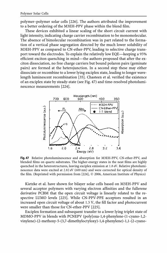
Polymer Solar Cells
polymer–polymer solar cells [226]. The authors attributed the improvementto a better ordering of the M3EH-PPV phase within the blend film.
These devices exhibited a linear scaling of the short circuit current withlight intensity, indicating charge carrier recombination to be monomolecular.The absence of bimolecular recombination was in part related to the forma-tion of a vertical phase segregation directed by the much lower solubility ofM3EH-PPV as compared to CN-ether-PPV, leading to selective charge trans-port toward the electrodes. To explain the relatively low EQE—keeping a 95%efficient exciton quenching in mind—the authors proposed that after the ex-citon dissociation, no free charge carriers but bound polaron pairs (geminatepairs) are formed at the heterojunction. In a second step these may eitherdissociate or recombine to a lower lying exciplex state, leading to longer wave-length luminescent recombination [35]. Chasteen et al. verified the existenceof an exciplex state by steady-state (see Fig. 47) and time-resolved photolumi-nescence measurements [224].
Fig. 47 Relative photoluminescence and absorption for M3EH-PPV, CN-ether-PPV, andblended films on quartz substrates. The higher-energy states in the neat films are highlyquenched in the heterostructures, leaving exciplex emission at 1.8 eV. Relative photolumi-nescence data were excited at 2.82 eV (600 nm) and were corrected for optical density ofthe film. (Reprinted with permission from [224], © 2006, American Institute of Physics)
Kietzke et al. have shown for bilayer solar cells based on M3EH-PPV andseveral acceptor polymers with varying electron affinities and the fullerenederivative PCBM that the open circuit voltage is linearly related to the re-spective LUMO levels [225]. While CN-PPV-PPE acceptors resulted in anincreased open circuit voltage of about 1.5 V, the fill factor and photocurrentwere smaller than those for CN-ether-PPV [225].
Exciplex formation and subsequent transfer to a lower lying triplet state ofMDMO-PPV in blends with PCNEPV (poly[oxa-1,4-phenylene-(1-cyano-1,2-vinylene)-(2-methoxy-5-(3,7-dimethyloctyloxy)-1,4-phenylene)-1,1-(2-cyano-

H. Hoppe · N.S. Sariciftci
vinylene)-1,4-phenylene]) were identified as efficiency-limiting processes forphotovoltaic devices [227–230]. Veenstra et al. demonstrated power conver-sion efficiencies of 0.75% by thermal treatment of the MDMO-PPV:PCNEPVactive layer, by which the nanomorphology was altered [227]. For a set ofPCNEPVs with three different molecular weights, the annealing tempera-ture, under which the photocurrent was improved, showed strong correlationto the respective glass transition temperature of each weight fraction [227].Quist et al. showed that annealing led to the formation of PCNEPV-richdomains, enabling the photoinduced electrons to diffuse away from the het-erojunction interface and thus to escape from geminate recombination [228].The authors further pointed out that low charge carrier mobility in combi-nation with restricted charge collection at the electrodes were the limitingfactors for solar cell performance.
Offermans et al. used several spectroscopic methods to study the forma-tion and luminescence decay of exciplexes as a function of photoexcitation (ofeither polymer), and subsequent charge transfer at the heterojunction [229].Exciplex formation was followed by a relaxation to the lower lying triplet stateT1 of the MDMO-PPV. The energetic scheme is depicted in Fig. 48.
While internal electric fields may offer a route to charge separation outof the exciplex, the free charge carriers may then recombine more easily tothe triplet state due to the loss of spin correlation. This process resulted inelectric field enhanced triplet formation and was identified as the major lossmechanism for the photovoltaic performance of MDMO-PPV:PCNEPV bulkheterojunctions [229, 230]. Using a set of several electron-accepting polymers,among them PCNEPV, Veldman et al. demonstrated that the open circuit volt-age is again linearly related to the LUMO level of the acceptor. Since thecharge separated state is lower than the singlet excited state and higher thanthe triplet state, this opens up the route to triplet-mediated recombination atthe interface with MDMO-PPV [230].
Whereas few material systems studied yielding up to 1.5% power con-version efficiency are unique [231–234], blends and bilayers of polyflu-orene based copolymers were most often investigated. PFB (poly[9,9′-dioctylfluorene-co-bis-N,N′-(4-butylphenyl)-bis-N,N′-phenyl-1,4-phenylene-diamine]) is commonly used as the donor and F8BT (poly(9,9′-dioctylfluor-ene-co-benzothiadiazole)) as the electron acceptor. While F8BT—due toits highly luminescent character—is used in OLEDs as well, PFB is re-placed by a similar donor named TFB (poly[9,9′-dioctylfluorene-co-N-(4-butylphenyl)diphenylamine]) for improved luminescence efficiency—a factthat we will shed light on later in this section.
In a first study on F8BT:PFB blends, Halls et al. studied morphological ef-fects that arise from a complicated interplay between solidification by solventevaporation, phase separation, and (de)wetting [235]. The authors showedthat lateral phase separation can simultaneously exist on both the microme-ter and nanometer scales, depending on the rate of solvent evaporation. They
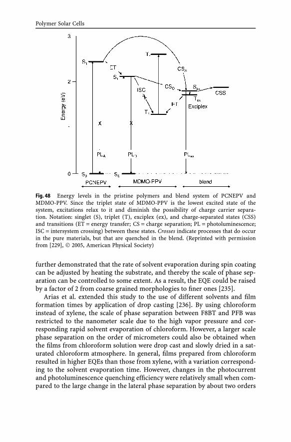
Polymer Solar Cells
Fig. 48 Energy levels in the pristine polymers and blend system of PCNEPV andMDMO-PPV. Since the triplet state of MDMO-PPV is the lowest excited state of thesystem, excitations relax to it and diminish the possibility of charge carrier separa-tion. Notation: singlet (S), triplet (T), exciplex (ex), and charge-separated states (CSS)and transitions (ET = energy transfer; CS = charge separation; PL = photoluminescence;ISC = intersystem crossing) between these states. Crosses indicate processes that do occurin the pure materials, but that are quenched in the blend. (Reprinted with permissionfrom [229], © 2005, American Physical Society)
further demonstrated that the rate of solvent evaporation during spin coatingcan be adjusted by heating the substrate, and thereby the scale of phase sep-aration can be controlled to some extent. As a result, the EQE could be raisedby a factor of 2 from coarse grained morphologies to finer ones [235].
Arias et al. extended this study to the use of different solvents and filmformation times by application of drop casting [236]. By using chloroforminstead of xylene, the scale of phase separation between F8BT and PFB wasrestricted to the nanometer scale due to the high vapor pressure and cor-responding rapid solvent evaporation of chloroform. However, a larger scalephase separation on the order of micrometers could also be obtained whenthe films from chloroform solution were drop cast and slowly dried in a sat-urated chloroform atmosphere. In general, films prepared from chloroformresulted in higher EQEs than those from xylene, with a variation correspond-ing to the solvent evaporation time. However, changes in the photocurrentand photoluminescence quenching efficiency were relatively small when com-pared to the large change in the lateral phase separation by about two orders

H. Hoppe · N.S. Sariciftci
of magnitude. Multiple scale phase separation was responsible for this: thelarger, micron-sized phase domains were themselves not purely one mate-rial but exhibited some internal nanometer-sized phase separation as well(see Fig. 49). The multiple scale phase separation arose from several stagesin film formation and phase separation, including heterogeneous nucleation,spinoidal decomposition, hydrodynamic regimes, coalescence, and some pos-sible dewetting or liquid film instability effects. Finally, by combination offluorescence microscopy, fluorescence SNOM, and tapping mode AFM theauthors proved the luminescent F8BT to be the phase elevated at the surfaceof the film evolving in the large-scale phase separated blend films [236].
Snaith et al. investigated F8BT:PFB blends with respect to the blendingratio [237]. They found that the photoluminescence quenching efficiencywas rather insensitive to the blending ratio, whereas the highest EQEs were
Fig. 49 AFM images of PFB:F8BT film spin-coated from xylene solution clearly demon-strating phase separation to exist on two scales. Left: height images; right: phase responseimages. a 10 µm × 10 µm and b 500 nm × 500 nm, which was taken in the vicinity ofthe sample marked by the white square in (a). (Reprinted with permission from [236],© 2004, American Chemical Society)

Polymer Solar Cells
obtained for F8BT-enriched blends (PFB:F8BT 1 : 5). They attributed thisdiscrepancy between the photoluminescence quenching and EQE to chargetransport limitation rather than to charge generation. The authors also de-veloped a simple model describing the interfacial area between F8BT- andPFB-rich domains and found a linear trend with respect to the EQE [237].
A further refinement of the scale of phase separation was recently demon-strated by Xia and Friend using inkjet printing (IJP) and thereby doubling theEQE [238]. As demonstrated by fluorescence and atomic force microscopies,this originates from a more rapid drying process of inkjet printed films ascompared to spin cast ones (see Fig. 50). The small volume and hence thelarge surface to volume ratio of each IJP droplet led to this fast evaporationand drying.
Fig. 50 Fluorescent microscopic pictures of TFB:F8BT blend films produced by spin-coating (a), inkjet printing at room temperature (RT) (b), and inkjet printing at 40 ◦C (c).The insets show the corresponding AFM pictures (10 µm × 10 µm). Blend films weredeposited onto ITO-coated substrates. A reduction in scale of phase separation froma through c is demonstrated. (Reprinted with permission from [238], © 2005, AmericanChemical Society)
Kietzke et al. suggested another approach to control the scale of phase sep-aration by preparation of dispersions of solid polymer nanoparticles [239,240]. To achieve the polymer nanoparticles, either a pristine polymer ora polymer blend solution are placed into a water/surfactant mixture. Uponultrasonication and stirring, a miniemulsion is formed that directly leads tosolid polymer particles in aqueous solution by subsequent evaporation of thesolvent. The route of preparation is schematically shown in Fig. 51. Indeed,the EQE spectrum of spin cast solar cells was independent of the solvent usedin the miniemulsion process for blended nanoparticles [239]. Both concepts,dispersions of blends of pristine polymer particles (single PFB and singleF8BT particles, separately made) as well as dispersions of blended polymerparticles (PFB:F8BT blend particles), yielded comparable efficiencies to solu-tion processed blends, with the latter yielding a threefold larger EQE [240].
In another study Arias et al. showed that a vertical phase segregation couldbe induced in thin films spin cast from F8BT:PFB blends by interfacial modi-fication of the PEDOT:PSS layer with SAMs [241]. To introduce the SAM, thePEDOT:PSS layer was first modified by oxygen plasma treatment leading to
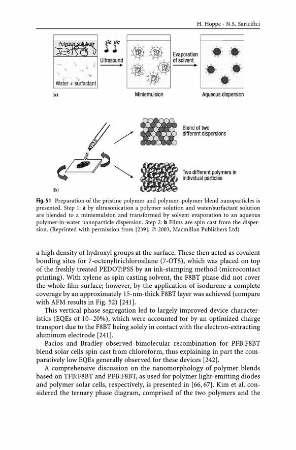
H. Hoppe · N.S. Sariciftci
Fig. 51 Preparation of the pristine polymer and polymer–polymer blend nanoparticles ispresented. Step 1: a by ultrasonication a polymer solution and water/surfactant solutionare blended to a miniemulsion and transformed by solvent evaporation to an aqueouspolymer-in-water nanoparticle dispersion. Step 2: b Films are spin cast from the disper-sion. (Reprinted with permission from [239], © 2003, Macmillan Publishers Ltd)
a high density of hydroxyl groups at the surface. These then acted as covalentbonding sites for 7-octenyltrichlorosilane (7-OTS), which was placed on topof the freshly treated PEDOT:PSS by an ink-stamping method (microcontactprinting). With xylene as spin casting solvent, the F8BT phase did not coverthe whole film surface; however, by the application of isodurene a completecoverage by an approximately 15-nm-thick F8BT layer was achieved (comparewith AFM results in Fig. 52) [241].
This vertical phase segregation led to largely improved device character-istics (EQEs of 10–20%), which were accounted for by an optimized chargetransport due to the F8BT being solely in contact with the electron-extractingaluminum electrode [241].
Pacios and Bradley observed bimolecular recombination for PFB:F8BTblend solar cells spin cast from chloroform, thus explaining in part the com-paratively low EQEs generally observed for these devices [242].
A comprehensive discussion on the nanomorphology of polymer blendsbased on TFB:F8BT and PFB:F8BT, as used for polymer light-emitting diodesand polymer solar cells, respectively, is presented in [66, 67]. Kim et al. con-sidered the ternary phase diagram, comprised of the two polymers and the

Polymer Solar Cells
Fig. 52 Topographical AFM images of PFB:F8BT deposited under different preparationconditions onto a monolayer printed on a PEDOT electrode: a spin-coating from xylenesolution; b spin-coating under a xylene-rich atmosphere from xylene solution; and c spin-coating from isodurene solution (leading to homogeneous F8BT coverage). d Short-circuitEQE action spectra of photovoltaic devices fabricated by spin-coating the blend solutionfrom xylene (filled circles), under a xylene-rich atmosphere (solid line), and from iso-durene (open circles). (Reprinted with permission from [241], © 2002, American Instituteof Physics)
solvent, for understanding the evolving blend morphology during the spin-coating process. A schematic for the three-dimensional phase composition ofthe TFB:F8BT blend film during and after film formation is presented [67].Essentially the same morphology has been found for PFB:F8BT blends, whichwas validated with the help of scanning Kelvin probe microscopy [243].Thereby it was further evidenced that a PFB capping layer reduced effectivelythe performance of the device due to its blocking of photogenerated elec-trons in the F8BT-rich phase from reaching the electrode. The same effect wasobserved earlier in polymer–fullerene blends as well [60, 244]. Chiesa et al.further elucidated that a simple bilayer structure is advantageous for effi-cient electron conduction and thus device operation [243], in accordance withArias et al. [241]. In addition Chiesa et al. detected the surface potential on ei-ther phase of the blend film to be logarithmically dependent on the impinginglight intensity [243].
A logarithmic relationship between light intensity and open circuit volt-age had been shown for bilayer polymer solar cells by Ramsdale et al. [125].This and the observation of an “overpotential” of the open circuit voltage withrespect to the work function difference of the two electrodes—as inferred

H. Hoppe · N.S. Sariciftci
from the MIM model [63, 245]—was explained by a charge concentrationdriven diffusion current in these bilayer devices (compare with Fig. 18) [125].The observed overpotential of 1 V was practically independent of cathodework function variations through 0.8 eV. Thus, at open circuit voltage, as de-fined by a net zero current through the device, the field driven drift current(injection) and concentration driven diffusion current simply cancel eachother. In a refined numerical model the same behavior can be closely simu-lated [129]. Furthermore, the authors showed that charge separation at thepolymer–polymer heterojunction leads to the formation of bound polaronpairs, which may either recombine monomolecularly or be dissociated intofree charges [129].
Snaith et al. related differences in open circuit voltage between bilayer andblend devices to parasitic shunt losses in the blends, when especially the PFBphase paths connect both the electrodes (see Fig. 53) [246].
Fig. 53 Dependence of open circuit voltage VOC on the architecture of PFB:F8BT solarcells. When the PFB phase can form percolation paths between both electrodes, the VOCis reduced considerably. (Reproduced with permission from [246], © 2004, Wiley-VCH)
Morteani et al. demonstrated that after photoexcitation and subsequentdissociation of an exciton at the polymer–polymer heterojunction, an inter-mediate bound geminate polaron pair is formed across the interface [56, 57].These geminate pairs may either dissociate into free charge carriers or col-lapse into an exciplex state, and either contribute to red-shifted photolumi-nescence or may be endothermically back-transferred to form a bulk excitonagain [57]. In photovoltaic operation the first route is desired, whereas thesecond route is an unwanted loss channel. Figure 54 displays the potentialenergy curves for the different states.
The authors showed by applying the Onsager model to electric field-dependent photoluminescence quenching data [49, 247, 248] that the gemi-
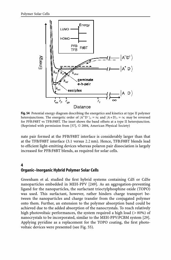
Polymer Solar Cells
Fig. 54 Potential energy diagram describing the energetics and kinetics at type II polymerheterojunctions. The energetic order of |A+D–〉r = ∞ and |A ∗ D〉r = ∞ may be reversedfor PFB:F8BT vs TFB:F8BT. The inset shows the band offsets at a type II heterojunction.(Reprinted with permission from [57], © 2004, American Physical Society)
nate pair formed at the PFB/F8BT interface is considerably larger than thatat the TFB/F8BT interface (3.1 versus 2.2 nm). Hence, TFB:F8BT blends leadto efficient light-emitting devices whereas polaron pair dissociation is largelyincreased for PFB:F8BT blends, as required for solar cells.
4Organic–Inorganic Hybrid Polymer Solar Cells
Greenham et al. studied the first hybrid systems containing CdS or CdSenanoparticles embedded in MEH-PPV [249]. As an aggregation-preventingligand for the nanoparticles, the surfactant trioctylphosphine oxide (TOPO)was used. This surfactant, however, rather hinders charge transport be-tween the nanoparticles and charge transfer from the conjugated polymeronto them. Further, an extension to the polymer absorption band could beachieved due to the added absorption of the nanocrystals. To reach relativelyhigh photovoltaic performances, the system required a high load (> 80%) ofnanocrystals to be incorporated, similar to the MEH-PPV:PCBM system [29].Applying pyridine as a replacement for the TOPO coating, the first photo-voltaic devices were presented (see Fig. 55).

H. Hoppe · N.S. Sariciftci
Fig. 55 Current–voltage curve for a MEH-PPV based device containing 90 wt % CdSe inthe dark (circles) and under monochromatic illumination at 514 nm (solid line). The ac-tive area of the device was 7.3 mm2, and the illumination was from a laser spot which wascontained within the active area. The maximum power density of the illumination was ap-proximately 5 W/m2. (Reprinted with permission from [249], © 1996, American PhysicalSociety)
A major step in the development of hybrid polymer solar cells wasachieved by blending CdSe nanoparticles with regioregular P3HT. In 2002,Huynh et al. reported AM 1.5 power conversion efficiencies of 1.7% and EQEsreaching 54% with that system [250]. In this study the aspect ratio of the CdSenanocrystals was varied roughly between 1 and 10, and the authors reportedthe best photovoltaic efficiencies for nanorods having the most elongatedstructure (7 by 60 nm) (see Fig. 56). The authors concluded that the elon-gated nanorod-like nanocrystals provide a better charge transport throughband transport than shorter ones, where many hopping processes betweenthe nanoparticles limit charge transport.
In a related study, Huynh et al. demonstrated control of the P3HT:CdSenanorod blend morphology in thin films by applying a solvent mixture ofchloroform and pyridine [251]. A pyridine concentration of about 8% yieldedthe finest intermixing of P3HT and CdSe nanorods, which was reflected bysmooth film topographies. A thermal annealing step was applied at reducedpressure to remove excess pyridine from the blend, and consequently improvethe EQE. The highest EQE was achieved for elongated nanorods, yielding al-most 60% after thermal treatment.
Pientka et al. studied photoinduced charge transfer from CdSe andInP nanocrystals onto MDMO-PPV [252, 253]. The authors confirmed theuse of pyridine to be favorable for efficient charge transfer as comparedto more extended octylphosphine-containing organic ligands around thenanoparticles. These results were obtained by using photoluminescencequenching, photoinduced charge transfer, and light-induced spin resonancemeasurements.

Polymer Solar Cells
Fig. 56 ECE (A) of 7-, 30-, and 60-nm-long CdSe nanorods having a diameter of 7 nm.Current–voltage characteristics in the dark and 0.1 mW/cm2 (B) and at AM 1.5 so-lar spectrum (C) of P3HT:CdSe hybrid solar cells. Photocurrent spectra of 60-nm-longnanorods with a diameter of 3 and 7 nm are compared in (D). From [250]. (Reprinted withpermission from American Association for the Advancement of Science (AAAS), © 2002.http://www.sciencemag.org)
CdSe nanocrystal based solar cells were substantially improved by Sunet al.: a twofold increase in the EQE was achieved for MDMO-PPV basedblends by application of CdSe nanotetrapods instead of nanorods [254]. Thetetrapods, due to their shape, induced better directed electron transport nor-mal to the film plane, yielding overall power conversion efficiencies of 1.8%.The current–voltage characteristics of this device are displayed in Fig. 57.
A further performance increase was achieved by application of 1,2,4-trichlorobenzene instead of chloroform as spin casting solvent: typical deviceefficiencies of 2.1% are reported [255]. The authors related this improve-ment to a vertical segregation of the CdSe tetrapods in the film. By usingthe same solvent for CdSe nanorods in combination with regioregular P3HT,photovoltaic devices consistently yielded power conversion efficiencies of2.6% [36]. This has also been related to the formation of P3HT fibrils in thefilm, resulting in improved hole transport properties expressed by larger pho-tocurrents and fill factors in comparison to the cases where chloroform orthiophene was used as solvent.
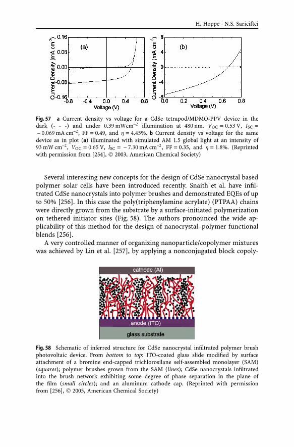
H. Hoppe · N.S. Sariciftci
Fig. 57 a Current density vs voltage for a CdSe tetrapod/MDMO-PPV device in thedark (- - -) and under 0.39 mWcm–2 illumination at 480 nm. VOC = 0.53 V, ISC =– 0.069 mA cm–2, FF = 0.49, and η = 4.45%. b Current density vs voltage for the same
device as in plot (a) illuminated with simulated AM 1.5 global light at an intensity of93 mW cm–2, VOC = 0.65 V, ISC = – 7.30 mA cm–2, FF = 0.35, and η = 1.8%. (Reprintedwith permission from [254], © 2003, American Chemical Society)
Several interesting new concepts for the design of CdSe nanocrystal basedpolymer solar cells have been introduced recently. Snaith et al. have infil-trated CdSe nanocrystals into polymer brushes and demonstrated EQEs of upto 50% [256]. In this case the poly(triphenylamine acrylate) (PTPAA) chainswere directly grown from the substrate by a surface-initiated polymerizationon tethered initiator sites (Fig. 58). The authors pronounced the wide ap-plicability of this method for the design of nanocrystal–polymer functionalblends [256].
A very controlled manner of organizing nanoparticle/copolymer mixtureswas achieved by Lin et al. [257], by applying a nonconjugated block copoly-
Fig. 58 Schematic of inferred structure for CdSe nanocrystal infiltrated polymer brushphotovoltaic device. From bottom to top: ITO-coated glass slide modified by surfaceattachment of a bromine end-capped trichlorosilane self-assembled monolayer (SAM)(squares); polymer brushes grown from the SAM (lines); CdSe nanocrystals infiltratedinto the brush network exhibiting some degree of phase separation in the plane ofthe film (small circles); and an aluminum cathode cap. (Reprinted with permissionfrom [256], © 2005, American Chemical Society)
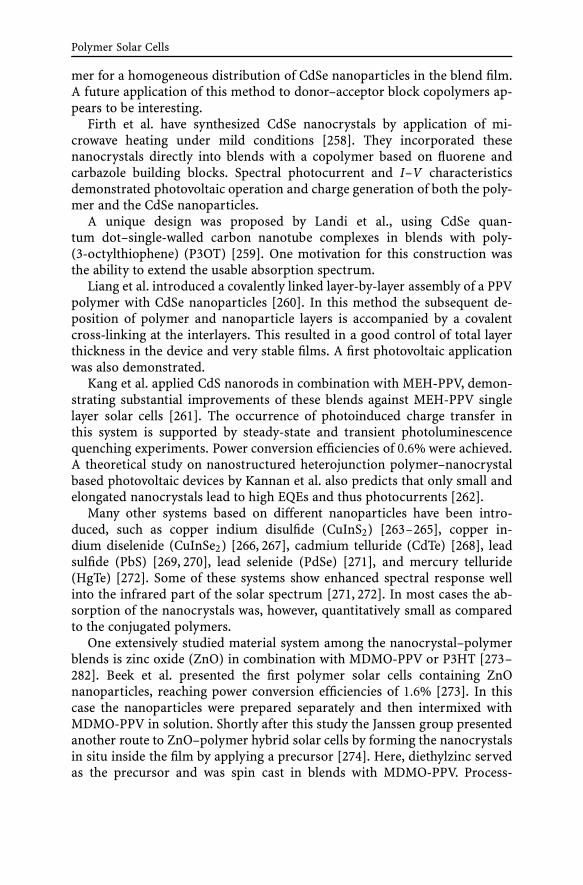
Polymer Solar Cells
mer for a homogeneous distribution of CdSe nanoparticles in the blend film.A future application of this method to donor–acceptor block copolymers ap-pears to be interesting.
Firth et al. have synthesized CdSe nanocrystals by application of mi-crowave heating under mild conditions [258]. They incorporated thesenanocrystals directly into blends with a copolymer based on fluorene andcarbazole building blocks. Spectral photocurrent and I–V characteristicsdemonstrated photovoltaic operation and charge generation of both the poly-mer and the CdSe nanoparticles.
A unique design was proposed by Landi et al., using CdSe quan-tum dot–single-walled carbon nanotube complexes in blends with poly-(3-octylthiophene) (P3OT) [259]. One motivation for this construction wasthe ability to extend the usable absorption spectrum.
Liang et al. introduced a covalently linked layer-by-layer assembly of a PPVpolymer with CdSe nanoparticles [260]. In this method the subsequent de-position of polymer and nanoparticle layers is accompanied by a covalentcross-linking at the interlayers. This resulted in a good control of total layerthickness in the device and very stable films. A first photovoltaic applicationwas also demonstrated.
Kang et al. applied CdS nanorods in combination with MEH-PPV, demon-strating substantial improvements of these blends against MEH-PPV singlelayer solar cells [261]. The occurrence of photoinduced charge transfer inthis system is supported by steady-state and transient photoluminescencequenching experiments. Power conversion efficiencies of 0.6% were achieved.A theoretical study on nanostructured heterojunction polymer–nanocrystalbased photovoltaic devices by Kannan et al. also predicts that only small andelongated nanocrystals lead to high EQEs and thus photocurrents [262].
Many other systems based on different nanoparticles have been intro-duced, such as copper indium disulfide (CuInS2) [263–265], copper in-dium diselenide (CuInSe2) [266, 267], cadmium telluride (CdTe) [268], leadsulfide (PbS) [269, 270], lead selenide (PdSe) [271], and mercury telluride(HgTe) [272]. Some of these systems show enhanced spectral response wellinto the infrared part of the solar spectrum [271, 272]. In most cases the ab-sorption of the nanocrystals was, however, quantitatively small as comparedto the conjugated polymers.
One extensively studied material system among the nanocrystal–polymerblends is zinc oxide (ZnO) in combination with MDMO-PPV or P3HT [273–282]. Beek et al. presented the first polymer solar cells containing ZnOnanoparticles, reaching power conversion efficiencies of 1.6% [273]. In thiscase the nanoparticles were prepared separately and then intermixed withMDMO-PPV in solution. Shortly after this study the Janssen group presentedanother route to ZnO–polymer hybrid solar cells by forming the nanocrystalsin situ inside the film by applying a precursor [274]. Here, diethylzinc servedas the precursor and was spin cast in blends with MDMO-PPV. Process-
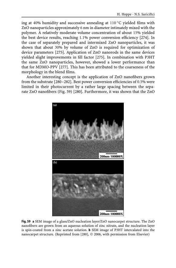
H. Hoppe · N.S. Sariciftci
ing at 40% humidity and successive annealing at 110 ◦C yielded films withZnO nanoparticles approximately 6 nm in diameter intimately mixed with thepolymer. A relatively moderate volume concentration of about 15% yieldedthe best device results, reaching 1.1% power conversion efficiency [274]. Inthe case of separately prepared and intermixed ZnO nanoparticles, it wasshown that about 30% by volume of ZnO is required for optimization ofdevice parameters [275]. Application of ZnO nanorods in the same devicesyielded slight improvements in fill factor [275]. In combination with P3HTthe same ZnO nanoparticles, however, showed a lower performance thanthat for MDMO-PPV [277]. This has been attributed to the coarseness of themorphology in the blend films.
Another interesting concept is the application of ZnO nanofibers grownfrom the substrate [280–282]. Best power conversion efficiencies of 0.5% werelimited in their photocurrent by a rather large spacing between the sepa-rate ZnO nanofibers (Fig. 59) [280]. Furthermore, it was shown that the ZnO
Fig. 59 a SEM image of a glass/ZnO nucleation layer/ZnO nanocarpet structure. The ZnOnanofibers are grown from an aqueous solution of zinc nitrate, and the nucleation layeris spin-coated from a zinc acetate solution. b SEM image of P3HT intercalated into thenanocarpet structure. (Reprinted from [280], © 2006, with permission from Elsevier)

Polymer Solar Cells
nanofiber growth can be controlled by a seed layer, and the application of anamphiphilic molecule as interface layer can help to reduce charge recombina-tion [281, 282].
Closely related to liquid electrolyte dye-sensitized solar cells (DSSCs,also known as “Grätzel cells”) [283, 284], the class of solid-state DSSCs hasbeen developed to improve device stability and reduce complications inthe production process [285–288]. Thus, although polymers can be utilizedas replacements for sensitizing dyes (as in liquid electrolyte DSSCs) [289–291], the main effort in applying conjugated polymers focuses on solid-stateDSSCs [45, 292–298]. With environmentally friendly production of this poly-mer based solid-state DSSC in mind, a device based on water-soluble poly-thiophene derivative has been presented as well [299].
Rather sophisticated structures of the TiO2 porous film were introducedby Coakley et al. [69, 70]. Based on a titanium(IV) tetraethoxide (TEOT)titania precursor in combination with a pluronic poly(ethylene oxide)–poly(propylene oxide)–poly(ethylene oxide) triblock copolymer (P123) as thestructure-directing agent, regular hexagonal structures (honeycomb) withpore sizes around 10 nm were prepared (Fig. 60).
Fig. 60 High-resolution SEM top view image of a mesoporous TiO2 film following calci-nation at 400 ◦C. The pore diameter in the plane of the film is ∼10 nm. (Reprinted withpermission from [70], © 2003, American Institute of Physics)
After production of the mesoporous TiO2 film, regioregular P3HT was in-filtrated into these pores followed by an annealing step. Even for the highestannealing temperatures of 200 ◦C the authors estimated a total polymer infil-tration of only 33%, since in the small pores the polymer has to form rathercoiled structures as indicated by a blue-shift in the polymer absorption andemission spectra. This coiling was proposed to be a reason for lower excitonand charge transport efficiencies, leading to estimated power conversion ef-ficiencies somewhat below 0.5% [70]. For larger pore diameters up to 80 nmobtained in anodic alumina, Coakley et al. observed an increase of the P3HThole mobility due to alignment of the polymer chains along the pores [300].

H. Hoppe · N.S. Sariciftci
Bartholomew and Heeger reported recently on the infiltration of P3HTin random nanocrystalline TiO2 networks [301]. The TiO2 networks wereproduced by spin-coating TiO2 nanocrystals modified by organics from dis-persion. Due to a low resulting porosity of the TiO2 film (Fig. 61), infiltrationof the polymer appeared to be difficult. Yet, the amount of infiltrated P3HTcould be effectively increased by using a lower molecular weight fraction ofthe polymer, in combination with annealing and surface modification of theTiO2 nanocrystals by applying amphiphilic Ru-based dyes [301].
Fig. 61 SEM image of a random nanocrystalline TiO2 film created by spin-coating. a Topview and b angled view of a cross section. The scale bars represent 500 nm. (Reproducedwith permission from [301], © 2005, Wiley-VCH)
Solid-state DSSCs have much lower efficiencies as compared to liquid elec-trolyte Grätzel cells, most probably due to charge transport and recombina-tion limitations. Ravirajan et al. reported that an additional PEDOT:PSS layerunder the hole-extracting gold electrode improved charge extraction, leadingto overall power conversion efficiencies of about 0.6% [302]. Further increasein the power conversion efficiency (0.7%) was reached for similarly con-structed devices, where the porous TiO2 layer was optimized in its intercon-necting network structure by applying structure-directing polystyrene-block-polyethylene oxide diblock copolymer templates (P(S-b-EO); Fig. 62) [303].
A straightforward approach to forming a conjugated polymer/nano-crystalline TiO2 hybrid bulk heterojunction was reported by van Halet al. [304]. The TiO2 precursor titanium(IV) isopropoxide (Ti(OC3H7)4) wasspin-coated in a THF solution directly together with the conjugated polymerMDMO-PPV to form intermixed thin films. Subsequently the TiO2 precursorwas converted into nanocrystalline TiO2 via hydrolysis in air. This resulted ina hybrid bulk heterojunction with characteristic domain sizes of about 50 nm.Slooff et al. showed that the relative humidity in air has a major influence onthe morphology formed within bare TiO2 and blend films prepared by hydro-lysis (Fig. 63) [305]. Furthermore, the authors identified the low crystallinity
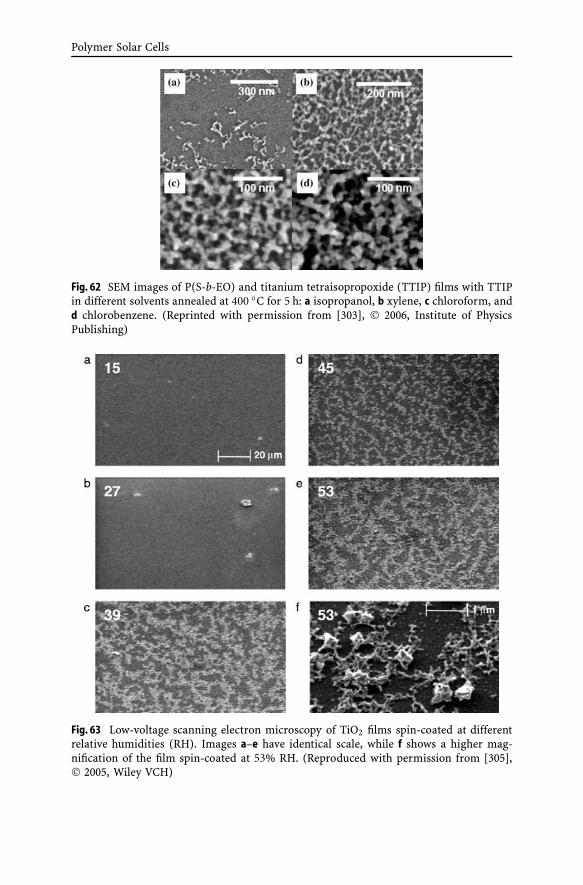
Polymer Solar Cells
Fig. 62 SEM images of P(S-b-EO) and titanium tetraisopropoxide (TTIP) films with TTIPin different solvents annealed at 400 ◦C for 5 h: a isopropanol, b xylene, c chloroform, andd chlorobenzene. (Reprinted with permission from [303], © 2006, Institute of PhysicsPublishing)
Fig. 63 Low-voltage scanning electron microscopy of TiO2 films spin-coated at differentrelative humidities (RH). Images a–e have identical scale, while f shows a higher mag-nification of the film spin-coated at 53% RH. (Reproduced with permission from [305],© 2005, Wiley VCH)

H. Hoppe · N.S. Sariciftci
of the TiO2 in the blends as a bottleneck for electron transport through thedevice.
Another interesting approach to form P3HT/TiO2 bulk heterojunctionswas proposed by Feng et al. [306]. They used ultrasonic-assisted polymeriza-tion of 3-hexylthiophene directly into dispersed TiO2 nanocrystals in chlo-roform, followed by spin casting of thin films. The authors achieved morehomogeneous films by increasing the weight fraction of TiO2 to an optimalratio of 50%. Absorption spectra indicate a rather ordered polymer structureon top of the nanocrystals leading to improved charge generation.
5Carbon Nanotubes in Polymer Solar Cells
Since their discovery in 1991, carbon nanotubes (CNTs) have been a constantsource of scientific inspiration [307]. Among the most intriguing propertiesof CNTs is the electric field enhanced electron emission from the nano-tubes [308]. Initial studies combining CNTs and conjugated polymers con-centrated on the diode properties in a CNT–polymer heterojunction [309].Romero et al. demonstrated light-sensitive photodetectors in combinationwith a PPV derivative. The authors showed that hole injection from the CNTelectrode proved to be much more efficient than using an ITO electrode, andrelated this phenomenon to the enhancement of the local electric field at thetip of the nanotubes [309].
Curran et al. demonstrated the use of multiwalled carbon nanotubes(MWNTs) to increase the conductivity within PPV films. Blending about15% (by mass) CNTs into the PPV films yielded improvements of five ordersof magnitude and was accompanied by a reduction in photoluminescenceefficiency [310].
The application of MWNTs in the field of polymer solar cells was pre-sented by Ago et al. [311]. Here, a layer of CNTs served as a replacementfor the common ITO hole-collecting electrode in a single layer PPV/Aldiode (Fig. 64). The authors related the twofold enhancement of the EQEobserved with the MWNT based device to the formation of a complex net-work with an increased interface area between MWNTs and PPV, in add-ition to a stronger built-in electric field as a result of the higher workfunction of MWNTs compared to the standard ITO electrode [311, 312]. Todetermine whether electron or energy transfer processes dominate withinMWNT:PPV blends, their photophysical properties were studied by photolu-minescence and PIA spectroscopy. The results confirmed nonradiative energytransfer from PPV singlet excitons to the MWNTs as the main electronicinteraction [313].
The first single-walled carbon nanotube (SWNT)–conjugated polymerphotovoltaic devices were presented by Kymakis et al. [314]. As photoactive

Polymer Solar Cells
Fig. 64 a SEM micrograph of the surface of a spin-coated MWNT film. b The cleavedsurface of a PPV±MWNT composite near the bottom of the MWNT layer. The small par-ticles seen in the composite are evaporated gold particles used to avoid a charging effectbecause the composite is less conducting than the pure MWNT film. (Reproduced withpermission from [311], © 1999, Wiley VCH)
layer a blend of P3OT with a low SWNT concentration (< 1% by weight) wassandwiched between an ITO and an aluminum electrode. Thereby the CNT–P3OT junctions acted as dissociation centers for excitons on the polymer,enabling efficient transport of electrons via the nanotubes to the metal elec-trode [314]. The power conversion efficiency increased in comparison to thepristine polymer film by about three orders of magnitude. The observationof a relatively high open circuit voltage (VOC) of 0.75 V was attributed to theformation of ohmic contacts between the CNTs and the metal electrode, re-sulting in a weak dependence of VOC on the metal electrode used [315]. Whiledye functionalization of CNTs yielded a relative increase of the observedphotocurrent [316], the application of PEDOT:PSS modified ITO electrodes
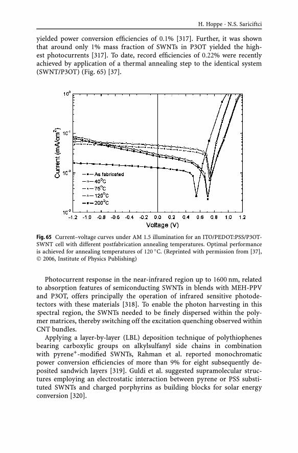
H. Hoppe · N.S. Sariciftci
yielded power conversion efficiencies of 0.1% [317]. Further, it was shownthat around only 1% mass fraction of SWNTs in P3OT yielded the high-est photocurrents [317]. To date, record efficiencies of 0.22% were recentlyachieved by application of a thermal annealing step to the identical system(SWNT/P3OT) (Fig. 65) [37].
Fig. 65 Current–voltage curves under AM 1.5 illumination for an ITO/PEDOT:PSS/P3OT-SWNT cell with different postfabrication annealing temperatures. Optimal performanceis achieved for annealing temperatures of 120 ◦C. (Reprinted with permission from [37],© 2006, Institute of Physics Publishing)
Photocurrent response in the near-infrared region up to 1600 nm, relatedto absorption features of semiconducting SWNTs in blends with MEH-PPVand P3OT, offers principally the operation of infrared sensitive photode-tectors with these materials [318]. To enable the photon harvesting in thisspectral region, the SWNTs needed to be finely dispersed within the poly-mer matrices, thereby switching off the excitation quenching observed withinCNT bundles.
Applying a layer-by-layer (LBL) deposition technique of polythiophenesbearing carboxylic groups on alkylsulfanyl side chains in combinationwith pyrene+-modified SWNTs, Rahman et al. reported monochromaticpower conversion efficiencies of more than 9% for eight subsequently de-posited sandwich layers [319]. Guldi et al. suggested supramolecular struc-tures employing an electrostatic interaction between pyrene or PSS substi-tuted SWNTs and charged porphyrins as building blocks for solar energyconversion [320].
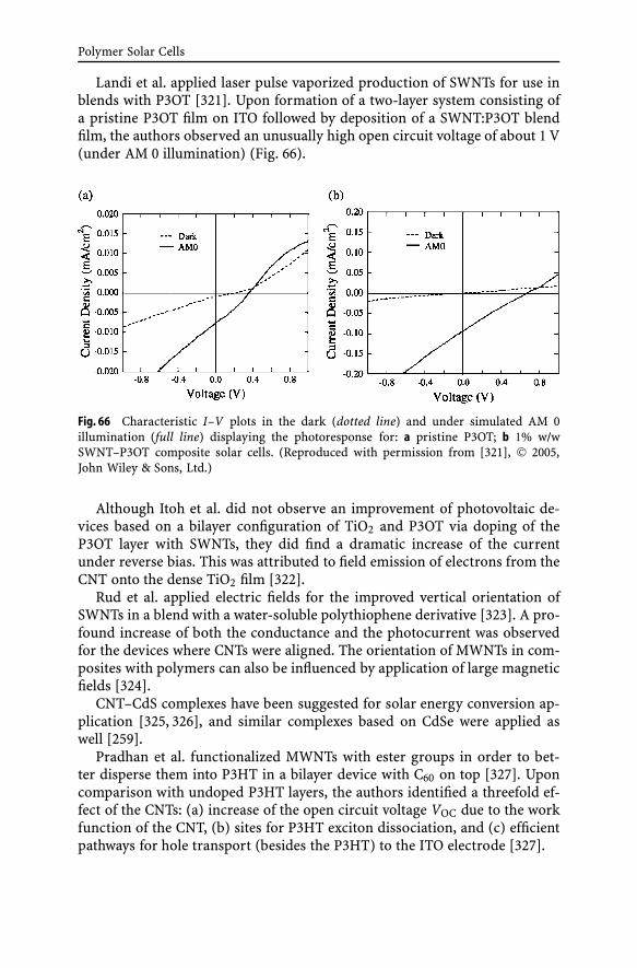
Polymer Solar Cells
Landi et al. applied laser pulse vaporized production of SWNTs for use inblends with P3OT [321]. Upon formation of a two-layer system consisting ofa pristine P3OT film on ITO followed by deposition of a SWNT:P3OT blendfilm, the authors observed an unusually high open circuit voltage of about 1 V(under AM 0 illumination) (Fig. 66).
Fig. 66 Characteristic I–V plots in the dark (dotted line) and under simulated AM 0illumination (full line) displaying the photoresponse for: a pristine P3OT; b 1% w/wSWNT–P3OT composite solar cells. (Reproduced with permission from [321], © 2005,John Wiley & Sons, Ltd.)
Although Itoh et al. did not observe an improvement of photovoltaic de-vices based on a bilayer configuration of TiO2 and P3OT via doping of theP3OT layer with SWNTs, they did find a dramatic increase of the currentunder reverse bias. This was attributed to field emission of electrons from theCNT onto the dense TiO2 film [322].
Rud et al. applied electric fields for the improved vertical orientation ofSWNTs in a blend with a water-soluble polythiophene derivative [323]. A pro-found increase of both the conductance and the photocurrent was observedfor the devices where CNTs were aligned. The orientation of MWNTs in com-posites with polymers can also be influenced by application of large magneticfields [324].
CNT–CdS complexes have been suggested for solar energy conversion ap-plication [325, 326], and similar complexes based on CdSe were applied aswell [259].
Pradhan et al. functionalized MWNTs with ester groups in order to bet-ter disperse them into P3HT in a bilayer device with C60 on top [327]. Uponcomparison with undoped P3HT layers, the authors identified a threefold ef-fect of the CNTs: (a) increase of the open circuit voltage VOC due to the workfunction of the CNT, (b) sites for P3HT exciton dissociation, and (c) efficientpathways for hole transport (besides the P3HT) to the ITO electrode [327].
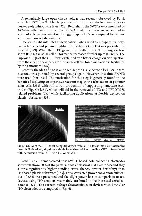
H. Hoppe · N.S. Sariciftci
A remarkably large open circuit voltage was recently observed by Patyket al. for P3OT:SWNT blends prepared on top of an electrochemically de-posited polybithiophene layer [328]. Beforehand the SWNTs were modified by2-(2-thienyl)ethanol groups. Use of Ca/Al metal back electrodes resulted ina remarkable enhancement of the VOC of up to 1.8 V as compared to the barealuminum contact showing 1 V.
Deeper insight into CNT functionalities when used as a dopant for poly-mer solar cells and polymer light-emitting diodes (PLEDs) was presented byXu et al. [329]. While the PLED gained from rather low CNT doping levels ofabout 0.02%, the solar cell performance increased further up to 0.2 wt %. Theimproved EQE of the OLED was explained by a better charge carrier injectionfrom the electrode, whereas for the solar cell exciton dissociation is facilitatedby the nanotubes [329].
Recently the idea of Ago et al. to replace the ITO electrode by a CNT basedelectrode was pursued by several groups again. However, this time SWNTswere used [330–333]. The motivation for this step is generally found in thebenefit of replacing an expensive vacuum step in the fabrication of polymersolar cells [330] with roll-to-roll production of supporting nanotube elec-trodes (Fig. 67) [331], which will aid in the removal of ITO and PEDOT:PSSrelated problems [332] while facilitating applications of flexible devices onplastic substrates [333].
Fig. 67 a SEM of the CNT sheet being dry drawn from a CNT forest into a self-assembledsheet. b Undensified, dry-drawn single layer sheet of free standing CNTs. (Reproducedwith permission from [331], © 2006, Wiley-VCH)
Rowell et al. demonstrated that SWNT based hole-collecting electrodesshow well above 80% of the performance of classical ITO electrodes, and theyallow a significantly higher bending stress (hence, greater flexibility) thanITO based plastic substrates [333]. Thus, corrected power conversion efficien-cies of 2.5% were presented and the slight power loss in comparison to testdevices using ITO contacts was mainly attributed to the increased serial re-sistance [333]. The current–voltage characteristics of devices with SWNT orITO electrodes are compared in Fig. 68.
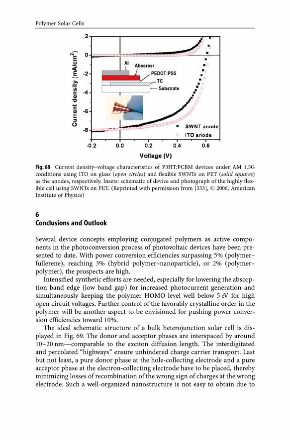
Polymer Solar Cells
Fig. 68 Current density–voltage characteristics of P3HT:PCBM devices under AM 1.5Gconditions using ITO on glass (open circles) and flexible SWNTs on PET (solid squares)as the anodes, respectively. Insets: schematic of device and photograph of the highly flex-ible cell using SWNTs on PET. (Reprinted with permission from [333], © 2006, AmericanInstitute of Physics)
6Conclusions and Outlook
Several device concepts employing conjugated polymers as active compo-nents in the photoconversion process of photovoltaic devices have been pre-sented to date. With power conversion efficiencies surpassing 5% (polymer–fullerene), reaching 3% (hybrid polymer–nanoparticle), or 2% (polymer–polymer), the prospects are high.
Intensified synthetic efforts are needed, especially for lowering the absorp-tion band edge (low band gap) for increased photocurrent generation andsimultaneously keeping the polymer HOMO level well below 5 eV for highopen circuit voltages. Further control of the favorably crystalline order in thepolymer will be another aspect to be envisioned for pushing power conver-sion efficiencies toward 10%.
The ideal schematic structure of a bulk heterojunction solar cell is dis-played in Fig. 69. The donor and acceptor phases are interspaced by around10–20 nm—comparable to the exciton diffusion length. The interdigitatedand percolated “highways” ensure unhindered charge carrier transport. Lastbut not least, a pure donor phase at the hole-collecting electrode and a pureacceptor phase at the electron-collecting electrode have to be placed, therebyminimizing losses of recombination of the wrong sign of charges at the wrongelectrode. Such a well-organized nanostructure is not easy to obtain due to
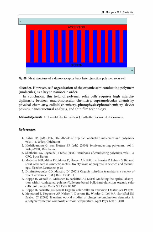
H. Hoppe · N.S. Sariciftci
Fig. 69 Ideal structure of a donor–acceptor bulk heterojunction polymer solar cell
disorder. However, self-organization of the organic semiconducting polymers(molecules) is a key to nanoscale order.
In conclusion, this field of polymer solar cells requires high interdis-ciplinarity between macromolecular chemistry, supramolecular chemistry,physical chemistry, colloid chemistry, photophysics/photochemistry, devicephysics, nanostructural analysis, and thin film technology.
Acknowledgements HH would like to thank A.J. Ledbetter for useful discussions.
References
1. Nalwa HS (ed) (1997) Handbook of organic conductive molecules and polymers,vols 1–4. Wiley, Chichester
2. Hadziioannou G, van Hutten PF (eds) (2000) Semiconducting polymers, vol 1.Wiley-VCH, Weinheim
3. Skotheim TA, Reynolds JR (eds) (2006) Handbook of conducting polymers, vols 1–2.CRC, Boca Raton
4. McGehee MD, Miller EK, Moses D, Heeger AJ (1999) In: Bernier P, Lefrant S, Bidan G(eds) Advances in synthetic metals: twenty years of progress in science and technol-ogy. Elsevier, Lausanne, p 98
5. Dimitrakopoulos CD, Mascaro DJ (2001) Organic thin-film transistors: a review ofrecent advances. IBM J Res Dev 45:11
6. Hoppe H, Arnold N, Meissner D, Sariciftci NS (2003) Modeling the optical absorp-tion within conjugated polymer/fullerene-based bulk-heterojunction organic solarcells. Sol Energy Mater Sol Cells 80:105
7. Hoppe H, Sariciftci NS (2004) Organic solar cells: an overview. J Mater Res 19:19248. Montanari I, Nogueira AF, Nelson J, Durrant JR, Winder C, Loi MA, Sariciftci NS,
Brabec CJ (2001) Transient optical studies of charge recombination dynamics ina polymer/fullerene composite at room temperature. Appl Phys Lett 81:3001
Polymer Solar Cells
9. Nogueira AF, Montari I, Nelson J, Durrant JR, Winder C, Sariciftci NS, Brabec C(2003) Charge recombination in conjugated polymer/fullerene blended films studiedby transient absorption spectroscopy. J Phys Chem B 107:1567
10. Nelson J (2003) Diffusion-limited recombination in polymer–fullerene blends and itsinfluence on photocurrent collection. Phys Rev B 67:155209
11. Sirringhaus H, Brown PJ, Friend RH, Nielsen MM, Bechgaard K, Langeveld-Voss BMW, Spiering AJH, Janssen RAJ, Meijer EW, Herwig P, de Leeuw DM (1999)Two-dimensional charge transport in self-organized, high-mobility conjugated poly-mers. Nature 401:685
12. Singh Th B, Marjanovic N, Matt GJ, Günes S, Sariciftci NS, Montaigne Ramil A, An-dreev A, Sitter H, Schwödiauer R, Bauer S (2004) High-mobility n-channel organicfield-effect transistors based on epitaxially grown C60 films. Org Electron 6:105
13. Brabec CJ, Sariciftci NS, Hummelen JC (2001) Plastic solar cells. Adv Funct Mater11:15
14. Brabec CJ, Dyakonov V, Parisi J, Sariciftci NS (eds) (2003) Organic photovoltaics:concepts and realization, vol 60. Springer, Berlin
15. Brabec CJ (2004) Organic photovoltaics: technology and market. Sol Energy MaterSol Cells 83:273
16. Mozer AJ, Sariciftci NS (2006) In: Skotheim TA, Reynolds JR (eds) Conjugated poly-mers: processing and applications, vol 2. CRC, Boca Raton, p 101
17. Science Citation Index, polymer solar cell(s) (2007) Thompson Scientific, Web ofScience
18. Ma W, Yang C, Gong X, Lee K, Heeger AJ (2005) Thermally stable, efficient polymersolar cells with nanoscale control of the interpenetrating network morphology. AdvFunct Mater 15:1617
19. Reyes-Reyes M, Kim K, Carroll DL (2005) High-efficiency photovoltaic devices basedon annealed poly(3-hexylthiophene) and 1-(3-methoxycarbonyl)-propyl-1-phenyl-(6,6)C61 blends. Appl Phys Lett 87:083506
20. Reyes-Reyes M, Kim K, Dewald J, Lopez R-S, Avadhanula A, Curran S, Carroll DL(2005) Meso-structure formation for enhanced organic photovoltaic cells. Org Lett7:5749
21. Li G, Shrotriya V, Huang J, Yao Y, Moriarty T, Emery K, Yang Y (2005) High-efficiency solution processable polymer photovoltaic cells by self-organization ofpolymer blends. Nat Mater 4:864
22. Karg S, Riess W, Dyakonov V, Schwoerer M (1993) Electrical and optical characteri-zation of poly(phenylene-vinylene) light emitting diodes. Synth Met 54:427
23. Yu G, Zhang C, Heeger AJ (1994) Dual-function semiconducting polymer devices:light-emitting and photodetecting diodes. Appl Phys Lett 64:1540
24. Yu G, Pakbaz K, Heeger AJ (1994) Semiconducting polymer diodes: large size, low costphotodetectors with excellent visible–ultraviolet sensitivity. Appl Phys Lett 64:3422
25. Marks RN, Halls JJM, Bradley DDC, Friend RH, Holmes AB (1994) The photovoltaicresponse in poly(p-phenylene vinylene) thin-film devices. J Phys Condens Matter6:1379
26. Sariciftci NS, Smilowitz L, Heeger AJ, Wudl F (1992) Photoinduced electron transferfrom a conducting polymer to buckminsterfullerene. Science 258:1474
27. Sariciftci NS, Braun D, Zhang C, Srdanov VI, Heeger AJ, Stucky G, Wudl F (1993)Semiconducting polymer–buckminsterfullerene heterojunctions: diodes, photodi-odes, and photovoltaic cells. Appl Phys Lett 62:585
28. Yu G, Heeger AJ (1995) Charge separation and photovoltaic conversion in polymercomposites with internal donor/acceptor heterojunctions. J Appl Phys 78:4510
H. Hoppe · N.S. Sariciftci
29. Yu G, Gao J, Hummelen JC, Wudl F, Heeger AJ (1995) Polymer photovoltaic cells:enhanced efficiencies via a network of internal donor–acceptor heterojunctions. Sci-ence 270:1789
30. Halls JJM, Walsh CA, Greenham NC, Marseglia EA, Friend RH, Moratti SC,Holmes AB (1995) Efficient photodiodes from interpenetrating polymer networks.Nature 376:498
31. Tada K, Hosada K, Hirohata M, Hidayat R, Kawai T, Onoda M, Teraguchi M, Ma-suda T, Zakhidov AA, Yoshino K (1997) Donor polymer (PAT6)–acceptor polymer(CNPPV) fractal network photocells. Synth Met 85:1305
32. Granström M, Petritsch K, Arias AC, Lux A, Andersson MR, Friend RH (1998) Lam-inated fabrication of polymeric photovoltaic diodes. Nature 395:257
33. Jenekhe SA, Yi S (2000) Efficient photovoltaic cells from semiconducting polymerheterojunctions. Appl Phys Lett 77:2635
34. Shaheen SE, Brabec CJ, Sariciftci NS, Padinger F, Fromherz T, Hummelen JC (2001)25% efficient organic plastic solar cells. Appl Phys Lett 78:841
35. McNeill CR, Abrusci A, Zaumseil J, Wilson R, McKiernan MJ, Burroughes JH,Halls JJM, Greenham NC, Friend RH (2007) Dual electron donor/electron acceptorcharacter of a conjugated polymer in efficient photovoltaic diodes. Appl Phys Lett90:193506
36. Sun B, Greenham NC (2006) Improved efficiency of photovoltaics based on CdSenanorods and poly(3-hexylthiophene) nanofibers. Phys Chem Chem Phys 8:3557
37. Kymakis E, Koudoumas E, Franghiadakis I, Amaratunga GAJ (2006) Post-fabricationannealing effects in polymer–nanotube photovoltaic cells. J Phys D Appl Phys39:1058
38. de Boer B, Stalmach U, van Hutten PF, Melzer C, Krasnikov VV, Hadziioannou G(2001) Supramolecular self-assembly and opto-electronic properties of semiconduct-ing block copolymers. Polymer 42:9097
39. Gratt JA, Cohen RE (2004) The role of ordered block copolymer morphology in theperformance of organic/inorganic photovoltaic devices. J Appl Polym Sci 91:3362–3368
40. Sun S, Fan Z, Wang Y, Haliburton J (2005) Organic solar cell optimizations. J MaterSci 40:1429
41. Heiser T, Adamopoulos G, Brinkmann M, Giovanella U, Ould-Saad S, Brochon C,van de Wetering K, Hadziioannou G (2006) Nanostructure of self-assembled rod–coilblock copolymer films for photovoltaic application. Thin Solid Films 511–512:219
42. Lindner SM, Hüttner S, Chiche A, Thelakkat M, Krausch G (2006) Charge separationat self-assembled nanostructured bulk interface in block copolymers. Angew ChemInt Ed 45:3364–3368
43. Sommer M, Lindner SM, Thelakkat M (2007) Microphase-Separated Donor–AcceptorDiblock Copolymers: Influence of HOMO Energy Levels and Morphology on Poly-mer Solar Cells. Adv Funct Mater 17:1493–1500
44. Halls JJM, Pichler K, Friend RH, Moratti SC, Holmes AB (1996) Exciton diffusionand dissociation in a poly(p-phenylenevinylene)/C60 heterojunction photovoltaiccell. Appl Phys Lett 68:3120
45. Savanije TJ, Warman JM, Goossens A (1998) Visible light sensitisation of titaniumdioxide using a phenylene vinylene polymer. Chem Phys Lett 287:148
46. Pettersson LAA, Roman LS, Inganäs O (1999) Modeling photocurrent action spectraof photovoltaic devices based on organic thin films. J Appl Phys 86:487
47. Haugeneder A, Neges M, Kallinger C, Spirkl W, Lemmer U, Feldmann J, Scherf U,Harth E, Gügel A, Müllen K (1999) Exciton diffusion and dissociation in conjugatedpolymer/fullerene blends and heterostructures. Phys Rev B 59:15346
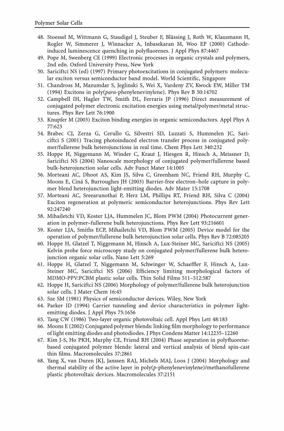
Polymer Solar Cells
48. Stoessel M, Wittmann G, Staudigel J, Steuber F, Blässing J, Roth W, Klausmann H,Rogler W, Simmerer J, Winnacker A, Inbasekaran M, Woo EP (2000) Cathode-induced luminescence quenching in polyfluorenes. J Appl Phys 87:4467
49. Pope M, Swenberg CE (1999) Electronic processes in organic crystals and polymers,2nd edn. Oxford University Press, New York
50. Sariciftci NS (ed) (1997) Primary photoexcitations in conjugated polymers: molecu-lar exciton versus semiconductor band model. World Scientific, Singapore
51. Chandross M, Mazumdar S, Jeglinski S, Wei X, Vardeny ZV, Kwock EW, Miller TM(1994) Excitons in poly(para-phenylenevinylene). Phys Rev B 50:14702
52. Campbell IH, Hagler TW, Smith DL, Ferraris JP (1996) Direct measurement ofconjugated polymer electronic excitation energies using metal/polymer/metal struc-tures. Phys Rev Lett 76:1900
53. Knupfer M (2003) Exciton binding energies in organic semiconductors. Appl Phys A77:623
54. Brabec CJ, Zerza G, Cerullo G, Silvestri SD, Luzzati S, Hummelen JC, Sari-ciftci S (2001) Tracing photoinduced electron transfer process in conjugated poly-mer/fullerene bulk heterojunctions in real time. Chem Phys Lett 340:232
55. Hoppe H, Niggemann M, Winder C, Kraut J, Hiesgen R, Hinsch A, Meissner D,Sariciftci NS (2004) Nanoscale morphology of conjugated polymer/fullerene basedbulk-heterojunction solar cells. Adv Funct Mater 14:1005
56. Morteani AC, Dhoot AS, Kim JS, Silva C, Greenham NC, Friend RH, Murphy C,Moons E, Ciná S, Burroughes JH (2003) Barrier-free electron–hole capture in poly-mer blend heterojunction light-emitting diodes. Adv Mater 15:1708
57. Morteani AC, Sreearunothai P, Herz LM, Phillips RT, Friend RH, Silva C (2004)Exciton regeneration at polymeric semiconductor heterojunctions. Phys Rev Lett92:247240
58. Mihailetchi VD, Koster LJA, Hummelen JC, Blom PWM (2004) Photocurrent gener-ation in polymer–fullerene bulk heterojunctions. Phys Rev Lett 93:216601
59. Koster LJA, Smiths ECP, Mihailetchi VD, Blom PWM (2005) Device model for theoperation of polymer/fullerene bulk heterojunction solar cells. Phys Rev B 72:085205
60. Hoppe H, Glatzel T, Niggemann M, Hinsch A, Lux-Steiner MC, Sariciftci NS (2005)Kelvin probe force microscopy study on conjugated polymer/fullerene bulk hetero-junction organic solar cells. Nano Lett 5:269
61. Hoppe H, Glatzel T, Niggemann M, Schwinger W, Schaeffler F, Hinsch A, Lux-Steiner MC, Sariciftci NS (2006) Efficiency limiting morphological factors ofMDMO-PPV:PCBM plastic solar cells. Thin Solid Films 511–512:587
62. Hoppe H, Sariciftci NS (2006) Morphology of polymer/fullerene bulk heterojunctionsolar cells. J Mater Chem 16:45
63. Sze SM (1981) Physics of semiconductor devices. Wiley, New York64. Parker ID (1994) Carrier tunneling and device characteristics in polymer light-
emitting diodes. J Appl Phys 75:165665. Tang CW (1986) Two-layer organic photovoltaic cell. Appl Phys Lett 48:18366. Moons E (2002) Conjugated polymer blends: linking film morphology to performance
of light emitting diodes and photodiodes. J Phys Condens Matter 14:12235–1226067. Kim J-S, Ho PKH, Murphy CE, Friend RH (2004) Phase separation in polyfluorene-
based conjugated polymer blends: lateral and vertical analysis of blend spin-castthin films. Macromolecules 37:2861
68. Yang X, van Duren JKJ, Janssen RAJ, Michels MAJ, Loos J (2004) Morphology andthermal stability of the active layer in poly(p-phenylenevinylene)/methanofullereneplastic photovoltaic devices. Macromolecules 37:2151
H. Hoppe · N.S. Sariciftci
69. Coakley KM, Liu Y, McGehee MD, Frindell K, Stucky GD (2003) Infiltrating semi-conducting polymers into self-assembled mesoporous titania films for photovoltaicapplications. Adv Funct Mater 13:301
70. Coakley KM, McGehee MD (2003) Photovoltaic cells made from conjugated poly-mers infiltrated into mesoporous titania. Appl Phys Lett 83:3380
71. Coakley KM, McGehee MD (2004) Conjugated polymer photovoltaic cells. ChemMater 16:4533
72. Campbell IH, Rubin S, Zawodzinski TA, Kress JD, Martin RL, Smith DL,Barashkov NN, Ferraris JP (1996) Controlling Schottky energy barriers in organicelectronic devices using self-assembled monolayers. Phys Rev B 54:14321
73. Campbell IH, Kress JD, Martin RL, Smith DL, Barashkov NN, Ferraris JP (1997)Controlling charge injection in organic electronic devices using self-assembledmonolayers. Appl Phys Lett 71:3528
74. Ganzorig C, Matsuda Y, Fujihira M (2002) Chemical modification of indium-tin-oxide electrodes by surface molecular design. Presented at the Materials ResearchSociety meeting, Warrendale. MRS Proc 708:BB3221
75. Lee J, Jung B-J, Lee J-I, Chu HY, Do L-M, Shim H-K (2002) Modification of anITO anode with a hole-transporting SAM for improved OLED device characteristics.J Mater Chem 12:3494
76. Scott JC, Carter SA, Karg S, Angelopoulos M (1997) Polymeric anodes for organiclight-emitting diodes. Synth Met 85:1197
77. Cao Y, Yu G, Zhang C, Menon R, Heeger AJ (1997) Polymer light-emitting diodeswith polyethylene dioxythiophene–polystyrene sulfonate as the transparent anode.Synth Met 87:171
78. Kugler T, Salaneck WR, Rost H, Holmes AB (1999) Polymer band alignment at theinterface with indium tin oxide: consequences for light emitting devices. Chem PhysLett 310:391
79. Greczynski G, Kugler T, Salaneck WR (2000) Energy level alignment in organic-based three-layer structures studied by photoelectron spectroscopy. J Appl Phys88:7187
80. Hung LS, Tang CW, Mason MG (1997) Enhanced electron injection in organic elec-troluminescence devices using an Al/LiF electrode. Appl Phys Lett 70:152
81. Jabbour GE, Kawabe Y, Shaheen SE, Wang JF, Morrell MM, Kippelen B, Peyghambar-ian N (1997) Highly efficient and bright organic electroluminescent devices with analuminum cathode. Appl Phys Lett 71:1762
82. Shaheen SE, Jabbour GE, Morrell MM, Kawabe Y, Kippelen B, Peyghambarian N, Na-bor M-F, Schlaf R, Mash EA, Armstrong NR (1998) Bright blue organic light-emittingdiode with improved color purity using a LiF/Al cathode. J Appl Phys 84:2324
83. Jabbour GE, Kippelen B, Armstrong NR, Peyghambarian N (1998) Aluminum basedcathode structure of enhanced electron injection in electroluminescent organic de-vices. Appl Phys Lett 73:1185
84. Koch N, Pogantsch A, List EJW, Leising G, Blyth RIR, Ramsey MG, Netzer FP (1999)Low-onset organic blue light emitting devices obtained by better interface control.Appl Phys Lett 74:2909
85. Cao Y, Yu G, Parker ID, Heeger AJ (2000) Ultrathin layer alkaline earth metals asstable electron-injection electrodes for polymer light emitting diodes. J Appl Phys88:3618
86. Heil H, Steiger J, Karg S, Gastel M, Ortner H, von Seggern H, Stößel M (2001)Mechanisms of injection enhancements in organic light-emitting diodes through anAl/LiF electrode. J Appl Phys 89:420

Polymer Solar Cells
87. Li F, Feng J, Cheng G, Liu S (2002) Electron injection and electroluminescence in-vestigation of organic light-emitting devices based on a Sn/Al cathode. Synth Met126:347
88. Malliaras GG, Scott JC (1998) The roles of injection and mobility in organic lightemitting diodes. J Appl Phys 83:5399
89. Roman LS, Mammo W, Petterson LAA, Andersson MR, Inganäs O (1998) High quan-tum efficiency polythiophene/C60 photodiodes. Adv Mater 10:774
90. Shaheen SE, Brabec CJ, Sariciftci NS, Jabbour GE (2001) Effects of inserting highlypolar salts between the cathode and active layer of bulk heterojunction photovoltaicdevices. Presented at the Materials Research Society meeting, San Francisco. MRSProc 665:C5511
91. Brabec CJ, Shaheen SE, Winder C, Sariciftci NS, Denk P (2002) Effect of LiF/metalelectrodes on the performance of plastic solar cells. Appl Phys Lett 80:1288
92. Brown TM, Millard IS, Lacey DJ, Burroughes JH, Friend RH, Cacialli F (2001) Theinfluence of LiF thickness on the built-in potential of blue polymer light-emittingdiodes with LiF/Al cathodes. Synth Met 124:15
93. van Gennip WJH, van Duren JKJ, Thüne PC, Janssen RAJ, Niemantsverdriet JW(2002) The interfaces of poly(p-phenylene vinylene) and fullerene derivatives withAl, LiF, and Al/LiF studied by secondary ion mass spectroscopy and X-ray photo-electron spectroscopy: formation of AI/F3 disproved. J Chem Phys 117:5031
94. Deng XY, Tong SW, Hung LS, Mo YQ, Cao Y (2003) Role of ultrathin Alq3 and LiFlayers in conjugated polymer light-emitting diodes. Appl Phys Lett 82:3104
95. Yokoyama T, Yoshimura D, Ito E, Ishii H, Ouchi Y, Seki K (2003) Energy level align-ment at Alq3/LiF/Al interfaces studied by electron spectroscopies: island growth ofLiF and size-dependence of the electronic structures. Jpn J Appl Phys 42:3666
96. Liu J, Duggal AR, Shiang JJ, Heller CM (2004) Efficient bottom cathodes for organiclight-emitting devices. Appl Phys Lett 85:837
97. Jönsson SKM, Carlegrim E, Zhang F, Salaneck WR, Fahlman M (2005) Photoelectronspectroscopy of the contact between the cathode and the active layers in plastic solarcells: the role of LiF. Jpn J Appl Phys 44:3695
98. Gregg BA, Hanna MC (2003) Comparing organic to inorganic photovoltaic cells:theory, experiment, and simulation. J Appl Phys 93:3605
99. Kim H, Jin S-H, Suh H, Lee K (2004) Origin of the open circuit voltage in con-jugated polymer–fullerene photovoltaic cells. In: Kafafi ZH, Lane PA (eds) Organicphotovoltaics IV. SPIE Proc 5215:111
100. Gadisa A, Svensson M, Andersson MR, Inganäs O (2004) Correlation between oxi-dation potential and open-circuit voltage of composite solar cells based on blends ofpolythiophenes/fullerene derivative. Appl Phys Lett 84:1609
101. Hoppe H, Egbe DAM, Mühlbacher D, Sariciftci NS (2004) Photovoltaic action ofconjugated polymer/fullerene bulk heterojunction solar cells using novel PPE-PPVcopolymers. J Mater Chem 14:3461
102. Scharber MC, Mühlbacher D, Koppe M, Denk P, Waldauf C, Heeger AJ, Brabec CJ(2006) Design rules for donors in bulk-heterojunction solar cells—towards 10%energy-conversion efficiency. Adv Mater 18:789
103. Brabec CJ, Cravino A, Meissner D, Sariciftci NS, Fromherz T, Rispens MT, Sanchez L,Hummelen JC (2001) Origin of the open circuit voltage of plastic solar cells. AdvFunct Mater 11:374
104. Kooistra FB, Knol J, Kastenberg F, Popescu LM, Verhees WJH, Kroon JM, Humme-len JC (2007) Increasing the open circuit voltage of bulk-heterojunction solar cellsby raising the LUMO level of the acceptor. Org Lett 9:551
H. Hoppe · N.S. Sariciftci
105. Mihailetchi VD, Blom PWM, Hummelen JC, Rispens MT (2003) Cathode depen-dence of the open-circuit voltage of polymer: fullerene bulk heterojunction solarcells. J Appl Phys 94:6849
106. Heller CM, Campbell IH, Smith DL, Barashkov NN, Ferraris JP (1997) Chemicalpotential pinning due to equilibrium electron transfer at metal/C60-doped polymerinterfaces. J Appl Phys 81:3227
107. Hirose Y, Kahn A, Aristov V, Soukiassian P, Bulovic V, Forrest SR (1996) Chemistryand electronic properties of metal–organic semiconductor interfaces: Al, Ti, In, Sn,Ag, and Au on PTCDA. Phys Rev B 54:13748
108. Ishii H, Sugiyama K, Ito E, Seki K (1999) Energy level alignment and interfacial elec-tronic structures at organic/metal and organic/organic interfaces. Adv Mater 11:605
109. Yan L, Gao Y (2002) Interfaces in organic semiconductor devices. Thin Solid Films417:101
110. Koch N, Kahn A, Ghijsen J, Pireaux J-J, Schwartz J, Johnson RL, Elschner A (2003)Conjugated organic molecules on metal versus polymer electrodes: demonstrationof a key energy level alignment mechanism. Appl Phys Lett 82:70
111. Cahen D, Kahn A (2003) Electron energetics at surfaces and interfaces: concepts andexperiments. Adv Mater 15:271
112. Veenstra SC, Jonkman HT (2003) Energy-level alignment at metal–organic andorganic–organic interfaces. J Polym Sci Polym Phys 41:2549
113. Veenstra SC, Heeres A, Hadziioannou G, Sawatzky GA, Jonkman HT (2002) Oninterface dipole layers between C60 and Ag or Au. Appl Phys A 75:661
114. Melzer C, Krasnikov VV, Hadziioannou G (2003) Organic donor/acceptor photo-voltaics: the role of C60/metal interfaces. Appl Phys Lett 82:3101
115. van Duren JKJ, Loos J, Morrissey F, Leewis CM, Kivits KPH, van IJzendoorn LJ,Rispens MT, Hummelen JC, Janssen RAJ (2002) In-situ compositional and structuralanalysis of plastic solar cells. Adv Funct Mater 12:665
116. Bulle-Lieuwma CWT, van Gennip WJH, van Duren JKJ, Jonkheijm P, Janssen RAJ,Niemantsverdriet JW (2003) Characterization of polymer solar cells by TOF-SIMSdepth profiling. Appl Surf Sci 203–204:547
117. Gao J, Hide F, Wang H (1997) Efficient photodetectors and photovoltaic cells fromcomposites of fullerenes and conjugated polymers: photoinduced electron transfer.Synth Met 84:979
118. Liu J, Shi Y, Yang Y (2001) Solvation-induced morphology effects on the perform-ance of polymer-based photovoltaic devices. Adv Funct Mater 11:420
119. Scharber MC, Schulz NA, Sariciftci NS, Brabec CJ (2003) Optical- and photocurrent-detected magnetic resonance studies on conjugated polymer/fullerene composites.Phys Rev B 67:085202
120. van Duren JKJ, Yang X, Loos J, Bulle-Lieuwma CWT, Sieval AB, Hummelen JC,Janssen RAJ (2004) Relating the morphology of poly(p-phenylene vinylene)/meth-anofullerene blends to solar-cell performance. Adv Funct Mater 14:425
121. Riedel I, von Hauff E, Parisi J, Martin N, Giacalone F, Dyakonov V (2005)Dimethanofullerenes: new and efficient acceptors in bulk-heterojunction solar cells.Adv Funct Mater 15:1979
122. Katz EA, Faiman D, Tuladhar SM, Kroon JM, Wienk MM, Fromherz T, Padinger F,Brabec CJ, Sariciftci NS (2001) Temperature dependence for the photovoltaic deviceparameters of polymer–fullerene solar cells under operating conditions. J Appl Phys90:5343
123. Dyakonov V (2002) The polymer–fullerene interpenetrating network: one route toa solar cell approach. Physica E 14:53

Polymer Solar Cells
124. Riedel I, Parisi J, Dyakonov V, Lutsen L, Vanderzande D, Hummelen JC (2004)Effect of temperature and illumination on the electrical characteristics of polymer–fullerene bulk-heterojunction solar cells. Adv Funct Mater 14:38
125. Ramsdale CM, Barker JA, Arias AC, MacKenzie JD, Friend RH, Greenham NC (2002)The origin of the open circuit voltage in polyfluorene-based photovoltaic devices.J Appl Phys 92:4266
126. Peumans P, Yakimov A, Forrest SR (2003) Small molecular weight organic thin-filmphotodetectors and solar cells. J Appl Phys 93:3693
127. Schilinsky P, Waldauf C, Hauch J, Brabec CJ (2004) Simulation of light intensitydependent current characteristics of polymer solar cells. J Appl Phys 95:2816
128. Frohne H, Shaheen SE, Brabec CJ, Müller DC, Sariciftci NS, Meerholz K (2002)Influence of the anodic work function on the performance of organic solar cells.ChemPhysChem 9:795
129. Barker JA, Ramsdale CM, Greenham NC (2003) Modeling the current–voltage char-acteristics of bilayer polymer photovoltaic devices. Phys Rev B 67:075205
130. Hummelen JC, Knight BW, LePeq F, Wudl F, Yao J, Wilkins CL (1995) Preparationand characterization of fulleroid and methanofullerene derivatives. J Org Chem60:532
131. Yang CY, Heeger AJ (1996) Morphology of composites of semiconducting polymersmixed with C60. Synth Met 83:85
132. Drees M, Premaratne K, Graupner W, Heflin JR, Davis RM, Marciu D, Miller M(2002) Creation of a gradient polymer–fullerene interface in photovoltaic devices bythermally controlled interdiffusion. Appl Phys Lett 81:1
133. Drees M, Davis RM, Heflin JR (2005) Improved morphology of polymer–fullerenephotovoltaic devices with thermally induced concentration gradients. J Appl Phys97:036103
134. Martens T, D’Haen J, Munters T, Goris L, Beelen Z, Manca J, D’Olieslaeger M, Van-derzande D, Schepper LD, Andriessen R (2002) The influence of the microstructureupon the photovoltaic performance of MDMOPPV:PCBM bulk hetero-junction or-ganic solar cells. Presented at the Materials Research Society Spring Meeting, SanFrancisco. MRS Proc 725:P7111
135. Martens T, D’Haen J, Munters T, Beelen Z, Goris L, Manca J, D’Olieslaeger M, Van-derzande D, Schepper LD, Andriessen R (2003) Disclosure of the nanostructure ofMDMO-PPV:PCBM bulk heterojunction organic solar cells by a combination of SPMand TEM. Synth Met 138:243
136. Martens T, Beelen Z, D’Haen J, Munters T, Goris L, Manca J, D’Olieslaeger M, Van-derzande D, Schepper LD, Andriessen R (2003) Morphology of MDMO-PPV:PCBMbulk hetero-junction organic solar cells studied by AFM, KFM and TEM. In:Kafafi Z H, Fichou D (eds) Organic photovoltaics III. SPIE Proc 4801:40
137. Hoppe H, Drees M, Schwinger W, Schäffler F, Sariciftci NS (2005) Nano-crystallinefullerene phases in polymer/fullerene bulk-heterojunction solar cells: a transmissionelectron microscopy study. Synth Met 152:117
138. McNeill CR, Frohne H, Holdsworth JL, Dastoor PC (2004) Direct influence ofmorphology on current generation in conjugated polymer:methanofullerene solarcells measured by near-field scanning photocurrent microscopy. Synth Met 147:101
139. Geens W, Shaheen SE, Brabec CJ, Poortmans J, Sariciftci NS (2000) Field-effectmobility measurements of conjugated polymer/fullerene photovoltaic blends. Pre-sented at the electronic properties of novel materials—molecular nanostructures,14th international winter school/Euroconference (American Institute of Physics),Kirchberg

H. Hoppe · N.S. Sariciftci
140. Geens W, Shaheen SE, Wessling B, Brabec CJ, Poortmans J, Sariciftci NS (2002)Dependence of field-effect hole mobility of PPV-based polymer films on the spin-casting solvent. Org Electron 3:105
141. Aernouts T, Vanlaeke P, Geens W, Poortmans J, Heremans P, Borghs S, Mertens R(2003) The influence of the donor/acceptor ratio on the performance of organic bulkheterojunction solar cells. Presented at the E-MRS spring meeting, Strasbourg
142. Pacios R, Nelson J, Bradley DDC, Brabec CJ (2003) Composition dependence of elec-tron and hole transport in polyfluorene:[6,6]-phenyl C61-butyric acid methyl esterblend films. Appl Phys Lett 83:4764
143. Melzer C, Koop EJ, Mihailetchi VD, Blom PWM (2004) Hole transport inpoly(phenylene vinylene)/methanofullerene bulk-heterojunction solar cells. AdvFunct Mater 14:865
144. Mihailetchi VD, Koster LJA, Blom PWM, Melzer C, de Boer B, van Duren JKJ, Jans-sen RAJ (2005) Compositional dependence of the performance of poly(p-phenylenevinylene):methanofullerene bulk-heterojunction solar cells. Adv Funct Mater 15:795
145. Dennler G, Mozer AJ, Juska G, Pivrikas A, Österbacka R, Fuchsbauer A, Sariciftci NS(2006) Charge carrier mobility and lifetime versus composition of conjugated poly-mer/fullerene bulk-heterojunction solar cells. Org Electron 7:229
146. Gadisa A, Wang X, Admassie S, Perzon E, Oswald F, Langa F, Andersson MR, In-ganäs O (2006) Stoichiometry dependence of charge transport in polymer/methano-fullerene and polymer/C70 derivative based solar cells. Org Electron 7:195
147. Andersson LM, Inganäs O (2006) Acceptor influence on hole mobility in fullereneblends with alternating copolymers of fluorene. Appl Phys Lett 88:082103
148. Mihailetchi VD, Wildeman J, Blom PWM (2005) Space-charge limited photocurrent.Phys Rev Lett 94:126602
149. Bässler H (1993) Charge transport in disordered organic photoconductors. PhysStatus Solidi B 175:15
150. Dyakonov V (2004) Mechanisms controlling the efficiency of polymer solar cells.Appl Phys A 79:21
151. Riedel I, Dyakonov V (2004) Influence of electronic transport properties ofpolymer–fullerene blends on the performance of bulk heterojunction photovoltaicdevices. Phys Status Solidi A 201:1332
152. Onsager L (1934) Deviations from Ohm’s law in weak electrolytes. J Chem Phys 2:599153. Braun CL (1984) Electric field assisted dissociation of charge transfer states as
a mechanism of photocarrier production. J Chem Phys 80:4157154. Gommans HHP, Kemerink M, Kramer JM, Janssen RAJ (2005) Field and tempera-
ture dependence of the photocurrent in polymer/fullerene bulk heterojunction solarcells. Appl Phys Lett 87:122104
155. Koster LJA, Mihailetchi VD, Ramaker R, Blom PWM (2005) Light intensity de-pendence of open-circuit voltage of polymer:fullerene solar cells. Appl Phys Lett86:123509
156. Koster LJA, Mihailetchi VD, Xie H, Blom PWM (2005) Origin of the light intensitydependence of the short-circuit current of polymer/fullerene solar cells. Appl PhysLett 87:203502
157. Waldauf C, Schilinsky P, Hauch J, Brabec CJ (2004) Material and device concepts fororganic photovoltaics: towards competitive efficiencies. Thin Solid Films 451–452:503
158. Waldauf C, Scharber MC, Schilinsky P, Hauch JA, Brabec CJ (2006) Physics of organicbulk heterojunction devices for photovoltaic applications. J Appl Phys 99:104503
159. Harbecke B (1986) Coherent and incoherent reflection and transmission of multi-layer systems. Appl Phys B 39:165
Polymer Solar Cells
160. Rostalski J, Meissner D (2000) Photocurrent spectroscopy for the investigation ofcharge carrier generation and transport mechanisms in organic p/n-junction solarcells. Sol Energy Mater Sol Cells 63:37
161. Gruber DP, Meinhardt G, Papousek W (2005) Modelling the light absorption inorganic photovoltaic devices. Sol Energy Mater Sol Cells 87:215
162. Niggemann M, Bläsi B, Gombert A, Hinsch A, Hoppe H, Lalanne P, Meissner D,Wittwer V (2002) Trapping light in organic plastic solar cells with integrated diffrac-tion gratings. Presented at the 17th European photovoltaic solar energy conference,Munich, 22–26 October 2001
163. Hoppe H, Arnold N, Meissner D, Sariciftci NS (2004) Modeling of optical absorptionin conjugated polymer/fullerene bulk-heterojunction plastic solar cells. Thin SolidFilms 451–452:589
164. Persson N-K, Schubert M, Inganäs O (2004) Optical modelling of a layered photo-voltaic device with a polyfluorene derivative/fullerene as the active layer. Sol EnergyMater Sol Cells 83:169
165. Hoppe H, Shokhovets S, Gobsch G (2007) Inverse relation between photocurrent andabsorption layer thickness in polymer solar cells. Phys Status Solidi RRL 1:R40
166. Slooff LH, Veenstra SC, Kroon JM, Moet DJD, Sweelssen J, Koetse MM (2007) De-termining the internal quantum efficiency of highly efficient polymer solar cellsthrough optical modeling. Appl Phys Lett 90:143506
167. Lutsen L, Adriaensens P, Becker H, van Breemen AJ, Vanderzande D, Gelan J (1999)New synthesis of a soluble high molecular weight poly(arylene vinylene): poly[2-methoxy-5-(3,7-dimethyloctyloxy)-p-phenylene vinylene] polymerization and de-vice properties. Macromolecules 32:6517
168. Munters T, Martens T, Goris L, Vrindts V, Manca J, Lutsen L, Ceunick WD, Van-derzande D, Schepper LD, Gelan J, Sariciftci NS, Brabec CJ (2002) A comparisonbetween state-of-the-art gilch and sulphinyl synthesised MDMO-PPV/PCBM bulkhetero-junction solar cells. Thin Solid Films 403–404:247
169. Mozer A, Denk P, Scharber M, Neugebauer H, Sariciftci NS, Wagner P, Lutsen L,Vanderzande D (2004) Novel regiospecific MDMO-PPV copolymer with improvedcharge transport for bulk heterojunction solar cells. J Phys Chem B 108:5235
170. Wienk MM, Kroon JM, Verhees WJH, Knol J, Hummelen JC, van Hall PA,Janssen RAJ (2003) Efficient methano[70]fullerene/MDMO-PPV bulk heterojunctionphotovoltaic cells. Angew Chem Int Ed 42:3371
171. Camaioni N, Ridolfi G, Casalbore-Miceli G, Possamai G, Maggini M (2002) The effectof a mild thermal treatment on the performance of poly(3-alkylthiophene)/fullerenesolar cells. Adv Mater 14:1735
172. Padinger F, Rittberger RS, Sariciftci NS (2003) Effects of postproduction treatmenton plastic solar cells. Adv Funct Mater 13:1
173. Zhao Y, Yuan GX, Roche P, Leclerc M (1995) A calorimetric study of the phasetransitions in poly(3-hexylthiophene). Polymer 36:2211
174. Berggren M, Gustafsson G, Inganäs O, Andersson MR, Wennerström O, Hjertberg T(1994) Thermal control of near-infrared and visible electroluminescence in alkyl-phenyl substituted polythiophenes. Appl Phys Lett 65:1489
175. Chirvase D, Parisi J, Hummelen JC, Dyakonov V (2004) Influence of nanomorphol-ogy on the photovoltaic action of polymer–fullerene composites. Nanotechnology15:1317
176. Brown PJ, Thomas DS, Köhler A, Wilson J, Kim JS, Ramsdale C, Sirringhaus H,Friend RH (2003) Effect of interchain interactions on the absorption and emissionof poly(3-hexylthiophene). Phys Rev B 67:064203

H. Hoppe · N.S. Sariciftci
177. Ahn T, Lee H, Han S-H (2002) Effect of annealing of polythiophene derivative forpolymer light-emitting diodes. Appl Phys Lett 80:392
178. Kim Y, Choulis SA, Nelson J, Bradley DDC, Cook S, Durrant JR (2005) De-vice annealing effect in organic solar cells with blends of regioregular poly(3-hexylthiophene) and soluble fullerene. Appl Phys Lett 86:063502
179. Yang X, Loos J, Veenstra SC, Verhees WJH, Wienk MM, Kroon JM, Michels MAJ,Janssen RAJ (2005) Nanoscale morphology of high-performance polymer solar cells.Nano Lett 5:579
180. Ihn KJ, Moulton J, Smith P (1993) Whiskers of poly(3-alkylthiophene)s. J PolymSci B Polym Phys 31:735
181. Erb T, Zhokhavets U, Gobsch G, Raleva S, Stühn B, Schilinsky P, Waldauf C,Brabec CJ (2005) Correlation between structural and optical properties of compositepolymer films for organic solar cells. Adv Funct Mater 15:1193
182. Erb T, Zhokhavets U, Hoppe H, Gobsch G, Al-Ibrahim M, Ambacher O (2006) Ab-sorption and crystallinity of poly(3-hexylthiophene)/fullerene blends in dependenceon annealing temperature. Thin Solid Films 511–512:483
183. Zhokhavets U, Erb T, Gobsch G, Al-Ibrahim M, Ambacher O (2006) Relation be-tween absorption and crystallinity of poly(3-hexylthiophene)/fullerene films forplastic solar cells. Chem Phys Lett 418:343
184. Yang X, van Duren JKJ, Rispens MT, Hummelen JC, Janssen RAJ, Michels MAJ,Loos J (2004) Crystalline organization of a methanofullerene as used for plasticsolar-cell applications. Adv Mater 16:802
185. Schuller S, Schilinsky P, Hauch J, Brabec CJ (2004) Determination of the degradationconstant of bulk heterojunction solar cells by accelerated lifetime measurements.Appl Phys A Mater Sci Proc 79:37
186. Drees M, Hoppe H, Winder C, Neugebauer H, Sariciftci NS, Schwinger W, Schäffler F,Topf C, Scharber MC, Zhu Z, Gaudiana R (2005) Stabilization of the nanomorphol-ogy of polymer/fullerene bulk heterojunction blends using a novel polymerizablefullerene derivative. J Mater Chem 15:5158
187. Sivula K, Ball ZT, Watanabe N, Fréchet JMJ (2006) Amphiphilic diblock copolymercompatibilizers and their effect on the morphology and performance of polythio-phene:fullerene solar cells. Adv Mater 18:206
188. Brabec CJ, Hauch JA, Schilinsky P, Waldauf C (2005) Production aspects of organicphotovoltaics and their impact on the commercialization of devices. MRS Bull 30:50
189. Huang J, Li G, Yang Y (2005) Influence of composition and heat-treatment on thecharge transport properties of poly(3-hexylthiophene) and [6,6]-phenyl C61-butyricacid methyl ester blends. Appl Phys Lett 87:112105
190. Kim Y, Cook S, Tuladhar SM, Choulis SA, Nelson J, Durrant JR, Bradley DDC,Giles M, McCulloch I, Ha C-S, Ree M (2006) A strong regioregularity effect in self-organizing conjugated polymer films and high-efficiency polythiophene:fullerenesolar cells. Nat Mater 5:197
191. Li G, Shrotriya V, Yao Y, Yang Y (2005) Investigation of annealing effects andfilm thickness dependence of polymer solar cells based on poly(3-hexylthiophene).J Appl Phys 98:043704
192. Moulé AJ, Bonekamp JB, Meerholz K (2006) The effect of active layer thicknessand composition on the performance of bulk-heterojunction solar cells. J Appl Phys100:094503
193. Schilinsky P, Asawapirom U, Scherf U, Biele M, Brabec CJ (2005) Influence of the mo-lecular weight of poly(3-hexylthiophene) on the performance of bulk heterojunctionsolar cells. Chem Mater 17:2175

Polymer Solar Cells
194. Schilinsky P, Waldauf C, Brabec CJ (2002) Recombination and loss analysis in poly-thiophene based bulk heterojunction photodetectors. Appl Phys Lett 81:3885
195. Svensson M, Zhang F, Veenstra SC, Verhees WJH, Hummelen JC, Kroon JM,Inganäs O, Andersson MR (2003) High-performance polymer solar cells ofan alternating polyfluorene copolymer and a fullerene derivative. Adv Mater15:988
196. Yohannes T, Zhang F, Svensson M, Hummelen JC, Andersson MR, Inganäs O (2004)Polyfluorene copolymer based bulk heterojunction solar cells. Thin Solid Films 449:152
197. Zhang F, Jespersen KG, Björström C, Svensson M, Andersson MR, Sundström V,Magnusson K, Moons E, Yartsev A, Inganäs O (2006) Influence of solvent mixingon the morphology and performance of solar cells based on polyfluorene copoly-mer/fullerene blends. Adv Funct Mater 16:667
198. Roncali J (1997) Synthetic principles for band gap control in linear π-conjugatedsystems. Chem Rev 97:173
199. Winder C, Sariciftci NS (2004) Low bandgap polymers for photon harvesting in bulkheterojunction solar cells. J Mater Chem 14:1077
200. Thompson BC, Kim Y-G, Reynolds JR (2005) Spectral broadening in MEH-PPV:PCBM-based photovoltaic devices via blending with narrow band gapcyanovinylene-dioxythiophene polymer. Macromolecules 38:5359
201. Dhanabalan A, Knol J, Hummelen JC, Janssen RAJ (2001) Design and synthesis ofnew processible donor–acceptor dyad and triads. Synth Met 119:519
202. van Duren JKJ, Dhanabalan A, van Hal PA, Janssen RAJ (2001) Low-bandgap poly-mer photovoltaic cells. Synth Met 121:1587
203. Brabec CJ, Winder C, Sariciftci NS, Hummelen JC, Dhanabalan A, van Hal PA,Janssen RAJ (2002) A low-bandgap semiconducting polymer for photovoltaic de-vices and infrared emitting diodes. Adv Funct Mater 12:709
204. Colladet K, Nicolas M, Goris L, Lutsen L, Vanderzande D (2004) Low-band gappolymers for photovoltaic applications. Thin Solid Films 451–452:7
205. Zhou Q, Hou Q, Zheng L, Deng X, Yu G, Cao Y (2004) Fluorene-based low band-gapcopolymers for high performance. Appl Phys Lett 84:1653
206. Campos LM, Tontcheva A, Günes S, Sonmez G, Neugebauer H, Sariciftci NS, Wudl F(2005) Extended photocurrent spectrum of a low band gap polymer in a bulk het-erojunction solar cell. Chem Mater 17:4031
207. Wang X, Perzon E, Delgado JL, de la Cruz P, Zhang F, Langa F, Andersson M, In-ganäs O (2004) Infrared photocurrent spectral response from plastic solar cell withlow-bandgap polyfluorene and fullerene derivative. Appl Phys Lett 85:5081
208. Wang X, Perzon E, Oswald F, Langa F, Admassie S, Andersson MR, Inganäs O (2005)Enhanced photocurrent spectral response in low-bandgap polyfluorene and C70-derivative-based solar cells. Adv Funct Mater 15:1665
209. Perzon E, Wang X, Zhang F, Mammo W, Delgado JL, de la Cruz P, Inganäs O,Langa F, Andersson MR (2005) Design, synthesis and properties of low-bandgappolyfluorenes for photovoltaic devices. Synth Met 154:53
210. Wang X, Perzon E, Mammo W, Oswald F, Admassie S, Persson N-K, Langa F, Ander-sson MR, Inganäs O (2006) Polymer solar cells with low-bandgap polymers blendedwith C70-derivative give photocurrent at 1 µm. Thin Solid Films 511–512:576
211. Perzon E, Wang X, Admassie S, Inganäs O, Andersson MR (2006) An alternating lowband-gap polyfluorene for optoelectronic devices. Polymer 47:4261
212. Zhang F, Perzon E, Wang X, Mammo W, Andersson MR, Inganäs O (2005) Polymersolar cells based on a low-bandgap fluorene copolymer and a fullerene derivativewith photocurrent extended to 850 nm. Adv Funct Mater 15:745
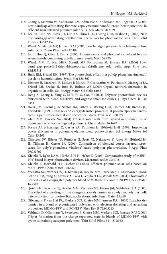
H. Hoppe · N.S. Sariciftci
213. Zhang F, Mammo W, Andersson LM, Admassie S, Andersson MR, Inganäs O (2006)Low-bandgap alternating fluorene copolymer/methanofullerene heterojunctions inefficient near-infrared polymer solar cells. Adv Mater 18:2169
214. Lee SK, Cho NS, Kwak JH, Lim KS, Shim H-K, Hwang D-H, Brabec CJ (2006) Newlow band-gap alternating polyfluorene derivatives for photovoltaic cells. Thin SolidFilms 511–512:157
215. Wienk M, Struijk MP, Janssen RAJ (2006) Low bandgap polymer bulk heterojunctionsolar cells. Chem Phys Lett 422:488
216. Iou J, Hou Q, Chen J, Cao Y (2006) Luminescence and photovoltaic cells of benzo-selenadiazole-containing polyfluorenes. Synth Met 156:470
217. Wienk MM, Turbiez MGR, Struijk MP, Fonrodona M, Janssen RAJ (2006) Low-band gap poly(di-2-thienylthienopyrazine):fullerene solar cells. Appl Phys Lett88:153511
218. Halls JJM, Friend RH (1997) The photovoltaic effect in a poly(p-phenylenevinylene)/perylene heterojunction. Synth Met 85:1307
219. Dittmer JJ, Lazzaroni R, Leclere P, Moretti P, Granström M, Petritsch K, Marseglia EA,Friend RH, Bredas JL, Rost H, Holmes AB (2000) Crystal network formation inorganic solar cells. Sol Energy Mater Sol Cells 61:53
220. Deng X, Zheng L, Yang C, Li Y, Yu G, Cao Y (2004) Polymer photovoltaic devicesfabricated with blend MEHPPV and organic small molecules. J Phys Chem B 108:3451
221. Halls JJM, Cornil J, de Santos DA, Silbey R, Hwang D-H, Holmes AB, Brédas JL,Friend RH (1999) Charge- and energy-transfer processes at polymer/polymer inter-faces: a joint experimental and theoretical study. Phys Rev B 60:5721
222. Alam MM, Jenekhe SA (2004) Efficient solar cells from layered nanostructures ofdonor and acceptor conjugated polymers. Chem Mater 16:4647
223. Breeze AJ, Schlesinger Z, Carter SA, Tillmann H, Hörhold H-H (2004) Improvingpower efficiencies in polymer–polymer blend photovoltaics. Sol Energy Mater SolCells 83:263
224. Chasteen SV, Härter JO, Rumbles G, Scott JC, Nakazawa Y, Jones M, Hörhold H-H, Tillman H, Carter SA (2006) Comparison of blended versus layered struc-tures for poly(p-phenylene vinylene)-based polymer photovoltaics. J Appl Phys99:033709
225. Kietzke T, Egbe DAM, Hörhold H-H, Neher D (2006) Comparative study of M3EH-PPV-based bilayer photovoltaic devices. Macromolecules 39:4018
226. Kietzke T, Hörhold H-H, Neher D (2005) Efficient polymer solar cells based onM3EH-PPV. Chem Mater 17:6532
227. Veenstra SC, Verhees WJH, Kroon JM, Koetse MM, Sweelssen J, Bastiaansen JJAM,Schoo HFM, Yang X, Alexeev A, Loos J, Schubert US, Wienk MM (2004) Photovoltaicproperties of a conjugated polymer blend of MDMO-PPV and PCNEPV. Chem Mater16:2503
228. Quist PAC, Savenije TJ, Koetse MM, Veenstra SC, Kroon JM, Siebbeles LDA (2005)The effect of annealing on the charge-carrier dynamics in a polymer/polymer bulkheterojunction for photovoltaic applications. Adv Funct Mater 15:469
229. Offermans T, van Hal PA, Meskers SCJ, Koetse MM, Janssen RAJ (2005) Exciplex dy-namics in a blend of p-conjugated polymers with electron donating and acceptingproperties: MDMO-PPV and PCNEPV. Phys Rev B 72:045213
230. Veldman D, Offermans T, Sweelssen J, Koetse MM, Meskers SCJ, Janssen RAJ (2006)Triplet formation from the charge-separated state in blends of MDMO-PPV withcyano-containing acceptor polymers. Thin Solid Films 511–512:333
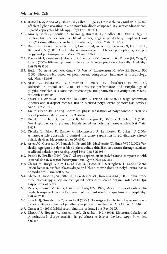
Polymer Solar Cells
231. Russell DM, Arias AC, Friend RH, Silva C, Ego C, Grimsdale AC, Müllen K (2002)Efficient light harvesting in a photovoltaic diode composed of a semiconductor con-jugated copolymer blend. Appl Phys Lett 80:2204
232. Kim Y, Cook S, Choulis SA, Nelson J, Durrant JR, Bradley DDC (2004) Organicphotovoltaic devices based on blends of regioregular poly(3-hexylthiophene) andpoly(9,9-dioctylfluorene-co-benzothiadiazole). Chem Mater 16:4812
233. Ridolfi G, Camainoni N, Samori P, Gazzano M, Accorsi G, Armaroli N, Favaretto L,Barbarella G (2005) All-thiophene donor–acceptor blends: photophysics, morph-ology and photoresponse. J Mater Chem 15:895
234. Koetse MM, Sweelssen J, Hoekerd KT, Schoo HFM, Veenstra SC, Kroon JM, Yang X,Loos J (2006) Efficient polymer:polymer bulk heterojunction solar cells. Appl PhysLett 88:083504
235. Halls JJM, Arias AC, MacKenzie JD, Wu W, Inbasekaran M, Woo EP, Friend RH(2000) Photodiodes based on polyfluorene composites: influence of morphology.Adv Mater 12:498
236. Arias AC, MacKenzie JD, Stevenson R, Halls JJM, Inbasekaran M, Woo EP,Richards D, Friend RH (2001) Photovoltaic performance and morphology ofpolyfluorene blends: a combined microscopic and photovoltaic investigation. Macro-molecules 34:6005
237. Snaith HJ, Arias AC, Morteani AC, Silva C, Friend RH (2002) Charge generationkinetics and transport mechanisms in blended polyfluorene photovoltaic devices.Nano Lett 2:1353
238. Xia Y, Friend RH (2005) Controlled phase separation of polyfluorene blends viainkjet printing. Macromolecules 38:6466
239. Kietzke T, Neher D, Landfester K, Montenegro R, Güntner R, Scherf U (2003)Novel approaches to polymer blends based on polymer nanoparticles. Nat Mater2:408
240. Kietzke T, Neher D, Kumke M, Montenegro R, Landfester K, Scherf U (2004)A nanoparticle approach to control the phase separation in polyfluorene photo-voltaic devices. Macromolecules 37:4882
241. Arias AC, Corcoran N, Banach M, Friend RH, MacKenzie JD, Huck WTS (2002) Ver-tically segregated polymer-blend photovoltaic thin-film structures through surface-mediated solution processing. Appl Phys Lett 80:1695
242. Pacios R, Bradley DDC (2002) Charge separation in polyfluorene composites withinternal donor/acceptor heterojunctions. Synth Met 127:261
243. Chiesa M, Bürgi L, Kim J-S, Shikler R, Friend RH, Sirringhaus H (2005) Corre-lation between surface photovoltage and blend morphology in polyfluorene-basedphotodiodes. Nano Lett 5:559
244. Glatzel T, Hoppe H, Sariciftci NS, Lux-Steiner MC, Komiyama M (2005) Kelvin probeforce microscopy study on conjugated polymer/fullerene organic solar cells. JpnJ Appl Phys 44:5370
245. Park Y, Choong V, Gao Y, Hsieh BR, Tang CW (1996) Work funtion of indium tinoxide transparent conductor measured by photoelectron spectroscopy. Appl PhysLett 68:2699
246. Snaith HJ, Greenham NC, Friend RH (2004) The origin of collected charge and open-circuit voltage in blended polyfluorene photovoltaic devices. Adv Mater 16:1640
247. Onsager L (1938) Initial recombination of ions. Phys Rev 54:554248. Dhoot AS, Hogan JA, Morteani AC, Greenham NC (2004) Electromodulation of
photoinduced charge transfer in polyfluorene bilayer devices. Appl Phys Lett85:2256
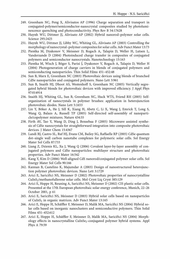
H. Hoppe · N.S. Sariciftci
249. Greenham NC, Peng X, Alivisatos AP (1996) Charge separation and transport inconjugated-polymer/semiconductor-nanocrystal composites studied by photolumi-nescence quenching and photoconductivity. Phys Rev B 54:17628
250. Huynh WU, Dittmer JJ, Alivisato AP (2002) Hybrid nanorod–polymer solar cells.Science 295:2425
251. Huynh WU, Dittmer JJ, Libby WC, Whiting GL, Alivisato AP (2003) Controlling themorphology of nanocrystal–polymer composites for solar cells. Adv Funct Mater 13:73
252. Pientka M, Dyakonov V, Meissner D, Rogach A, Talapin D, Weller H, Lutsen L,Vanderzande D (2004) Photoinduced charge transfer in composites of conjugatedpolymers and semiconductor nanocrystals. Nanotechnology 15:163
253. Pientka M, Wisch J, Böger S, Parisi J, Dyakonov V, Rogach A, Talapin D, Weller H(2004) Photogeneration of charge carriers in blends of conjugated polymers andsemiconducting nanoparticles. Thin Solid Films 451–452:48
254. Sun B, Marx E, Greenham NC (2003) Photovoltaic devices using blends of branchedCdSe nanoparticles and conjugated polymers. Nano Lett 3:961
255. Sun B, Snaith HJ, Dhoot AS, Westenhoff S, Greenham NC (2005) Vertically segre-gated hybrid blends for photovoltaic devices with improved efficiency. J Appl Phys97:014914
256. Snaith HJ, Whiting GL, Sun B, Greenham NC, Huck WTS, Friend RH (2005) Self-organization of nanocrystals in polymer brushes: application in heterojunctionphotovoltaic diodes. Nano Lett 5:1653
257. Lin Y, Böker A, He J, Sill K, Xiang H, Abetz C, Li X, Wang J, Emrick T, Long S,Wang Q, Balazs A, Russell TP (2005) Self-directed self-assembly of nanoparti-cle/copolymer mixtures. Nature 434:55
258. Firth AV, Tao Y, Wang D, Ding J, Bensebaa F (2005) Microwave assisted synthe-sis of CdSe nanocrystals for straightforward integration into composite photovoltaicdevices. J Mater Chem 15:4367
259. Landi BJ, Castro SL, Ruf HJ, Evans CM, Bailey SG, Raffaelle RP (2005) CdSe quantumdot–single wall carbon nanotube complexes for polymeric solar cells. Sol EnergyMater Sol Cells 87:733
260. Liang Z, Dzienis KL, Xu J, Wang Q (2006) Covalent layer-by-layer assembly of con-jugated polymers and CdSe nanoparticles: multilayer structure and photovoltaicproperties. Adv Funct Mater 16:542
261. Kang Y, Kim D (2006) Well-aligned CdS nanorod/conjugated polymer solar cells. SolEnergy Mater Sol Cells 90:166
262. Kannan B, Castelino K, Majumdar A (2003) Design of nanostructured heterojunc-tion polymer photovoltaic devices. Nano Lett 3:1729
263. Arici E, Sariciftci NS, Meissner D (2002) Photovoltaic properties of nanocrystallineCuInS2/methanofullerene solar cells. Mol Cryst Liq Cryst 385:129
264. Arici E, Hoppe H, Reuning A, Sariciftci NS, Meissner D (2002) CIS plastic solar cells.Presented at the 17th European photovoltaic solar energy conference, Munich, 22–26October 2001, p 61
265. Arici E, Sariciftci NS, Meissner D (2003) Hybrid solar cells based on nanoparticlesof CuInS2 in organic matrices. Adv Funct Mater 13:165
266. Arici E, Hoppe H, Schäffler F, Meissner D, Malik MA, Sariciftci NS (2004) Hybrid so-lar cells based on inorganic nanoclusters and semiconductive polymers. Thin SolidFilms 451–452:612
267. Arici E, Hoppe H, Schäffler F, Meissner D, Malik MA, Sariciftci NS (2004) Morph-ology effects in nanocrystalline CuInSe2-conjugated polymer hybrid systems. ApplPhys A 79:59
Polymer Solar Cells
268. Kang Y, Park N-G, Kim D (2005) Hybrid solar cells with vertically aligned CdTenanorods and a conjugated polymer. Appl Phys Lett 86:113101
269. Watt AAR, Blake D, Warner JH, Thomson EA, Tavenner EL, Rubinsztein-Dunlop H,Meredith P (2005) Lead sulfide nanocrystal:conducting polymer solar cells. J Phys DAppl Phys 38:2006
270. Zhang S, Cyr PW, McDonald SA, Konstantatos G, Sargent EH (2005) Enhancedinfrared photovoltaic efficiency in PbS nanocrystal/semiconducting polymer com-posites: 600-fold increase in maximum power output via control of the ligandbarrier. Appl Phys Lett 87:233101
271. Cui D, Xu J, Zhu T, Paradee G, Ashok S, Gerhold M (2006) Harvest of near in-frared light in PbSe nanocrystal–polymer hybrid photovoltaic cells. Appl Phys Lett88:183111
272. Günes S, Neugebauer H, Sariciftci NS, Roither J, Kovalenko M, Pillwein G, Heiss W(2006) Hybrid solar cells using HgTe nanocrystals and nanoporous TiO2 electrodes.Adv Funct Mater 16:1095
273. Beek WJE, Wienk MM, Janssen RAJ (2004) Efficient hybrid solar cells from zincoxide nanoparticles and a conjugated polymer. Adv Mater 16:1009
274. Beek WJE, Slooff LH, Wienk MM, Kroon JM, Janssen RAJ (2005) Hybrid solar cellsusing a zinc oxide precursor and a conjugated polymer. Adv Funct Mater 15:1703
275. Beek WJE, Wienk MM, Kemerink M, Yang X, Janssen RAJ (2005) Hybrid zinc oxideconjugated polymer bulk heterojunction solar cells. J Phys Chem B 109:9505
276. Beek WJE, Wienk MM, Janssen RAJ (2005) Hybrid polymer solar cells based on zincoxide. J Mater Chem 15:2985
277. Beek WJE, Wienk MM, Janssen RAJ (2006) Hybrid solar cells from regioregularpolythiophene and ZnO nanoparticles. Adv Funct Mater 16:1112
278. Greene LE, Law M, Tan DH, Montano M, Goldberger J, Somorjai G, Yang P (2005)General route to vertical ZnO nanowire arrays using textured ZnO seeds. Nano Lett5:1231
279. Quist PAC, Slooff LH, Donker H, Kroon JM, Savanije TJ, Siebbeles LDA (2005)Formation and decay of charge carriers in hybrid MDMO-PPV:ZnO bulk heterojunc-tions produced from a ZnO precursor. Superlattices Microstruct 38:308
280. Olson DC, Piris J, Collins RT, Shaheen SE, Ginley DS (2006) Hybrid photovoltaicdevices of polymer and ZnO nanofiber composites. Thin Solid Films 496:26
281. Peiro AM, Ravirajan P, Govender K, Boyle DS, O’Brien P, Bradley DDC, Nelson J,Durrant JR (2006) Hybrid polymer/metal oxide solar cells based on ZnO columnarstructures. J Mater Chem 16:2088
282. Ravirajan P, Peiro AM, Nazeeruddin MK, Graetzel M, Bradley DDC, Durrant JR, Nel-son J (2006) Hybrid polymer/zinc oxide photovoltaic devices with vertically orientedZnO nanorods and an amphiphilic molecular interface layer. J Phys Chem B 110:7635
283. O’Regan B, Grätzel M (1991) A low cost, high-efficiency solar cell based on dye-sensitized colloidal TiO2 films. Nature 353:737
284. Grätzel M (2001) Photoelectrochemical cells. Nature 414:338285. Bach U, Lupo D, Comte P, Moser JE, Weissörtel F, Salbeck J, Spreitzer H, Grätzel M
(1998) Solid-state dye-sensitized mesoporous TiO2 solar cells with high photon-to-electron conversion efficiencies. Nature 395:583
286. Krüger J, Bach U, Grätzel M (2000) Modification of TiO2 heterojunctions with ben-zoic acid derivatives in hybrid molecular solid-state devices. Adv Mater 12:447
287. Krüger J, Plass R, Cevey L, Piccirelli M, Grätzel M, Bach U (2001) High efficiencysolid-state photovoltaic device due to inhibition of interface charge recombination.Appl Phys Lett 79:2085
H. Hoppe · N.S. Sariciftci
288. Krüger J, Plass R, Grätzel M, Matthieu H-J (2002) Improvement of the photovoltaicperformance of solid-state dye-sensitized device by silver complexation of the sen-sitizer cis-bis(4,4-dicarboxy-2,2-bipyridine)-bis(isothiocyanato)ruthenium(II). ApplPhys Lett 81:367
289. Kim Y-G, Walker J, Samuelson LA, Kumar J (2003) Efficient light harvesting poly-mers for nanocrystalline TiO2 photovoltaic cells. Nano Lett 3:523
290. Senadeera GKR, Nakamura K, Kitamura T, Wada Y, Yanagida S (2003) Fabrication ofhighly efficient polythiophene-sensitized metal oxide photovoltaic cells. Appl PhysLett 83:5470
291. Nogueira AF, Longo C, De Paoli M-A (2004) Polymers in dye sensitized solar cells:overview and perspectives. Coord Chem Rev 248:1455
292. Arango AC, Carter SA, Brock PJ (1999) Charge transfer in photovoltaics consistingof interpenetrating networks of conjugated polymer and TiO2 nanoparticles. ApplPhys Lett 74:1698
293. Arango AC, Johnson LR, Bliznyuk VN, Schlesinger Z, Carter SA, Hörhold H-H(2000) Efficient titanium oxide/conjugated polymer photovoltaics for solar energyconversion. Adv Mater 12:1689
294. Salafsky JS (1999) Exciton dissociation, charge transport, and recombination in ul-trathin, conjugated polymer–TiO2 nanocrystal intermixed composites. Phys Rev B59:10885
295. Breeze AJ, Schlesinger Z, Carter SA (2001) Charge transport in TiO2/MEH-PPV poly-mer photovoltaics. Phys Rev B 64:125205
296. Gebeyehu D, Brabec CJ, Padinger F, Fromherz T, Spiekermann S, Vlachopoulos N,Kienberger F, Schindler H, Sariciftci NS (2001) Solid state dye-sensitized TiO2 solarcells with poly(3-octylthiophene) as hole transport layer. Synth Met 121:1549
297. Kaneko M, Takayama K, Pandey SS, Takashima W, Endo T, Rikukawa M, Kaneto K(2001) Photovoltaic cell using high mobility poly(alkylthiophene)s and TiO2. SynthMet 121:1537
298. Fan Q, McQuillin B, Bradley DDC, Whitelegg S, Seddon AB (2001) A solid-state solarcell using sol–gel processed material and a polymer. Chem Phys Lett 347:325
299. Qiao Q, McLeskey JJT (2005) Water-soluble polythiophene/nanocrystalline TiO2 so-lar cells. Appl Phys Lett 86:153501
300. Coakley KM, Srinivasan BS, Ziebarth JM, Goh C, Liu Y, McGehee MD (2005)Enhanced hole mobility in regioregular polythiophene infiltrated in straightnanopores. Adv Funct Mater 15:1927
301. Bartholomew GP, Heeger AJ (2005) Infiltration of regioregular poly[2,2′-(3-hexyl-thiophene)] into random nanocrystalline TiO2 networks. Adv Funct Mater 15:677
302. Ravirajan R, Bradley DDC, Nelson J, Haque SA, Durrant JR, Smit HJP, Kroon JM(2005) Efficient charge collection in hybrid polymer/TiO2 solar cells usingpoly(ethylenedioxythiophene)/polystyrene sulphonate as hole collector. Appl PhysLett 86:143101
303. Oey CC, Djurisic AB, Wang H, Man KKY, Chan WK, Xie MH, Leung YH, Pandey A,Nunzi J-M, Chui PC (2006) Polymer–TiO2 solar cells: TiO2 interconnected networkfor improved cell performance. Nanotechnology 17:706
304. van Hal PA, Wienk MM, Kroon JM, Verhees WJH, Slooff LH, van Gennip WJH,Jonkheijm P, Janssen RAJ (2003) Photoinduced electron transfer and photovoltaicresponse of a MDMO-PPV:TiO2 bulk heterojunction. Adv Mater 15:118
305. Slooff LH, Kroon JM, Loos J, Koetse MM, Sweelssen J (2005) Influence of the relativehumidity on the performance of polymer/TiO2 photovoltaic cells. Adv Funct Mater15:689
Polymer Solar Cells
306. Feng W, Feng Y, Wu Z (2005) Ultrasonic-assisted synthesis of poly(3-hexylthio-phene)/TiO2 nanocomposite and its photovoltaic characteristics. Jpn J Appl Phys44:7494
307. Iijima S (1991) Helical microtubes of graphitic carbon. Nature 354:56308. de Heer WA, Châtelain A, Ugarte D (1995) A carbon nanotube field-emission elec-
tron source. Science 270:1179309. Romero DB, Carrard M, De Heer W, Zuppiroli L (1996) A carbon nanotube/organic
semiconducting polymer heterojunction. Adv Mater 8:899310. Curran SA, Ajayan PM, Blau WJ, Carroll DL, Coleman JN, Dalton AB, Davey AP,
Drury A, McCarthy B, Maier S, Strevens A (1998) A composite from poly(m-phenylenevinylene-co-2,5-dioctoxy-p-phenylenevinylene) and carbon nanotubes:a novel material for molecular optoelectronics. Adv Mater 10:1091
311. Ago H, Petritsch K, Shaffer MSP, Windle AH, Friend RH (1999) Composites of carbonnanotubes and conjugated polymers for photovoltaic devices. Adv Mater 11:1281
312. Ago H, Kugler T, Cacialli F, Salaneck WR, Shaffer MSP, Windle AH, Friend RH(1999) Work functions and surface functional groups of multiwall carbon nano-tubes. J Phys Chem B 103:8116
313. Ago H, Shaffer MSP, Ginger DS, Windle AH, Friend RH (2000) Electronic interac-tion between photoexcited poly(p-phenylene vinylene) and carbon nanotubes. PhysRev B 61:2286
314. Kymakis E, Amaratunga GAJ (2002) Single-wall carbon nanotube/polymer photo-voltaic devices. Appl Phys Lett 80:112
315. Kymakis E, Alexandrou I, Amaratunga GAJ (2003) High open-circuit voltage photo-voltaic devices from carbon-nanotube–polymer composites. J Appl Phys 93:1764
316. Bhattacharyya S, Kymakis E, Amaratunga GAJ (2004) Photovoltaic properties ofdye functionalized single-wall carbon nanotube/conjugated polymer devices. ChemMater 16:4819
317. Kymakis E, Amaratunga GAJ (2005) Carbon nanotubes as electron acceptors in poly-meric photovoltaics. Rev Adv Mater Sci 10:300
318. Kazaoui S, Minami N, Nalini B, Kim Y, Hara K (2005) Near-infrared photoconductiveand photovoltaic devices using single-wall carbon nanotubes in conductive polymerfilms. J Appl Phys 98:084314
319. Rahman GMA, Guldi DM, Cagnoli R, Mucci A, Schenetti L, Vaccari L, Prato M (2005)Combining single-wall carbon nanotubes and photoactive polymers for photocon-version. J Am Chem Soc 127:10051
320. Guldi DM, Rahman GMA, Prato M, Jux N, Qin S, Ford W (2005) Single-wall carbonnanotubes as integrative building blocks for solar-energy conversion. Angew ChemInt Ed 44:2015
321. Landi BJ, Raffaelle RP, Castro SL, Bailey SG (2005) Single-wall carbon nanotube-polymer solar cells. Prog Photovoltaics Res Appl 13:165
322. Itoh E, Suzuki I, Miyairi K (2005) Field emission from carbon-nanotube-dispersedconducting polymer thin film and its application to photovoltaic devices. Jpn J ApplPhys 44:636
323. Rud JA, Lovell LS, Senn JW, Qiao Q, McLeskey JJT (2005) Water soluble poly-mer/carbon nanotube bulk heterojunction solar cells. J Mater Sci 40:1455
324. Kimura T, Ago H, Tobita M, Ohshima S, Kyotani M, Yumura M (2002) Polymercomposites of carbon nanotubes aligned by a magnetic field. Adv Mater 14:1380
325. Cao J, Sun J-Z, Hong J, Li H-Y, Chen H-Z, Wang M (2004) Carbon nanotube/CdScore–shell nanowires prepared by a simple room-temperature chemical reductionmethod. Adv Mater 16:84
H. Hoppe · N.S. Sariciftci
326. Robel I, Bunker BA, Kamat PV (2005) Single-walled carbon nanotube–CdS nano-composites as light-harvesting assemblies: photoinduced charge-transfer interac-tion. Adv Mater 17:2458
327. Pradhan B, Batabyal SK, Pal AJ (2006) Functionalized carbon nanotubes indonor/acceptor-type photovoltaic devices. Appl Phys Lett 88:093106
328. Patyk RL, Lomba BS, Nogueira AF, Furtado CA, Santos AP, Mello RMQ, Micaroni L,Hümmelgen IA (2007) Carbon nanotube–polybithiophene photovoltaic devices withhigh open-circuit voltage. Phys Status Solidi RRL 1:43
329. Xu Z, Wu Y, Hu B, Ivanov IN, Geohegan DB (2005) Carbon nanotube effects on elec-troluminescence and photovoltaic response in conjugated polymers. Appl Phys Lett87:263118
330. Pasquier AD, Unalan HE, Kanwal A, Miller S, Chhowalla M (2005) Conductingand transparent single-wall carbon nanotube electrodes for polymer–fullerene solarcells. Appl Phys Lett 87:203511
331. Ulbricht R, Jiang X, Lee S, Inoue K, Zhang M, Fang S, Baughman R, Zakhidov A(2006) Polymeric solar cell with oriented and strong transparent carbon nanotubeanode. Phys Status Solidi B 243:3528
332. van de Lagemaat J, Barnes TM, Rumbles G, Shaheen SE, Coutts TJ, Weeks C, Lev-itsky I, Peltola J, Glatkowski P (2006) Organic solar cells with carbon nanotubesreplacing In2O3:Sn as the transparent electrode. Appl Phys Lett 88:233503
333. Rowell MW, Topinka MA, McGehee MD, Prall H-J, Dennler G, Sariciftci NS, Hu L,Gruner G (2006) Organic solar cells with carbon nanotube network electrodes. ApplPhys Lett 88:233506