
14 2 2 - journal.esrgroups.org · Bab Ezzouar,Algiers, Algeria 2 Laboratory of Control Process,...
18
* Corresponding author: M. Ali, Faculty of Electronics and Computer, E-mail: [email protected] 1 Laboratory of Instrumentation, Faculty of Electronics and Computer, University of Sciences and Technology, Bab Ezzouar,Algiers, Algeria 2 Laboratory of Control Process, ENP, Algiers, Algeria ****** This paper is an extended version of a paper presented in International Conference on Recent Advances in Electrical Systems, ICRAES’17, Tunisia, 2017 Copyright © JES 2018 on-line : journal/esrgroups.org/jes Mounira Ali 1,* Abdelaziz Talha 1 , El Madjid Berkouk 2 J. Electrical Systems 14-2 (2018): 16-33 Regular paper A novel space vector pulse with modulation (SVPWM) algorithm with direct computation based on the neutral- point balancing problem in a three- level inverter analyzed using a redundant algorithm JES Journal of Journal of Journal of Journal of Electrical Electrical Electrical Electrical Systems Systems Systems Systems Owing to its high performances in terms of minimization of the harmonics and the switching losses as well as its ability to generate variable amplitude AC voltage for the same DC bus, the SVPWM is still widely used in the control of multi-level inverters. However, the requirement of the linear transformations and the large number of trigonometric functions is an important drawback of this algorithm, which increases its cost in terms of computation time. Consequently, the trade-off between the signal quality and the algorithm simplicity is still appears. In this way, a new technique is proposed to do this, an efficient SVPWM algorithm with feeble computational overhead based on voltage-second balance principle was needed, this technique for its simplicity on the one hand (simplify the calculation and reduce the computation time) on the one hand and on the other hand afford a contribution to the problem of neutral-point voltage balancing in three-level NPC converter in contrary conventional SVPWM algorithm who involves complex mathematics and requires more hardware resources to implement and takes more time for its execution. in this paper a novel space vector pulse with modulation (SVPWM) algorithm with direct computation based on the neutral-point balancing problem in a three- level inverter analyzed using a redundant algorithm is presented ,the proposed control strategies will be examined by simulation and real time implementation using Matlab/Simulink software with real time interface based on dSpace 1103 board ,the performance of the proposed control technique is demonstrated through simulation and experimental investigation. Keywords: Neutral point voltage; power; redundant algorithm; SVPWM; three level inverter. Article history: Received 21 December 2017, Accepted 14 April 2018 1. Introduction The Multilevel converters (MLCs) have recently been considered for medium- and high- voltage applications. The traditional solution to withstand high voltages involves connecting semiconductors in series; nonetheless, this solution requires rapid switching to avoid unequal voltage sharing among devices, and the process can induce a breakdown. MLCs can clamp voltages as an advantage, thus preventing the need for fast switching, and also generate a smoother output voltage than traditional two-level converters do. MLCs are suitable for application to wind turbines given their increasing power ratings. The neutral point-clamped (NPC) three-level converter is the most popular MLC and is the subject of the present research. A challenge of this converter is the high control complexity; considerable research has been conducted on the topology of this converter, and numerous control methods have been presented in literature. Recent studies focus on solving the
Transcript of 14 2 2 - journal.esrgroups.org · Bab Ezzouar,Algiers, Algeria 2 Laboratory of Control Process,...
* Corresponding author: M. Ali, Faculty of Electronics and Computer, E-mail: [email protected] 1Laboratory of Instrumentation, Faculty of Electronics and Computer, University of Sciences and Technology,
Bab Ezzouar,Algiers, Algeria 2
Laboratory of Control Process, ENP, Algiers, Algeria
****** This paper is an extended version of a paper presented in International Conference on Recent Advances in Electrical
Systems, ICRAES’17, Tunisia, 2017
Copyright © JES 2018 on-line : journal/esrgroups.org/jes
Mounira Ali1,*
Abdelaziz
Talha 1,
El Madjid
Berkouk2
J. Electrical Systems 14-2 (2018): 16-33
Regular paper
A novel space vector pulse with
modulation (SVPWM) algorithm with
direct computation based on the neutral-
point balancing problem in a three- level
inverter analyzed using a redundant
algorithm
JES
Journal of Journal of Journal of Journal of Electrical Electrical Electrical Electrical SystemsSystemsSystemsSystems
Owing to its high performances in terms of minimization of the harmonics and the switching losses as well as its ability to generate variable amplitude AC voltage for the same DC bus, the SVPWM is still widely used in the control of multi-level inverters. However, the requirement of the linear transformations and the large number of trigonometric functions is an important drawback of this algorithm, which increases its cost in terms of computation time. Consequently, the trade-off between the signal quality and the algorithm simplicity is still appears. In this way, a new technique is proposed to do this, an efficient SVPWM algorithm with feeble computational overhead based on voltage-second balance principle was needed, this technique for its simplicity on the one hand (simplify the calculation and reduce the computation time) on the one hand and on the other hand afford a contribution to the problem of neutral-point voltage balancing in three-level NPC converter in contrary conventional SVPWM algorithm who involves complex mathematics and requires more hardware resources to implement and takes more time for its execution. in this paper a novel space vector pulse with modulation (SVPWM) algorithm with direct computation based on the neutral-point balancing problem in a three- level inverter analyzed using a redundant algorithm is presented ,the proposed control strategies will be examined by simulation and real time implementation using Matlab/Simulink software with real time interface based on dSpace 1103 board ,the performance of the proposed control technique is demonstrated through simulation and experimental investigation.
Keywords: Neutral point voltage; power; redundant algorithm; SVPWM; three level inverter.
Article history: Received 21 December 2017, Accepted 14 April 2018
1. Introduction
The Multilevel converters (MLCs) have recently been considered for medium- and high-
voltage applications. The traditional solution to withstand high voltages involves
connecting semiconductors in series; nonetheless, this solution requires rapid switching to
avoid unequal voltage sharing among devices, and the process can induce a breakdown.
MLCs can clamp voltages as an advantage, thus preventing the need for fast switching, and
also generate a smoother output voltage than traditional two-level converters do. MLCs are
suitable for application to wind turbines given their increasing power ratings. The neutral
point-clamped (NPC) three-level converter is the most popular MLC and is the subject of
the present research. A challenge of this converter is the high control complexity;
considerable research has been conducted on the topology of this converter, and numerous
control methods have been presented in literature. Recent studies focus on solving the
J. Electrical Systems 14-2 (2018): 16-33
17
voltage fluctuation between two capacitors, and most works aimed to improve the direct
current (DC)–bus balance to address the imbalance in the continuous sources of multilevel
inverters. A few methods are based on the addition of sequences to zero voltage or on
continuous offsets at the output vector [1- 2] The method applied by [3,4] incorporates
power electronic circuits into an inverter to redistribute electrical charges. An approach was
also proposed in [5] based on the minimization of a quadratic function depending on the
voltages across capacitors. This quadratic function is positive definite and reaches zero
when the voltages across various capacitors are equal. Other techniques apply the theories
of automatic control by fuzzy logic, by neural networks, and by sliding mode [8-9-10-11-
12-13-14]. Different methods exhibit various disadvantages, such as high manufacturing
cost, installation complexity, or the implementation of settings in open loops only. The
utilization of the space-vector pulse-width modulation algorithm automatically induces
voltage fluctuations in the middle point and augments the output of low-order harmonics.
As a result, switch Voltage stress increases. The fluctuating voltage in the midpoint of a
three-level inverter restricts the developments of this inverter significantly; thus, the
effective control of these fluctuations considerably enhances the applicability of three-level
inverters. The current study analyzes the fluctuations in the middle-point potential of a
three-level inverter and then proposes action-time correction methods for basic voltage
vectors and for the original fundamental voltage vector.
2. Modeling of Three Level Inverter
Inverters are static converters which convert electrical power from a continuous form
into an alternating power. The output voltage of an inverter has a periodic waveform which
is not sinusoidal but can be very close to the desired waveform with a desired frequency.
The DC / AC converter presented above consists of three switching circuits which are
supplied by a direct current source. This voltage is obtained from a diode rectifier or from a
photovoltaic generator.
Among all topologies, three-phase three-level neutral-point clamped (NPC) PWM inverter
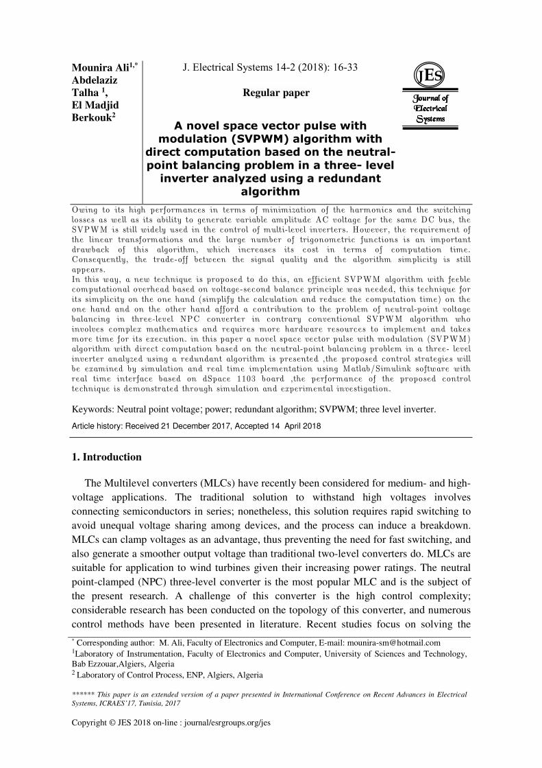
is the most widely used and investigated topology at present. Fig.1 presents the schematic
scheme of three-level NPC inverter. Each leg of the inverter consists of four power
switches (IGBT), four freewheeling diodes and two clamping diodes that limit the voltage
excursions across each device to half the input dc-bus voltage.
For three-level NPC inverter, each bridge leg has three different switching states. For
example, the switching state of phase A is shown in Table I.
Considering three-phase, the total switching states consist of 33=27 different states.
According to the magnitude value, these 27 switching states of the three level inverter
indicating each state with the combination of P, N and O states are classified by four
voltage vectors: one zero vector , six small vector whose length is / 3d cV , six middle vector
whose length is 3 / 3d cV , and six large vector whose length is 2 / 3d cV , as shown in Fig.2.
M. Ali et al: A novel space vector pulse with modulation (SVPWM) algorithm...
18
I2 2
C2
o
C1
v0
us1
i1
I3
1
3
Load I2 2
C2
o
C1
v0
us1
i1
I3
1
3
Load
I2 2
i1
I3
1
3
load
C2
o
C1
v0
us1
Im2
)(14 NNNv
r im2=0 )(7 PPPvr im2=0 )(0 OOOv
r im2=0
T23
T33
T43
T13
T22
T32
T42
T12
T21
T31
T41
T11
um1 iL1 RL
us1
C1
RL
RL um2
iL2 n
1
2
3
C2
vc1
vc1
Il3
p
N
im1
Im2 o
idc
Figure 1. Diagram of three-stage DC / AC converter
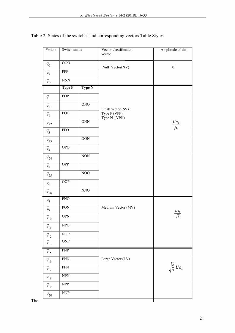
The zero vectors have three switching states (PPP, OOO, NNN). Each of the six small
vectors has two switching states and each of the middle Vectors and the large vectors has
one state respectively.
Table 1: Switching states of three-level inverter
Table.1 defines the states of the switch T11 of the first phase. The states of the switch are
defined as follows:
� Positive (P) when both top switches are closed
� Zero (O) when the two middle switches are closed
� Negative (N) when both bottom switches are closed
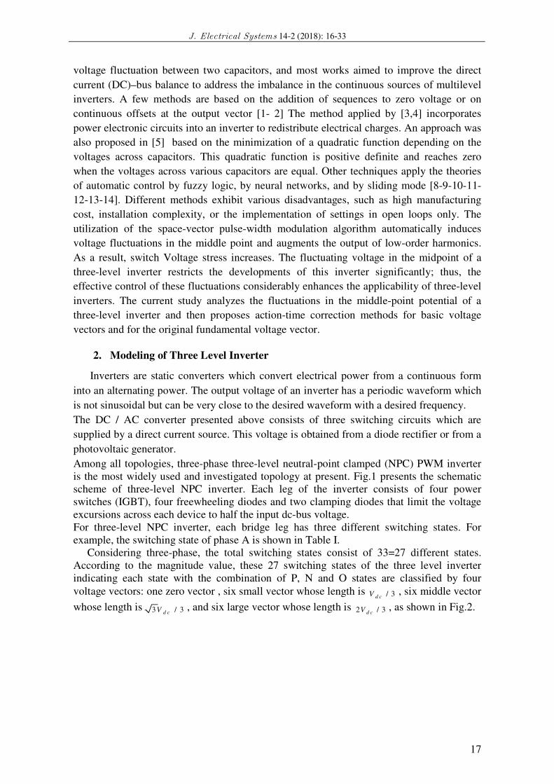
The null voltage vectors (VTN) generate zero modulated voltages and are obtained from
three different combinations of switch states: 0v (OOO),
7v (PPP) and 14v (NNN). These
vectors have no influence on the voltage of the midpoint of the converter. This is illustrated
in Figure 2 which shows the equivalent diagram with ideal switches of the converter
feeding a load for each of the three configurations representing the three null vectors.
The small hexagon (Figure 6.c) has twelve vectors. These vectors have an effect on the
voltage of the midpoint "O" because their application connects one or two currents from
the load at the midpoint. Indeed, six vectors among
Figure 2. Equivalent ideal converter for null vectors
state Output leg voltage Switch Sequence
VT1 VT2 VT3 VT4
P E ON ON OFF OFF
O 0 OFF ON ON OFF
N -E OFF OFF ON ON
J. Electrical Systems 14-2 (2018): 16-33
19
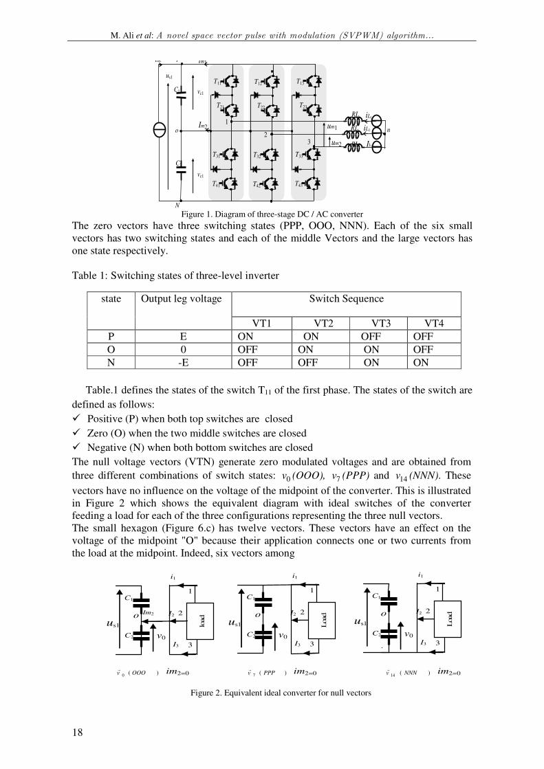
Them make it possible to charge the capacitor of the top C1, while the other six
discharge it Figure 3 presents the two configurations corresponding to the vectors 1vr
(POP)
and 21vr
(ONO) which make it possible to obtain the voltage / 2.
The small hexagon (Figure.9.c) has twelve vectors. These vectors have an effect on the
voltage of the midpoint "O" because their application connects one or two currents from
the load at the midpoint. Indeed, six vectors among them make it possible to charge the
capacitor of the top C1, while the other six discharge it. Figure 3 presents the two
configurations corresponding to the vectors 1vr
(POP) and 21vr
(ONO) which make it
possible to obtain the voltage / 2
Figure 3. Equivalent ideal converter for small vectors
Figure 3.1 shows that when the vector 1vr
(POP) is applied, the current of the neutral point
im2 is negative if the current i1 is positive (im2 = -i1 < 0). This causes the discharge of the
capacitor C1 and, consequently, the charge of the capacitor C2. On the other hand, when
the Vector 21vr
(ONO) (Figure 3.2) is applied, the current of the neutral point im2 is positive
if the current i1 is positive (im2 = i1> 0) which leads to the charging of the capacitor C1
and the discharge of the capacitor C2.
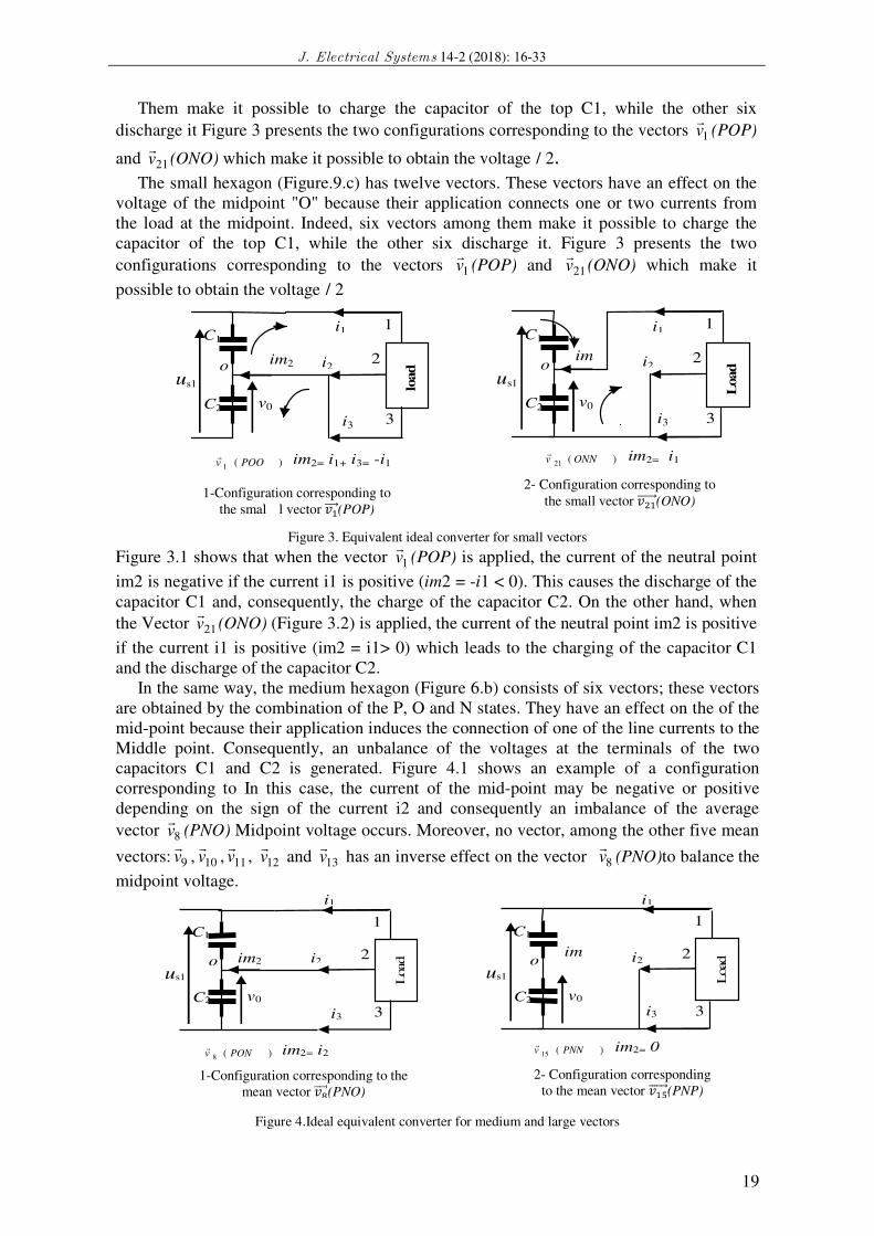
In the same way, the medium hexagon (Figure 6.b) consists of six vectors; these vectors
are obtained by the combination of the P, O and N states. They have an effect on the of the
mid-point because their application induces the connection of one of the line currents to the
Middle point. Consequently, an unbalance of the voltages at the terminals of the two
capacitors C1 and C2 is generated. Figure 4.1 shows an example of a configuration
corresponding to In this case, the current of the mid-point may be negative or positive
depending on the sign of the current i2 and consequently an imbalance of the average
vector 8vr
(PNO) Midpoint voltage occurs. Moreover, no vector, among the other five mean
vectors: 9vr
, 10vr
, 11vr
,
12vr
and 13vr
has an inverse effect on the vector 8vr
(PNO)to balance the
midpoint voltage.
Figure 4.Ideal equivalent converter for medium and large vectors
C2
o
C1
v0
us1
i1
i3
1
3
L
oad
)(21 ONNvr im2= i1
)(1 POOvr im2= i1+ i3= -i1
i2 2 im
C2
o
C1
v0
us1
3 load i2 2 im2
1 i1
i3
1-Configuration corresponding to
the smal l vector ������(POP)
2- Configuration corresponding to
the small vector ����������(ONO)
C2
o
C1
v0
us1
i1
i3
1
3
Load
)(15 PNNvr im2= 0
)(8 PONvr im2= i2
i2 2 im
C2
o
C1
v0
us1
3
Load i2 2 im2
1
i1
i3
2- Configuration corresponding
to the mean vector ����������(PNP) 1-Configuration corresponding to the
mean vector �������(PNO)
M. Ali et al: A novel space vector pulse with modulation (SVPWM) algorithm...
20
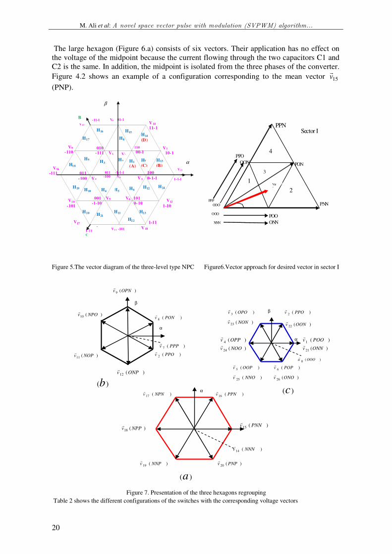
The large hexagon (Figure 6.a) consists of six vectors. Their application has no effect on
the voltage of the midpoint because the current flowing through the two capacitors C1 and
C2 is the same. In addition, the midpoint is isolated from the three phases of the converter.
Figure 4.2 shows an example of a configuration corresponding to the mean vector 15vr
(PNP).
Figure 5.The vector diagram of the three-level type NPC Figure6.Vector approach for desired vector in sector I
Figure 7. Presentation of the three hexagons regrouping
Table 2 shows the different configurations of the switches with the corresponding voltage vectors
100
V1 0-1-1
011 -1-1-1
-100 V0
011
-100 V4
V8 01-1
1-11
V 18
V17
H23
H22
H21
H20 H11
V1 1 -101
β
-11-1
V1 5 V 14
11-1
-
1-11 C
B
A
H17
H16 H15 H14
(D) H8
V2
H5
010
-111 V3
110
00-1
V7
10-1
V9
-110
V13
1-1-1
V16
-111
α H18
H13
(B)
H9 H7
(C) H3
H2 H1
(A)
V6 101
0-10
001 V5 -1-10
V12
1-10
V10
-101
H24 H19 H12 H10 H6 H4
)(c
)(a
)(b
)(24 NOOvr
)(5 OOPvr )(6 POPv
r
)(0
OOOur
)(25 NNOvr )(26 ONOv
r
)(4 OPPvr
)(21 ONNvr
)(1 POOvr
)(2 PPOvr
)(22 OONvr
)(3 OPOvr
)(23 NONvr
)(18 NPPvr
)(14 NNNvr
)(19 NNPvr )(20 PNPv
r
)(15 PNNvr
)(16 PPNvr )(17 NPNv
r
α
)(7 PPPvr
)(9 OPNvr
)(12 ONPvr
)(2 PPOvr )(11 NOPv
r
)(8 PONvr )(10 NPOv
r β
α
α
β
Sector I
PPP
OOO
OOO
NNN
PPO
OON
POO
ONN
PPN
PNN
PON
Vre
f
4
3
2
1
J. Electrical Systems 14-2 (2018): 16-33
21
Table 2: States of the switches and corresponding vectors Table Styles
The
Vectors Switch status Vector classification Amplitude of the
vector
0vr
OOO
Null Vector(NV) 0
7vr
PPP
14vr
NNN
Type P Type N
Small vector (SV) :
Type P (VPP)
Type N (VPN)
�√
1vr
POP
21vr
ONO
2vr
POO
22vr
ONN
3vr
PPO
23vr
OON
4vr
OPO
24vr
NON
5vr
OPP
25vr
NOO
6vr
OOP
26vr
NNO
8vr
PNO
Medium Vector (MV)
�√�
9vr
PON
10vr
OPN
11vr
NPO
12vr
NOP
13vr
ONP
15vr
PNP
Large Vector (LV) ��
� ���
16vr
PNN
17vr
PPN
18vr
NPN
19vr
NPP
20vr
NNP
M. Ali et al: A novel space vector pulse with modulation (SVPWM) algorithm...
22
space vector diagram is divided into six triangle sections by six large voltage vectors. If we
start from the large voltage vector PNN, the whole region can be defined as sectors I, II…
and VI every 60 degrees. And each sector is divided into four sub triangles as shown in
Figure 7. Sector I is usually analyzed firstly. Then the result of the whole 360 degree region
can be achieved according to its symmetry characteristic.
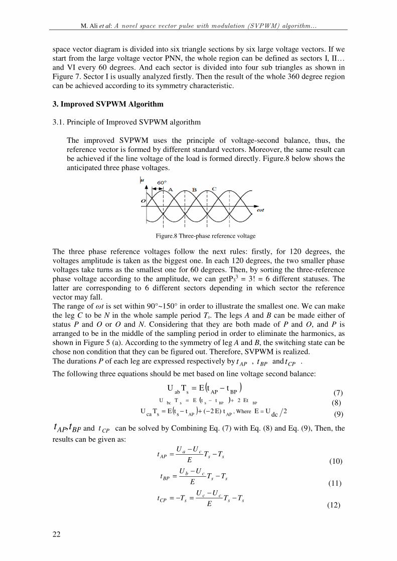
3. Improved SVPWM Algorithm
3.1. Principle of Improved SVPWM algorithm
The improved SVPWM uses the principle of voltage-second balance, thus, the
reference vector is formed by different standard vectors. Moreover, the same result can
be achieved if the line voltage of the load is formed directly. Figure.8 below shows the
anticipated three phase voltages.
Figure.8 Three-phase reference voltage
The three phase reference voltages follow the next rules: firstly, for 120 degrees, the
voltages amplitude is taken as the biggest one. In each 120 degrees, the two smaller phase
voltages take turns as the smallest one for 60 degrees. Then, by sorting the three-reference
phase voltage according to the amplitude, we can getP33 = 3! = 6 different statuses. The
latter are corresponding to 6 different sectors depending in which sector the reference
vector may fall.
The range of ωt is set within 90°~150° in order to illustrate the smallest one. We can make
the leg C to be N in the whole sample period Ts. The legs A and B can be made either of
status P and O or O and N. Considering that they are both made of P and O, and P is
arranged to be in the middle of the sampling period in order to eliminate the harmonics, as
shown in Figure 5 (a). According to the symmetry of leg A and B, the switching state can be
chose non condition that they can be figured out. Therefore, SVPWM is realized.
The durations P of each leg are expressed respectively by APt , BPt and CPt .
The following three equations should be met based on line voltage second balance:
( )
BPAPsabttETU −=
(7)
( )BPBP
Et2ttETUssbc
+−= (8)
( ) 2dc
UEtE)2(ttETU Where,ssca APAP
=−+−=
(9)
BPAP t,t and CPt can be solved by Combining Eq. (7) with Eq. (8) and Eq. (9), Then, the
results can be given as:
ss
caAP TT
E
UUt −
−=
(10)
ss
cbBP TT
E
UUt −
−=
(11)
ss
ccsCP TT
E
UUTt −
−=−=
(12)
J. Electrical Systems 14-2 (2018): 16-33
23
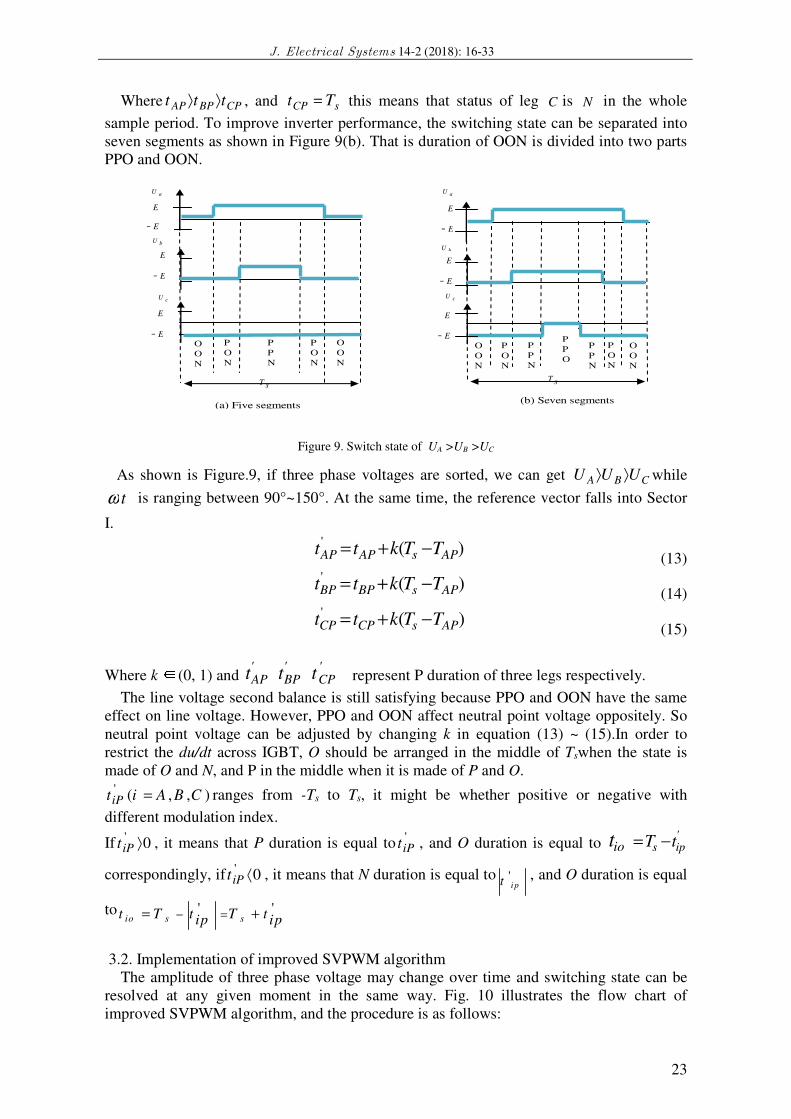
Where CPBPAP ttt ⟩⟩ , and sCP Tt = this means that status of leg C is N in the whole
sample period. To improve inverter performance, the switching state can be separated into
seven segments as shown in Figure 9(b). That is duration of OON is divided into two parts
PPO and OON.
Figure 9. Switch state of UA >UB >UC
As shown is Figure.9, if three phase voltages are sorted, we can get CBA UUU ⟩⟩ while
tω is ranging between 90°~150°. At the same time, the reference vector falls into Sector
I.
)('APsAPAP TTktt −+=
(13)
)('APsBPBP TTktt −+=
(14)
)('APsCPCP TTktt −+=
(15)
Where k ∈ (0, 1) and 'APt
'BPt
'CPt represent P duration of three legs respectively.
The line voltage second balance is still satisfying because PPO and OON have the same
effect on line voltage. However, PPO and OON affect neutral point voltage oppositely. So
neutral point voltage can be adjusted by changing k in equation (13) ~ (15).In order to
restrict the du/dt across IGBT, O should be arranged in the middle of Tswhen the state is
made of O and N, and P in the middle when it is made of P and O. '
( , , )iPt i A B C= ranges from -Ts to Ts, it might be whether positive or negative with
different modulation index.
If '0iPt ⟩ , it means that P duration is equal to '
iPt , and O duration is equal to 'ips tTiot −=
correspondingly, if ' 0iPt ⟨ , it means that N duration is equal to 'i pt , and O duration is equal
to ' 'io s st T t T tip ip=−= +
3.2. Implementation of improved SVPWM algorithm
The amplitude of three phase voltage may change over time and switching state can be
resolved at any given moment in the same way. Fig. 10 illustrates the flow chart of
improved SVPWM algorithm, and the procedure is as follows:
cU
bU
aU
- E
E
- E
E
- E
E
O
O
N
P
O
N
P
P
N
P
P
N
O
O
N
P
O
N
P
P
O
sT
(b) Seven segments
O
O
N
P
O
N
P
P
N
P
O
N
O
O
N
(a) Five segments
cU
bU
- E
E
- E
E
sT
aU
- E
E
M. Ali et al: A novel space vector pulse with modulation (SVPWM) algorithm...
24
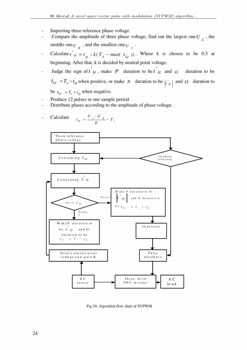
- Importing three reference phase voltage.
- Compare the amplitude of three phase voltage, find out the largest oneL
U , the
middle oneM
U , and the smallest oneS
U .
- Calculate ))itmax(T(kt'tpSip
ip −= + . Where k is chosen to be 0.5 at
beginning. After that, k is decided by neutral point voltage.
- Judge the sign of ip't , make P duration to be ip
't and O duration to be
'ips tTiot −= when positive, or make N duration to be
ipt ' and O duration to
be 'ips tTiot += when negative.
- Produce 12 pulses in one sample period.
- Distribute pluses according to the amplitude of phase voltage.
- Calculate sT
E
sUU
t iip −=
−
N é g a ti ve
P o s i ti v
e
C a lc u l a t i n g ip't
M a k e P d u r a t io n to
b e ip't a n d O
d u r a t io n to b e 'ips tTi ot −=
T h e re ré fé r e n c e
p h a s e v o l ta g e
C a lc u la t in g ipt
D e te c t n e u t ra l p o in t
v o l ta g e a n d a j u s t K
D C
s o u r c e
T h r e e - l e v e l
N P C in v e rte r A C
lo a d
P u ls e
d is t rib u t o
r
Im p u l s a t o r
M a k e N d u r a t i o n t o b e
ip't a n d O d u ra t i o n t o
b e 'ips tTi ot +=
S ig n o f ipt '
A m p lit u d e
co m p a ri n g
Fig.10. Algorithm flow chart of SVPWM
J. Electrical Systems 14-2 (2018): 16-33
25
3.3 Problem of Neutral point voltage imbalance
The main reasons why the capacitors are unbalance dare caused by the disagreement of
the switches parameters. In addition, the structure of three level converter itself. Both
reasons are impersonal existence and can solved only by control algorithm.
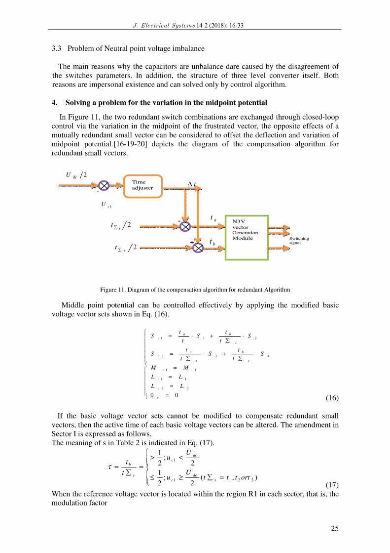
4. Solving a problem for the variation in the midpoint potential
In Figure 11, the two redundant switch combinations are exchanged through closed-loop
control via the variation in the midpoint of the frustrated vector, the opposite effects of a
mutually redundant small vector can be considered to offset the deflection and variation of
midpoint potential.[16-19-20] depicts the diagram of the compensation algorithm for
redundant small vectors.
Figure 11. Diagram of the compensation algorithm for redundant Algorithm
Middle point potential can be controlled effectively by applying the modified basic
voltage vector sets shown in Eq. (16).
=
=
=
=
⋅∑
+⋅∑
=
⋅∑
+⋅=
00
22
11
11
432
211
c
c
c
c
s
b
s
a
c
s
ba
c
LL
LL
MM
St
tS
t
tS
St
tS
t
tS
(16)
If the basic voltage vector sets cannot be modified to compensate redundant small
vectors, then the active time of each basic voltage vectors can be altered. The amendment in
Sector I is expressed as follows.
The meaning of s in Table 2 is indicated in Eq. (17).
=∑≥≤
<>
=∑
=
),(2
;2
1
2;
2
1
3211
1
orttttU
u
Uu
t
t
s
dc
c
dc
c
s
bτ
(17)
When the reference voltage vector is located within the region R1 in each sector, that is, the
modulation factor
N3V
vector Generation
Module Switching
signal
2s
t ∑
2s
t ∑
Time
adjuster
at
bt
-
+
2dcU
1cU
- t∆
M. Ali et al: A novel space vector pulse with modulation (SVPWM) algorithm...
26
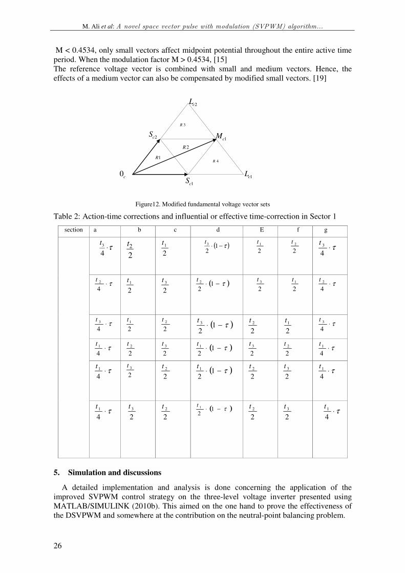
M < 0.4534, only small vectors affect midpoint potential throughout the entire active time
period. When the modulation factor M > 0.4534, [15]
The reference voltage vector is combined with small and medium vectors. Hence, the
effects of a medium vector can also be compensated by modified small vectors. [19]
Figure12. Modified fundamental voltage vector sets
Table 2: Action-time corrections and influential or effective time-correction in Sector 1
5. Simulation and discussions
A detailed implementation and analysis is done concerning the application of the
improved SVPWM control strategy on the three-level voltage inverter presented using
MATLAB/SIMULINK (2010b). This aimed on the one hand to prove the effectiveness of
the DSVPWM and somewhere at the contribution on the neutral-point balancing problem.
section a b c d E f g
τ⋅
4
3t
2
2t
2
1t
( )τ−⋅ 12
3t
2
1t
2
2t
τ⋅4
3t
τ⋅4
2t
2
1t
2
3t
( )τ−⋅ 12
2t
2
3t
2
1t
τ⋅4
2t
τ⋅4
3t
2
1t
2
2t
( )τ−⋅ 1
2
3t
2
2t
2
1t
τ⋅4
3t
τ⋅4
1t
2
2t
2
3t
( )τ−⋅ 1
2
1t
2
3t
2
2t
τ⋅
4
1t
τ⋅4
1t
2
3t
2
2t
( )τ−⋅ 12
1t
2
2t
2
3t
τ⋅4
1t
τ⋅4
1t
2
3t
2
2t
( )τ−⋅ 12
1t
2
2t
2
3t
τ⋅4
1t
1R
2R
3R
2cL
2cS 1cM
4R
1cL c0
1cS
J. Electrical Systems 14-2 (2018): 16-33
27
-500 -400 -300 -200 -100 0 100 200 300 400 500-400
-300
-200
-100
0
100
200
300
400
V0
V5
V23
V3
V4
V22
V19
V20
V21 V1
V6
V24
V2
V18
V15
V26
V25
V16
V17
0 0.005 0.01 0.015 0.02 0.025 0.03 0.035 0.041
1.5
2
2.5
3
3.5
4
4.5
5
5.5
6
T(s)
Sector
0 0.005 0.01 0.015 0.02 0.025 0.03 0.035 0.04-1
0
1
2
3
4
5x 10
-4
T(s)
t'iP
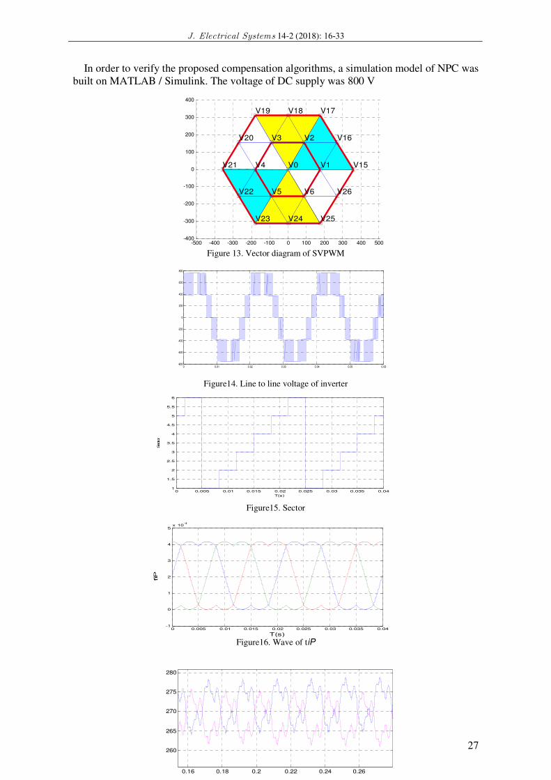
In order to verify the proposed compensation algorithms, a simulation model of NPC was
built on MATLAB / Simulink. The voltage of DC supply was 800 V
Figure 13. Vector diagram of SVPWM
Figure14. Line to line voltage of inverter
Figure15. Sector
Figure16. Wave of tiP
0 0.01 0.02 0.03 0.04 0.05 0.06-800
-600
-400
-200
0
200
400
600
800
0.16 0.18 0.2 0.22 0.24 0.26
260
265
270
275
280
M. Ali et al: A novel space vector pulse with modulation (SVPWM) algorithm...
28
0 0.05 0.1 0.15 0.2 0.25 0.3 0.35 0.4200
250
300
350
400
450
500
550
600
0 0.05 0.1 0.15 0.2 0.25 0.3 0.35 0.4200
250
300
350
400
450
500
550
600
0 0.05 0.1 0.15 0.2 0.25 0.3 0.35 0.4100
150
200
250
300
350
400
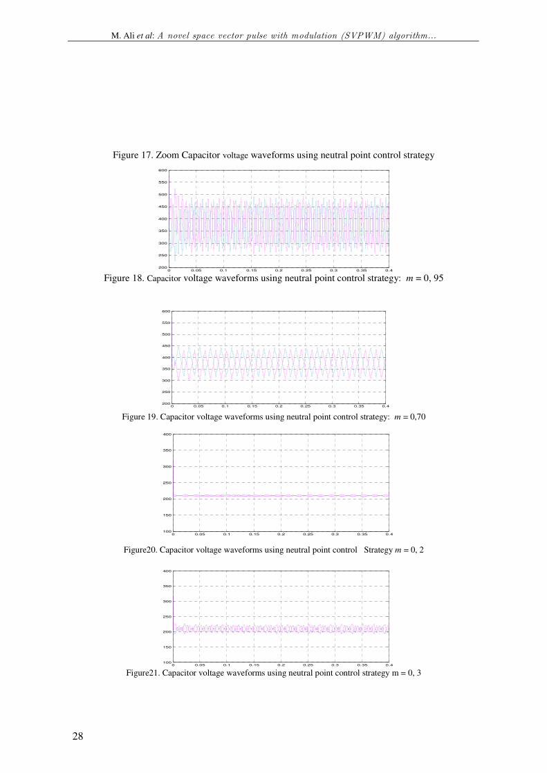
Figure 17. Zoom Capacitor voltage waveforms using neutral point control strategy
Figure 18. Capacitor voltage waveforms using neutral point control strategy: m = 0, 95
Figure 19. Capacitor voltage waveforms using neutral point control strategy: m = 0,70
Figure20. Capacitor voltage waveforms using neutral point control Strategy m = 0, 2
Figure21. Capacitor voltage waveforms using neutral point control strategy m = 0, 3
0 0.05 0.1 0.15 0.2 0.25 0.3 0.35 0.4100
150
200
250
300
350
400
J. Electrical Systems 14-2 (2018): 16-33
29
0 0.05 0.1 0.15 0.2 0.25 0.3 0.35 0.4100
150
200
250
300
350
400
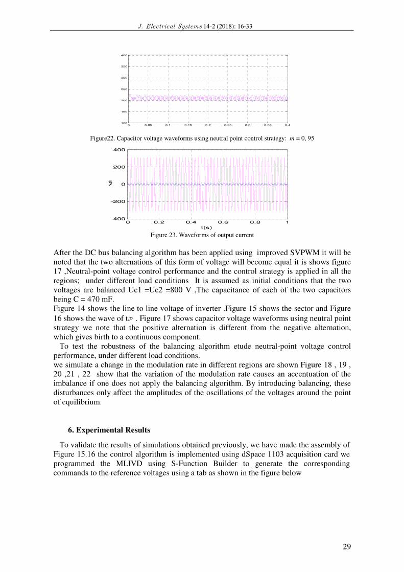
Figure22. Capacitor voltage waveforms using neutral point control strategy: m = 0, 95
Figure 23. Waveforms of output current
After the DC bus balancing algorithm has been applied using improved SVPWM it will be
noted that the two alternations of this form of voltage will become equal it is shows figure
17 ,Neutral-point voltage control performance and the control strategy is applied in all the
regions; under different load conditions It is assumed as initial conditions that the two
voltages are balanced Uc1 =Uc2 =800 V ,The capacitance of each of the two capacitors
being C = 470 mF.
Figure 14 shows the line to line voltage of inverter .Figure 15 shows the sector and Figure
16 shows the wave of tiP . Figure 17 shows capacitor voltage waveforms using neutral point
strategy we note that the positive alternation is different from the negative alternation,
which gives birth to a continuous component.
To test the robustness of the balancing algorithm etude neutral-point voltage control
performance, under different load conditions.
we simulate a change in the modulation rate in different regions are shown Figure 18 , 19 ,
20 ,21 , 22 show that the variation of the modulation rate causes an accentuation of the
imbalance if one does not apply the balancing algorithm. By introducing balancing, these
disturbances only affect the amplitudes of the oscillations of the voltages around the point
of equilibrium.
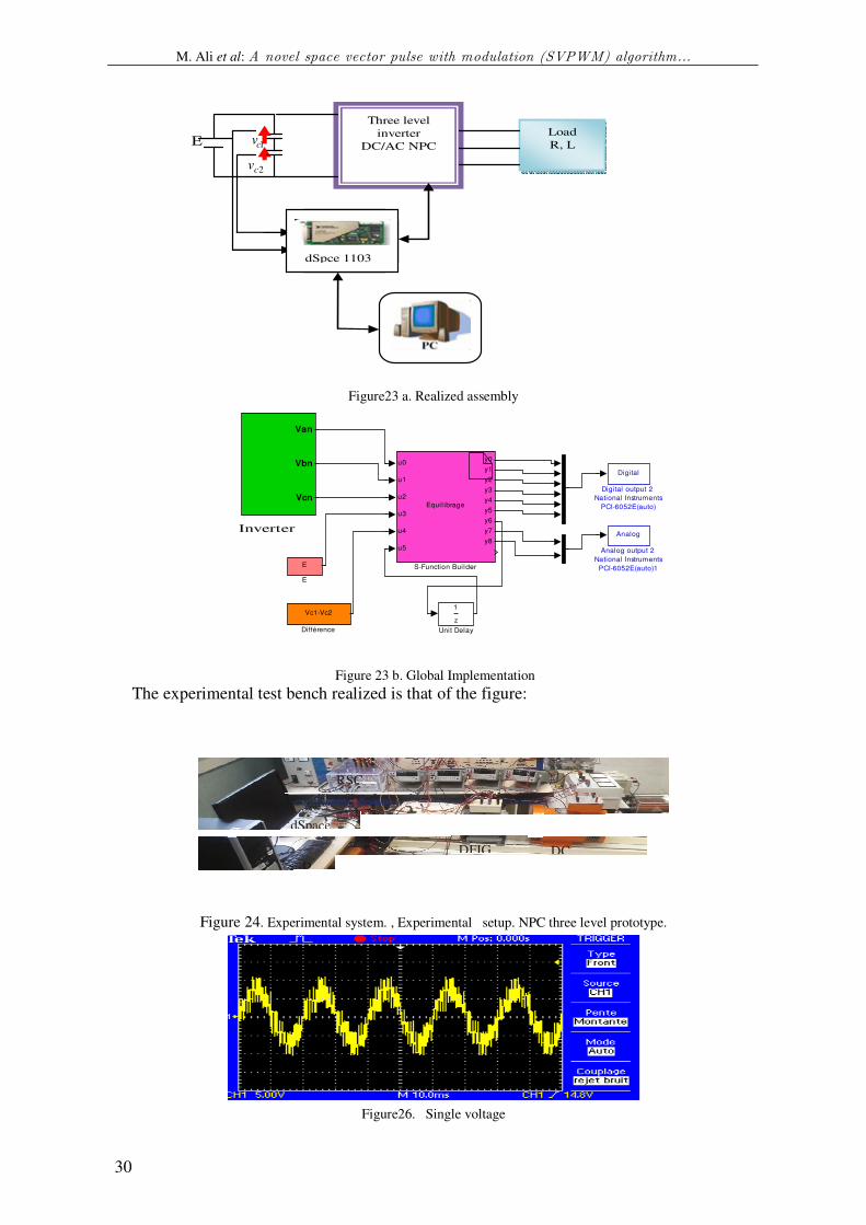
6. Experimental Results
To validate the results of simulations obtained previously, we have made the assembly of
Figure 15.16 the control algorithm is implemented using dSpace 1103 acquisition card we
programmed the MLIVD using S-Function Builder to generate the corresponding
commands to the reference voltages using a tab as shown in the figure below
0 0.2 0.4 0.6 0.8 1-400
-200
0
200
400
t(s)
V,I
M. Ali et al: A novel space vector pulse with modulation (SVPWM) algorithm...
30
Figure23 a. Realized assembly
Figure 23 b. Global Implementation
The experimental test bench realized is that of the figure:
Figure 24. Experimental system. , Experimental setup. NPC three level prototype.
Figure26. Single voltage
E
Three level
inverter
DC/AC NPC Load
R, L 1cv
2cv
dSpce 1103
z
1
Unit Delay
Equil ibrage
u0
u1
u2
u3
u4
u5
y0
y1
y2
y3
y4
y5
y6
y7
y8
S-Function Builder
Van
Vbn
Vcn
Onduleur
E
E
Digital
Digital output 2
National Instruments
PCI-6052E(auto)
Vc1-Vc2
Différence
Analog
Analog output 2
National Instruments
PCI-6052E(auto)1
Inverter
RSC
dSpace
DFIG DC P
J. Electrical Systems 14-2 (2018): 16-33
31
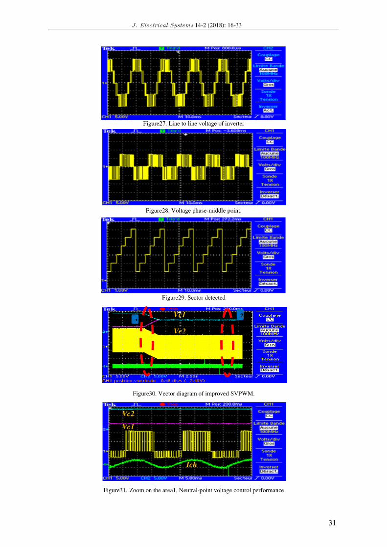
Figure27. Line to line voltage of inverter
Figure28. Voltage phase-middle point.
Figure29. Sector detected
Figure30. Vector diagram of improved SVPWM.
Figure31. Zoom on the area1, Neutral-point voltage control performance
1 2 Vc1
Vc2
Vc2
Vc1
Ich
M. Ali et al: A novel space vector pulse with modulation (SVPWM) algorithm...
32
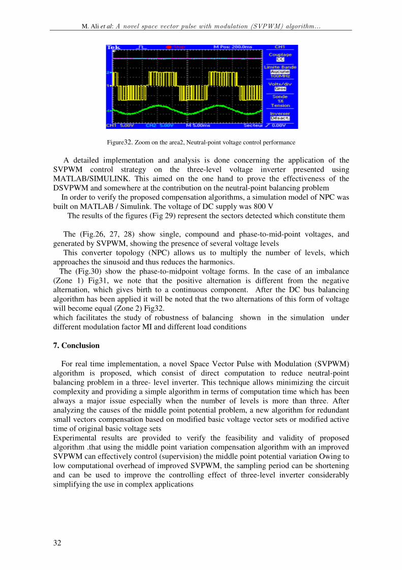
Figure32. Zoom on the area2, Neutral-point voltage control performance
A detailed implementation and analysis is done concerning the application of the
SVPWM control strategy on the three-level voltage inverter presented using
MATLAB/SIMULINK. This aimed on the one hand to prove the effectiveness of the
DSVPWM and somewhere at the contribution on the neutral-point balancing problem
In order to verify the proposed compensation algorithms, a simulation model of NPC was
built on MATLAB / Simulink. The voltage of DC supply was 800 V
The results of the figures (Fig 29) represent the sectors detected which constitute them
The (Fig.26, 27, 28) show single, compound and phase-to-mid-point voltages, and
generated by SVPWM, showing the presence of several voltage levels
This converter topology (NPC) allows us to multiply the number of levels, which
approaches the sinusoid and thus reduces the harmonics.
The (Fig.30) show the phase-to-midpoint voltage forms. In the case of an imbalance
(Zone 1) Fig31, we note that the positive alternation is different from the negative
alternation, which gives birth to a continuous component. After the DC bus balancing
algorithm has been applied it will be noted that the two alternations of this form of voltage
will become equal (Zone 2) Fig32.
which facilitates the study of robustness of balancing shown in the simulation under
different modulation factor MI and different load conditions
7. Conclusion
For real time implementation, a novel Space Vector Pulse with Modulation (SVPWM)
algorithm is proposed, which consist of direct computation to reduce neutral-point
balancing problem in a three- level inverter. This technique allows minimizing the circuit
complexity and providing a simple algorithm in terms of computation time which has been
always a major issue especially when the number of levels is more than three. After
analyzing the causes of the middle point potential problem, a new algorithm for redundant
small vectors compensation based on modified basic voltage vector sets or modified active
time of original basic voltage sets
Experimental results are provided to verify the feasibility and validity of proposed
algorithm .that using the middle point variation compensation algorithm with an improved
SVPWM can effectively control (supervision) the middle point potential variation Owing to
low computational overhead of improved SVPWM, the sampling period can be shortening
and can be used to improve the controlling effect of three-level inverter considerably
simplifying the use in complex applications
J. Electrical Systems 14-2 (2018): 16-33
33
References
[1] Gevork gharehpetian, Sanaz Namayan, Mehrdad abedi, Ali bidadfar, Novel control strategy for voltage
source converters based on energy function. Turk J Elec Eng & Comp Sci (2013) 21: 924 – 933.
[2] Akash S.Pabbewar M.Kowsalya Dr Three Level Neutral Point Clamped Inverter Using Space Vector
Modulation with Proportional Resonant Controller Energy Procedia Volume 103, December 2016, Pages
286-291. [3] Meng-jiang Tsai, Wei-lun Huang, Pei-yuan Chu, Hsin-chih Chen, Ping-heng Wu and Po-tai Cheng ,DC
Link Capacitor Voltage Balancing in Three Level Neutral point Clamped Inverter, Conference: 2016 IEEE
Energy Conversion Congress and Exposition (ECCE).
[4] Deng, Y.; Teo, K.H.; Harley, R.G. Generalized DC-link Voltage Balancing Control Method for Multilevel
Inverters, TR2013-005 March 2013.
[5] Zeliang Shu ; Xiaoqiong He ; Zhiyong Wang ; Daqiang Qiu ; Yongzi Jing ,Voltage Balancing
Approaches for Diode-Clamped Multilevel Converters Using Auxiliary Capacitor-Based Circuits, IEEE
Transactions on Power Electronics , Volume: 28, Issue: 5, May 2013 .
[6] Rédha. CHIBANI; ElMadjid. BERKOUK ; Mohamed Seghir BOUCHERIT ,Study of a new DC voltage
equalising circuit for Five-Level Neutral Point Clamped-Voltage Source Inverter, J. Electrical Systems 7-2 (2011): 131-148.
[7] K.Mohan Krishna ,J.N.ChandraSekhar ,Dr.G.V.Marutheswar , Modeling and Simulation of Three Level
VSI-Neutral Point Balancing -Fed AC Drive using Intelligence Techniques, Journal of Engineering Research and Applications, Vol. 5, Issue 12, December 2015, pp.174-182 .
[8] Mohammad Mardaneh, Faranak Golestaneh , Harmonic Optimization of Diode-clamped Multilevel Inverter
Using Teaching-learning-based Optimization Algorithm, Journal IETE Journal of Research Volume 59,
2013.
[9] Thameur abdelkrim, El madjid berkouk, Tarak benslimane, Karima benamrane, Feedback control of three-
Level PWM rectifier: Application to the stabilization of DC Voltages of five-level NPC active power filter, Archives of Control Sciences Volume 20(LVI), 2010 No. 3, pages 317–339
[10] Amirhossein Moeini , Shuo Wang, A DC Link Voltage Balancing Technique for Cascaded H-Bridge
Multilevel Converters with Asymmetric Selective Harmonic Current Mitigation-PWM, IEEE Transactions on Power Electronics,.2017.TPEL.2017.2770141.
[11] A. Narendrababu , Pramod Agarwal, Hybrid modulation strategy for elimination low-frequency NP voltage
oscillation in NPC using redistribution of NTV duty ratios Volume 10, Issue 12, 06 October 2017, p. 1504 –
1517 [12] E. M. B. A. Talha, F. Bouchafaa, M. S. Boucherit, "New algebraic PWM strategy of a seven – level NPC
voltage source inverter," AMSE, Rouen, France, 22 th – 24 th November – 2005. [13] E. M. B. H. Gheraia, G. Manesee, "Feedback Control of the Input dc Voltage Sources of the Seven Levels
NPC Voltage Source Inverter," Proceedings on IEEE AFRICON.99, pp. 691-696. [14] E. M. B. D. Beriber, A. Talha and M. O. Mahmoudi, "Study and control of two two - level pwm rectifiers -
clamping bridge - two three - level npc vsi cascade. Application to double stator induction machine," PESC
Record - IEEE Annual Power Electronics Specialists Conference, pp. 3894-3899, 2004. [15] s. c. bo gong, "Simple three-level neutral point voltage balance control strategy based on SVPWM " YI QIN
vol. 62, pp. 15-23, 2013 [16] R. l. n. mallikarjuna g. d, and suresh h. jangamshetti, "Space Vector Modulation Technique for Three Level
Diode Clamped Inverter " IJPE, vol. 4, 2012. [17] W.-g. Z. W. Y. R.-q. L. Bo Fan 1, "A Simplified SVPWM Algorithm Research Based on the Neutral-Point
Voltage Balance for NPC Three-level Inverter " Proceeding of the IEEE International Conference on
Automation and Logistics Zhengzhou, China, August 2012. [18] C. W. Bo Guan, "A Narrow Pulse Compensation Method for Neutral-Point-Clamped Three-Level
Converters Considering Neutral-Point Balance " 9th International Conference on Power Electronics-ECCE
Asia June 1 - 5, 2015 / 63 Convention Center, Seoul, Korea, 2015. [19] Masaoud A, Ping WH, Mekhilef S, Belkamel H. Highly efficient three-phase three-level multilevel inverter
employing different commutation strategies. Turk J Elec Eng & Comp Sci 2016; 24: 76-87. [20] Schweitzer M, Kolar JW. Design and implementation of a highly efficient three-level T-type converter for
low-voltage applications. IEEE T Power Electr 2013; 28: 899-907. [21] Saad Mekhilef, Hudhaifa Ibrahim Khudhur and Hamza Belkamel, DC Link Capacitor Voltage Balancing in
Three Level Neutral point Clamped Inverter Control and Modeling for Power Electronics (COMPEL), 2012
IEEE 13th Workshop on , vol., no., pp.1,4, 10-13 June 2012.