


1.2A PWM High-Side Driver for Solenoids, Coils, … · 1.2A PWM High-Side Driver for Solenoids,...
26
DRV104 SBVS036B – SEPTEMBER 2003 – REVISED MARCH 2006 www.ti.com DESCRIPTION The DRV104 is a DMOS, high-side power switch employing a pulse-width modulated (PWM) output. Its rugged design is optimized for driving electromechanical devices such as valves, solenoids, relays, actuators, and positioners. It is also ideal for driving thermal devices such as heaters, coolers, and lamps. PWM operation conserves power and reduces heat rise, resulting in higher reliability. In addition, adjustable PWM allows fine control of the power delivered to the load. Time from dc-to-PWM output and oscillator frequency are externally adjustable. Separate supply pins for the circuit and driver transistor allow the output to operate on a different supply than the rest of the circuit. The DRV104 can be set to provide a strong initial solenoid closure, automatically switching to a soft hold mode for power savings. The duty cycle can be controlled by a resistor, analog voltage, or a digital-to-analog (D/A) converter for versatility. The Status OK Flag pin indicates when thermal shutdown or over-current occurs. The DRV104 is specified for –40°C to +85°C at its case. The exposed lead frame must be soldered to the circuit board. FEATURES ● HIGH OUTPUT DRIVE: 1.2A ● WIDE SUPPLY RANGE: +8V to +32V ● COMPLETE FUNCTION: PWM Output Adjustable Internal Oscillator: 500Hz to 100kHz Digitally Controlled Input Adjustable Delay and Duty Cycle Over-Current Indicator Flag ● FULLY PROTECTED: Thermal Shutdown with Indicator Flag Internal Current Limit ● PACKAGE: HTSSOP-14 Surface-Mount PowerPAD™ PRODUCTION DATA information is current as of publication date. Products conform to specifications per the terms of Texas Instruments standard warranty. Production processing does not necessarily include testing of all parameters. Copyright © 2003-2006, Texas Instruments Incorporated 1.2A PWM High-Side Driver for Solenoids, Coils, Valves, Heaters, and Lamps Delay Adj Input On Off Thermal Shutdown Over/Under Current Status OK Flag +V S Coil OUT2 BOOT Oscillator V REF PWM Osc Freq Adj Duty Cycle Adj GND Delay DRV104 OUT1 +V PS 1 +V PS 2 APPLICATIONS ● ELECTROMECHANICAL DRIVERS: Solenoids, Valves, Positioners, Actuators, Relays, Power Contactor Coils, Heaters, and Lamps ● FLUID AND GAS FLOW SYSTEMS ● FACTORY AUTOMATION ● PART HANDLERS AND SORTERS ● PHOTOGRAPHIC PROCESSING ● ENVIRONMENTAL MONITORING AND HVAC ● THERMOELECTRIC COOLERS ● MOTOR SPEED CONTROLS ● SOLENOID PROTECTORS ● MEDICAL ANALYZERS ® DRV104 Please be aware that an important notice concerning availability, standard warranty, and use in critical applications of Texas Instruments semiconductor products and disclaimers thereto appears at the end of this data sheet. PowerPAD is a trademark of Texas Instruments. All other trademarks are the property of their respective owners.
Transcript of 1.2A PWM High-Side Driver for Solenoids, Coils, … · 1.2A PWM High-Side Driver for Solenoids,...
DRV104
SBVS036B – SEPTEMBER 2003 – REVISED MARCH 2006
www.ti.com
DESCRIPTIONThe DRV104 is a DMOS, high-side power switch employinga pulse-width modulated (PWM) output. Its rugged design isoptimized for driving electromechanical devices such asvalves, solenoids, relays, actuators, and positioners. It is alsoideal for driving thermal devices such as heaters, coolers,and lamps. PWM operation conserves power and reducesheat rise, resulting in higher reliability. In addition, adjustablePWM allows fine control of the power delivered to the load.Time from dc-to-PWM output and oscillator frequency areexternally adjustable.
Separate supply pins for the circuit and driver transistor allowthe output to operate on a different supply than the rest of thecircuit.
The DRV104 can be set to provide a strong initial solenoidclosure, automatically switching to a soft hold mode forpower savings. The duty cycle can be controlled by aresistor, analog voltage, or a digital-to-analog (D/A) converterfor versatility. The Status OK Flag pin indicates when thermalshutdown or over-current occurs.
The DRV104 is specified for –40°C to +85°C at its case. Theexposed lead frame must be soldered to the circuit board.
FEATURES HIGH OUTPUT DRIVE: 1.2A WIDE SUPPLY RANGE: +8V to +32V COMPLETE FUNCTION:
PWM OutputAdjustable Internal Oscillator: 500Hz to 100kHzDigitally Controlled InputAdjustable Delay and Duty CycleOver-Current Indicator Flag
FULLY PROTECTED:Thermal Shutdown with Indicator FlagInternal Current Limit
PACKAGE: HTSSOP-14 Surface-Mount PowerPAD™
PRODUCTION DATA information is current as of publication date.Products conform to specifications per the terms of Texas Instrumentsstandard warranty. Production processing does not necessarily includetesting of all parameters.
Copyright © 2003-2006, Texas Instruments Incorporated
1.2A PWM High-Side Driverfor Solenoids, Coils, Valves, Heaters, and Lamps
Delay Adj
Input
On
Off
Thermal ShutdownOver/Under Current
Status OKFlag +VS
Coil
OUT2
BOOT
OscillatorVREF
PWM
Osc FreqAdj
Duty CycleAdj GND
Delay
DRV104
OUT1
+VPS1
+VPS2
APPLICATIONS ELECTROMECHANICAL DRIVERS:
Solenoids, Valves, Positioners, Actuators, Relays,Power Contactor Coils, Heaters, and Lamps
FLUID AND GAS FLOW SYSTEMS FACTORY AUTOMATION PART HANDLERS AND SORTERS PHOTOGRAPHIC PROCESSING ENVIRONMENTAL MONITORING AND HVAC THERMOELECTRIC COOLERS MOTOR SPEED CONTROLS SOLENOID PROTECTORS MEDICAL ANALYZERS
®DRV104
Please be aware that an important notice concerning availability, standard warranty, and use in critical applications ofTexas Instruments semiconductor products and disclaimers thereto appears at the end of this data sheet.
PowerPAD is a trademark of Texas Instruments. All other trademarks are the property of their respective owners.
DRV1042SBVS036Bwww.ti.com
Supply Voltage VS, VPS1, VPS2(2) ....................................................... +40V
Input Voltage, Master, SYNC ......................................... –0.2V to +5.5V(3)
PWM Adjust Input .......................................................... –0.2V to +5.5V(3)
Delay Adjust Input .......................................................... –0.2V to +5.5V(3)
Frequency Adjust Input .................................................. –0.2V to +5.5V(3)
Status OK Flag and OUT .................................................... –0.2V to VS(4)
Boot Voltage ............................................................................... VS + 10VOperating Temperature Range ...................................... –55°C to +125°CStorage Temperature ..................................................... –65°C to +150°CJunction Temperature .................................................................... +150°C
NOTES: (1) Stresses above these ratings may cause permanent damage.Exposure to absolute maximum conditions for extended periods may de-grade device reliability. (2) See the Bypass section for discussion aboutoperating near the maximum supply. (3) Higher voltage may be applied ifcurrent is limited to 2mA. (4) Status OK flag will internally current limit atabout 10mA.
ABSOLUTE MAXIMUM RATINGS(1) ELECTROSTATICDISCHARGE SENSITIVITY
This integrated circuit can be damaged by ESD. Texas Instru-ments recommends that all integrated circuits be handled withappropriate precautions. Failure to observe proper handlingand installation procedures can cause damage.
ESD damage can range from subtle performance degrada-tion to complete device failure. Precision integrated circuitsmay be more susceptible to damage because very smallparametric changes could cause the device not to meet itspublished specifications.
SPECIFIEDPACKAGE TEMPERATURE PACKAGE ORDERING TRANSPORT
PRODUCT PACKAGE-LEAD DESIGNATOR RANGE MARKING NUMBER MEDIA, QUANTITY
DRV104 PowerPAD HTSSOP-14 PWP –40°C to +85°C DRV104 DRV104PWP Rails, 90
" " " " " DRV104PWPR Tape and Reel, 2000
PACKAGE/ORDERING INFORMATION(1)
LOGIC BLOCK DIAGRAM
Delay Adj
Input
On
Off
Thermal ShutdownOver Current
Status OKFlag +VS
Coil
OUT2
CBOOT
Oscillator1.25V VREF
PWM
Osc FreqAdj
Duty CycleAdj GND
Delay
DRV104
OUT1
+VPS1
+VPS2
CD RPWM
DMOS
DMOS
2.75 • IREF
RFREQ
IREF
13 10
11 513
14
SYNC12
Master4
2
8
9
6
7
NOTE: (1) For the most current package and ordering information, see the Package Option Addendum located at the end of this document, or see the TI web siteat www.ti.com.

DRV104 3SBVS036B www.ti.com
ELECTRICAL CHARACTERISTICSAt TC = +25°C, VS = VPS = +24V, Load = 100Ω, 4.99kΩ Status OK flag pull-up to +5V, Boot capacitor = 470pF, Delay Adj Capacitor (CD) = 100pF to GND, OscFreq Adj Resistor = 191kΩ to GND, Duty Cycle Adj Resistor = 147kΩ to GND, and Master and SYNC open, unless otherwise noted.
DRV104
PARAMETER CONDITIONS MIN TYP MAX UNITS
OUTPUTOutput Saturation Voltage, Source IO = 1A +0.45 +0.65 V
IO = 0.1A +0.05 +0.07 VCurrent Limit(1)(7) 1.2 2.0 2.6 ALeakage Current DMOS Output Off, VPS = VS = 32V 1 10 µA
DELAY TO PWM(3) DC to PWM ModeDelay Equation(4) Delay to PWM ≈ CD • 106(CD in F • 1.24) sDelay Time CD = 0.1µF 60 80 100 msMinimum Delay Time(5) CD = 0 18 µs
DUTY CYCLE ADJUSTDuty Cycle Range 10 to 90 %Duty Cycle Accuracy 50% Duty Cycle, 25kHz ±2 ±5 %
vs Supply Voltage 50% Duty Cycle, VS = VPS = 8V to 32V ±2 %Nonlinearity(6) 10% to 90% Duty Cycle 1 % FSR
DYNAMIC RESPONSEOutput Voltage Rise Time VO = 10% to 90% of VPS 1 2 µsOutput Voltage Fall Time VO = 90% to 10% of VPS 0.2 2 µsSYNC Output Rise Time VSYNC = 10% to 90% 0.5 2 µsSYNC Output Fall Time VSYNC = 10% to 90% 0.5 2 µsOscillator Frequency Range External Adjust 0.5 to 100 kHzOscillator Frequency Accuracy RFREQ = 191kΩ 20 25 30 kHz
STATUS OK FLAGNormal Operation 20kΩ Pull-Up to +5V +4.5 +5 VFault(7) 4.99kΩ Pull-Up to +5V +0.45 +0.6 VOver-Current Flag: Set—Delay 5 µs
INPUT(2)
VINPUT Low 0 +1.2 VVINPUT High +2.2 +5.5 VIINPUT Low (output disabled) VINPUT = 0V 0.01 1 µAIINPUT High (output enabled) VINPUT = +4.5V 0.01 1 µAPropagation Delay On to Off and Off to On, INPUT to OUT 2.2 µs
(master mode) On to Off and Off to On, INPUT to SYNC 0.4 µs
MASTER INPUTVMSTR Low 0 +1.2 VVMSTR High +2.2 +5.5 VIMSTR Low (slave mode) VINPUT = 0V 15 25 µAIMSTR High (master mode) VINPUT = +4.5V 15 25 µA
SYNC INPUTVSYNC Low 0 +1.2 VVSYNC High +2.2 +5.5 VIMSTR Low (OUT disabled in slave mode) VINPUT = 0V 0.01 1 µAIMSTR High (OUT disabled in slave mode) VINPUT = +4.5V 0.01 1 µAPropagation Delay On to Off and Off to On, SYNC to OUT (slave) 2.2 µs
SYNC OUTPUT(9)
VOL Sync ISYNC = 100µA (sinking) 0.1 0.3 VVOH Sync ISYNC = 100µA (sourcing) +4.0 +4.2 V
THERMAL SHUTDOWNJunction Temperature
Shutdown +160 °CReset from Shutdown +140 °C
POWER SUPPLYSpecified Operating Voltage +24 VOperating Voltage Range +8 +32 VQuiescent Current (VS) IO = 0 0.6 1 mA
TEMPERATURE RANGESpecified Range –40 +85 °COperating Range –55 +125 °CStorage Range –65 +150 °CThermal Resistance, θJA
(8)
HTSSOP-14 with PowerPAD 37.5 °C/W
NOTES: (1) Output current resets to zero when current limit is reached. (2) Logic high enables output (normal operation). (3) Constant dc output to PWM (Pulse-Width Modulated) time. (4) Maximum delay is determined by an external capacitor. Pulling the Delay Adjust Pin low corresponds to an infinite (continuous) delay.(5) Connecting the Delay Adjust pin to +5V reduces delay time to 3µs. (6) VIN at pin 1 to percent of duty cycle at pins 6 and 7. (7) Flag indicates fault from over-temperature or over-current conditions. (8) θJA = 37.5°C/W measured on JEDEC standard test board. θJC = 2.07°C/W. (9) SYNC output follows power output inmaster mode. Power output follows SYNC input in slave mode.

DRV1044SBVS036Bwww.ti.com
PIN NAME DESCRIPTION
1 Duty Cycle Adjust Internally, this pin connects to the input of a comparator and a (2.75 x IREF) current source from VS. The voltage at this node linearlysets the duty cycle. The duty cycle can be programmed with a resistor, analog voltage, or the voltage output of a D/A converter. Theactive voltage range is from 1.3V to 3.9V to facilitate the use of single-supply control electronics. At 3.56V, the output duty cycle isnear 90%. At 1.5V, the output duty cycle is near 10%. Internally, this pin is forced to 1.24V. No connection is required when the deviceis in slave mode.
2 Delay Adjust This pin sets the duration of the initial 100% duty cycle before the output goes into PWM mode. Leaving this pin floating results ina delay of approximately 18µs, which is internally limited by parasitic capacitance. Minimum delay may be reduced to less than 3µsby tying the pin to 5V. This pin connects internally to a 15µA current source from VS and to a 2.6V threshold comparator. When thepin voltage is below 2.6V, the output device is 100% On. The PWM oscillator is not synchronized to the Input (pin 1), so the durationof the first pulse may be any portion of the programmed duty cycle. No connection is required when the device is in slave mode.
3 Oscillator PWM frequency is adjustable. A resistor to ground sets the current IREF and the internal PWM oscillator frequency. A range of 500HzFrequency Adjust to 100kHz can be achieved with practical resistor values. Although oscillator frequency operation below 500Hz is possible, resistors
higher than 10MΩ will be required. The pin then becomes a very high-impedance node and is, therefore, sensitive to noise pickupand PCB leakage currents. Resistor connection to this pin in slave mode sets the frequency at which current limit reset occurs.
4 Master With no connection, this pin is driven to 5V by an internal 15µA current source. In this mode the device is the master and the SYNCpin becomes a 0V to 4.2V output, which is High when the power device is on. When the Master/Input is 0V, the SYNC pin is aninput. In slave mode, the output follows the SYNC pin; the output is High when SYNC is High.
5 BOOT The bootstrap capacitor between this pin and the output, supplies the charge to provide the VGS necessary to turn on the powerdevice. CBOOT should be larger than 100pF. Use of a smaller CBOOT may slow the output rise time, device is specified and testedwith 470pF.
6, 7 OUT1, OUT2 The output is the source of a power DMOS transistor with its drain connected to VPS. Its low on-resistance (0.45Ω typ) assureslow power dissipation in the DRV104. Gate drive to the power device is controlled to provide a slew-rate limited rise-and-fall time.This reduces the radiated RFI/EMI noise. A flyback diode is needed with inductive loads to conduct the load current during the offcycle. The external diode should be selected for low forward voltage and low storage time. The internal diode should not be usedas a flyback diode. If devices are connected in parallel, the outputs must be connected through individual diodes. Devices arecurrent-limit protected for shorts to ground, but not to supply.
8, 9 VPS1, VPS2 These are the load power-supply pins to the drain of the power device. The load supply voltage may exceed the voltage at pin 10by 5V, but must not exceed 37V.
10 +VS This is the power-supply connection for all but the drain of the power device. The operating range is 8V to 32V.
11 GND This pin must be connected to the system ground for the DRV104 to function. It does not carry the load current when the powerDMOS device is switched on.
12 SYNC The SYNC pin is a 0V to 4.2V copy of the output when the Master/Slave pin is High. As an output, it can supply 100µA with 1kΩoutput resistance. At 2mA, it current limits to either 4.2V or 0V. When the Master pin is Low, it is an input and the threshold is 2V.SYNC output follows power output in master mode, and is not affected by thermal or current-limit shutdown. Power output followsSYNC input in slave mode.
13 Status OK Flag Normally High (active Low), a Flag Low signals either an over-temperature or over-current fault. A thermal fault (thermal shutdown)occurs when the die surface reaches approximately 160°C and latches until the die cools to 140°C. This output requires a pull-up resistor and it can typically sink 2mA, sufficient to drive a low-current LED. Sink current is internally limited at 10mA, typical.
14 Input The input is compatible with standard TTL levels. The device becomes enabled when the input voltage is driven above the typicalswitching threshold, 1.8V; below this level, the device is disabled. Input current is typically 1µA when driven High and 1µA when drivenLow. The input should not be directly connected to the power supply (VS) or damage will occur.
PIN DESCRIPTIONS
PIN CONFIGURATION
Top View HTSSOP
Duty Cycle Adj
Delay Adj
Osc Freq Adj
Master
Boot
OUT1
OUT2
Input
Status OK Flag
SYNC
GND
+VS
VPS1
VPS2
1
2
3
4
5
6
7
14
13
12
11
10
9
8
DRV104PowerPAD
Duty Cycle Adj
Delay Adj
Osc Freq Adj
GND
Input
Status OK Flag
+VS
OUT
1
3
5
7
14
12
10
8
DRV103PowerPAD
DRV103 for Reference
Top View SO

DRV104 5SBVS036B www.ti.com
TYPICAL CHARACTERISTICSAt TC = +25°C and VS = +24V, unless otherwise noted.
VOUT AND ISOLENOID WAVEFORMS WITH SOLENOID LOAD
2
1
0 I SO
LEN
OID
(A
)
50
Time (ms)
1000
Input
VOUT
0
0
PWM Mode
pull-in
ON
drop-out
+VS
VOUT AND IOUT WAVEFORMS WITH RESISTIVE LOAD
2
1
0
I OU
T (
A)
50
Time (ms)
1000
+VS
0
0
+VS
RL
PWM Mode
IAVG
ON
CURRENT LIMIT SHUTDOWN WAVEFORMS
5
0
24
0
24
0
VIN
(V
)V
OU
T (
V)
50
Time (µs)
1000
VIN
VOUT
StatusOK
Flag
Off Off
On
OK
OK
OK OK
OK OK
OK
0.70
0.65
0.60
0.55
0.50
0.45
0.40–10–60
Cur
rent
(m
A)
40 90 140
QUIESCENT CURRENT vs TEMPERATURE
Temperature (°C)
8V
12V32V 24V
88
86
84
82
80
78–10–60
Del
ay (
ms)
40 90 140
DELAY TO PWM vs TEMPERATURE
Temperature (°C)
24V 12V, 8V
32V
CD = 0.1µF2.5
2.3
2.1
1.9
1.7
1.5
1.3–10–60
Cur
rent
Lim
it (A
)
40 90 140
CURRENT LIMIT SHUTDOWN vs TEMPERATURE
Temperature (°C)
DRV1046SBVS036Bwww.ti.com
TYPICAL CHARACTERISTICS (Cont.)At TC = +25°C and VS = +24V, unless otherwise noted.
14
13
12
11
10
9
8
7
6–60
Min
imum
Del
ay (
µs)
40 140
MINIMUM DELAY vs JUNCTION TEMPERATURE
Temperature (°C)
32V
24V
12V
8V CD = 0pF26.0
25.5
25.0
24.5
24.0–10–60
Fre
quen
cy (
kHz)
40 90 140
OSCILLATOR FREQUENCY vs JUNCTION TEMPERATURE
Temperature (°C)
24V12V
12V32V
RFREQ = 191kΩ
53
52
51
50
49
48
47–60
Dut
y C
ycle
(%
)
40
8V
140
DUTY CYCLE vs JUNCTION TEMPERATURE
Temperature (°C)
12V
24V
32V RPWM = 147kΩ0.8
0.6
0.4
0.2
0–10–60
VS
AT a
t 1 A
mp
(V)
40 90 140
VSAT vs JUNCTION TEMPERATURE
Temperature (°C)
1.250
1.249
1.248
1.247
1.246
1.245
1.244–10–60
VR
EF (
V)
40 90 140
VREF vs TEMPERATURE
Temperature (°C)
8V 12V
24V
32V250
200
150
100
50
04
Inpu
t Cur
rent
(µA
)
5 6
INPUT CURRENT vs INPUT VOLTAGE
Input Voltage (V)
DRV104 7SBVS036B www.ti.com
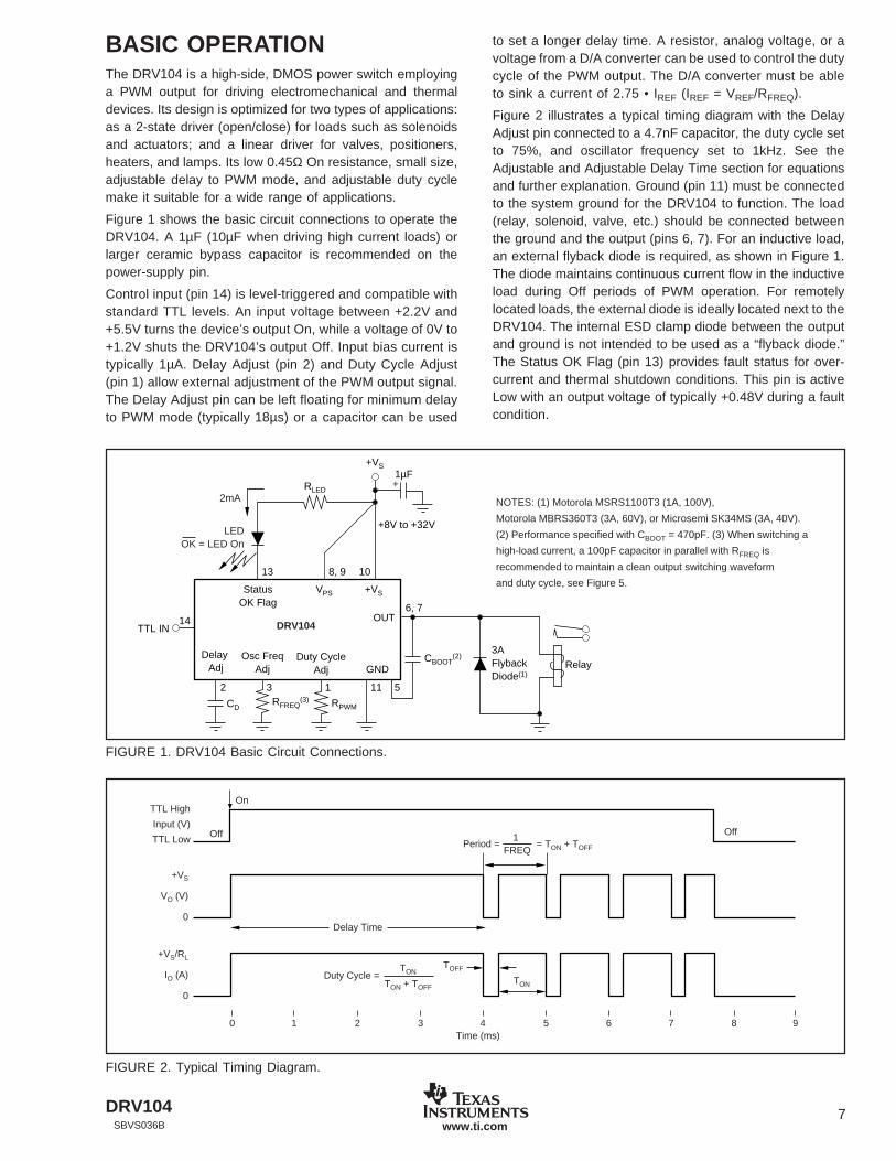
FIGURE 1. DRV104 Basic Circuit Connections.
BASIC OPERATIONThe DRV104 is a high-side, DMOS power switch employinga PWM output for driving electromechanical and thermaldevices. Its design is optimized for two types of applications:as a 2-state driver (open/close) for loads such as solenoidsand actuators; and a linear driver for valves, positioners,heaters, and lamps. Its low 0.45Ω On resistance, small size,adjustable delay to PWM mode, and adjustable duty cyclemake it suitable for a wide range of applications.
Figure 1 shows the basic circuit connections to operate theDRV104. A 1µF (10µF when driving high current loads) orlarger ceramic bypass capacitor is recommended on thepower-supply pin.
Control input (pin 14) is level-triggered and compatible withstandard TTL levels. An input voltage between +2.2V and+5.5V turns the device’s output On, while a voltage of 0V to+1.2V shuts the DRV104’s output Off. Input bias current istypically 1µA. Delay Adjust (pin 2) and Duty Cycle Adjust(pin 1) allow external adjustment of the PWM output signal.The Delay Adjust pin can be left floating for minimum delayto PWM mode (typically 18µs) or a capacitor can be used
to set a longer delay time. A resistor, analog voltage, or avoltage from a D/A converter can be used to control the dutycycle of the PWM output. The D/A converter must be ableto sink a current of 2.75 • IREF (IREF = VREF/RFREQ).
Figure 2 illustrates a typical timing diagram with the DelayAdjust pin connected to a 4.7nF capacitor, the duty cycle setto 75%, and oscillator frequency set to 1kHz. See theAdjustable and Adjustable Delay Time section for equationsand further explanation. Ground (pin 11) must be connectedto the system ground for the DRV104 to function. The load(relay, solenoid, valve, etc.) should be connected betweenthe ground and the output (pins 6, 7). For an inductive load,an external flyback diode is required, as shown in Figure 1.The diode maintains continuous current flow in the inductiveload during Off periods of PWM operation. For remotelylocated loads, the external diode is ideally located next to theDRV104. The internal ESD clamp diode between the outputand ground is not intended to be used as a “flyback diode.”The Status OK Flag (pin 13) provides fault status for over-current and thermal shutdown conditions. This pin is activeLow with an output voltage of typically +0.48V during a faultcondition.
Delay Adj
CD RPWM
TTL IN
RelayCBOOT
(2)
+VS
GND
OUT
+VSStatusOK Flag
3AFlybackDiode(1)
+8V to +32V
Osc FreqAdj
Duty CycleAdj
RFREQ(3)
DRV104
11 5132
146, 7
1013
VPS
8, 9
RLED
LEDOK = LED On
2mA
1µF+
NOTES: (1) Motorola MSRS1100T3 (1A, 100V),
Motorola MBRS360T3 (3A, 60V), or Microsemi SK34MS (3A, 40V).
(2) Performance specified with CBOOT = 470pF. (3) When switching a
high-load current, a 100pF capacitor in parallel with RFREQ is
recommended to maintain a clean output switching waveform
and duty cycle, see Figure 5.
TOFF
TON
On
OffOffPeriod = = TON + TOFF
1FREQ
Duty Cycle = TON
TON + TOFF
Delay Time
+VS
VO (V)
0
+VS/RL
IO (A)
0
TTL High
Input (V)
TTL Low
0 1 2 3 4Time (ms)
5 6 7 8 9
FIGURE 2. Typical Timing Diagram.
DRV1048SBVS036Bwww.ti.com
INITIAL CONSTANTOUTPUT DURATION CD
3µs Pin 2 Tied to +5V18µs Pin 2 Open81µs 100pF
0.81ms 1nF8.1ms 10nF81ms 100nF0.81s 1µF8.1s 10µF
TABLE I. Delay Adjust Times.
FIGURE 3. Simplified Delay Adjust and Frequency Adjust Inputs.
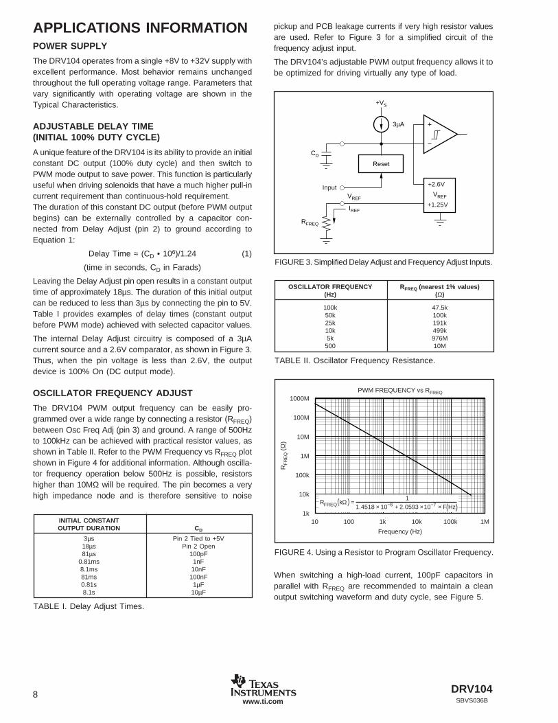
FIGURE 4. Using a Resistor to Program Oscillator Frequency.
OSCILLATOR FREQUENCY RFREQ (nearest 1% values)(Hz) (Ω)
100k 47.5k50k 100k25k 191k10k 499k5k 976M
500 10M
TABLE II. Oscillator Frequency Resistance.
APPLICATIONS INFORMATIONPOWER SUPPLY
The DRV104 operates from a single +8V to +32V supply withexcellent performance. Most behavior remains unchangedthroughout the full operating voltage range. Parameters thatvary significantly with operating voltage are shown in theTypical Characteristics.
ADJUSTABLE DELAY TIME(INITIAL 100% DUTY CYCLE)
A unique feature of the DRV104 is its ability to provide an initialconstant DC output (100% duty cycle) and then switch toPWM mode output to save power. This function is particularlyuseful when driving solenoids that have a much higher pull-incurrent requirement than continuous-hold requirement.The duration of this constant DC output (before PWM outputbegins) can be externally controlled by a capacitor con-nected from Delay Adjust (pin 2) to ground according toEquation 1:
Delay Time ≈ (CD • 106)/1.24 (1)
(time in seconds, CD in Farads)
Leaving the Delay Adjust pin open results in a constant outputtime of approximately 18µs. The duration of this initial outputcan be reduced to less than 3µs by connecting the pin to 5V.Table I provides examples of delay times (constant outputbefore PWM mode) achieved with selected capacitor values.
The internal Delay Adjust circuitry is composed of a 3µAcurrent source and a 2.6V comparator, as shown in Figure 3.Thus, when the pin voltage is less than 2.6V, the outputdevice is 100% On (DC output mode).
OSCILLATOR FREQUENCY ADJUST
The DRV104 PWM output frequency can be easily pro-grammed over a wide range by connecting a resistor (RFREQ)between Osc Freq Adj (pin 3) and ground. A range of 500Hzto 100kHz can be achieved with practical resistor values, asshown in Table II. Refer to the PWM Frequency vs RFREQ plotshown in Figure 4 for additional information. Although oscilla-tor frequency operation below 500Hz is possible, resistorshigher than 10MΩ will be required. The pin becomes a veryhigh impedance node and is therefore sensitive to noise
3µA
CD
RFREQ
VREF
IREF
+VS
VREF
Reset
+2.6V
+1.25V
Input
1000M
100M
10M
1M
100k
10k
1k100 1k10
RF
RE
Q (
Ω)
10k 100k 1M
PWM FREQUENCY vs RFREQ
Frequency (Hz)
RFREQ kΩ( ) =1
1.4518 × 10⁻⁶ + 2.0593 ×10⁻⁷ × F Hz( )
When switching a high-load current, 100pF capacitors inparallel with RFREQ are recommended to maintain a cleanoutput switching waveform and duty cycle, see Figure 5.
pickup and PCB leakage currents if very high resistor valuesare used. Refer to Figure 3 for a simplified circuit of thefrequency adjust input.
The DRV104’s adjustable PWM output frequency allows it tobe optimized for driving virtually any type of load.

DRV104 9SBVS036B www.ti.com
DUTY CYCLE RPWM (Ω) (Nearest 1% Values)
(%) 5kHz 25kHz 100kHz
10 412k 84.5k 25.5k20 487k 97.6k 28.7k30 562k 113k 31.6k40 649k 130k 35.7k50 715k 147k 39.2k60 787k 162k 43.2k70 887k 174k 44.9k80 953k 191k —90 1050k 205k —
FIGURE 6. Using a Resistor to Program Duty Cycle.FIGURE 5. Output Waveform at High Load Current.
FIGURE 7. Using a Voltage to Program Duty Cycle.
DUTY CYCLE VPWM(%) (V)
10 1.50120 1.77340 2.29660 2.81380 3.33790 3.589
TABLE IV. Duty Cycle Adjust Voltage.
TABLE III. Duty Cycle Adjust Resistance.
ADJUSTABLE DUTY CYCLE (PWM MODE)
The DRV104’s externally adjustable duty cycle provides anaccurate means of controlling power delivered to a load.Duty cycle can be set over a range of 10% to 90% with anexternal resistor, analog voltage, or the voltage output of aD/A converter. A low duty cycle results in reduced powerdissipation in the load. This keeps the DRV104 and the loadcooler, resulting in increased reliability for both devices.
Resistor Controlled Duty Cycle
Duty cycle is easily programmed by connecting a resistor(RPWM) between Duty Cycle Adjust (pin 1) and ground. Highresistor values correspond to high duty cycles. At 100kHz,the range of adjustable duty cycle is limited to 10% to 70%.Table III provides resistor values for typical duty cycles.Resistor values for additional duty cycles can be obtainedfrom Figure 6.
Voltage Controlled Duty Cycle
The duty cycle can also be programmed by analog voltageVPWM. With VPWM ≈ 3.59V, the duty cycle is about 90%.Decreasing this voltage results in decreased duty cycles. TableIV provides VPWM values for typical duty cycles. Figure 7 showsthe relationship of duty cycle versus VPWM and its linearity.
10M
1M
100k
10k20 400
RP
WM
(Ω
)
60 80 100
DUTY CYCLE vs RPWM
Duty Cycle (%)
5kHz
25kHz
100kHz
RPWM (kΩ) = 334.35 + 7.75(%DC)
RPWM (kΩ) = 68.73 + 1.52(%DC)
RPWM (kΩ) = 20.62 + 0.39(%DC)
RFREQonly
With100pF inParallelwith RFREQ
Time (10µs)
100
90
80
70
60
50
40
30
20
10
021
Dut
y C
ycle
(%
)2.0
1.5
1.0
0.5
0
–0.5
–1.0
–1.5
–2.0
Dut
y C
ycle
Err
or (
%)
3 4
DUTY CYCLE AND DUTY CYCLE ERRORvs VOLTAGE
VPWM (V)
Duty Cycle
Duty Cycle Error
At VS = 24V and F = 25kHz: VPWM = 1.25 + 0.026 × %DC

DRV10410SBVS036Bwww.ti.com
FIGURE 9. Non-Latching Fault Monitoring Circuit.
FIGURE 10. Latching Fault Monitoring Circuit.
FIGURE 11. Using an LED to Indicate a Fault Condition.
FIGURE 8. Simplified Duty Cycle Adjust Input.
The Duty Cycle Adjust pin is internally driven by an oscillatorfrequency dependent current source and connects to theinput of a comparator, as shown in Figure 8. The DRV104’sPWM adjustment is inherently monotonic; that is, a de-creased voltage (or resistor value) always produces andecreased duty cycle.
STATUS OK FLAG
The Status OK Flag (pin 13) provides a fault indication forover-current and thermal shutdown conditions. During a faultcondition, the Status OK Flag output is driven Low (pinvoltage typically drops to 0.45V). A pull-up resistor, as shownin Figure 9, is required to interface with standard logic. Figure9 also gives an example of a non-latching fault monitoringcircuit, while Figure 10 provides a latching version. TheStatus OK Flag pin can sink up to 10mA, sufficient to driveexternal logic circuitry, a reed relay, or an LED (as shown inFigure 11) to indicate when a fault has occurred. In addition,the Status OK Flag pin can be used to turn off otherDRV104s in a system for chain fault protection.
Over-Current Fault
An over-current fault occurs when the PWM peak outputcurrent is greater than typically 2.0A. The Status OK flag isnot latched. Since current during PWM mode is switched onand off, the Status OK flag output will be modulated withPWM timing (see the Status OK flag waveforms in theTypical Characteristics).
Avoid adding capacitance to pins 6, 7 (OUT) because thiscan cause momentary current limiting.
Over-Temperature Fault
A thermal fault occurs when the die reaches approximately160°C, producing an effect similar to pulling the input low.Internal shutdown circuitry disables the output. The StatusOK Flag is latched in the Low state (fault condition) until thedie has cooled to approximately 140°C.
2.75 • IREF
RPWM
+VS
OSC3.9V
1.3V
13
20kΩ
+5V
Q
Q
CLR
OK
OK
OK Reset
J
CLK
GND K
VS
74XX76A
(1)
NOTE: (1) A small capacitor (10pF) may be required in noisy environments.
DRV104
Thermal ShutdownOver-Current
8, 9VPS
6, 7OUT
PWM
Status OK Flag
5kΩ
+5V
Status OK Flag
(LED)HLMP-Q156
13
DRV104
Thermal ShutdownOver-Current
6, 7
8, 9VPS
OUT
PWM
DRV104
Thermal ShutdownOver-Current
PWM
6, 7
8, 913
OUT
VPS
5kΩPull-Up
+5V
Status OK Flag
TTL or HCT
DRV104 11SBVS036B www.ti.com
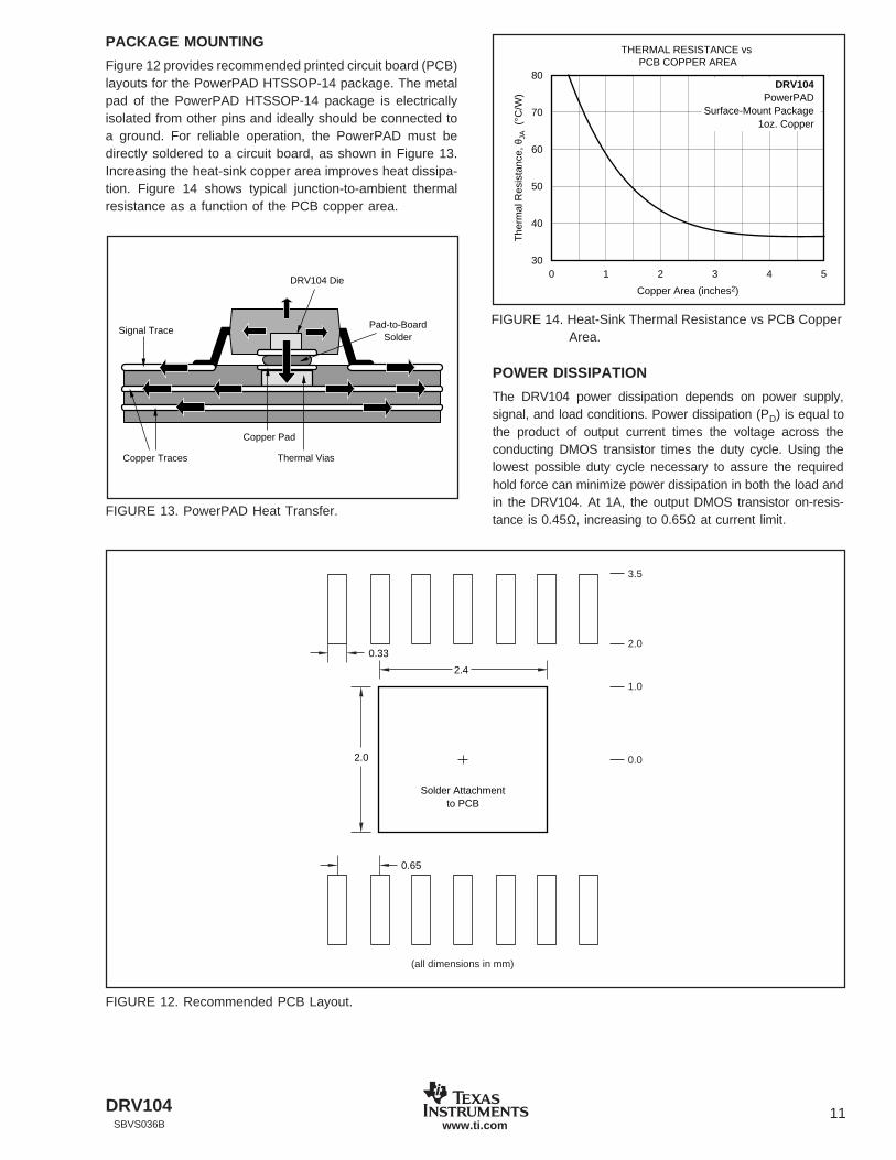
FIGURE 12. Recommended PCB Layout.
FIGURE 13. PowerPAD Heat Transfer.
FIGURE 14. Heat-Sink Thermal Resistance vs PCB CopperArea.
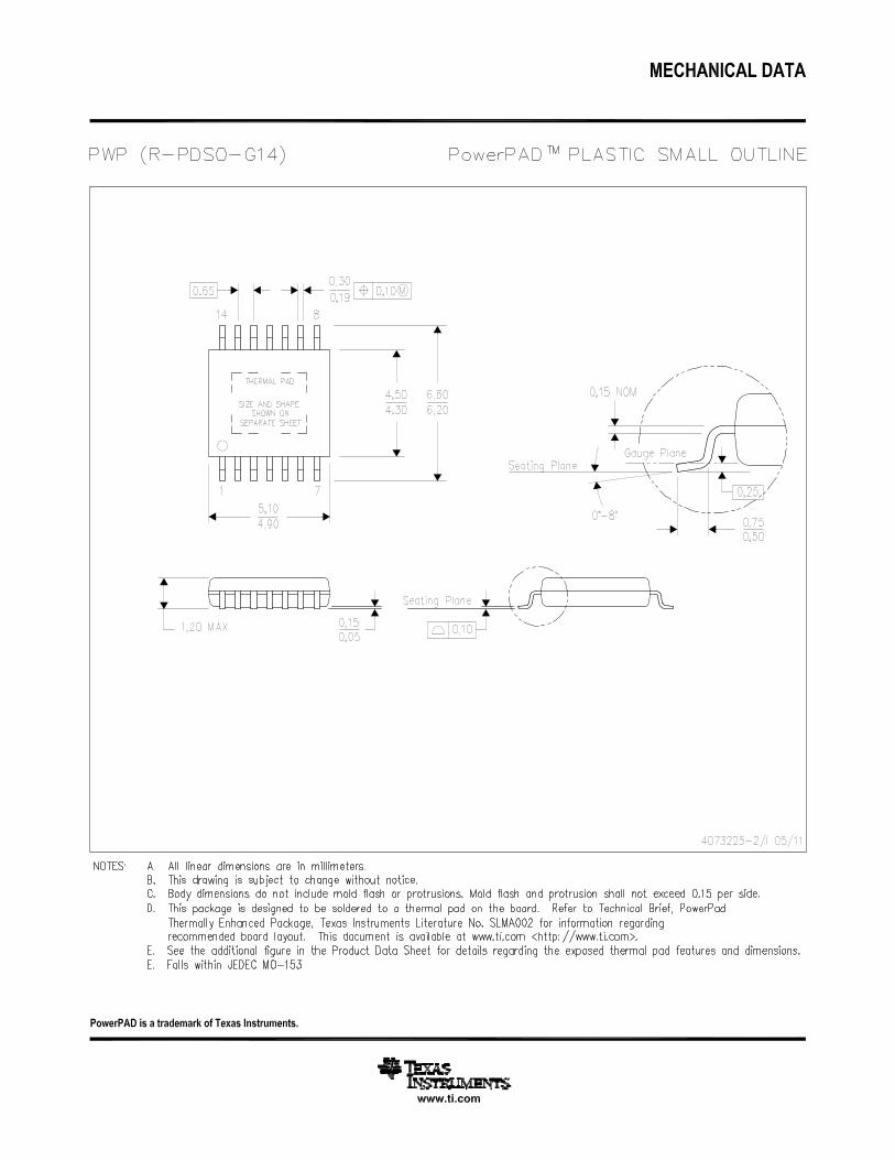
PACKAGE MOUNTING
Figure 12 provides recommended printed circuit board (PCB)layouts for the PowerPAD HTSSOP-14 package. The metalpad of the PowerPAD HTSSOP-14 package is electricallyisolated from other pins and ideally should be connected toa ground. For reliable operation, the PowerPAD must bedirectly soldered to a circuit board, as shown in Figure 13.Increasing the heat-sink copper area improves heat dissipa-tion. Figure 14 shows typical junction-to-ambient thermalresistance as a function of the PCB copper area.
POWER DISSIPATION
The DRV104 power dissipation depends on power supply,signal, and load conditions. Power dissipation (PD) is equal tothe product of output current times the voltage across theconducting DMOS transistor times the duty cycle. Using thelowest possible duty cycle necessary to assure the requiredhold force can minimize power dissipation in both the load andin the DRV104. At 1A, the output DMOS transistor on-resis-tance is 0.45Ω, increasing to 0.65Ω at current limit.
Solder Attachmentto PCB
2.0
0.33
2.4
0.65
0.0
1.0
2.0
3.5
(all dimensions in mm)
Copper Traces
Signal Trace
Copper Pad
Thermal Vias
DRV104 Die
Pad-to-BoardSolder
THERMAL RESISTANCE vs PCB COPPER AREA
80
70
60
50
40
30
The
rmal
Res
ista
nce,
θJA
(°C
/W)
0 1 2 3 4 5
Copper Area (inches2)
DRV104PowerPAD
Surface-Mount Package1oz. Copper

DRV10412SBVS036Bwww.ti.com
At very high oscillator frequencies, the energy in the DRV104’slinear rise and fall times can become significant and causean increase in PD.
THERMAL PROTECTION
Power dissipated in the DRV104 causes its internal junctiontemperature to rise. The DRV104 has an on-chip thermalshutdown circuitry that protects the IC from damage. Thethermal protection circuitry disables the output when thejunction temperature reaches approximately +160°C, allow-ing the device to cool. When the junction temperature coolsto approximately +140°C, the output circuitry is again en-abled. Depending on load and signal conditions, the thermalprotection circuit may cycle on and off. This limits the dissi-pation of the driver but may have an undesirable effect on theload.
Any tendency to activate the thermal protection circuit indi-cates excessive power dissipation or an inadequate heatsink. For reliable operation, junction temperature should belimited to a maximum of +125°C. To estimate the margin ofsafety in a complete design (including heat-sink), increasethe ambient temperature until the thermal protection is trig-gered. Use worst-case load and signal conditions. For goodreliability, thermal protection should trigger more than 35°Cabove the maximum expected ambient condition of yourapplication. This produces a junction temperature of 125°Cat the maximum expected ambient condition.
The internal protection circuitry of the DRV104 is designed toprotect against overload conditions. It is not intended toreplace proper heat sinking. Continuously running the DRV104into thermal shutdown will degrade device reliability.
HEAT SINKING
Most applications do not require a heat-sink to assure thatthe maximum operating junction temperature (125°C) is notexceeded. However, junction temperature should be kept aslow as possible for increased reliability. Junction temperaturecan be determined according to the following equations:
TJ = TA + PDθJA (3)
θJA = θJC + θCH + θHA (4)
where:
TJ = Junction Temperature (°C)
TA = Ambient Temperature (°C)
PD = Power Dissipated (W)
θJC = Junction-to-Case Thermal Resistance (°C/W)
θCH = Case-to-Heat Sink Thermal Resistance (°C/W)
θHA = Heat Sink-to-Ambient Thermal Resistance (°C/W)
θJA = Junction-to-Air Thermal Resistance (°C/W)
Using a heat sink significantly increases the maximum allow-able power dissipation at a given ambient temperature.
The answer to the question of selecting a heat-sink lies indetermining the power dissipated by the DRV104. For DCoutput into a purely resistive load, power dissipation is simplythe load current times the voltage developed across theconducting output transistor times the duty cycle. Other loadsare not as simple. (For further information on calculatingpower dissipation, refer to Application Bulletin SBFA002,available at www.ti.com.) Once power dissipation for anapplication is known, the proper heat-sink can be selected.
Heat-Sink Selection Example
A PowerPAD HTSSOP-14 package dissipates 2W. The maxi-mum expected ambient temperature is 35°C. Find the properheat-sink to keep the junction temperature below 125°C.
Combining Equations 1 and 2 gives:
TJ = TA + PD(θJC + θCH + θHA) (5)
TJ, TA, and PD are given. θJC is provided in the specificationtable: 2.07°C/W. θCH depends on heat sink size, area, andmaterial used. Semiconductor package type and mounting canalso affect θCH. A typical θCH for a soldered-in-place PowerPADHTSSOP-14 package is 2°C/W. Now, solving for θHA:
θ θ θ
θ
θ
HAJ A
DJC CH
HA
HA
T TP
C CW
C W C W
C W
= +( )
= ° ° ° + °( )
= °
––
–– . / /
. /
125 352
2 07 2
40 9
(6)
To maintain junction temperature below 125°C, the heat-sinkselected must have a θHA less than 40.9°C/W. In otherwords, the heat-sink temperature rise above ambient tem-perature must be less than 81.8°C (40.9°C/W • 2W).
Another variable to consider is natural convection versusforced convection air flow. Forced-air cooling by a small fancan lower θCA (θCH + θHA) dramatically.
As mentioned above, once a heat-sink has been selected,the complete design should be tested under worst-case loadand signal conditions to ensure proper thermal protection.
RFI/EMI
Any switching system can generate noise and interferenceby radiation or conduction. The DRV104 is designed withcontrolled slew rate current switching to reduce these effects.By slowing the rise time of the output to 1µs, much lowerswitching noise is generated.
Radiation from the DRV104-to-load wiring (the antenna ef-fect) can be minimized by using twisted pair cable or byshielding. Good PCB ground planes are recommended forlow noise and good heat dissipation. Refer to the Bypassingsection for notes on placement of the flyback diode.
DRV104 13SBVS036B www.ti.com
BYPASSING
A 1µF ceramic bypass capacitor is adequate for uniform dutycycle control when switching loads of less than 0.5A. Largerbypass capacitors are required when switching high-currentloads. A 10µF ceramic capacitor is recommended for heavy-duty (1.2A) applications. It may also be desirable to run theDRV104 and load driver on separate power supplies at high-load currents. Bypassing is especially critical near the abso-lute maximum supply voltage of 32V. In the event of a currentoverload, the DRV104 current limit responds in microsec-onds, dropping the load current to zero. With inadequatebypassing, energy stored in the supply line inductance canlift the supply sufficiently to exceed voltage breakdown withcatastrophic results.
Place the flyback diode at the DRV104 end when driving long(inductive) cables to a remotely located load. This minimizesRFI/EMI and helps protect the output DMOS transistor frombreakdown caused by dI/dt transients. Fast rectifier diodessuch as epitaxial silicon or Schottky types are recommendedfor use as flyback diodes.
APPLICATIONS CIRCUITSSINGLE AND MULTICHANNEL
The DRV104 can be used in a variety of ways with resistiveand inductive loads. As a single-channel driver, it can beplaced on one PC board or inside a solenoid, relay, actuator,valve, motor, heater, thermoelectric cooler, or lamp housing.In high-density systems, multichannel power drivers may bepacked close together on a PC board. For these switchingapplications, it is important to provide power supply bypass-ing as close to the driver IC as possible to avoid cross-coupling of spikes from one circuit to another. Also, in someapplications, it may be necessary to keep beat frequencies(sum and difference between DRV oscillators or betweenDRV oscillators and system clock frequencies) from interfer-ing with low-level analog circuits that are located relativelynear to the power drivers. Paralleling device outputs is notrecommended as unequal load sharing and device damagewill result.
BEAT FREQUENCIES IN NON-SYNCHRONIZEDMULTICHANNEL SYSTEMS
In many multichannel systems, beat frequencies are of noconsequence where each DRV uses its own internal oscilla-tor.
Beat frequencies can be intentionally set up to be outside themeasurement base-band to avoid interference in sensitiveanalog circuits located nearby. For example, with two
DRV104s, a beat frequency of 22.5kHz can be establishedby setting one internal oscillator to a center of 62.5kHz andthe other to 40kHz. Considering the specification of ±20%frequency accuracy, the beat could range from 2kHz (48kHzand 50kHz) to 43kHz (75kHz and 32kHz). By limiting theanalog measurement bandwidth to 100Hz, for example,interference can be avoided.
BEAT FREQUENCY ELIMINATION—OPTIONALSYNCHRONIZATION
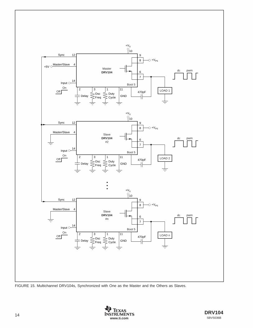
The benefit of synchronization in multichannel systems isthat measurement interference can be avoided in low-levelanalog circuits, particularly when physically close to theDRVs. Specifically, synchronization will accomplish the fol-lowing:
1. Eliminate beat frequencies between DRVs or DRVs andthe system clock.
2. Predict quiet or non-switching times.
Synchronization of DRV104s is possible by using one oscil-lator frequency for all DRVs. See Figure 15 for an exampleof one DRV internal oscillator as the master and the othersas slaves. Also, one external clock can be used as themaster and all the others as slaves.
PEAK SUPPLY CURRENT ELIMINATION—OPTIONALSWITCHING SKEW
In many systems, particularly where only a few channels areused or low magnitude load currents are present, it isunnecessary to skew the switching times.
In some multichannel systems, where just PWM is used,without initial dc time delay, simultaneous switching of edgescan cause large peak currents to be drawn from the mainpower supply. This is similar to that which occurs whenmultiple switching power supplies draw current from onepower source.
Peak currents can be reduced by synchronizing oscillatorsand skewing switching edges. Synchronization has the addedbenefit of eliminating beat frequencies, as discussed above.
Skewing can be accomplished by using a polyphase clockapproach, which intentionally delays the time that each DRVswitches on PWM edges.
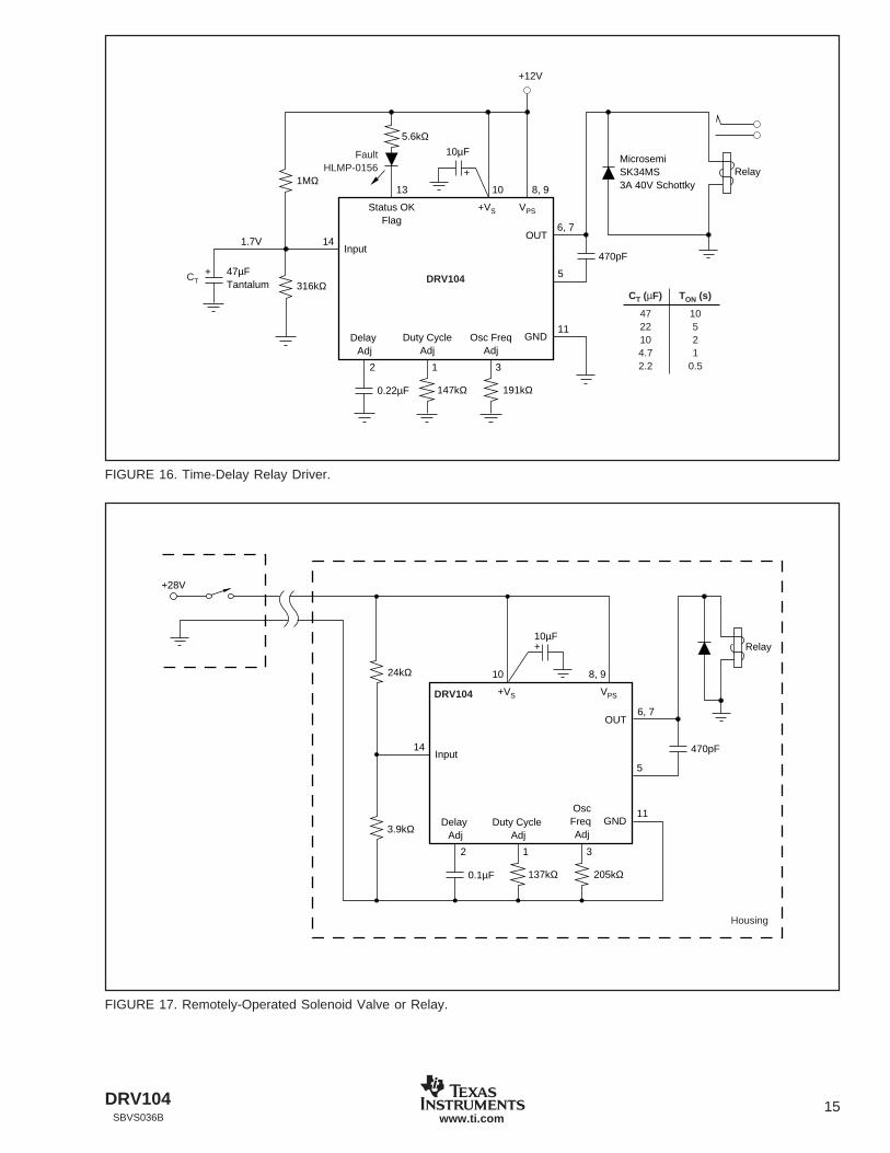
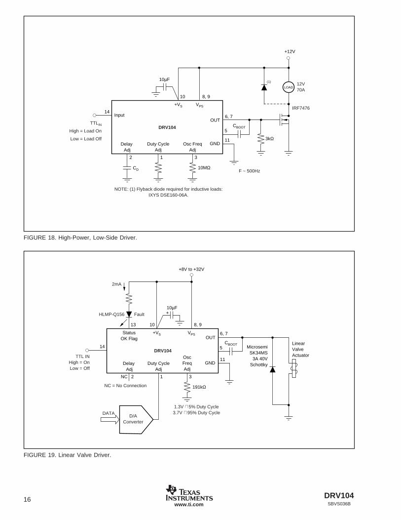
The DRV104 is useful for a variety of relay driver applications(see Figures 16 and 17), as well as valve drivers (see Figures18 and 19).
DRV10414SBVS036Bwww.ti.com
Delay DutyCycle
OscFreq
470pF
MasterDRV104
13
GND
112
4+5V
14
12
Master/Slave
Sync
+VS
+VPS
Input
8
7
9
6
10
OnOff LOAD 1
dc pwm
Delay DutyCycle
OscFreq
SlaveDRV104
#2
13
GND
112
4
14
12
Master/Slave
Sync
+VS
+VPS
Input
8
7
9
6
10
OnOff LOAD 2
dc pwm
Delay DutyCycle
OscFreq
SlaveDRV104
#n
13
GND
112
4
14
12
Master/Slave
Sync
+VS
+VPS
Input
8
7
9
6
10
OnOff LOAD n
dc pwm
…470pF
470pF
Boot 5
Boot 5
Boot 5
FIGURE 15. Multichannel DRV104s, Synchronized with One as the Master and the Others as Slaves.
DRV104 15SBVS036B www.ti.com
FIGURE 16. Time-Delay Relay Driver.
Delay Adj
0.22µF 191kΩ
+12V
GND
OUTInput
Status OKFlag
MicrosemiSK34MS3A 40V Schottky
Duty CycleAdj
Osc FreqAdj
147kΩ
470pF
47µFTantalum DRV104
11
5
312
141.7V6, 7
13
VPS
8, 91MΩ
316kΩ
FaultHLMP-0156
+VS
10µF
10
+
+CT
CT (µF)
4722104.72.2
TON (s)
10521
0.5
5.6kΩ
Relay
Delay Adj
Duty Cycle Adj
OscFreq Adj
0.1µF 205kΩ
GND
OUT
Input
137kΩ
470pF
DRV104
11
312
14
6, 7
24kΩ
3.9kΩ
VPS
8, 9
+28V
5
Housing
Relay
+VS
10µF
10
+
FIGURE 17. Remotely-Operated Solenoid Valve or Relay.
DRV10416SBVS036Bwww.ti.com
FIGURE 18. High-Power, Low-Side Driver.
Delay Adj
CD 10MΩ
+12V
GND
OUTInput
Duty CycleAdj
Osc FreqAdj
CBOOT
3kΩ
DRV104
11
5
312
146, 7
VPS
8, 9
+VS
10µF
10
TTLIN
High = Load On
Low = Load Off
NOTE: (1) Flyback diode required for inductive loads:IXYS DSE160-06A.
F ~ 500Hz
IRF7476
(1) 12V70A
LOAD
FIGURE 19. Linear Valve Driver.
LinearValveActuator
OUT6, 7
14
2 1 3NC
13
11
StatusOK Flag
+8V to +32V
DRV104Microsemi
SK34MS3A 40V
Schottky
8, 9
VPS
HLMP-Q156 Fault
2mA
Delay Adj
191kΩ
GNDDuty CycleAdj
OscFreqAdj
TTL INHigh = OnLow = Off
10
+VS
10µF
CBOOT
+
1.3V ≅ 5% Duty Cycle3.7V ≅ 95% Duty Cycle
D/AConverter
DATA
NC = No Connection
5
PACKAGE OPTION ADDENDUM
www.ti.com 24-Aug-2018
Addendum-Page 1
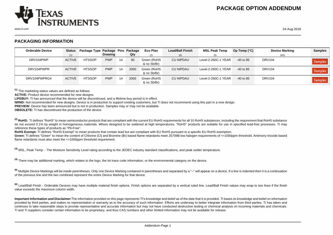
PACKAGING INFORMATION
Orderable Device Status(1)
Package Type PackageDrawing
Pins PackageQty
Eco Plan(2)
Lead/Ball Finish(6)
MSL Peak Temp(3)
Op Temp (°C) Device Marking(4/5)
Samples
DRV104PWP ACTIVE HTSSOP PWP 14 90 Green (RoHS& no Sb/Br)
CU NIPDAU Level-2-260C-1 YEAR -40 to 85 DRV104
DRV104PWPR ACTIVE HTSSOP PWP 14 2000 Green (RoHS& no Sb/Br)
CU NIPDAU Level-2-260C-1 YEAR -40 to 85 DRV104
DRV104PWPRG4 ACTIVE HTSSOP PWP 14 2000 Green (RoHS& no Sb/Br)
CU NIPDAU Level-2-260C-1 YEAR -40 to 85 DRV104
(1) The marketing status values are defined as follows:ACTIVE: Product device recommended for new designs.LIFEBUY: TI has announced that the device will be discontinued, and a lifetime-buy period is in effect.NRND: Not recommended for new designs. Device is in production to support existing customers, but TI does not recommend using this part in a new design.PREVIEW: Device has been announced but is not in production. Samples may or may not be available.OBSOLETE: TI has discontinued the production of the device.
(2) RoHS: TI defines "RoHS" to mean semiconductor products that are compliant with the current EU RoHS requirements for all 10 RoHS substances, including the requirement that RoHS substancedo not exceed 0.1% by weight in homogeneous materials. Where designed to be soldered at high temperatures, "RoHS" products are suitable for use in specified lead-free processes. TI mayreference these types of products as "Pb-Free".RoHS Exempt: TI defines "RoHS Exempt" to mean products that contain lead but are compliant with EU RoHS pursuant to a specific EU RoHS exemption.Green: TI defines "Green" to mean the content of Chlorine (Cl) and Bromine (Br) based flame retardants meet JS709B low halogen requirements of <=1000ppm threshold. Antimony trioxide basedflame retardants must also meet the <=1000ppm threshold requirement.
(3) MSL, Peak Temp. - The Moisture Sensitivity Level rating according to the JEDEC industry standard classifications, and peak solder temperature.
(4) There may be additional marking, which relates to the logo, the lot trace code information, or the environmental category on the device.
(5) Multiple Device Markings will be inside parentheses. Only one Device Marking contained in parentheses and separated by a "~" will appear on a device. If a line is indented then it is a continuationof the previous line and the two combined represent the entire Device Marking for that device.
(6) Lead/Ball Finish - Orderable Devices may have multiple material finish options. Finish options are separated by a vertical ruled line. Lead/Ball Finish values may wrap to two lines if the finishvalue exceeds the maximum column width.
Important Information and Disclaimer:The information provided on this page represents TI's knowledge and belief as of the date that it is provided. TI bases its knowledge and belief on informationprovided by third parties, and makes no representation or warranty as to the accuracy of such information. Efforts are underway to better integrate information from third parties. TI has taken andcontinues to take reasonable steps to provide representative and accurate information but may not have conducted destructive testing or chemical analysis on incoming materials and chemicals.TI and TI suppliers consider certain information to be proprietary, and thus CAS numbers and other limited information may not be available for release.

PACKAGE OPTION ADDENDUM
www.ti.com 24-Aug-2018
Addendum-Page 2
In no event shall TI's liability arising out of such information exceed the total purchase price of the TI part(s) at issue in this document sold by TI to Customer on an annual basis.

TAPE AND REEL INFORMATION
*All dimensions are nominal
Device PackageType
PackageDrawing
Pins SPQ ReelDiameter
(mm)
ReelWidth
W1 (mm)
A0(mm)
B0(mm)
K0(mm)
P1(mm)
W(mm)
Pin1Quadrant
DRV104PWPR HTSSOP PWP 14 2000 330.0 12.4 6.9 5.6 1.6 8.0 12.0 Q1
PACKAGE MATERIALS INFORMATION
www.ti.com 12-Dec-2015
Pack Materials-Page 1
*All dimensions are nominal
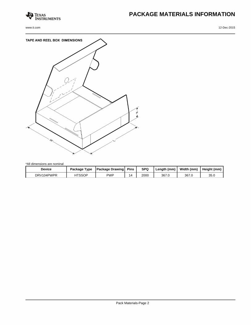
Device Package Type Package Drawing Pins SPQ Length (mm) Width (mm) Height (mm)
DRV104PWPR HTSSOP PWP 14 2000 367.0 367.0 35.0
PACKAGE MATERIALS INFORMATION
www.ti.com 12-Dec-2015
Pack Materials-Page 2
IMPORTANT NOTICE
Texas Instruments Incorporated (TI) reserves the right to make corrections, enhancements, improvements and other changes to itssemiconductor products and services per JESD46, latest issue, and to discontinue any product or service per JESD48, latest issue. Buyersshould obtain the latest relevant information before placing orders and should verify that such information is current and complete.TI’s published terms of sale for semiconductor products (http://www.ti.com/sc/docs/stdterms.htm) apply to the sale of packaged integratedcircuit products that TI has qualified and released to market. Additional terms may apply to the use or sale of other types of TI products andservices.Reproduction of significant portions of TI information in TI data sheets is permissible only if reproduction is without alteration and isaccompanied by all associated warranties, conditions, limitations, and notices. TI is not responsible or liable for such reproduceddocumentation. Information of third parties may be subject to additional restrictions. Resale of TI products or services with statementsdifferent from or beyond the parameters stated by TI for that product or service voids all express and any implied warranties for theassociated TI product or service and is an unfair and deceptive business practice. TI is not responsible or liable for any such statements.Buyers and others who are developing systems that incorporate TI products (collectively, “Designers”) understand and agree that Designersremain responsible for using their independent analysis, evaluation and judgment in designing their applications and that Designers havefull and exclusive responsibility to assure the safety of Designers' applications and compliance of their applications (and of all TI productsused in or for Designers’ applications) with all applicable regulations, laws and other applicable requirements. Designer represents that, withrespect to their applications, Designer has all the necessary expertise to create and implement safeguards that (1) anticipate dangerousconsequences of failures, (2) monitor failures and their consequences, and (3) lessen the likelihood of failures that might cause harm andtake appropriate actions. Designer agrees that prior to using or distributing any applications that include TI products, Designer willthoroughly test such applications and the functionality of such TI products as used in such applications.TI’s provision of technical, application or other design advice, quality characterization, reliability data or other services or information,including, but not limited to, reference designs and materials relating to evaluation modules, (collectively, “TI Resources”) are intended toassist designers who are developing applications that incorporate TI products; by downloading, accessing or using TI Resources in anyway, Designer (individually or, if Designer is acting on behalf of a company, Designer’s company) agrees to use any particular TI Resourcesolely for this purpose and subject to the terms of this Notice.TI’s provision of TI Resources does not expand or otherwise alter TI’s applicable published warranties or warranty disclaimers for TIproducts, and no additional obligations or liabilities arise from TI providing such TI Resources. TI reserves the right to make corrections,enhancements, improvements and other changes to its TI Resources. TI has not conducted any testing other than that specificallydescribed in the published documentation for a particular TI Resource.Designer is authorized to use, copy and modify any individual TI Resource only in connection with the development of applications thatinclude the TI product(s) identified in such TI Resource. NO OTHER LICENSE, EXPRESS OR IMPLIED, BY ESTOPPEL OR OTHERWISETO ANY OTHER TI INTELLECTUAL PROPERTY RIGHT, AND NO LICENSE TO ANY TECHNOLOGY OR INTELLECTUAL PROPERTYRIGHT OF TI OR ANY THIRD PARTY IS GRANTED HEREIN, including but not limited to any patent right, copyright, mask work right, orother intellectual property right relating to any combination, machine, or process in which TI products or services are used. Informationregarding or referencing third-party products or services does not constitute a license to use such products or services, or a warranty orendorsement thereof. Use of TI Resources may require a license from a third party under the patents or other intellectual property of thethird party, or a license from TI under the patents or other intellectual property of TI.TI RESOURCES ARE PROVIDED “AS IS” AND WITH ALL FAULTS. TI DISCLAIMS ALL OTHER WARRANTIES ORREPRESENTATIONS, EXPRESS OR IMPLIED, REGARDING RESOURCES OR USE THEREOF, INCLUDING BUT NOT LIMITED TOACCURACY OR COMPLETENESS, TITLE, ANY EPIDEMIC FAILURE WARRANTY AND ANY IMPLIED WARRANTIES OFMERCHANTABILITY, FITNESS FOR A PARTICULAR PURPOSE, AND NON-INFRINGEMENT OF ANY THIRD PARTY INTELLECTUALPROPERTY RIGHTS. TI SHALL NOT BE LIABLE FOR AND SHALL NOT DEFEND OR INDEMNIFY DESIGNER AGAINST ANY CLAIM,INCLUDING BUT NOT LIMITED TO ANY INFRINGEMENT CLAIM THAT RELATES TO OR IS BASED ON ANY COMBINATION OFPRODUCTS EVEN IF DESCRIBED IN TI RESOURCES OR OTHERWISE. IN NO EVENT SHALL TI BE LIABLE FOR ANY ACTUAL,DIRECT, SPECIAL, COLLATERAL, INDIRECT, PUNITIVE, INCIDENTAL, CONSEQUENTIAL OR EXEMPLARY DAMAGES INCONNECTION WITH OR ARISING OUT OF TI RESOURCES OR USE THEREOF, AND REGARDLESS OF WHETHER TI HAS BEENADVISED OF THE POSSIBILITY OF SUCH DAMAGES.Unless TI has explicitly designated an individual product as meeting the requirements of a particular industry standard (e.g., ISO/TS 16949and ISO 26262), TI is not responsible for any failure to meet such industry standard requirements.Where TI specifically promotes products as facilitating functional safety or as compliant with industry functional safety standards, suchproducts are intended to help enable customers to design and create their own applications that meet applicable functional safety standardsand requirements. Using products in an application does not by itself establish any safety features in the application. Designers mustensure compliance with safety-related requirements and standards applicable to their applications. Designer may not use any TI products inlife-critical medical equipment unless authorized officers of the parties have executed a special contract specifically governing such use.Life-critical medical equipment is medical equipment where failure of such equipment would cause serious bodily injury or death (e.g., lifesupport, pacemakers, defibrillators, heart pumps, neurostimulators, and implantables). Such equipment includes, without limitation, allmedical devices identified by the U.S. Food and Drug Administration as Class III devices and equivalent classifications outside the U.S.TI may expressly designate certain products as completing a particular qualification (e.g., Q100, Military Grade, or Enhanced Product).Designers agree that it has the necessary expertise to select the product with the appropriate qualification designation for their applicationsand that proper product selection is at Designers’ own risk. Designers are solely responsible for compliance with all legal and regulatoryrequirements in connection with such selection.Designer will fully indemnify TI and its representatives against any damages, costs, losses, and/or liabilities arising out of Designer’s non-compliance with the terms and provisions of this Notice.
Mailing Address: Texas Instruments, Post Office Box 655303, Dallas, Texas 75265Copyright © 2018, Texas Instruments Incorporated