
120 mm DVD - Read-Only Disk - Ecma International · Standard ECMA-268 specifies a 80 mm DVD -...
96
Standard ECMA-267 3rd Edition - April 2001 Standardizing Information and Communication Systems Phone: +41 22 849.60.00 - Fax: +41 22 849.60.01 - URL: http://www.ecma.ch - Internet: [email protected] 120 mm DVD - Read-Only Disk
Transcript of 120 mm DVD - Read-Only Disk - Ecma International · Standard ECMA-268 specifies a 80 mm DVD -...

Standard ECMA-267 3rd Edition - April 2001
S t a n d a r d i z i n g I n f o r m a t i o n a n d C o m m u n i c a t i o n S y s t e m s
Phone: +41 22 849 .60 .00 - Fax: +41 22 849 .60 .01 - URL: h t tp : / /www.ecma.ch - In ternet : he [email protected]
120 mm DVD - Read-Only Disk

.

Standard ECMA-267 3rd Edition - April 2001
S t a n d a r d i z i n g I n f o r m a t i o n a n d C o m m u n i c a t i o n S y s t e m s
Phone: +41 22 849 .60 .00 - Fax: +41 22 849 .60 .01 - URL: h t tp : / /www.ecma.ch - In ternet : he [email protected]
MB ECMA-267 25-04-01 16,52
120 mm DVD - Read-Only Disk

.

Brief History
ECMA Technical Committee TC31 was established in 1984 for the standardization of Optical Disks and Optical Disk Cartridges (ODC). Since its establishment, the Committee has made major contributions to ISO/IEC SC23 toward the development of International Standards for 90 mm, 120 mm, 130 mm, 300 mm, and 356 mm media. Numerous standards have been developed by TC31 and published by ECMA, almost all of which have also been adopted by ISO/IEC under the fast-track procedure as International Standards.
In February 1997 a group of ten Companies, known as the DVD Consortium, proposed to TC31 to develop an ECMA Standard for the first member of a family of 120 mm optical disks. TC31 adopted this project and started work on a first ECMA Standard for DVD - Read-Only disks. This ECMA Standard specifies the physical characteristics of such a disks which can be used for video, audio or data applications. A standard for volume and file structure common to these three types of application has been developed in ECMA Technical Committee TC15. Further work has been undertaken for a rewritable disk known as DVD-RAM, for a case for such disks, and for a writable disk DVD-R. This work is supported by nine members of the DVD Forum.
This Standard ECMA-267 specifies four Types of DVD - Read-Only disks with a nominal capacity from 4,7 Gbytes to 17,0 Gbytes. Standard ECMA-268 specifies a 80 mm DVD - Read-Only disk which differs from that of this Standard ECMA-267 only where the relevant parameters depend on the dimension of the diameter. Four Types of such DVD disks with a nominal capacity of 1,46 Gbytes to 5,32 Gbytes are specified. It has been adopted by ISO/IEC JTC 1 as International Standard ISO/IEC 16448.
Adopted as 3rd edition of Standard ECMA-267 by the ECMA General Assembly in April 2001.

.

- i -
Table of contents
Section 1 - General 1
1 Scope 1
2 Conformance 1
2.1 Optical Disk 1 2.2 Generating system 1 2.3 Receiving system 1
3 Reference 1
4 Definitions 1
4.1 Adhesive layer 1 4.2 Channel bit 1 4.3 Clamping Zone 1 4.4 Digital Sum Value (DSV) 2 4.5 Disk Reference Plane 2 4.6 Dual Layer disk 2 4.7 Dummy substrate 2 4.8 Entrance surface 2 4.9 Optical disk 2 4.10 Physical sector number 2 4.11 Read-only disk 2 4.12 Recorded layer 2 4.13 Reed-Solomon code 2 4.14 Reserved field 2 4.15 Sector 2 4.16 Single Layer disk 2 4.17 Spacer 2 4.18 Substrate 2 4.19 Track 2 4.20 Track pitch 3 4.21 Zone 3
5 Conventions and notations 3
5.1 Representation of numbers 3 5.2 Names 3
6 List of acronyms 3
7 General description of the disk 4
8 General requirements 5
8.1 Environments 5
8.1.1 Test environment 5 8.1.2 Operating environment 6 8.1.3 Storage environment 6
8.1.4 Transportation 6
8.2 Safety requirements 6 8.3 Flammability 6

- i i -
9 Reference measurement devices 6
9.1 Pick Up Head (PUH) 6 9.2 Measurement conditions 8 9.3 Normalized servo transfer function 8 9.4 Reference Servo for axial tracking 8 9.5 Reference Servo for radial tracking 9
Section 2 - Dimensional, mechanical and physical characteristics of the disk 10
10 Dimensional characteristics 10
10.1 Overall dimensions 11 10.2 First transition area 11 10.3 Second transition area 11 10.4 Clamping Zone 11 10.5 Third transition area 11 10.6 Information Zone 12
10.6.1 Sub-divisions of the Information Zone 12 10.6.2 Track geometry 12 10.6.3 Track modes 13 10.6.4 Channel bit length 13
10.7 Rim area 13 10.8 Remark on tolerances 13 10.9 Runout 14
10.9.1 Axial runout 14 10.9.2 Radial runout 14
10.10 Label 14
11 Mechanical parameters 14
11.1 Mass 14 11.2 Moment of inertia 14 11.3 Dynamic imbalance 14 11.4 Sense of rotation 14
12 Optical parameters 14
12.1 Index of refraction 14 12.2 Thickness of the transparent substrate 14 12.3 Thickness of the spacer of Types C and D 14 12.4 Angular deviation 15 12.5 Birefringence of the transparent substrate 15 12.6 Reflectivity 15
Section 3 - Operational Signals 18
13 High frequency signals (HF) 18
13.1 Modulated amplitude 18 13.2 Signal asymmetry 19 13.3 Cross-track signal 19 13.4 Quality of signals 19
13.4.1 Jitter 19 13.4.2 Random errors 19 13.4.3 Defects 19

- i i i -
14 Servo signals 19
14.1 Differential phase tracking error signal 20 14.2 Tangential push-pull signal 20
Section 4 - Data Format 22
15 General 22
16 Data Frames (figure 16) 22
16.1 Identification Data (ID) 23 16.2 ID Error Detection Code (IED) 24 16.3 Copyright Management Information (CPR_MAI) 24 16.4 Error Detection Code (EDC) 24
17 Scrambled Frames 25
18 ECC Blocks 25
19 Recording Frames 27
20 Modulation 28
21 Physical Sectors 29
22 Suppress control of the d.c. component 30
Section 5 Format of the Information Zone(s) 31
23 General description of an Information Zone 31
24 Layout of the Information Zone 31
25 Physical Sector numbering 32
26 Lead-in Zone 33
26.1 Initial Zone 34 26.2 Reference Code Zone 34 26.3 Buffer Zone 1 34 26.4 Buffer Zone 2 34 26.5 Control Data Zone 35
26.5.1 Physical format information 35 26.5.2 Disk manufacturing information 37 26.5.3 Content provider information 37
27 Middle Zone 37
28 Lead-out Zone 37
Annex A - Measurement of the angular deviation αααα 39
Annex B - Measurement of birefringence 41
Annex C - Measurement of the differential phase tracking error 43
- iv -
Annex D - Measurement of light reflectance 47
Annex E -Tapered cone for disk clamping 49
Annex F - Measurement of jitter 51
Annex G - 8-to-16 Modulation with RLL (2,10) requirements 55
Annex H - Burst Cutting Area (BCA) 65
Annex J - Source Identification Code (SID) 71
Annex K- Measurement of the thickness of the spacer of Dual Layer disks 75
Annex L - Note on the Reference Code 77
Annex M - Maximum transfer rate 79
Annex N - Disk bonding 81
Annex P - Transportation 83

Section 1 - General
1 Scope This ECMA Standard specifies the mechanical, physical and optical characteristics of a 120 mm, read-only optical disk to enable the interchange of such disks. It specifies the quality of the recorded signals, the format of the data and the recording method, thereby allowing for information interchange by means of such disks. This disk is identified as DVD - Read-Only Disk.
This ECMA Standard specifies
− four related but different Types of this disk (see clause 7),
− the conditions for conformance,
− the environments in which the disk is to be operated and stored,
− the mechanical and physical characteristics of the disk, so as to provide mechanical interchange between data processing systems,
− the format of the information on the disk, including the physical disposition of the tracks and sectors, the error correcting codes and the coding method used,
− the characteristics of the signals recorded on the disk, enabling data processing systems to read the data from the disk.
This ECMA Standard provides for interchange of disks between disk drives. Together with a standard for volume and file structure, it provides for full data interchange between data processing systems.
2 Conformance 2.1 Optical Disk
A claim of conformance shall specify the Type of the disk. An optical disk shall be in conformance with this ECMA Standard if it meets the mandatory requirements specified for its Type.
2.2 Generating system A generating system shall be in conformance with this ECMA Standard if the optical disk it generates is in accordance with 2.1.
2.3 Receiving system A receiving system shall be in conformance with this ECMA Standard if it is able to handle all four Types of optical disk according to 2.1.
3 Reference ECMA-287 (1999) Safety of electronic equipment
4 Definitions For the purpose of this ECMA Standard the following definitions apply.
4.1 Adhesive layer A layer of adhesive material bonding together the two parts of the disk.
4.2 Channel bit The elements by which, after modulation, the binary values ZERO and ONE are represented on the disk by pits.
4.3 Clamping Zone The annular part of the disk within which a clamping force is applied by a clamping device.

- 2 -
4.4 Digital Sum Value (DSV) The arithmetic sum obtained from a bit stream by allocating the decimal value 1 to bits set to ONE and the decimal value -1 to bits set to ZERO.
4.5 Disk Reference Plane A plane defined by the perfectly flat annular surface of an ideal spindle onto which the Clamping Zone of the disk is clamped, and which is normal to the axis of rotation.
4.6 Dual Layer disk A optical disk with one or two entrance surface(s), in which each entrance surface gives access to a different pair of recorded layers.
4.7 Dummy substrate A layer which may be transparent or not, provided for the mechanical support of the disk and/or of a recorded layer.
4.8 Entrance surface The surface of the disk onto which the optical beam first impinges.
4.9 Optical disk A disk that accepts and retains information in the form of pits in a recorded layer that can be read by an optical beam.
4.10 Physical sector number A serial number allocated to physical sectors on the disk.
4.11 Read-only disk An optical disk in which the information has been recorded when manufacturing the disk. The information cannot be modified and can only be read from the disk.
4.12 Recorded layer A layer of the disk on, or in, which data is recorded.
4.13 Reed-Solomon code An error detection and/or correction code for the correction of errors.
4.14 Reserved field A field set to all ZEROs unless otherwise stated, and reserved for future standardization.
4.15 Sector The smallest part of a track in the Information Zone that can be accessed independently of other addressable parts.
4.16 Single Layer disk An optical disk with one or two entrance surface(s), in which each entrance surface gives access to a different recorded layer.
4.17 Spacer In the case of Dual Layer disks, the transparent layer placed between the two recorded layers accessible through the same entrance surface.
4.18 Substrate A transparent layer of the disk, provided for mechanical support of the recorded layer(s), through which the optical beam can access the recorded layer(s).
4.19 Track A 360° turn of a continuous spiral.

- 3 -
4.20 Track pitch The distance between the centrelines of a pair of adjacent physical tracks, measured in radial direction.
4.21 Zone An annular area of the disk.
5 Conventions and notations 5.1 Representation of numbers
A measured value is rounded off to the least significant digit of the corresponding specified value. For instance, it implies that a specified value of 1,26 with a positive tolerance of + 0,01 and a negative tolerance of - 0,02 allows a range of measured values from 1,235 to 1,275.
Numbers in decimal notations are represented by the digits 0 to 9.
Numbers in hexadecimal notation are represented by the hexadecimal digits 0 to 9 and A to F in parentheses.
The setting of bits is denoted by ZERO and ONE.
Numbers in binary notations and bit patterns are represented by strings of digits 0 and 1, with the most significant bit shown to the left.
Negative values of numbers in binary notation are given as Two’s complement.
In each field the data is recorded so that the most significant byte (MSB), identified as Byte 0, is recorded first and the least significant byte (LSB) last.
In a field of 8n bits, bit b(8n-1) shall be the most significant bit (msb) and bit b0 the least significant bit (lsb). Bit b(8n-1) is recorded first.
5.2 Names The names of entities, e.g. specific tracks, fields, zones, etc. are given a capital initial.
6 List of acronyms BCA Burst-Cutting Area
BP Byte Position
BPF Band Pass Filter
CLV Constant Linear Velocity
CPR_MAI Copyright Management Information
DCC DC Component (suppress control)
DL Dual Layer
DPD Differential Phase Detection
DSV Digital Sum Value
ECC Error Correction Code
EDC Error Detection Code
EQ Equalizer
FWHM Full Width at Half Maximum
HF High Frequency
ID Identification Data
IED ID Error Detection (code)
IR Index of Refraction
LPF Low-Pass Filter
LSB Least Significant Byte
MSB Most Significant Byte

- 4 -
NRZ Non Return to Zero
NRZI Non Return to Zero Inverted
OTP Opposite Track Path
PBS Polarizing Beam Splitter
PE Phase Encoding
PI Parity (of the) Inner (code)
PLL Phase-Locked Loop
PO Parity (of the) Outer (code)
PTP Parallel Track Path
PUH Pick-Up Head
RIN Relative Intensity Noise
RS Reed-Solomon (code)
RZ Return to Zero
SL Single Layer
SYNC Code Synchronisation Code
lsb least significant bit
msb most significant bit
7 General description of the disk The optical disk that is the subject of this ECMA Standard consists of two substrates bonded together by an adhesive layer, so that the recorded layers are on the inside (See annex N). The centring of the disk is performed on the edge of the centre hole of the assembled disk on the side currently read. Clamping is performed in the Clamping Zone. This ECMA Standard specifies the following Types.
Type A consists of a substrate, a single recorded layer and a dummy substrate. The recorded layer can be accessed from one side only. The nominal capacity is 4,7 Gbytes.
Type B consist of two substrates, and two recorded layers. From one side of the disk, only one of these recorded layers can be accessed. The nominal capacity is 9,4 Gbytes.
Type C consists of a substrate, a dummy substrate and two recorded layers with a spacer between them. Both recorded layers can be accessed from one side only. The nominal capacity is 8,5 Gbytes.
Type D consists of two substrates, each having two recorded layers with a spacer between these two recorded layers. From one side of the disk, only one pair of recorded layers can be accessed. The nominal capacity is 17,0 Gbytes.
Figure 1 shows schematically these four Types. Types A and B are Single Layer (SL) disks and Types C and D are Dual Layer (DL) disks. The two layers of DL disks are identified as Layer 0 and Layer 1. Layer 0 is the layer nearer to the entrance surface. Types A and C are 1-sided disks, Types B and D are 2-sided disks.
In Type C the function of the adhesive layer can be provided by the spacer between the two recorded layers where Layer 1 is placed, for instance embossed, on the dummy substrate.
- 5 -
Figure 1 - Types of 120 mm DVD - Read-Only disks
8 General requirements 8.1 Environments
8.1.1 Test environment
The test environment is the environment where the air immediately surrounding the disk has the following properties.
a) For dimensional measurements b) For other measurements
temperature : 23 °C ± 2 °C 15 °C to 35 °C relative humidity : 45 % to 55 % 45 % to 75 % atmospheric pressure : 86 kPa to 106 kPa 86 kPa to 106 kPa
Unless otherwise stated, all tests and measurements shall be made in this test environment.

- 6 -
8.1.2 Operating environment
This ECMA Standard requires that an optical disk which meets all mandatory requirements of this ECMA Standard in the specified test environment provides data interchange over the specified ranges of environmental parameters in the operating environment.
Disks used for data interchange shall be operated under the following conditions, when mounted in the drive supplied with voltage and measured on the outside surface of the disk.
The disk exposed to storage conditions shall be conditioned in the operating environment for at least two hours before operating.
temperature : -25 °C to 70 °C relative humidity : 3 % to 95 % absolute humidity : 0,5 g/m3 to 60 g/m3 sudden change of temperature : 50 °C max. sudden change of relative humidity : 30 % max.
There shall be no condensation of moisture on the disk.
8.1.3 Storage environment
The storage environment is the environment where the air immediately surrounding the optical disk shall have the following properties.
temperature : -20 °C to 50 °C relative humidity : 5 % to 90 % absolute humidity : 1 g/m3 to 30 g/m3 atmospheric pressure : 75 kPa to 106 kPa temperature variation : 15 °C /h max. relative humidity variation : 10 %/h max.
8.1.4 Transportation
This ECMA Standard does not specify requirements for transportation; guidance is given in annex P.
8.2 Safety requirements The disk shall satisfy the requirements of Standard ECMA-287, when used in the intended manner or in any foreseeable use in an information system.
8.3 Flammability The disk shall be made from materials that comply with the flammability class for HB materials, or better, as specified in Standard ECMA-287.
9 Reference measurement devices The reference measurement devices shall be used for the measurements of optical parameters for conformance with this ECMA Standard. The critical components of these devices have specific properties defined in this clause.
9.1 Pick Up Head (PUH) The optical system for measuring the optical parameters is shown in figure 2. It shall be such that the detected light reflected from the entrance surface of the disk is minimized so as not influencing the accuracy of measurement. The combination of the polarizing beam splitter C with the quarter-wave plate D separates the incident optical beam and the beam reflected by the optical disk F. The beam splitter C shall have a p-s intensity/reflectance ratio of at least 100. Optics G generates an astigmatic difference and collimates the light reflected by the recorded layer of the optical disk F for astigmatic focusing and read-out. The position of the quadrant photo detector H shall be adjusted so that the light spot becomes a circle the centre of which coincides with the centre of the quadrant photo detector H when the objective lens is focused on the recorded layer. An example of such a photo detector H is shown in figure 2. The dimensions a and b equal M times 10 µm to 12 µm, where M is the transversal magnification factor from the disk to its conjugate plane near the quadrant photo detector H.
- 7 -
A Laser diode F Optical disk B Collimator lens G Optics for the astigmatic focusing method C Polarizing beam splitter H Quadrant photo detector D Quarter-wave plate Ia, Ib, Ic, Id Output from the quadrant photo detector E Objective lens J d.c. coupled amplifier
Figure 2 - Optical system for PUH
The characteristics of the PUH shall be as follows.
Wavelength (λ) 650 nm ± 5 nm
Polarization circularly polarized light
Polarizing beam splitter shall be used unless otherwise stated
Numerical aperture 0,60 ± 0,01
Light intensity at the rim of the pupil of the objective lens 60 % to 70 % of the maximum intensity level in radial direction, and over 90 % of the maximum intensity level in tangential direction
Wave front aberration after passing through an ideal substrate of the single layer disk 0,033 λ rms max. (Thickness : 0,6 mm and index of refraction : 1,56)
Normalized detector size on a disk 100 µm2 ‹ S / M2 ‹ 144 µm2
where S is the total surface of the photo detector of the PUH

- 8 -
Relative intensity noise (RIN) - 134 dB/Hz max. 10 log [(a.c. light power density /Hz) / d.c. light power ]
9.2 Measurement conditions The measuring conditions for operational signals shall be as follows.
Scanning velocity at a Channel bit rate of 26,15625 Mbits/s for Single Layer disks: 3,49 m/s ± 0,03 m/s for Dual Layer disks: 3,84 m/s ± 0,03 m/s
Clamping force 2,0 N ± 0,5 N
Taper cone angle 40,0° ± 0,5°, see annex E
CLV servo characteristic ƒ (-3 dB), closed loop bandwidth : 5 Hz Focusing method astigmatic method Tracking method differential phase detection
9.3 Normalized servo transfer function In order to specify the servo system for axial and radial tracking, a function Hs is used (equation I). It specifies the nominal values of the open-loop transfer function H of the Reference Servo(s) in the frequency range 23,1 Hz to 10 kHz.
( )Hs ii
i
io o
o
ωωω
ωωωω
= ×
×
+
+
1
3
13
13
2
(I)
where
ω = 2πƒ
ωo =2πƒo
i = − 1
ƒo is the 0 dB crossover frequency of the open loop transfer function. The crossover frequencies of the lead-lag network of the servo are given by
lead break frequency: ƒ1 = ƒo × 1/3 lag break frequency ƒ2 = ƒo × 3
9.4 Reference Servo for axial tracking
For an open loop transfer function H of the Reference Servo for axial tracking, 1+H is limited as schematically shown by the shaded surface of figure 3.
- 9 -
Figure 3 - Reference Servo for axial tracking
Bandwidth 100 Hz to 10 kHz
1 + H shall be within 20 % of 1+Hs .
The crossover frequency ƒo = ωo / 2π shall be specified by equation (II), where αmax shall be 1,5 times larger than the expected maximum axial acceleration of 8 m/s2. The tracking error emax shall not exceed 0,23 µm. Thus the crossover frequency ƒo shall be
f0 = 1
2
3 1
2
8 1 5 3
0,23 1026π
α
πmax
max
,,0
e=
× ×
×=− kHz (II)
The axial tracking error emax is the peak deviation measured axially above or below the 0 level.
Bandwidth 23,1 Hz to 100 Hz
1 + H shall be within the limits defined by the following four points.
40,6 dB at 100 Hz ( 1 + Hs - 20% at 100 Hz ) 66,0 dB at 23,1 Hz ( 1 + Hs - 20% at 23,1 Hz ) 86,0 dB at 23,1 Hz ( 1 + Hs - 20% at 23,1 Hz add 20 dB) 44,1 dB at 100 Hz ( 1 + Hs + 20% at 100 Hz )
Bandwidth 9,6 Hz to 23,1 Hz
1 + H shall be between 66,0 dB and 86,0 dB.
9.5 Reference Servo for radial tracking
For an open-loop transfer function H of the Reference Servo for radial tracking, 1+H is limited as schematically shown by the shaded surface of figure 4.
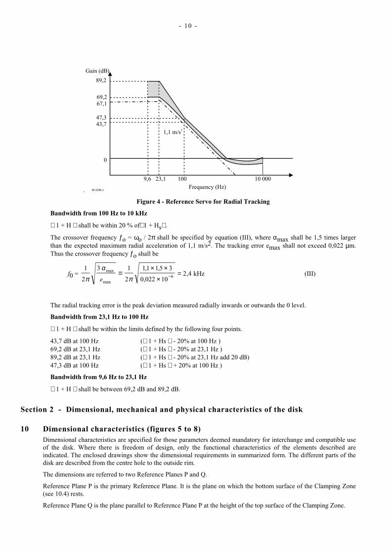
- 10 -
.
Figure 4 - Reference Servo for Radial Tracking
Bandwidth from 100 Hz to 10 kHz
1 + H shall be within 20 % of 1 + Hs .
The crossover frequency ƒo = ωo / 2π shall be specified by equation (III), where αmax shall be 1,5 times larger than the expected maximum radial acceleration of 1,1 m/s2. The tracking error emax shall not exceed 0,022 µm. Thus the crossover frequency ƒo shall be
f0 = 1
2
3 1
2
11 1 5 3
0,022 1026π
α
πmax
max
, ,,4
e=
× ×
×=− kHz (III)
The radial tracking error is the peak deviation measured radially inwards or outwards the 0 level.
Bandwidth from 23,1 Hz to 100 Hz
1 + H shall be within the limits defined by the following four points.
43,7 dB at 100 Hz ( 1 + Hs - 20% at 100 Hz ) 69,2 dB at 23,1 Hz ( 1 + Hs - 20% at 23,1 Hz ) 89,2 dB at 23,1 Hz ( 1 + Hs - 20% at 23,1 Hz add 20 dB) 47,3 dB at 100 Hz ( 1 + Hs + 20% at 100 Hz )
Bandwidth from 9,6 Hz to 23,1 Hz
1 + H shall be between 69,2 dB and 89,2 dB.
Section 2 - Dimensional, mechanical and physical characteristics of the disk
10 Dimensional characteristics (figures 5 to 8) Dimensional characteristics are specified for those parameters deemed mandatory for interchange and compatible use of the disk. Where there is freedom of design, only the functional characteristics of the elements described are indicated. The enclosed drawings show the dimensional requirements in summarized form. The different parts of the disk are described from the centre hole to the outside rim.
The dimensions are referred to two Reference Planes P and Q.
Reference Plane P is the primary Reference Plane. It is the plane on which the bottom surface of the Clamping Zone (see 10.4) rests.
Reference Plane Q is the plane parallel to Reference Plane P at the height of the top surface of the Clamping Zone.

- 11 -
10.1 Overall dimensions The disk shall have an overall diameter
d1 = 120,00 mm ± 0,30 mm
The centre hole of a substrate or a dummy substrate shall have a diameter
+ 0,15 mm d2 = 15,00 mm - 0,00 mm
The diameter of the hole of an assembled disk, i.e. with both parts bonded together, shall be 15,00 mm min., see figure 6.
There shall be no burr on both edges of the centre hole.
The edge of the centre hole shall be rounded off or chamfered. The rounding radius shall be 0,1 mm max. The chamfer shall extend over a height of 0,1 mm max.
The thickness of the disk, including adhesive layer, spacer(s) and label(s), shall be
+ 0,30 mm e1 = 1,20 mm - 0,06 mm
10.2 First transition area In the area defined by d2 and
d3 = 16,0 mm min.
the surface of the disk is permitted to be above Reference Plane P and/or below Reference Plane Q by 0,10 mm max.
10.3 Second transition area This area shall extend between diameter d3 and diameter
d4 = 22,0 mm max.
In this area the disk may have an uneven surface or burrs up to 0,05 mm max. beyond Reference Planes P and/or Q.
10.4 Clamping Zone This zone shall extend between diameter d4 and diameter
d5 = 33,0 mm min.
Each side of the Clamping Zone shall be flat within 0,1 mm. The top side of the Clamping Zone, i.e. that of Reference Plane Q shall be parallel to the bottom side, i.e. that of Reference Plane P within 0,1 mm.
In the Clamping Zone the thickness e2 of the disk shall be
+ 0,20 mm e2 = 1,20 mm - 0,10 mm
10.5 Third transition area This area shall extend between diameter d5 and diameter
d6 = 44,0 mm max.
In this area the top surface is permitted to be above Reference Plane Q by
h1 = 0,25 mm max.
or below Reference Plane Q by
h2 = 0,10 mm max.
The bottom surface is permitted to be above Reference Plane P by
h3 = 0,10 mm max

- 12 -
or below Reference Plane P by
h4 = 0,25 mm max.
10.6 Information Zone The Information Zone shall extend from the beginning of the Lead-in Zone to diameter d10 the value of which is specified in table 1.
In the Information Zone the thickness of the disk shall be equal to e1 specified in 10.1.
10.6.1 Sub-divisions of the Information Zone
The main parts of the Information Zone are
− the Lead-in Zone − the Data Zone − the Lead-out Zone
The area extending from d6 to diameter
d7 = 45,2 mm max.
shall be used as follows
− it is the beginning of the Lead-in Zone for Types A and B, and each pair of layers for Type C and D in PTP mode and on Layer 0 in OTP mode,
− it is the end of the Lead-out Zone on Layer 1 for Types C and D in OTP mode.
In the first case, the Lead-in Zone shall end at diameter
+ 0,0 mm d8 = 48,0 mm
- 0,4 mm
which is the beginning of the Data Zone.
In the second case the Data Zone shall not extend toward the centre of the disk beyond d8. The Lead-out Zone shall start after the Data Zone and end between diameters d6 and d7.
The Data Zone shall start after the Lead-in Zone at diameter d8, it shall extend up to diameter
d9 = 116,0 mm max.
The zone between diameters d9 and d10 constitutes the Lead-out Zone in the cases Types A and B, and Types C and D in PTP mode and the Middle Zone in the case of Types C and D in OTP mode.
The Lead-out Zone in PTP mode and the Middle Zone shall start after the Data Zone and end at diameter d10 the value of which depends on the length of the Data Zone as shown in table 1.
Table 1 - End of the Information Zone
Length of the Data Zone Value of diameter d10
Less than 68,0 mm 70,0 mm min.
68,0 mm to 115,0 mm Data Zone diameter + 2,0 mm min.
115,0 mm to 116,0 mm 117,0 mm min.
The zone extending from d11 to d12 shall be used for the Burst Cutting Area, if implemented (see annex H).
10.6.2 Track geometry
In the Information Zone tracks are constituted by a 360° turn of a spiral.
The track pitch shall be 0,74 µm ± 0,03 µm.
The track pitch averaged over the Data Zone shall be 0,74 µm ± 0,01 µm.

- 13 -
10.6.3 Track modes
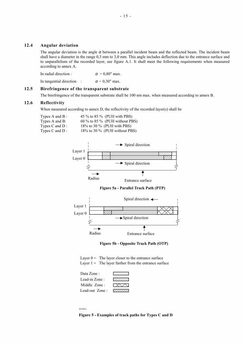
Tracks can be recorded in two different modes called Parallel Track Path (PTP) and Opposite Track Path (OTP). Figure 5 shows examples of the PTP and OTP modes. In practice, the lengths of the Data Zones of both layers are independent from each other.
Types A and B shall be recorded in PTP mode only.
Types C and D may be recorded in either modes.
In PTP mode, tracks are read from the inside diameter of the Information Zone to its outside diameter, this applies to both Layer 0 and Layer 1 for Types C and D, see figure 5a. On both layers, the track spiral is turning from the inside to the outside.
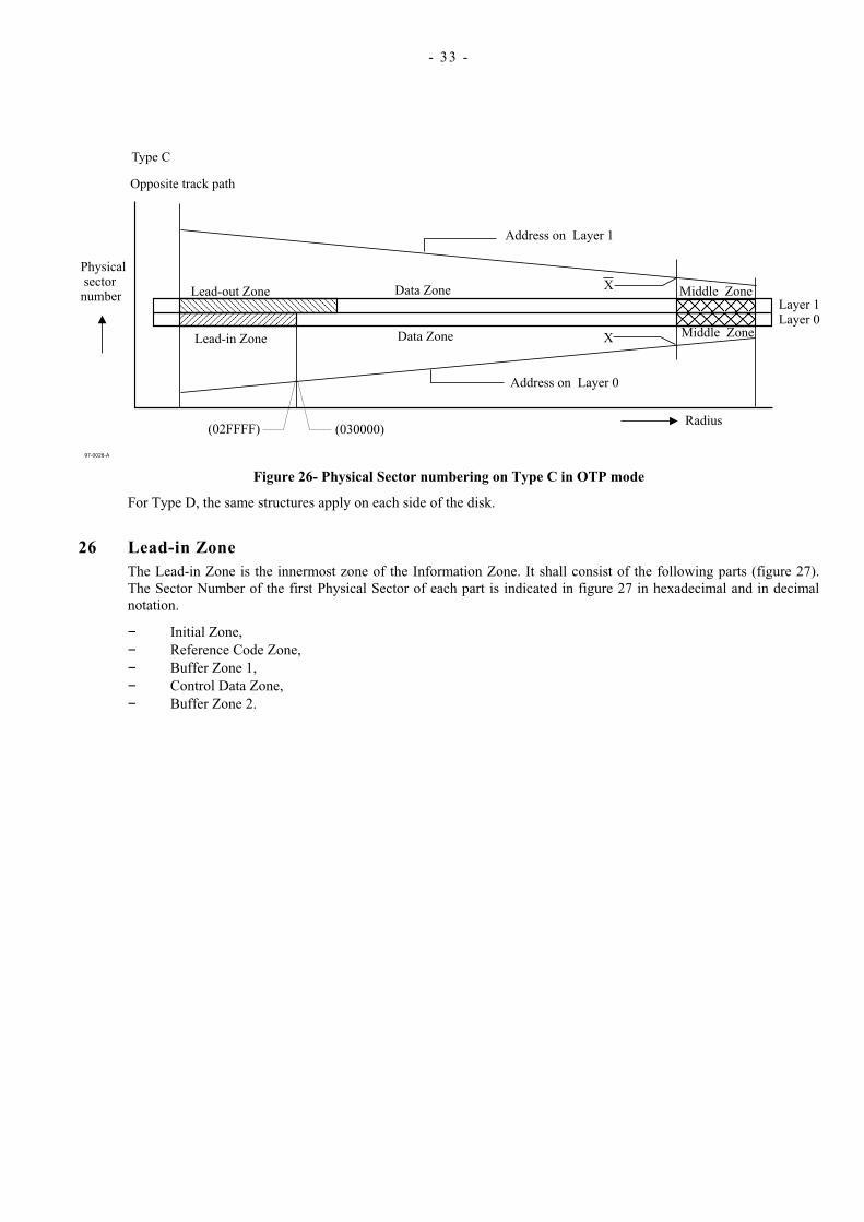
In OTP mode, tracks are read starting on Layer 0 at the inner diameter of the Information Zone, continuing on Layer 1 from the outer diameter to the inner diameter. Thus, there is a Middle Zone at the outer diameter on both layers, see figure 5b. The track spiral is turning from the inside to the outside on Layer 0 and in the reverse direction on Layer 1.
The radial misalignment of the outer edge of the Information Zones between Layer 0 and Layer 1 shall be 0,5 mm max.
In OTP mode, the radial misalignment between the outer edge of the Data Zones of Layer 0 and Layer 1 shall be 0,5 mm max.
10.6.4 Channel bit length
The Information Zone shall be recorded in CLV mode. The Channel bit length averaged over the Data Zone shall be
− 133,3 nm ± 1,4 nm for Type A and Type B,
− 146,7 nm ± 1,5 nm for Type C and Type D
10.7 Rim area The rim area shall be that area extending from diameter d10 to diameter d1 (see figure 8). In this area the top surface is permitted to be above Reference Plane Q by
h5 = 0,1 mm max.
and the bottom surface is permitted to be below Reference Plane P by
h6 = 0,1 mm max.
The total thickness of this area shall not be greater than 1,50 mm, i.e. the maximum value of e1. The thickness of the rim proper shall be
e3 = 0,6 mm min.
The outer edges of the disk shall be either rounded off with a rounding radius of 0,2 mm max. or be chamfered over
h7 = 0,2 mm max.
h8 = 0,2 mm max.
10.8 Remark on tolerances All heights specified in the preceding clauses and indicated by hi are independent from each other. This means that, for example, if the top surface of the third transition area is below Reference Plane Q by up to h2, there is no implication that the bottom surface of this area has to be above Reference Plane P by up to h3. Where dimensions have the same - generally maximum - numerical value, this does not imply that the actual values have to be identical.

- 14 -
10.9 Runout 10.9.1 Axial runout
When measured by the PUH with the Reference Servo for axial tracking, the disk rotating at the scanning velocity, the deviation of the recorded layer from its nominal position in the direction normal to the Reference Planes shall not exceed 0,3 mm.
The residual tracking error below 10 kHz, measured using the Reference Servo for axial tracking, shall be less than 0,23 µm. The measuring filter shall be a Butterworth LPF, ƒc (-3dB): 10 kHz, slope : -80 dB/decade.
10.9.2 Radial runout
The runout of the outer edge of the disk shall be less than 0,3 mm, peak-to-peak.
The radial runout of tracks shall be less than 100 µm, peak-to-peak.
The residual tracking error below 1,1 kHz, measured using the Reference Servo for radial tracking, shall be less than 0,022 µm. The measuring filter shall be a Butterworth LPF, ƒc (-3dB) : 1,1 kHz, slope : -80 dB/decade.
The rms noise value of the residual error signal in the frequency band from 1,1 kHz to 10 kHz, measured with an integration time of 20 ms, using the Reference Servo for radial tracking, shall be less than 0,016 µm. The measuring filter shall be a Butterworth BPF, frequency range (-3dB) : 1,1 kHz, slope : +80 dB/decade to 10 kHz, slope : -80 dB/decade.
10.10 Label The label shall be placed on the side of the disk opposite the entrance surface for the information to which the label is related. The label shall be placed either on an outer surface of the disk or inside the disk bonding plane. In the former case, the label shall not extend over the Clamping Zone. In the latter case, the label may extend over the Clamping Zone. In both cases, the label shall not extend over the rim of the centre hole nor over the outer edge of the disk.
11 Mechanical parameters 11.1 Mass
The mass of the disk shall be in the range 13 g to 20 g.
11.2 Moment of inertia
The moment of inertia of the disk, relative to its rotation axis, shall not exceed 0,040 g•m2.
11.3 Dynamic imbalance
The dynamic imbalance of the disk, relative to its rotation axis, shall not exceed 0,010 g•m.
11.4 Sense of rotation The sense of rotation of the disk shall be counterclockwise as seen by the optical system.
12 Optical parameters 12.1 Index of refraction
The index of refraction IR of the transparent substrate shall be 1,55 ± 0,10.
The index of refraction of the spacer shall be (IR ± 0,10).
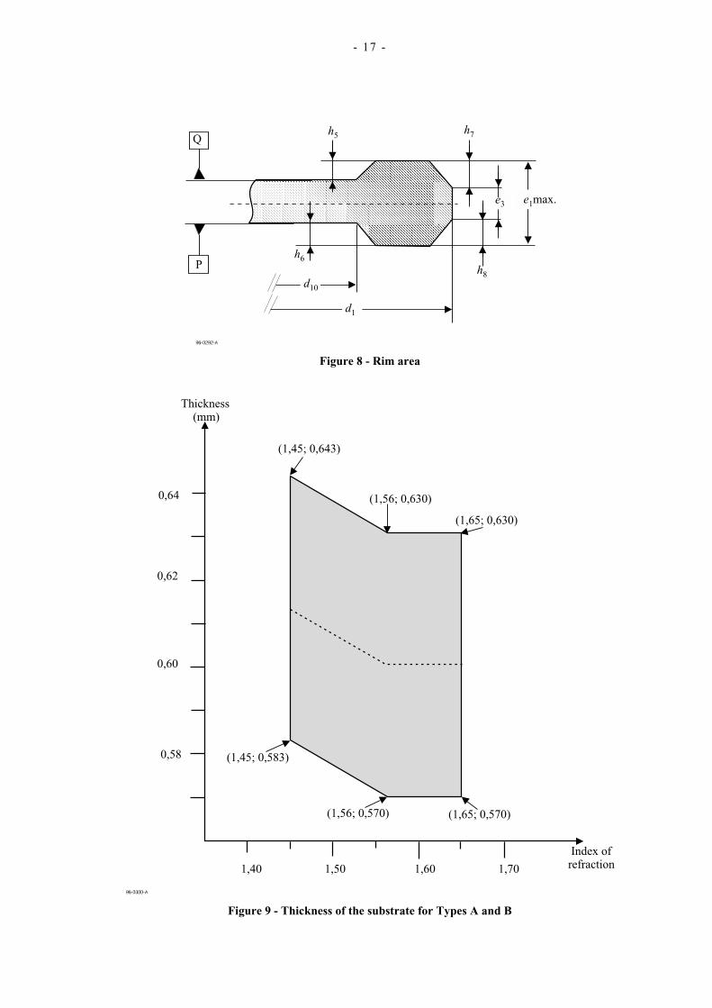
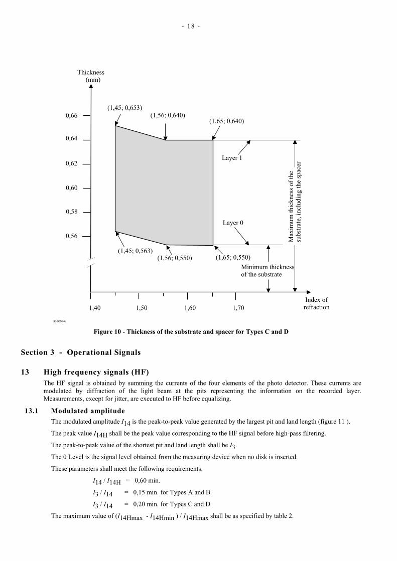
12.2 Thickness of the transparent substrate The thickness of the transparent substrate is specified as a function of its index of refraction.
Figure 9 specifies it for Types A and B and figure 10 for Types C and D.
12.3 Thickness of the spacer of Types C and D
For Types C and D, the thickness of the spacer shall be 55 µm ± 15 µm. Annex K shows two ways of measuring this thickness. On a disk, this thickness shall not vary by more than 20 µm. Within one revolution, it shall not vary by more than 8 µm.
- 15 -
12.4 Angular deviation
The angular deviation is the angle α between a parallel incident beam and the reflected beam. The incident beam shall have a diameter in the range 0,3 mm to 3,0 mm. This angle includes deflection due to the entrance surface and to unparallelism of the recorded layer, see figure A.1. It shall meet the following requirements when measured according to annex A.
In radial direction : α = 0,80° max.
In tangential direction : α = 0,30° max.
12.5 Birefringence of the transparent substrate The birefringence of the transparent substrate shall be 100 nm max. when measured according to annex B.
12.6 Reflectivity When measured according to annex D, the reflectivity of the recorded layer(s) shall be
Types A and B : 45 % to 85 % (PUH with PBS) Types A and B: 60 % to 85 % (PUH without PBS) Types C and D : 18% to 30 % (PUH with PBS) Types C and D : 18% to 30 % (PUH without PBS)
Figure 5 - Examples of track paths for Types C and D

- 16 -
Figure 6- Hole of the assembled disk
Figure 7 - Areas of the disk
- 17 -
Figure 8 - Rim area
Figure 9 - Thickness of the substrate for Types A and B
- 18 -
Figure 10 - Thickness of the substrate and spacer for Types C and D
Section 3 - Operational Signals
13 High frequency signals (HF) The HF signal is obtained by summing the currents of the four elements of the photo detector. These currents are modulated by diffraction of the light beam at the pits representing the information on the recorded layer. Measurements, except for jitter, are executed to HF before equalizing.
13.1 Modulated amplitude The modulated amplitude I14 is the peak-to-peak value generated by the largest pit and land length (figure 11 ).
The peak value I14H shall be the peak value corresponding to the HF signal before high-pass filtering.
The peak-to-peak value of the shortest pit and land length shall be I3.
The 0 Level is the signal level obtained from the measuring device when no disk is inserted.
These parameters shall meet the following requirements.
I14 / I14H = 0,60 min.
I3 / I14 = 0,15 min. for Types A and B
I3 / I14 = 0,20 min. for Types C and D
The maximum value of (I14Hmax - I14Hmin ) / I14Hmax shall be as specified by table 2.

- 19 -
Table 2 - Maximum value of (I14Hmax - I14Hmin ) / I14Hmax
Within one recorded side of a disk
Within one revolution
PUH with PBS 0,33 0,15
PUH without PBS with circular polarization
0,20 0,10
13.2 Signal asymmetry The signal asymmetry shall meet the following requirement, see figure 11.
- 0,05 ≤ [ (I14H + I14L) / 2 - (I3H + I3L) / 2 ] / I14 ≤ 0,15
where
− (I14H + I14L) / 2 is the centre level of I14
− (I3H + I3L) / 2 is the centre level of I3.
13.3 Cross-track signal The cross-track signal shall be derived from the HF signal when low-pass filtered with a cut-off frequency of 30 kHz when the light beam crosses the tracks (see figure 12). The low-pass filter is a 1st order filter. The cross-track signal shall meet the following requirements.
IT = IH - IL
IT / IH = 0,10 min.
where IH is the peak value of this signal and IT is the peak-to-peak value.
13.4 Quality of signals 13.4.1 Jitter
Jitter is the standard deviation σ of the time variation of the digitized data passed through the equalizer. The jitter of the leading and trailing edges is measured to the PLL clock and normalized by the Channel bit clock period.
Jitter shall be less than 8,0 % of the Channel bit clock period, when measured according to annex F.
13.4.2 Random errors
A row of an ECC Block (see clause 18) that has at least 1 byte in error constitutes a PI error. In any 8 consecutive ECC Blocks the total number of PI errors before correction shall not exceed 280.
13.4.3 Defects
Defect are air bubbles and black spots. Their diameter shall meet the following requirements
− for air bubbles it shall not exceed 100 µm,
− for black spots causing birefringence it shall not exceed 200 µm,
− for black spots not causing birefringence it shall not exceed 300 µm.
In addition, over a distance of 80 mm in scanning direction of tracks, the following requirements shall be met
− the total length of defects larger than 30 µm shall not exceed 300 µm,
− there shall be at most 6 such defects.
14 Servo signals The output currents of the four quadrants of the split photo detector shown in figure 13 are identified by Ia, Ib, Ic and Id.
- 20 -
14.1 Differential phase tracking error signal The differential phase tracking error signal shall be derived from the phase difference between diagonal pairs of detectors elements when the light beam crosses the tracks : Phase (Ia + Ic) - Phase (Ib + Id) , see figure 13. The differential phase tracking error signal shall be low-pass filtered with a cut-off frequency of 30 kHz, see annex C. This signal shall meet the following requirements (see figure 14).
Amplitude
At the positive 0 crossing ∆t /T shall be in the range 0,5 to 1,1 at 0,10 µm radial offset, where ∆t is the average time difference derived from the phase difference between diagonal pairs of detector elements, and T is the Channel bit clock period .
Asymmetry (figure 14)
The asymmetry shall meet the following requirement.
T T
T T
1 2
1 2
0,2−
+≤
where
− T1 is the positive peak value of ∆t / T
− T2 is the negative peak value of ∆t / T
14.2 Tangential push-pull signal This signal shall be derived from the instantaneous level of the differential output (Ia + Id) - (Ib + Ic). It shall meet the following requirement, see figure15.
0 ≤ ( ) ( )[ ]I I I I
I
a d b c pp+ − +
≤14
0,9
97 -0 002 -A
0 L ev e l
I
I
I
I
I1 4
1 4 L
3 L
3 H
1 4 HI 3
Figure 11 - Modulated amplitude
- 21 -
Figure 12 - Cross-track signal
Figure 13 - Quadrant photo detector
Figure 14 - Differential phase tracking error signal
- 22 -
( + ) ( ) I I I Ia d b c
− +
P it
97-0004-A
p p
Figure 15 - Tangential push-pull signal
Section 4 - Data Format
15 General The data received from the host, called Main Data, is formatted in a number of steps before being recorded on the disk. It is transformed successively into
− a Data Frame, − a Scrambled Frame, − an ECC Block, − a Recording Frame, − a Physical Sector
These steps are specified in the following clauses.
16 Data Frames (figure 16) A Data Frame shall consist of 2 064 bytes arranged in an array of 12 rows each containing 172 bytes (figure 16). The first row shall start with three fields, called Identification Data (ID), the check bytes of the ID Error Detection Code (IED), and Copyright Management Information (CPR_MAI), followed by 160 Main Data bytes. The next 10 rows shall each contain 172 Main Data bytes, and the last row shall contain 168 Main Data bytes followed by four bytes for recording the check bits of an Error Detection Code (EDC). The 2 048 Main Data bytes are identified as D0 to D2 047.
- 23 -
Figure 16 - Data Frame
16.1 Identification Data (ID) This field shall consist of four bytes the bits of which are numbered consecutively from b0 (lsb) to b31 (msb), see figure 17.
b31 b24 b23 b0
Sector Information Sector Number
Figure 17 - Identification Data (ID)
b31 b30 b29 b28 b27 and b26 b25 b24
Sector Format type
Tracking method
Reflectivity Reserved Zone type Data type Layer number
Figure 18 - Sector Information of the Identification Data (ID)
The least significant three bytes, bits b0 to b23, shall specify the sector number in binary notation. The sector number of the first sector of an ECC Block of 16 sectors shall be a multiple of 16.
The bits of the most significant byte, the Sector Information, shall be set as follows.
Bit b24 shall be set to
ZERO on Layer 0 of DL disks ONE on Layer 1 of DL disks ZERO on SL disks
Bit b25 shall be set to ZERO, indicating read-only data
- 24 -
Bits b26 and b27 shall be set to
ZERO ZERO in the Data Zone ZERO ONE in the Lead-in Zone ONE ZERO in the Lead-out Zone ONE ONE in the Middle Zone
Bit b28 shall be set to ZERO
Bit b29 shall be set to
ZERO if the reflectivity is greater than 40 % with PBS PUH ONE if the reflectivity is 40 % max. with PBS PUH
Bit b30 shall be set to ZERO, indicating pit tracking
Bit b31 shall be set to ZERO, indicating the CLV format for read-only disks
Other setting are prohibited by this ECMA Standard.
16.2 ID Error Detection Code (IED) When identifying all bytes of the array shown in figure 16 as Ci,j for i = 0 to 11 and j = 0 to171, the check bytes of IED are represented by C0,j for j = 4 to 5. Their setting is obtained as follows.
IED(x) = j=∑
4
5
C0,j x5-j = I(x) x2 mod GE(x)
where
3
I(x) =∑∑∑∑ C0,j x3-j
j=0
1
GE(x) = ΠΠΠΠ ( x + αk ) k=0
α is the primitive root of the primitive polynomial P(x) = x8 + x4 + x3 + x2 + 1
16.3 Copyright Management Information (CPR_MAI) This field shall consist of 6 bytes. Their setting is application-dependent, for instance a video application. If this setting is not specified by the application, the default setting shall be to set all bytes to all ZEROs.
16.4 Error Detection Code (EDC) This 4-byte field shall contain the check bits of an Error Detection Code computed over the preceding 2 060 bytes of the Data Frame. Considering the Data Frame as a single bit field starting with the most significant bit of the first byte of the ID field and ending with the least significant bit of the EDC field, then this msb will be b16 511 and the lsb will be b0. Each bit bi of the EDC is as follows for i = 31 to 0 :
0
EDC(x) = ∑∑∑∑ bi xi = I(x) mod G(x)
i=31
where
32
I(x) = ∑∑∑∑ bi xi
i=16 511
G(x) = x32 + x31 + x4 + 1
- 25 -
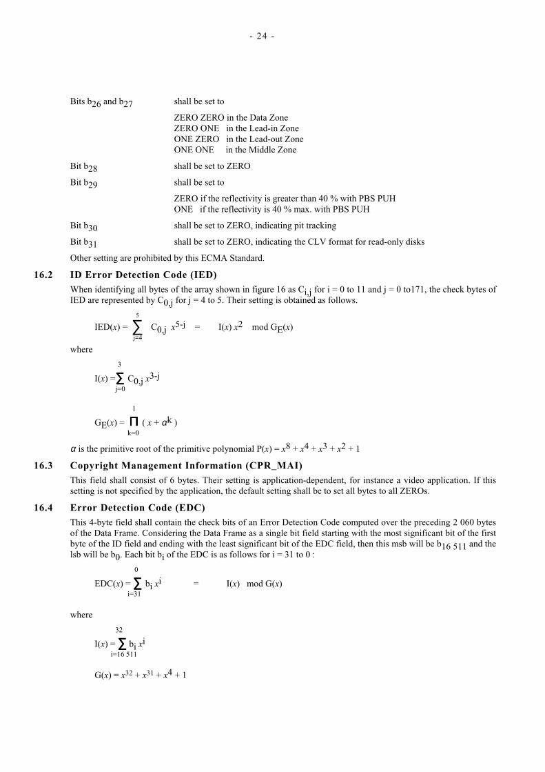
17 Scrambled Frames The 2 048 Main Data bytes shall be scrambled by means of the circuit shown in figure 19 which shall consist of a feedback bit shift register in which bits r7 (msb) to r0 (lsb) represent a scrambling byte at each 8-bit shift. At the beginning of the scrambling procedure of a Data Frame, positions r14 to r0 shall be pre-set to the value(s) specified in table 3. The same pre-set value shall be used for 16 consecutive Data Frames. After 16 groups of 16 Data Frames, the sequence is repeated. The initial pre-set number is equal to the value represented by bits b7 (msb) to bit b4 (lsb) of the ID field of the Data Frame. Table 3 specifies the initial pre-set value of the shift register corresponding to the 16 initial pre-set numbers.
Table 3 - Initial values of the shift register
Initial pre-set number
Initial pre-set value
Initial pre-set number
Initial pre-set value
(0) (0001) (8) (0010)
(1) (5500) (9) (5000)
(2) (0002) (A) (0020)
(3) (2A00) (B) (2001)
(4) (0004) (C) (0040)
(5) (5400) (D) (4002)
(6) (0008) (E) (0080)
(7) (2800) (F) (0005)
Figure 19 - Feedback shift register
The part of the initial value of r7 to r0 is taken out as scrambling byte S0. After that, 8-bit shift is repeated 2 047 times and the following 2 047 bytes shall be taken from r7 to r0 as scrambling bytes S1 to S2 047. The Main Data bytes Dk of the Data Frame become scrambled bytes D’k where
D’k = Dk ⊕ Sk for k = 0 to 2 047
⊕ stands for Exclusive OR
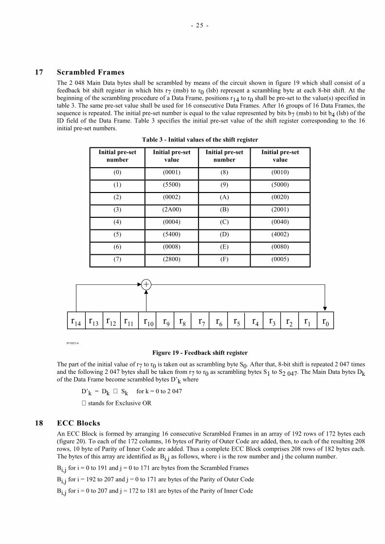
18 ECC Blocks An ECC Block is formed by arranging 16 consecutive Scrambled Frames in an array of 192 rows of 172 bytes each (figure 20). To each of the 172 columns, 16 bytes of Parity of Outer Code are added, then, to each of the resulting 208 rows, 10 byte of Parity of Inner Code are added. Thus a complete ECC Block comprises 208 rows of 182 bytes each. The bytes of this array are identified as Bi,j as follows, where i is the row number and j the column number.
Bi,j for i = 0 to 191 and j = 0 to 171 are bytes from the Scrambled Frames
Bi,j for i = 192 to 207 and j = 0 to 171 are bytes of the Parity of Outer Code
Bi,j for i = 0 to 207 and j = 172 to 181 are bytes of the Parity of Inner Code
- 26 -
97-0022-A
1 7 2 b y te s P I 1 0 b y te s
1 9 2 ro w s
B
B
B
B
B
B B B B B
B B B B
B B B B
B
B
B
B
B
B
B
B
B
B
B B B
B B
B B B
B B B
B B B
B
B
B
B
B
P O 1 6 row s
0 ,0 0 ,1 7 0 0 ,1 7 1
1 ,1 7 1
2 ,1 7 1
1 ,1 7 0
2 ,1 7 0
1 ,0
2 ,0
0 ,1
1 ,1
2 ,1
0 ,1 7 2 0 ,1 8 1
1 8 9 ,0 1 8 9 ,1 1 8 9 ,1 7 0 1 8 9 ,1 7 1 1 8 9 ,1 7 2 1 8 9 ,1 8 1
1 9 0 ,1 1 9 0 ,1 7 0 1 9 0 ,1 7 1 1 9 0 ,1 7 2 1 9 0 ,1 8 1
1 9 1 ,1 1 9 1 ,1 7 0 1 9 1 ,1 7 1 1 9 1 ,1 7 2 1 9 1 ,1 8 1
1 9 2 ,1 1 9 2 ,1 7 0 1 9 2 ,1 7 1 1 9 2 ,1 7 2 1 9 2 ,1 8 1
1 9 0 ,0
1 9 1 ,0
1 9 2 ,0
1 ,1 7 2 1 ,1 8 1
2 ,1 7 2 2 ,1 8 1
2 0 7 ,0 2 0 7 ,1 2 0 7 ,1 7 0 2 0 7 ,1 7 1 2 0 7 ,1 7 2 2 0 7 ,1 8 1
B
Figure 20 - ECC Block
The PO and PI bytes shall be obtained as follows.
In each of columns j = 0 to 171, the 16 PO bytes are defined by the remainder polynomial Rj(x) to form the outer code RS (208,192,17).
207
Rj(x) = ∑∑∑∑ Bi,j x207-i = Ij(x) x16 mod GPO(x)
i=192
where
191
Ij(x) = ∑∑∑∑ Bi,j x191-i
i=0
15
GPO(x) = ΠΠΠΠ (x + αk ) k=0
In each of rows i = 0 to 207, the 10 PI bytes are defined by the remainder polynomial Ri(x) to form the inner code RS (182,172,11).
181
Ri(x) = ∑∑∑∑ Bi,j x181-j = Ii(x) x10 mod GPI(x)
j=172

- 27 -
where
171
Ii(x) = ∑∑∑∑ Bi,j x171-j
j=0
9
GPI(x) = ΠΠΠΠ (x + αk ) k=0
α is the primitive root of the primitive polynomial P(x) = x8 + x4 + x3 + x2 + 1
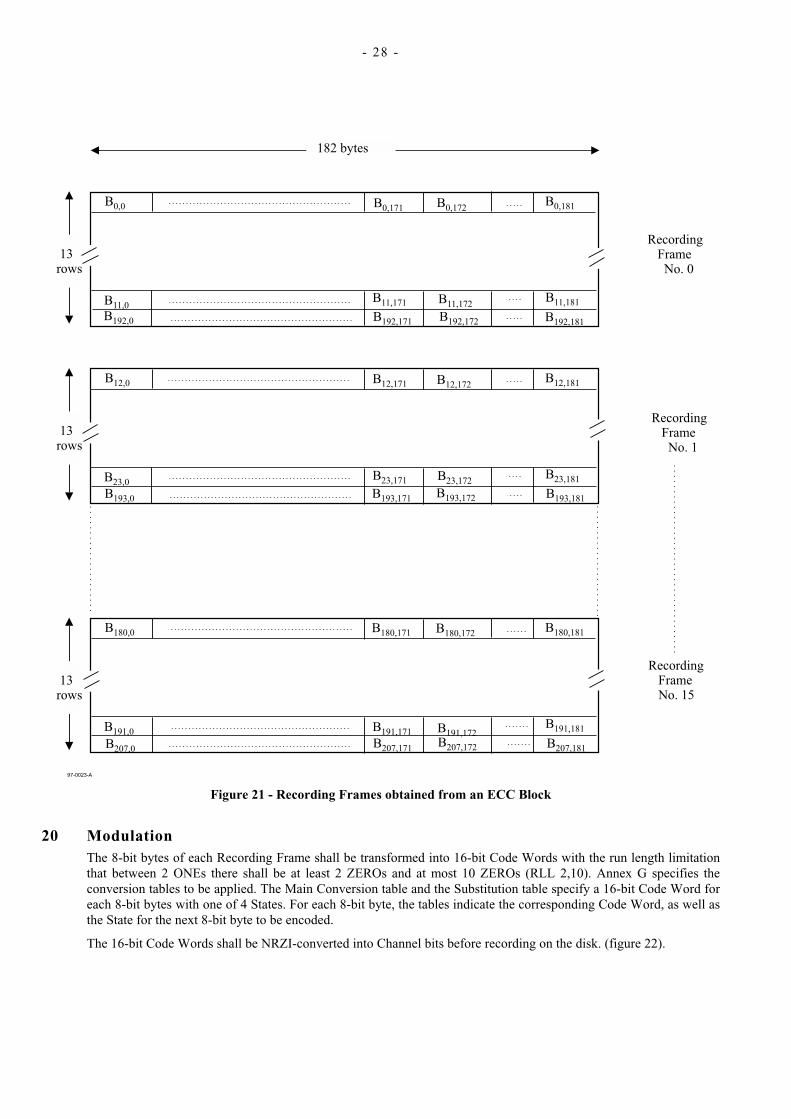
19 Recording Frames Sixteen Recording Frames shall be obtained by interleaving one of the 16 PO rows at a time after every 12 rows of an ECC Block (figure 21). This is achieved by re-locating the bytes Bi,j of the ECC Block as Bm,n for
m = i + int[i / 12] and n = j for i ≤ 191
m = 13 (i - 191) - 1 and n = j for i ≥ 192
where int[x] represents the largest integer not greater than x.
Thus the 37 856 bytes of an ECC Block are re-arranged into 16 Recording Frames of 2 366 bytes. Each Recording Frame consists of an array of 13 rows of 182 bytes.
- 28 -
Figure 21 - Recording Frames obtained from an ECC Block
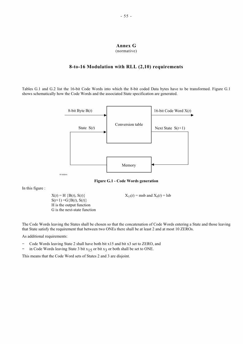
20 Modulation The 8-bit bytes of each Recording Frame shall be transformed into 16-bit Code Words with the run length limitation that between 2 ONEs there shall be at least 2 ZEROs and at most 10 ZEROs (RLL 2,10). Annex G specifies the conversion tables to be applied. The Main Conversion table and the Substitution table specify a 16-bit Code Word for each 8-bit bytes with one of 4 States. For each 8-bit byte, the tables indicate the corresponding Code Word, as well as the State for the next 8-bit byte to be encoded.
The 16-bit Code Words shall be NRZI-converted into Channel bits before recording on the disk. (figure 22).
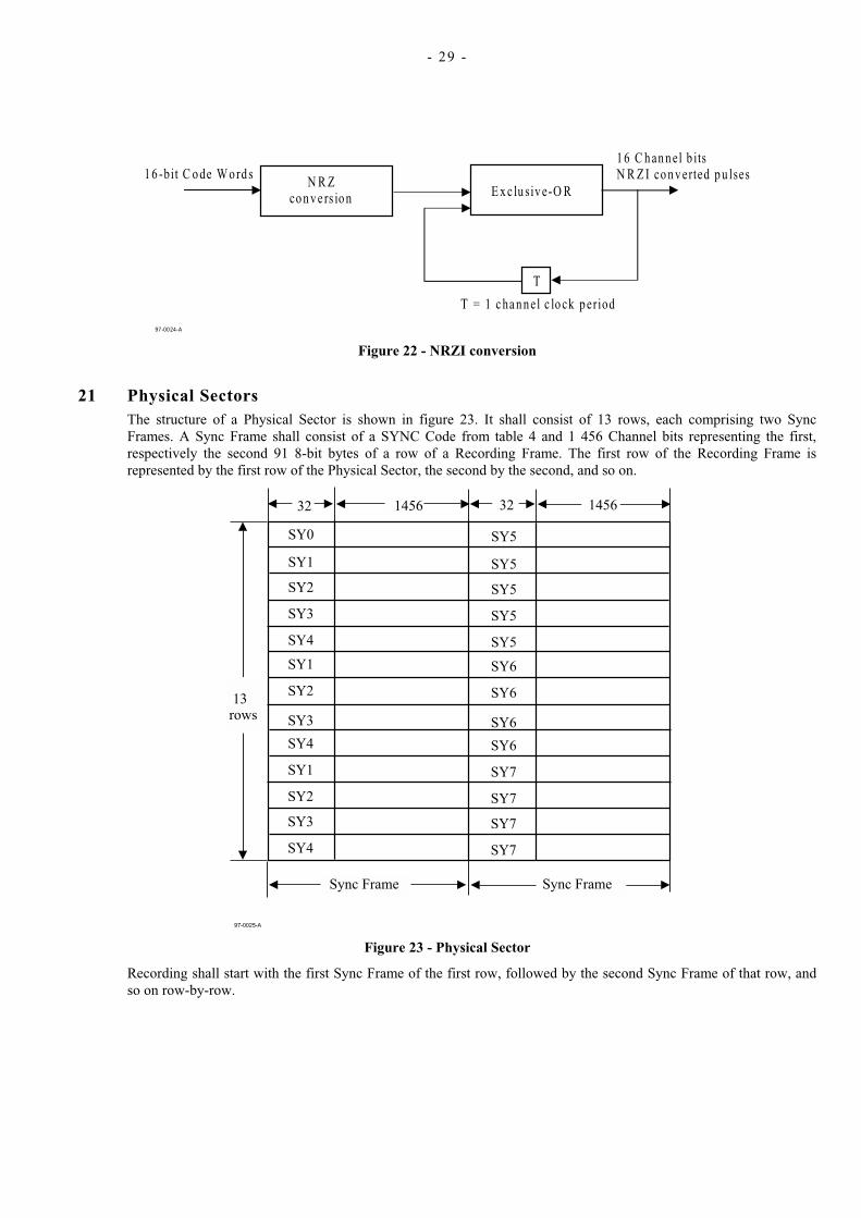
- 29 -
97-0024-A
1 6 -bit C o de W o rd s N R Zco n v e rs io n E x c lu siv e-O R
1 6 C h an n el b its N R Z I co n v erted p u lses
T = 1 c ha n n el c lo ck p eriod
T
Figure 22 - NRZI conversion
21 Physical Sectors The structure of a Physical Sector is shown in figure 23. It shall consist of 13 rows, each comprising two Sync Frames. A Sync Frame shall consist of a SYNC Code from table 4 and 1 456 Channel bits representing the first, respectively the second 91 8-bit bytes of a row of a Recording Frame. The first row of the Recording Frame is represented by the first row of the Physical Sector, the second by the second, and so on.
Figure 23 - Physical Sector
Recording shall start with the first Sync Frame of the first row, followed by the second Sync Frame of that row, and so on row-by-row.
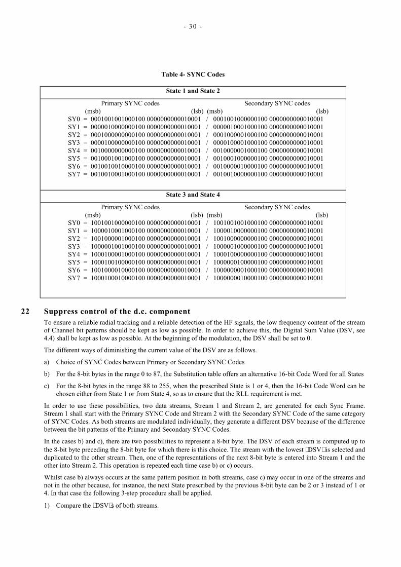
- 30 -
Table 4- SYNC Codes
State 1 and State 2
Primary SYNC codes Secondary SYNC codes (msb) (lsb) (msb) (lsb) SY0 = 0001001001000100 0000000000010001 / 0001001000000100 0000000000010001 SY1 = 0000010000000100 0000000000010001 / 0000010001000100 0000000000010001 SY2 = 0001000000000100 0000000000010001 / 0001000001000100 0000000000010001 SY3 = 0000100000000100 0000000000010001 / 0000100001000100 0000000000010001 SY4 = 0010000000000100 0000000000010001 / 0010000001000100 0000000000010001 SY5 = 0010001001000100 0000000000010001 / 0010001000000100 0000000000010001 SY6 = 0010010010000100 0000000000010001 / 0010000010000100 0000000000010001 SY7 = 0010010001000100 0000000000010001 / 0010010000000100 0000000000010001
State 3 and State 4
Primary SYNC codes Secondary SYNC codes (msb) (lsb) (msb) (lsb) SY0 = 1001001000000100 0000000000010001 / 1001001001000100 0000000000010001 SY1 = 1000010001000100 0000000000010001 / 1000010000000100 0000000000010001 SY2 = 1001000001000100 0000000000010001 / 1001000000000100 0000000000010001 SY3 = 1000001001000100 0000000000010001 / 1000001000000100 0000000000010001 SY4 = 1000100001000100 0000000000010001 / 1000100000000100 0000000000010001 SY5 = 1000100100000100 0000000000010001 / 1000000100000100 0000000000010001 SY6 = 1001000010000100 0000000000010001 / 1000000001000100 0000000000010001 SY7 = 1000100010000100 0000000000010001 / 1000000010000100 0000000000010001
22 Suppress control of the d.c. component To ensure a reliable radial tracking and a reliable detection of the HF signals, the low frequency content of the stream of Channel bit patterns should be kept as low as possible. In order to achieve this, the Digital Sum Value (DSV, see 4.4) shall be kept as low as possible. At the beginning of the modulation, the DSV shall be set to 0.
The different ways of diminishing the current value of the DSV are as follows.
a) Choice of SYNC Codes between Primary or Secondary SYNC Codes
b) For the 8-bit bytes in the range 0 to 87, the Substitution table offers an alternative 16-bit Code Word for all States
c) For the 8-bit bytes in the range 88 to 255, when the prescribed State is 1 or 4, then the 16-bit Code Word can be chosen either from State 1 or from State 4, so as to ensure that the RLL requirement is met.
In order to use these possibilities, two data streams, Stream 1 and Stream 2, are generated for each Sync Frame. Stream 1 shall start with the Primary SYNC Code and Stream 2 with the Secondary SYNC Code of the same category of SYNC Codes. As both streams are modulated individually, they generate a different DSV because of the difference between the bit patterns of the Primary and Secondary SYNC Codes.
In the cases b) and c), there are two possibilities to represent a 8-bit byte. The DSV of each stream is computed up to the 8-bit byte preceding the 8-bit byte for which there is this choice. The stream with the lowest DSV is selected and duplicated to the other stream. Then, one of the representations of the next 8-bit byte is entered into Stream 1 and the other into Stream 2. This operation is repeated each time case b) or c) occurs.
Whilst case b) always occurs at the same pattern position in both streams, case c) may occur in one of the streams and not in the other because, for instance, the next State prescribed by the previous 8-bit byte can be 2 or 3 instead of 1 or 4. In that case the following 3-step procedure shall be applied.
1) Compare the DSV s of both streams.
- 31 -
2) If the DSV of the stream in which case c) occurs is smaller than that of the other stream, then the stream in which case c) has occurred is chosen and duplicated to the other stream. One of the representations of the next 8-bit byte is entered into this stream and the other into the other stream.
3) If the DSV of the stream in which case c) has occurred is larger than that of the other stream, then case c) is ignored and the 8-bit byte is represented according to the prescribed State.
In both cases b) and c), if the DSV s are equal, the decision to choose Stream 1 or Stream 2 is implementation-defined.
The procedure for case a) shall be as follows. At the end of a Sync Frame, whether or not case b) and or case c) have occurred, the DSV of the whole Sync Frame is computed and the stream with the lower DSV is selected. If this DSV is greater than + 63 or smaller than -64, then the SYNC Code at the beginning of the Sync Frame is changed from Primary to Secondary or vice versa. If this yields a smaller DSV , the change is permanent, if the DSV is not smaller, the original SYNC Code is retained.
During the DSV computation, the actual values of the DSV may vary between -1000 and +1000, thus it is recommended that the count range for the DSV be at least from -1 024 to +1 023.
Section 5 Format of the Information Zone(s)
23 General description of an Information Zone The Information Zone shall be divided in three parts : the Lead-in Zone, the Data Zone and the Lead-out Zone. In SL disks and in DL disks in PTP mode there is one Information Zone per layer. In DL disks in OTP mode, there is only one Information Zone extending over two layers. In DL disks in OTP mode, the Information Zone has a Middle Zone in each layer to allow the read-out beam to move from Layer 0 to Layer 1 (see figure 5b). The Data Zone is intended for the recording of Main Data. The Lead-in Zone contains control information. The Lead-out Zone allows for a continuous smooth read-out.
24 Layout of the Information Zone The Information Zone of SL disks and of DL disks in PTP mode shall be sub-divided as shown in table 5. The value of the radii indicated are the nominal values of the first track of the first Physical Sector and that of the last track of the last Physical Sector of a zone.
Table 5 - Layout of the Information Zone
Nominal radius in mm
Sector Number of the first
Physical Sector
Number of Physical Sectors
Lead-in Zone Initial Zone
22,6 max. to 24,0
Reference Code Zone (02F000) 32
Buffer Zone 1 (02F020) 480
Control Data Zone (02F200) 3 072
Buffer Zone 2 (02FE00) 512
Data Zone 24,0 to r1 (030000)
Lead-out Zone r1 to 35,0 min. when
r1< 34,0
r1 to (r1+1,0) when 34,0≤ r1 ≤ 57,5
r1 to 58,5 when 57,5< r1 < 58,0
- 32 -
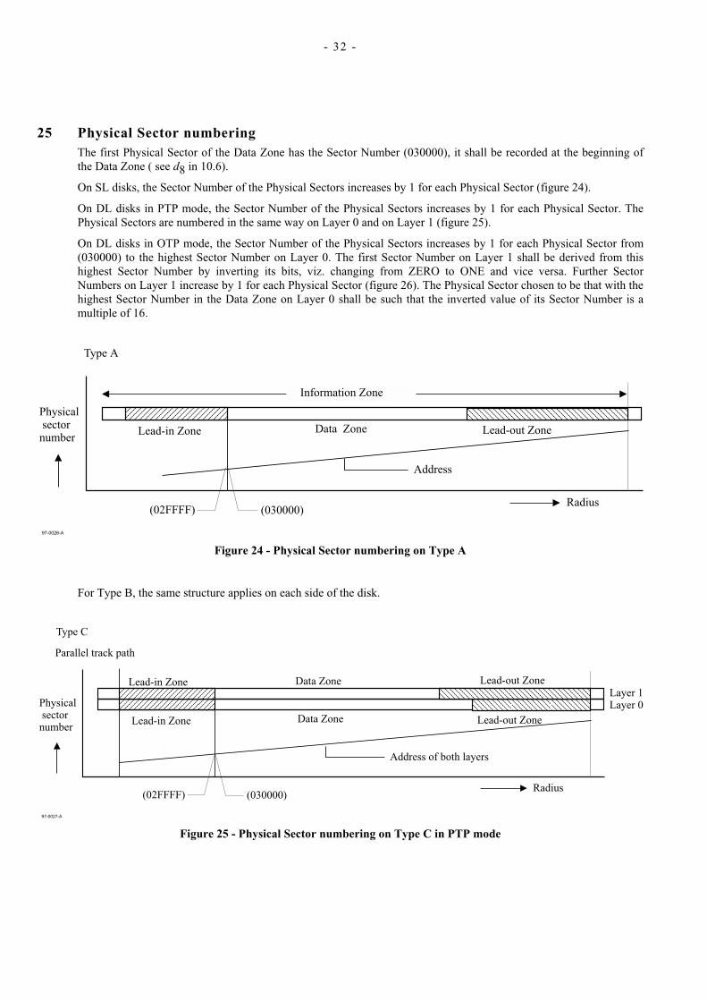
25 Physical Sector numbering The first Physical Sector of the Data Zone has the Sector Number (030000), it shall be recorded at the beginning of the Data Zone ( see d8 in 10.6).
On SL disks, the Sector Number of the Physical Sectors increases by 1 for each Physical Sector (figure 24).
On DL disks in PTP mode, the Sector Number of the Physical Sectors increases by 1 for each Physical Sector. The Physical Sectors are numbered in the same way on Layer 0 and on Layer 1 (figure 25).
On DL disks in OTP mode, the Sector Number of the Physical Sectors increases by 1 for each Physical Sector from (030000) to the highest Sector Number on Layer 0. The first Sector Number on Layer 1 shall be derived from this highest Sector Number by inverting its bits, viz. changing from ZERO to ONE and vice versa. Further Sector Numbers on Layer 1 increase by 1 for each Physical Sector (figure 26). The Physical Sector chosen to be that with the highest Sector Number in the Data Zone on Layer 0 shall be such that the inverted value of its Sector Number is a multiple of 16.
Figure 24 - Physical Sector numbering on Type A
For Type B, the same structure applies on each side of the disk.
Figure 25 - Physical Sector numbering on Type C in PTP mode
- 33 -
Figure 26- Physical Sector numbering on Type C in OTP mode
For Type D, the same structures apply on each side of the disk.
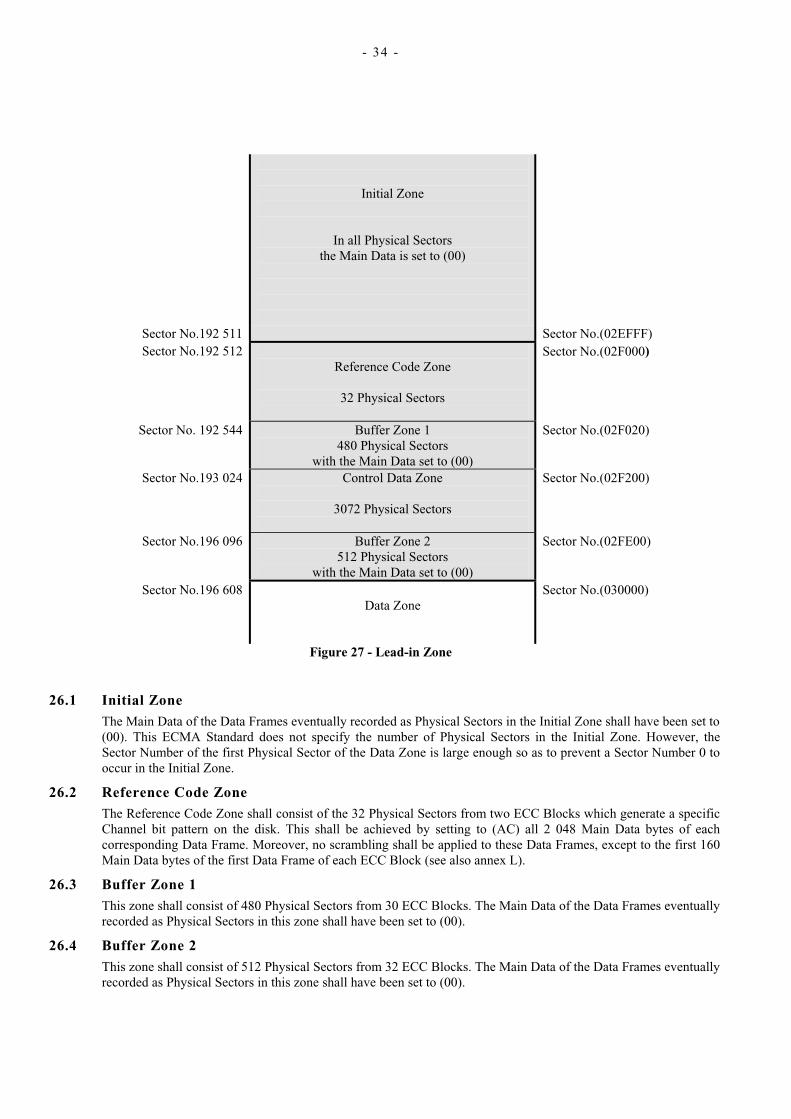
26 Lead-in Zone The Lead-in Zone is the innermost zone of the Information Zone. It shall consist of the following parts (figure 27). The Sector Number of the first Physical Sector of each part is indicated in figure 27 in hexadecimal and in decimal notation.
− Initial Zone, − Reference Code Zone, − Buffer Zone 1, − Control Data Zone, − Buffer Zone 2.
- 34 -
Sector No.192 511
Initial Zone
In all Physical Sectors the Main Data is set to (00)
Sector No.(02EFFF)
Sector No.192 512 Reference Code Zone
32 Physical Sectors
Sector No.(02F000)
Sector No. 192 544 Buffer Zone 1 480 Physical Sectors
with the Main Data set to (00)
Sector No.(02F020)
Sector No.193 024 Control Data Zone
3072 Physical Sectors
Sector No.(02F200)
Sector No.196 096 Buffer Zone 2 512 Physical Sectors
with the Main Data set to (00)
Sector No.(02FE00)
Sector No.196 608 Data Zone
Sector No.(030000)
Figure 27 - Lead-in Zone
26.1 Initial Zone The Main Data of the Data Frames eventually recorded as Physical Sectors in the Initial Zone shall have been set to (00). This ECMA Standard does not specify the number of Physical Sectors in the Initial Zone. However, the Sector Number of the first Physical Sector of the Data Zone is large enough so as to prevent a Sector Number 0 to occur in the Initial Zone.
26.2 Reference Code Zone The Reference Code Zone shall consist of the 32 Physical Sectors from two ECC Blocks which generate a specific Channel bit pattern on the disk. This shall be achieved by setting to (AC) all 2 048 Main Data bytes of each corresponding Data Frame. Moreover, no scrambling shall be applied to these Data Frames, except to the first 160 Main Data bytes of the first Data Frame of each ECC Block (see also annex L).
26.3 Buffer Zone 1 This zone shall consist of 480 Physical Sectors from 30 ECC Blocks. The Main Data of the Data Frames eventually recorded as Physical Sectors in this zone shall have been set to (00).
26.4 Buffer Zone 2 This zone shall consist of 512 Physical Sectors from 32 ECC Blocks. The Main Data of the Data Frames eventually recorded as Physical Sectors in this zone shall have been set to (00).

- 35 -
26.5 Control Data Zone This zone shall consist of 3 072 Physical Sectors from 192 ECC Blocks. The content of the 16 Physical Sectors of each ECC Block is repeated 192 times. The structure of a Control Data Block shall be as shown in figure 28.
Physical format information 2 048 bytes
Disk manufacturing information 2 048 bytes
Content provider information
14 × 2 048 bytes
Figure 28 - Structure of a Control Data Block
26.5.1 Physical format information
This information shall comprise the 2 048 bytes shown in table 6 and described below.
Table 6 - Physical format information
Byte number Content Number of bytes
0 Disk Category and Version Number 1 1 Disk size and maximum transfer rate 1 2 Disk structure 1 3 Recording density 1
4 to 15 Data Zone allocation 12 16 BCA descriptor 1
17 to 31 Reserved 15 32 to 2 047 Reserved 2 016
Byte 0 - Disk Category and Version Number
Bits b0 to b3 shall specify the Version Number
They shall be set to 0001, indicating this ECMA Standard
Bits b4 to b7 shall specify the Disk Category
These bits shall be set to 0000, indicating a read-only disk.
Other settings are prohibited by this ECMA Standard.
Byte 1 - Disk size and maximum transfer rate
Bits b0 to b3 shall specify the maximum transfer rate.
if set to 0000, they specify a maximum transfer rate of 2,52 Mbits/s if set to 0001, they specify a maximum transfer rate of 5,04 Mbits/s if set to 0010, they specify a maximum transfer rate of 10,08 Mbits/s
Bits b4 to b7 shall specify the disk size

- 36 -
They shall be set to 0000, indicating a 120 mm disk
Other settings are prohibited by this ECMA Standard.
Byte 2 - Disk structure
Bits b0 to b3 shall specify the type of the recorded layer(s)
They shall be set to 0001, indicating a read-only layer(s)
Bit b4 shall specify the track path
if set to ZERO, it specifies PTP on DL disks or a SL disk if set to ONE, it specifies OTP on DL disks
Bits b5 and b6 shall specify the disk Type
if set to 00, they specify Type A or Type B if set to 01, they specify Type C or Type D
Bit b7 shall be set to ZERO.
Other settings are prohibited by this ECMA Standard.
Byte 3 - Recording density
Bits b0 to b3 shall specify the average track pitch, they shall be set to 0000, indicating an average track pitch of 0,74 µm
Bits b4 to b7 shall specify the average Channel bit length
if set to 0000, they specify 0,133 µm if set to 0001, they specify 0,147 µm
Other settings are prohibited by this ECMA Standard.
Bytes 4 to 15 - Data Zone allocation
Byte 4 shall be set to (00).
Bytes 5 to 7 shall be set to (030000) to specify the Sector Number 196 608 of the first Physical Sector of the Data Zone
Byte 8 shall be set to (00).
Bytes 9 to 11 shall specify the Sector Number of the last Physical Sector of the Data Zone
Byte 12 shall be set to (00)
Byte 13 to 15 shall be set to (00) on SL disks and DL disks in PTP mode, and to the Sector Number of the last Physical Sector of Layer 0 on DL disks in OTP mode.
Byte 16 - BCA descriptor
This byte shall specify whether or not there is a Burst Cutting Area on the disk.
bits b0 to b6 shall be set to ZERO
bit b7, the BCA flag, shall specify whether or not a BCA exists
if set to ZERO, it shall indicate that a BCA does not exist if set to ONE, it shall indicate that a BCA exists on a Type A or a Type C disk
On Type B and Type D disks, bit7 shall be set to ZERO.
Bytes 17 to 31
These bytes shall be set to (00).

- 37 -
Bytes 32 to 2 047
These bytes shall be set to (00).
26.5.2 Disk manufacturing information
This ECMA Standard does not specify the format and the content of these 2 048 bytes. They shall be ignored in interchange.
26.5.3 Content provider information
The format and the content of these 28 672 bytes require agreement between the interchange parties, else these bytes shall be set to all ZEROs.
27 Middle Zone The Main Data of the Data Frames eventually recorded as Physical Sectors in the Middle Zone shall have been set to (00). This ECMA Standard does not specify the number of Physical Sectors in the Middle Zone.
28 Lead-out Zone The Main Data of the Data Frames eventually recorded as Physical Sectors in the Lead-out Zone shall have been set to (00). This ECMA Standard does not specify the number of Physical Sectors in the Lead-out Zone.

- 38 -
- 39 -
Annex A (normative)
Measurement of the angular deviation αααα
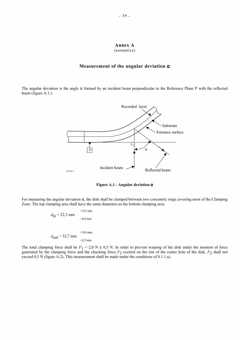
The angular deviation is the angle α formed by an incident beam perpendicular to the Reference Plane P with the reflected beam (figure A.1.).
Figure A.1 - Angular deviation αααα
For measuring the angular deviation α, the disk shall be clamped between two concentric rings covering most of the Clamping Zone. The top clamping area shall have the same diameters as the bottom clamping area.
+ 0,5 mm din = 22,3 mm - 0,0 mm
+ 0,0 mm dout = 32,7 mm - 0,5 mm
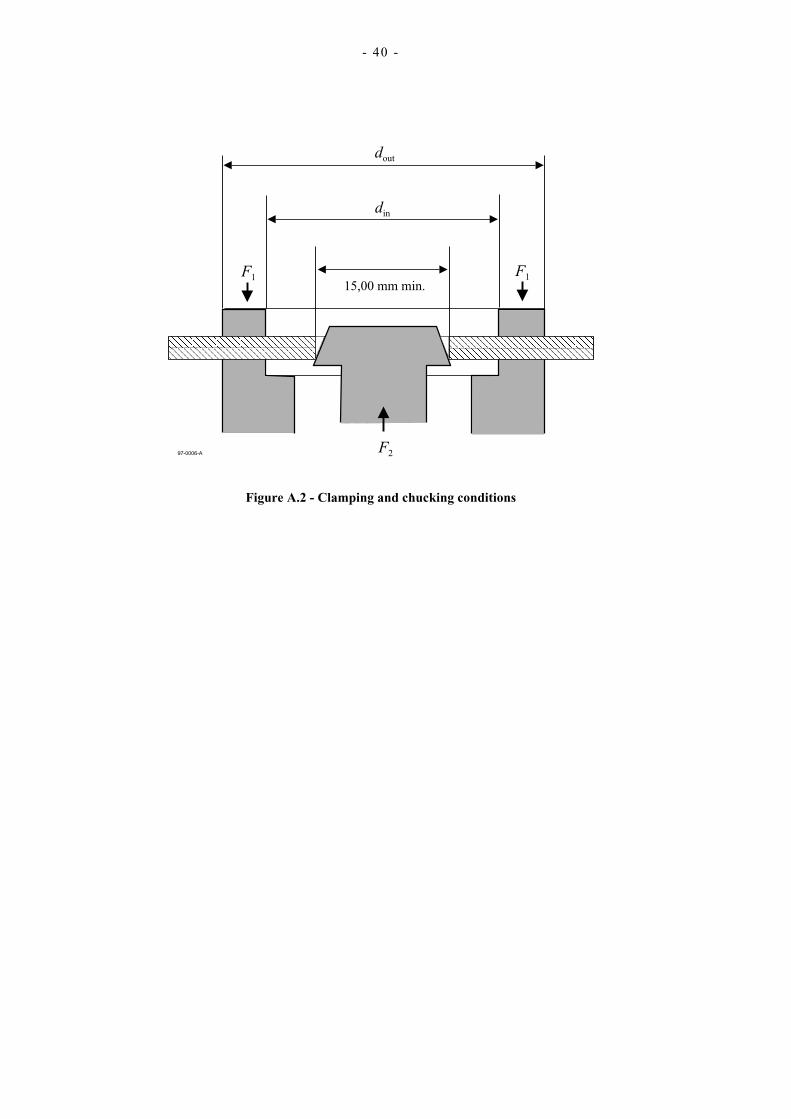
The total clamping force shall be F1 = 2,0 N ± 0,5 N. In order to prevent warping of the disk under the moment of force generated by the clamping force and the chucking force F2 exerted on the rim of the centre hole of the disk, F2 shall not exceed 0,5 N (figure A.2). This measurement shall be made under the conditions of 8.1.1.a).
- 40 -
Figure A.2 - Clamping and chucking conditions

- 41 -
Annex B (normative)
Measurement of birefringence
B.1 Principle of the measurement In order to measure the birefringence, circularly polarized light in a parallel beam is used. The phase retardation is measured by observing the ellipticity of the reflected light.
Figure B.1 - Ellipse with ellipticity e = b/a and orientation θθθθ
The orientation θ of the ellipse is determined by the orientation of the optical axis
θ = γ - π/4 (I)
where γ is the angle between the optical axis and the radial direction.
The ellipticity e = b/a is a function of the phase retardation δ
e = tan 1
2 2
πδ−
(II)
When the phase retardation δ is known the birefringence BR can be expressed as a fraction of the wavelength
BR = λπ
δ2
nm (III)
Thus, by observing the elliptically polarized light reflected from the disk, the birefringence can be measured and the orientation of the optical axis can be assessed as well.
B.2 Measurements conditions The measurement of the birefringence specified above shall be made under the following conditions.
Mode of measurement in reflection, double pass through the substrate
Wavelength λ of the laser light 640 nm ± 15 nm
Beam diameter (FWHM) 1,0 mm ± 0,2 mm
- 42 -
Angle β of incidence in radial direction relative to the radial plane perpendicular to Reference Plane P 7,0° ± 0,2°
Clamping and chucking conditions as specified by annex A
Disk mounting horizontally
Rotation less than 1 Hz
Temperature and relative humidity as specified in 8.1.1)
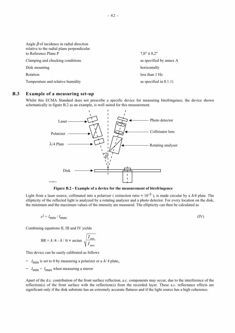
B.3 Example of a measuring set-up Whilst this ECMA Standard does not prescribe a specific device for measuring birefringence, the device shown schematically in figure B.2 as an example, is well suited for this measurement.
Figure B.2 - Example of a device for the measurement of birefringence
Light from a laser source, collimated into a polarizer ( extinction ratio ≈ 10-5 ), is made circular by a λ/4 plate. The ellipticity of the reflected light is analyzed by a rotating analyzer and a photo detector. For every location on the disk, the minimum and the maximum values of the intensity are measured. The ellipticity can then be calculated as
e2 = Imin / Imax (IV)
Combining equations II, III and IV yields
BR = λ /4 - λ / π × arctan I
Imin
max
This device can be easily calibrated as follows
− Imin is set to 0 by measuring a polarizer or a λ/ 4 plate, − Imin = Imax when measuring a mirror
Apart of the d.c. contribution of the front surface reflection, a.c. components may occur, due to the interference of the reflection(s) of the front surface with the reflection(s) from the recorded layer. These a.c. reflectance effects are significant only if the disk substrate has an extremely accurate flatness and if the light source has a high coherence.

- 43 -
Annex C (normative)
Measurement of the differential phase tracking error
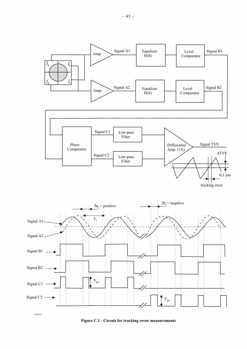
C.1 Measuring method for the differential phase tracking error The reference circuit for the measurement of the tracking error shall be that shown in figure C.1. Each output of the diagonal pairs of elements of the quadrant photo detector shall be digitized independently after equalization of the wave form defined by
H(s) = (1 + 1,6 × 10⁻⁷ iω) / (1 + 4,7 × 10⁻⁸ iω)
The gain of the comparators shall be sufficient to reach full saturation on the outputs, even with minimum signal amplitudes. Phases of the digitized pulse signal edges (signals B1 and B2) shall be compared to each other to produce a time-lead signal C1 and a time-lag signal C2. The phase comparator shall react to each individual edge with signal C1 or C2, depending on the sign of ∆ti. A tracking error signal shall be produced by smoothing the C1, C2 signals with low-pass filters and by substracting by means of a unity gain differential amplifier. The low-pass filters shall be 1st order filters with a cut-off frequency of (-3 dB) 30 kHz.
Special attention shall be given to the implementation of the circuit because very small time differences have to be measured, indeed 1 % of T equals only 0,38 ns. Careful averaging is needed.
The average time difference between two signals from the diagonal pairs of elements of the quadrant detector shall be
∆t = 1/N ∑∆ti
where N is the number of edges both rising and falling.
C.2 Measurement of ∆t /T without time interval analyzer
The relative time difference ∆t /T is represented by the amplitude of the tracking error signal provided that the amplitudes of the C1 and C2 signals and the frequency component of the read-out signals are normalized. The relation
between the tracking error amplitude ∆TVE and the time difference is given by
∆∆ ∆ ∆
TVEt
T
t
N n T T n
i
i
i t= = = ×∑∑
∑Vpc Vpc
Vpc
where
Vpc is the amplitude of the C1 and C2 signals
Ti is the actual length of the read-out signal in the range 3T to 14T
nT is the weighted average value of the actual lengths
N n T is the total averaging time
Assuming that Vpc equals ≈ 5 V and that the measured value of n equals ≈ 5, then the above relation between the
tracking error amplitude ∆TVE and the time difference ∆t can be simplified to
∆TVE = ∆t / T

- 44 -
The specification for the tracking gain can now be rewritten by using the tracking error amplitude as follows
0,5 (Vpc/n) ≤ ∆TVE ≤ 1,1 (Vpc/n)
at 0,1 µm radial offset.
C.3 Calibration of the circuit Assuming that Vpc equals ≈ 5 V and that the measured value of n equals ≈ 5 V, then the above relation between the
tracking error amplitude ∆TVE and the time difference ∆t can be simplified to
∆TVE = ∆t /T × Vpc/n ≈ ∆t /T
The average run length of the 8-to-16 modulated signal is depending on the data content and the averaging time. Therefore, the circuit shall be calibrated with the fixed frequency signal corresponding to a modulated signal with 5T run length. For this purpose sinusoidal signals with a frequency of 2,616 MHz can be used.
Typically the pulse signals C1 and C2 will be generated by a digital gate circuit with an output signal switching between ground and the supply voltage. This voltage swing is assumed to be about 5 V. However, depending on the applied technology it may significantly deviate from 5 V.
Because the formal specification for the DPD signal is
0,5 ≤ ∆t /T ≤ 1,1 at 0,1 µm radial offset,
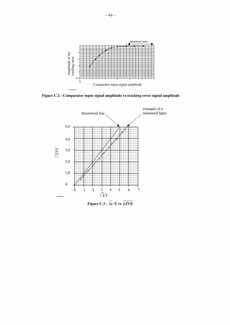
the measurement by means of ∆TVE is influenced by the actual value of Vpc and n. Therefore the following calibration procedure shall apply.
C.3.1 Saturation of the comparators The gain of the level comparators shall be such, that for all actual input signal levels (specially 3T signals) it remains constant. In this case the amplitude of the signal TVE is independent of the amplitude of the input signals, and the gain of the level comparators is in the saturation area (See figure C.2).
C3.2 Correction for n and Vpc Because the above mentioned deviation of n and Vpc, and possibly of some other circuit parameters, a correction factor K has to be determined, such that
∆t /T = K × ∆TVE (measured)
This can be achieved as follows.
a) Generate two sinusoidal signals A1 and A2 of frequency 2,616 MHz with a phase difference, and inject them into the two equalizer circuits.
b) Measure the relation between ∆t /T and ∆TVE and determine K from figure C.3
K = [ ∆t /T(injected)] / [ ∆TVE (measured)]
After the differential amplifier shown in figure C.1, the addition of an amplifier of gain K to the measuring
equipment for the DPD tracking error that adjusts the correction factor K, allows the measurement of ∆t /T directly from the output.
- 45 -
Figure C.1 - Circuit for tracking error measurements
- 46 -
Figure C.2 - Comparator input signal amplitude vs tracking error signal amplitude
5,0
4,0
3,0
2,0
1,0
0
0 1 2 3 4 5 6 7
, t/T
, TV
E
theoretical line
99-0088-A
example of ameasured ligne
Figure C.3 - ∆t /T vs ∆TVE

- 47 -
Annex D (normative)
Measurement of light reflectance
D.1 Calibration method A good reference disk shall be chosen, for instance 0,6 mm glass disk with a golden reflective mirror. This reference disk shall be measured by a parallel beam as shown in figure D.1
Figure D.1 - Reflectance calibration
In this figure the following applies.
I = incident beam
r = reflectance of the entrance surface
Rs = main reflectance of the recorded layer
Rint = other reflectances of the entrance surface and of the recorded layer
R// = measured value, using the arrangement of figure D.1
R// = r + Rs + Rint
r = ( (n-1) / (n+1) )2 where n is the refraction index of the substrate
Rs = R// - r -Rint
Rs = [ (1-r)2 × (R// - r)] / [ 1-r × (2 - R//)]
The reference disk shall be measured on a reference drive and Imirror measured by the focused beam is equated to Rs as determined above.
Now the arrangement is calibrated and the focused reflectivity is a linear function of the reflectivity of the recorded layer, independently from the reflectivity of the entrance surface.

- 48 -
D.2 Measuring method The measuring method comprises the following steps.
a) Measure the reflective light power Ds from the reference disk with calibrated reflectivity Rs
b) Measure I14H in the Information Zone of the disk (see 13.2).
c) Calculate the reflectivity as follows
R RI
DH ss
1414= × H
- 49 -
Annex E (normative)
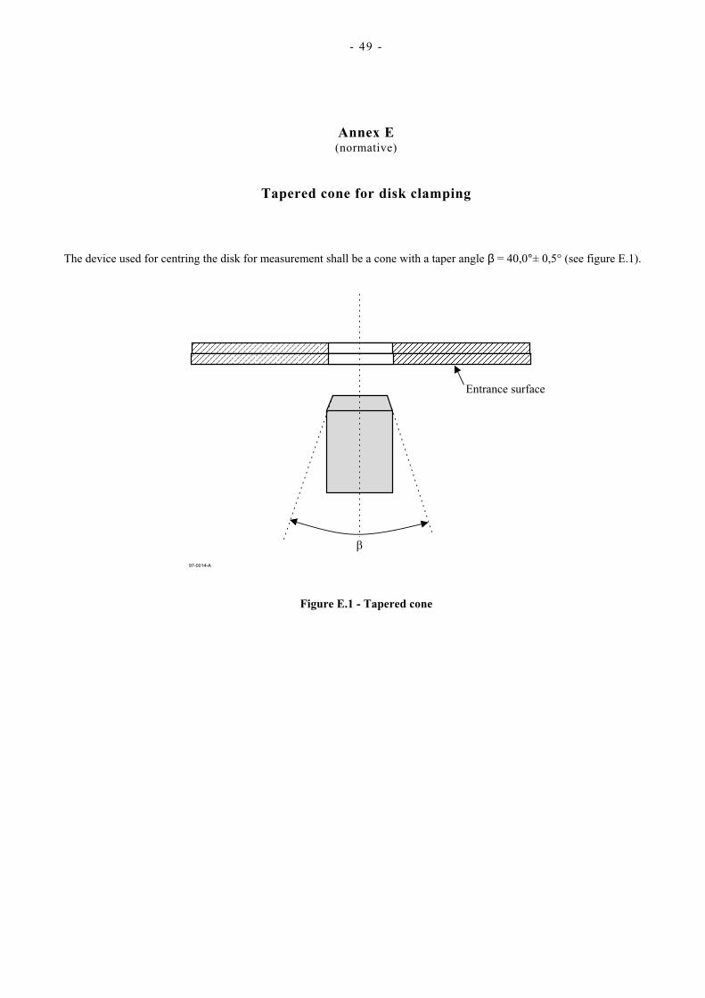
Tapered cone for disk clamping
The device used for centring the disk for measurement shall be a cone with a taper angle β = 40,0°± 0,5° (see figure E.1).
Figure E.1 - Tapered cone

- 50 -

- 51 -
Annex F (normative)
Measurement of jitter
Jitter shall be measured under the conditions of 9.1 with the additional conditions specified in this annex.
F.1 System diagram for jitter measurement The general system diagram for jitter measurement shall be as shown in figure F.1.
Figure F.1 - General diagram for jitter measurement
- 52 -
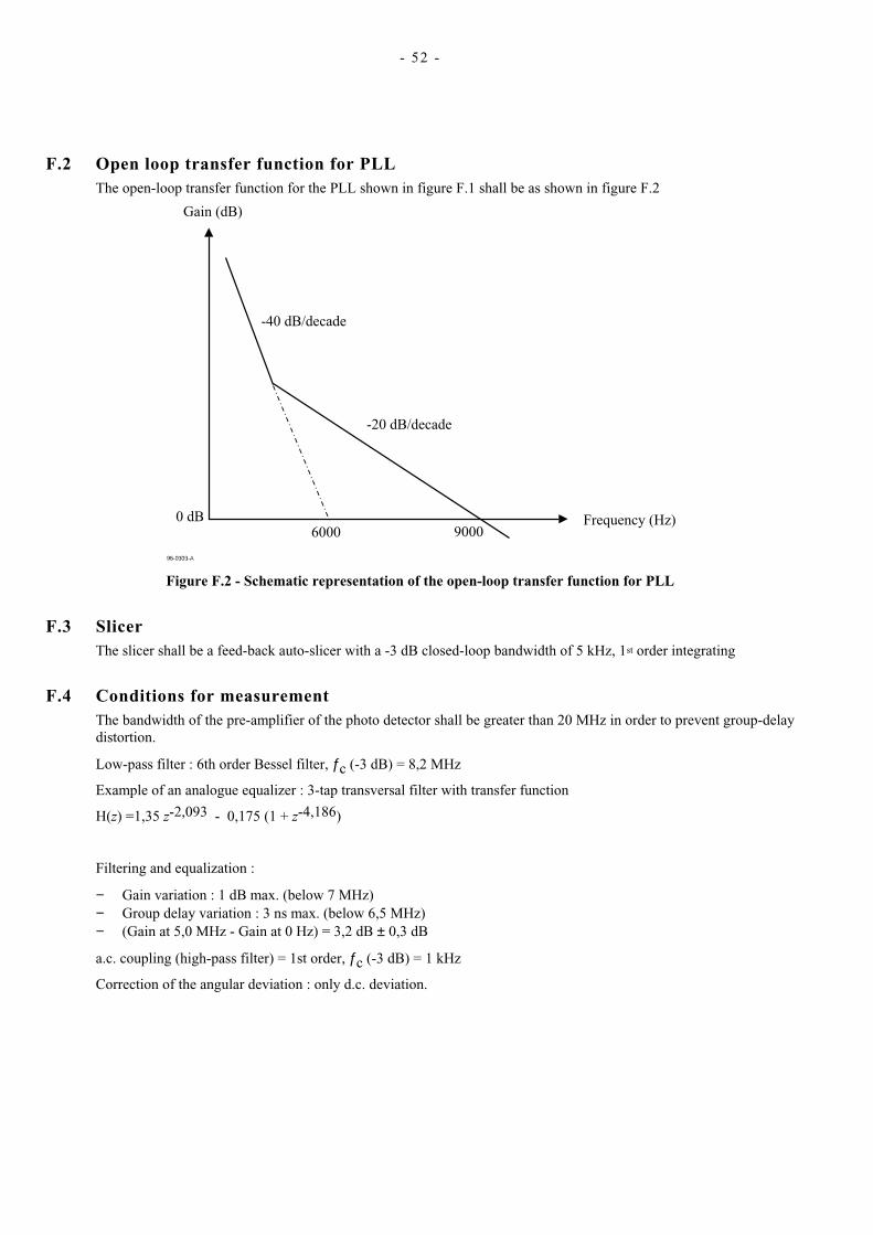
F.2 Open loop transfer function for PLL The open-loop transfer function for the PLL shown in figure F.1 shall be as shown in figure F.2
Figure F.2 - Schematic representation of the open-loop transfer function for PLL
F.3 Slicer The slicer shall be a feed-back auto-slicer with a -3 dB closed-loop bandwidth of 5 kHz, 1st order integrating
F.4 Conditions for measurement The bandwidth of the pre-amplifier of the photo detector shall be greater than 20 MHz in order to prevent group-delay distortion.
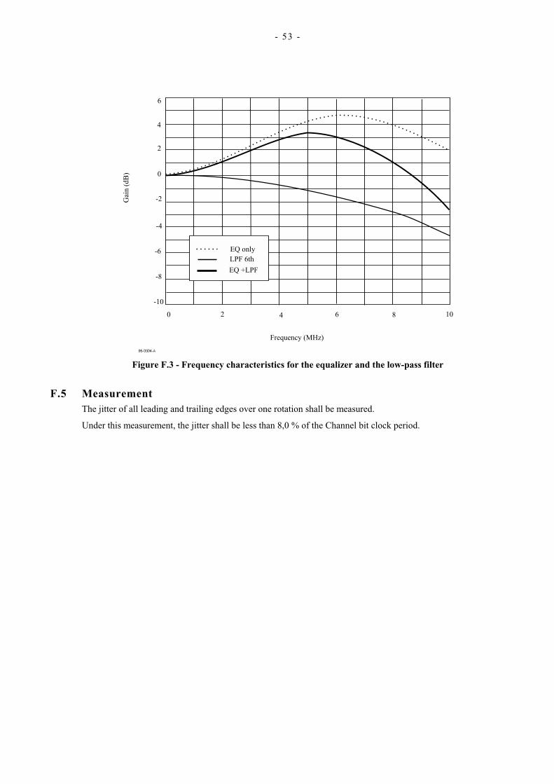
Low-pass filter : 6th order Bessel filter, ƒc (-3 dB) = 8,2 MHz
Example of an analogue equalizer : 3-tap transversal filter with transfer function
H(z) =1,35 z-2,093 - 0,175 (1 + z-4,186)
Filtering and equalization :
− Gain variation : 1 dB max. (below 7 MHz) − Group delay variation : 3 ns max. (below 6,5 MHz) − (Gain at 5,0 MHz - Gain at 0 Hz) = 3,2 dB ± 0,3 dB
a.c. coupling (high-pass filter) = 1st order, ƒc (-3 dB) = 1 kHz
Correction of the angular deviation : only d.c. deviation.
- 53 -
Figure F.3 - Frequency characteristics for the equalizer and the low-pass filter
F.5 Measurement The jitter of all leading and trailing edges over one rotation shall be measured.
Under this measurement, the jitter shall be less than 8,0 % of the Channel bit clock period.

- 54 -
- 55 -
Annex G (normative)
8-to-16 Modulation with RLL (2,10) requirements
Tables G.1 and G.2 list the 16-bit Code Words into which the 8-bit coded Data bytes have to be transformed. Figure G.1 shows schematically how the Code Words and the associated State specification are generated.
Figure G.1 - Code Words generation
In this figure :
X(t) = H {B(t), S(t)} X15(t) = msb and X0(t) = lsb S(t+1) =G{B(t), S(t)} H is the output function G is the next-state function
The Code Words leaving the States shall be chosen so that the concatenation of Code Words entering a State and those leaving that State satisfy the requirement that between two ONEs there shall be at least 2 and at most 10 ZEROs.
As additional requirements:
− Code Words leaving State 2 shall have both bit x15 and bit x3 set to ZERO, and − in Code Words leaving State 3 bit x15 or bit x3 or both shall be set to ONE.
This means that the Code Word sets of States 2 and 3 are disjoint.

- 56 -
Code Word X(t)
Next State S(t+1) Code Word X(t+1)
Ends with 1 or no trailing ZERO
State 1 Starts with 2 or up to 9 leading ZEROs
Ends with 2 or up to 5 trailing ZEROs State 2 Starts with 1 or up to 5 leading ZEROs, and X15(t+1),X3(t+1) = 0,0
Ends with 2 or up to 5 trailing ZEROs State 3 Starts with none or up to 5 leading ZEROs, and X15(t+1),X3(t+1) ≠ 0,0
Ends with 6 or up to 9 trailing ZEROs
State 4 Starts with 1 or no leading ZERO
Figure G.2 - Determination of States
Note that when decoding the recorded data, knowledge about the encoder is required to be able to reconstitute the original main Data.
B(t) = H-1 {X(t), S(t)}
Because of the involved error propagation, such state-dependent decoding is to be avoided. In the case of this 8-to-16 modulation, the conversion tables have been chosen in such a way that knowledge about the State is not required in most cases. As can be gathered from the tables, in some cases, two 8-bit bytes, for instance the 8-bit bytes 5 and 6 in States 1 and 2 in table G.1, generate the same 16-bit Code Words. The construction of the tables allows to solve this apparent ambiguity. Indeed, if two identical Code Words leave a State, one of them goes to State 2 and the other to State 3. Because the setting of bits X15 and X3 is always different in these two States, any Code Word can be uniquely decoded by analysing the Code Word itself together with bits X15 and X3 of the next Code Word :
B(t) = H-1 { X(t), X15(t+1), X3(t+1) }
In the tables, the 8-bit bytes are identified by their decimal value.
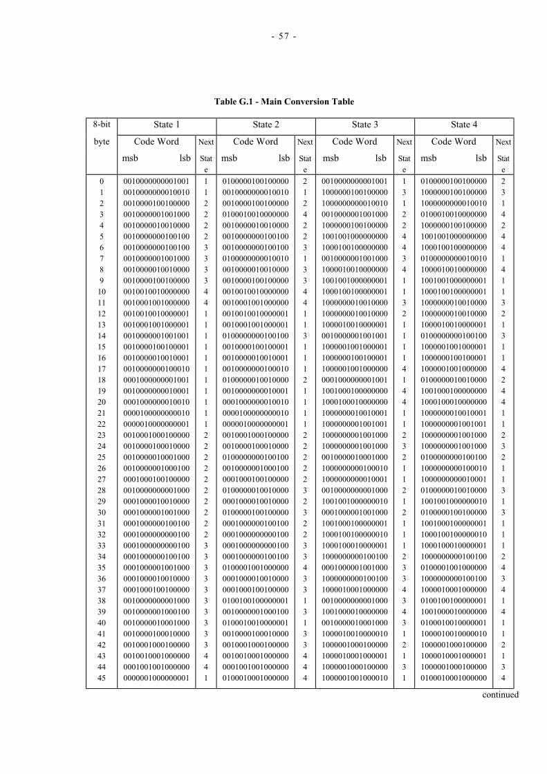
- 57 -
Table G.1 - Main Conversion Table
8-bit State 1 State 2 State 3 State 4
byte Code Word Next Code Word Next Code Word Next Code Word Next
msb lsb State
msb lsb State
msb lsb State
msb lsb State
0 1 2 3 4 5 6 7 8 9
10 11 12 13 14 15 16 17 18 19 20 21 22 23 24 25 26 27 28 29 30 31 32 33 34 35 36 37 38 39 40 41 42 43 44 45
0010000000001001 0010000000010010 0010000100100000 0010000001001000 0010000010010000 0010000000100100 0010000000100100 0010000001001000 0010000010010000 0010000100100000 0010010010000000 0010001001000000 0010010010000001 0010001001000001 0010000001001001 0010000100100001 0010000010010001 0010000000100010 0001000000001001 0010000000010001 0001000000010010 0000100000000010 0000010000000001 0010001000100000 0010000100010000 0010000010001000 0010000001000100 0001000100100000 0010000000001000 0001000010010000 0001000001001000 0001000000100100 0001000000000100 0001000000000100 0001000000100100 0001000001001000 0001000010010000 0001000100100000 0010000000001000 0010000001000100 0010000010001000 0010000100010000 0010001000100000 0010010001000000 0001001001000000 0000001000000001
1 1 2 2 2 2 3 3 3 3 4 4 1 1 1 1 1 1 1 1 1 1 1 2 2 2 2 2 2 2 2 2 2 3 3 3 3 3 3 3 3 3 3 4 4 1
0100000100100000 0010000000010010 0010000100100000 0100010010000000 0010000010010000 0010000000100100 0010000000100100 0100000000010010 0010000010010000 0010000100100000 0010010010000000 0010001001000000 0010010010000001 0010001001000001 0100000000100100 0010000100100001 0010000010010001 0010000000100010 0100000010010000 0010000000010001 0001000000010010 0000100000000010 0000010000000001 0010001000100000 0010000100010000 0100000000100100 0010000001000100 0001000100100000 0100000010010000 0001000010010000 0100000100100000 0001000000100100 0001000000000100 0001000000000100 0001000000100100 0100001001000000 0001000010010000 0001000100100000 0100100100000001 0010000001000100 0100010010000001 0010000100010000 0010001000100000 0010010001000000 0001001001000000 0100010001000000
2 1 2 4 2 2 3 1 3 3 4 4 1 1 3 1 1 1 2 1 1 1 1 2 2 2 2 2 3 2 3 2 2 3 3 4 3 3 1 3 1 3 3 4 4 4
0010000000001001 1000000100100000 1000000000010010 0010000001001000 1000000100100000 1001001000000000 1000100100000000 0010000001001000 1000010010000000 1001001000000001 1000100100000001 1000000010010000 1000000010010000 1000010010000001 0010000001001001 1000001001000001 1000000100100001 1000001001000000 0001000000001001 1001000100000000 1000100010000000 1000000010010001 1000000001001001 1000000001001000 1000000001001000 0010000010001000 1000000000100010 1000000000010001 0010000000001000 1001001000000010 0001000001001000 1001000100000001 1000100100000010 1000100010000001 1000000000100100 0001000001001000 1000000000100100 1000010001000000 0010000000001000 1001000010000000 0010000010001000 1000010010000010 1000001000100000 1000010001000001 1000001000100000 1000001001000010
1 3 1 2 2 4 4 3 4 1 1 3 2 1 1 1 1 4 1 4 4 1 1 2 3 2 1 1 2 1 2 1 1 1 2 3 3 4 3 4 3 1 2 1 3 1
0100000100100000 1000000100100000 1000000000010010 0100010010000000 1000000100100000 1001001000000000 1000100100000000 0100000000010010 1000010010000000 1001001000000001 1000100100000001 1000000010010000 1000000010010000 1000010010000001 0100000000100100 1000001001000001 1000000100100001 1000001001000000 0100000010010000 1001000100000000 1000100010000000 1000000010010001 1000000001001001 1000000001001000 1000000001001000 0100000000100100 1000000000100010 1000000000010001 0100000010010000 1001001000000010 0100000100100000 1001000100000001 1000100100000010 1000100010000001 1000000000100100 0100001001000000 1000000000100100 1000010001000000 0100100100000001 1001000010000000 0100010010000001 1000010010000010 1000001000100000 1000010001000001 1000001000100000 0100010001000000
2 3 1 4 2 4 4 1 4 1 1 3 2 1 3 1 1 4 2 4 4 1 1 2 3 2 1 1 3 1 3 1 1 1 2 4 3 4 1 4 1 1 2 1 3 4
continued
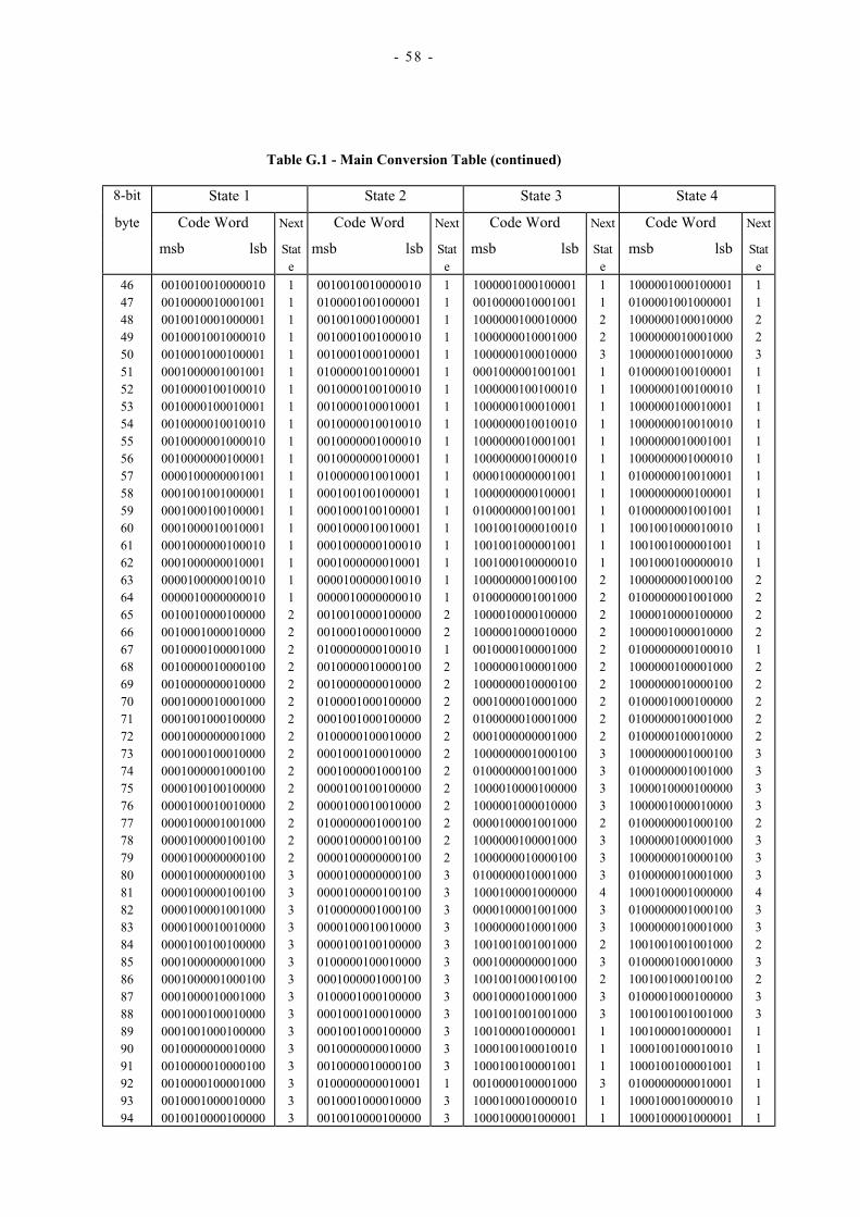
- 58 -
Table G.1 - Main Conversion Table (continued)
8-bit State 1 State 2 State 3 State 4
byte Code Word Next Code Word Next Code Word Next Code Word Next
msb lsb State
msb lsb State
msb lsb State
msb lsb State
46 47 48 49 50 51 52 53 54 55 56 57 58 59 60 61 62 63 64 65 66 67 68 69 70 71 72 73 74 75 76 77 78 79 80 81 82 83 84 85 86 87 88 89 90 91 92 93 94
0010010010000010 0010000010001001 0010010001000001 0010001001000010 0010001000100001 0001000001001001 0010000100100010 0010000100010001 0010000010010010 0010000001000010 0010000000100001 0000100000001001 0001001001000001 0001000100100001 0001000010010001 0001000000100010 0001000000010001 0000100000010010 0000010000000010 0010010000100000 0010001000010000 0010000100001000 0010000010000100 0010000000010000 0001000010001000 0001001000100000 0001000000001000 0001000100010000 0001000001000100 0000100100100000 0000100010010000 0000100001001000 0000100000100100 0000100000000100 0000100000000100 0000100000100100 0000100001001000 0000100010010000 0000100100100000 0001000000001000 0001000001000100 0001000010001000 0001000100010000 0001001000100000 0010000000010000 0010000010000100 0010000100001000 0010001000010000 0010010000100000
1 1 1 1 1 1 1 1 1 1 1 1 1 1 1 1 1 1 1 2 2 2 2 2 2 2 2 2 2 2 2 2 2 2 3 3 3 3 3 3 3 3 3 3 3 3 3 3 3
0010010010000010 0100001001000001 0010010001000001 0010001001000010 0010001000100001 0100000100100001 0010000100100010 0010000100010001 0010000010010010 0010000001000010 0010000000100001 0100000010010001 0001001001000001 0001000100100001 0001000010010001 0001000000100010 0001000000010001 0000100000010010 0000010000000010 0010010000100000 0010001000010000 0100000000100010 0010000010000100 0010000000010000 0100001000100000 0001001000100000 0100000100010000 0001000100010000 0001000001000100 0000100100100000 0000100010010000 0100000001000100 0000100000100100 0000100000000100 0000100000000100 0000100000100100 0100000001000100 0000100010010000 0000100100100000 0100000100010000 0001000001000100 0100001000100000 0001000100010000 0001001000100000 0010000000010000 0010000010000100 0100000000010001 0010001000010000 0010010000100000
1 1 1 1 1 1 1 1 1 1 1 1 1 1 1 1 1 1 1 2 2 1 2 2 2 2 2 2 2 2 2 2 2 2 3 3 3 3 3 3 3 3 3 3 3 3 1 3 3
1000001000100001 0010000010001001 1000000100010000 1000000010001000 1000000100010000 0001000001001001 1000000100100010 1000000100010001 1000000010010010 1000000010001001 1000000001000010 0000100000001001 1000000000100001 0100000001001001 1001001000010010 1001001000001001 1001000100000010 1000000001000100 0100000001001000 1000010000100000 1000001000010000 0010000100001000 1000000100001000 1000000010000100 0001000010001000 0100000010001000 0001000000001000 1000000001000100 0100000001001000 1000010000100000 1000001000010000 0000100001001000 1000000100001000 1000000010000100 0100000010001000 1000100001000000 0000100001001000 1000000010001000 1001001001001000 0001000000001000 1001001000100100 0001000010001000 1001001001001000 1001000010000001 1000100100010010 1000100100001001 0010000100001000 1000100010000010 1000100001000001
1 1 2 2 3 1 1 1 1 1 1 1 1 1 1 1 1 2 2 2 2 2 2 2 2 2 2 3 3 3 3 2 3 3 3 4 3 3 2 3 2 3 3 1 1 1 3 1 1
1000001000100001 0100001001000001 1000000100010000 1000000010001000 1000000100010000 0100000100100001 1000000100100010 1000000100010001 1000000010010010 1000000010001001 1000000001000010 0100000010010001 1000000000100001 0100000001001001 1001001000010010 1001001000001001 1001000100000010 1000000001000100 0100000001001000 1000010000100000 1000001000010000 0100000000100010 1000000100001000 1000000010000100 0100001000100000 0100000010001000 0100000100010000 1000000001000100 0100000001001000 1000010000100000 1000001000010000 0100000001000100 1000000100001000 1000000010000100 0100000010001000 1000100001000000 0100000001000100 1000000010001000 1001001001001000 0100000100010000 1001001000100100 0100001000100000 1001001001001000 1001000010000001 1000100100010010 1000100100001001 0100000000010001 1000100010000010 1000100001000001
1 1 2 2 3 1 1 1 1 1 1 1 1 1 1 1 1 2 2 2 2 1 2 2 2 2 2 3 3 3 3 2 3 3 3 4 3 3 2 3 2 3 3 1 1 1 1 1 1
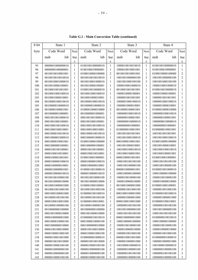
- 59 -
Table G.1 - Main Conversion Table (continued)
8-bit State 1 State 2 State 3 State 4
byte Code Word Next Code Word Next Code Word Next Code Word Next
msb lsb State
msb lsb State
msb lsb State
msb lsb State
95 96 97 98 99 100 101 102 103 104 105 106 107 108 109 110 111 112 113 114 115 116 117 118 119 120 121 122 123 124 125 126 127 128 129 130 131 132 133 134 135 136 137 138 139 140 141 142 143
0000001000000010 0000000100000001 0010010010001001 0010010010010010 0010010001000010 0010010000100001 0010001001001001 0010001000100010 0010001000010001 0010000100010010 0010000010000010 0010000100001001 0010000001000001 0001001001000010 0001001000100001 0001000100100010 0001000100010001 0001000010010010 0001000001000010 0001000010001001 0001000000100001 0000100100100001 0000100010010001 0000100001001001 0000100000100010 0000100000010001 0000010000001001 0000010000010010 0010010010000100 0010010000010000 0010001000001000 0010001001000100 0001000100001000 0010000100100100 0000100010001000 0010000100000100 0010000000100000 0001001000010000 0000100000001000 0001000010000100 0001000000010000 0000100100010000 0000100001000100 0000010001001000 0000010010010000 0000010000100100 0000010000000100 0000010000000100 0000010000100100
1 1 1 1 1 1 1 1 1 1 1 1 1 1 1 1 1 1 1 1 1 1 1 1 1 1 1 1 2 2 2 2 2 2 2 2 2 2 2 2 2 2 2 2 2 2 2 3 3
0100100100000010 0100100010000001 0100010000100000 0010010010010010 0010010001000010 0010010000100001 0100010010000010 0010001000100010 0010001000010001 0010000100010010 0010000010000010 0100001000010000 0010000001000001 0001001001000010 0001001000100001 0001000100100010 0001000100010001 0001000010010010 0001000001000010 0100010000100000 0001000000100001 0000100100100001 0000100010010001 0100010001000001 0000100000100010 0000100000010001 0100001001000010 0000010000010010 0010010010000100 0010010000010000 0100001000100001 0010001001000100 0100000100100010 0010000100100100 0100000100010001 0010000100000100 0010000000100000 0001001000010000 0100000010010010 0001000010000100 0001000000010000 0000100100010000 0000100001000100 0100000001000010 0000010010010000 0000010000100100 0000010000000100 0000010000000100 0000010000100100
1 1 2 1 1 1 1 1 1 1 1 2 1 1 1 1 1 1 1 3 1 1 1 1 1 1 1 1 2 2 1 2 1 2 1 2 2 2 1 2 2 2 2 1 2 2 2 3 3
1000010010010010 1000010010001001 0010010010001001 1001001000000100 1001001000100100 1000010001000010 0010001001001001 1000010000100001 1000001001001001 1000001000100010 1000001000010001 0010000100001001 1000000100010010 1000000100001001 1000000010000010 1000000001000001 0100000010001001 1001001001001001 1001001000100010 0001000010001001 1001001000010001 1001000100010010 1001000100001001 0000100001001001 1000100100100100 1000100100000100 0000010000001001 1000100000100000 1000010010000100 1000010000010000 0010001000001000 1000001001000100 0001000100001000 1000001000001000 0000100010001000 1000000100100100 1001001000000100 1000100100100100 0000100000001000 1000100000100000 1000010010000100 1000010000010000 1000001001000100 0000010001001000 1000001000001000 1001000010000010 1000000100000100 1000000100100100 1000000100000100
1 1 1 2 3 1 1 1 1 1 1 1 1 1 1 1 1 1 1 1 1 1 1 1 2 2 1 2 2 2 2 2 2 2 2 2 3 3 2 3 3 3 3 2 3 1 2 3 3
0100100100000010 0100100010000001 0100010000100000 1001001000000100 1001001000100100 1000010001000010 0100010010000010 1000010000100001 1000001001001001 1000001000100010 1000001000010001 0100001000010000 1000000100010010 1000000100001001 1000000010000010 1000000001000001 0100000010001001 1001001001001001 1001001000100010 0100010000100000 1001001000010001 1001000100010010 1001000100001001 0100010001000001 1000100100100100 1000100100000100 0100001001000010 1000100000100000 1000010010000100 1000010000010000 0100001000100001 1000001001000100 0100000100100010 1000001000001000 0100000100010001 1000000100100100 1001001000000100 1000100100100100 0100000010010010 1000100000100000 1000010010000100 1000010000010000 1000001001000100 0100000001000010 1000001000001000 1001000010000010 1000000100000100 1000000100100100 1000000100000100
1 1 2 2 3 1 1 1 1 1 1 2 1 1 1 1 1 1 1 3 1 1 1 1 2 2 1 2 2 2 1 2 1 2 1 2 3 3 1 3 3 3 3 1 3 1 2 3 3
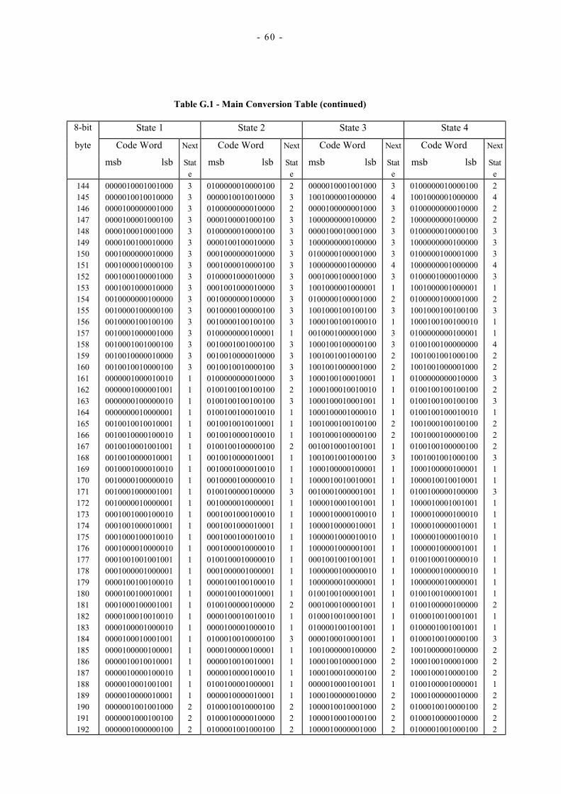
- 60 -
Table G.1 - Main Conversion Table (continued)
8-bit State 1 State 2 State 3 State 4
byte Code Word Next Code Word Next Code Word Next Code Word Next
msb lsb State
msb lsb State
msb lsb State
msb lsb State
144 145 146 147 148 149 150 151 152 153 154 155 156 157 158 159 160 161 162 163 164 165 166 167 168 169 170 171 172 173 174 175 176 177 178 179 180 181 182 183 184 185 186 187 188 189 190 191 192
0000010001001000 0000010010010000 0000100000001000 0000100001000100 0000100010001000 0000100100010000 0001000000010000 0001000010000100 0001000100001000 0001001000010000 0010000000100000 0010000100000100 0010000100100100 0010001000001000 0010001001000100 0010010000010000 0010010010000100 0000001000010010 0000001000001001 0000000100000010 0000000010000001 0010010010010001 0010010000100010 0010010001001001 0010010000010001 0010001000010010 0010000100000010 0010001000001001 0010000010000001 0001001000100010 0001001000010001 0001000100010010 0001000010000010 0001001001001001 0001000001000001 0000100100100010 0000100100010001 0001000100001001 0000100010010010 0000100001000010 0000100010001001 0000100000100001 0000010010010001 0000010000100010 0000010001001001 0000010000010001 0000001001001000 0000001000100100 0000001000000100
3 3 3 3 3 3 3 3 3 3 3 3 3 3 3 3 3 1 1 1 1 1 1 1 1 1 1 1 1 1 1 1 1 1 1 1 1 1 1 1 1 1 1 1 1 1 2 2 2
0100000010000100 0000010010010000 0100000000010000 0000100001000100 0100000010000100 0000100100010000 0001000000010000 0001000010000100 0100001000010000 0001001000010000 0010000000100000 0010000100000100 0010000100100100 0100000000100001 0010001001000100 0010010000010000 0010010010000100 0100000000010000 0100100100100100 0100100100100100 0100100100010010 0010010010010001 0010010000100010 0100100100000100 0010010000010001 0010001000010010 0010000100000010 0100100000100000 0010000010000001 0001001000100010 0001001000010001 0001000100010010 0001000010000010 0100100010000010 0001000001000001 0000100100100010 0000100100010001 0100100000100000 0000100010010010 0000100001000010 0100010010000100 0000100000100001 0000010010010001 0000010000100010 0100100001000001 0000010000010001 0100010010000100 0100010000010000 0100001001000100
2 3 2 3 3 3 3 3 3 3 3 3 3 1 3 3 3 3 2 3 1 1 1 2 1 1 1 3 1 1 1 1 1 1 1 1 1 2 1 1 3 1 1 1 1 1 2 2 2
0000010001001000 1001000001000000 0000100000001000 1000000000100000 0000100010001000 1000000000100000 0100000100001000 1000000001000000 0001000100001000 1001000001000001 0100000100001000 1001000100100100 1000100100100010 0010001000001000 1000100100000100 1001001001000100 1001001000001000 1000100100010001 1000100010010010 1000100010001001 1000100001000010 1001000100100100 1001000100000100 0010010001001001 1001001001000100 1000100000100001 1000010010010001 0010001000001001 1000010001001001 1000010000100010 1000010000010001 1000001000010010 1000001000001001 0001001001001001 1000000100000010 1000000010000001 0100100100001001 0001000100001001 0100010010001001 0100001001001001 0000100010001001 1001000000100000 1000100100001000 1000100010000100 0000010001001001 1000100000010000 1000010010001000 1000010001000100 1000010000001000
3 4 3 2 3 3 3 4 3 1 2 3 1 3 3 2 2 1 1 1 1 2 2 1 3 1 1 1 1 1 1 1 1 1 1 1 1 1 1 1 1 2 2 2 1 2 2 2 2
0100000010000100 1001000001000000 0100000000010000 1000000000100000 0100000010000100 1000000000100000 0100000100001000 1000000001000000 0100001000010000 1001000001000001 0100000100001000 1001000100100100 1000100100100010 0100000000100001 0100100100000000 1001001001000100 1001001000001000 0100000000010000 0100100100100100 0100100100100100 0100100100010010 1001000100100100 1001000100000100 0100100100000100 1001001001000100 1000100000100001 1000010010010001 0100100000100000 1000010001001001 1000010000100010 1000010000010001 1000001000010010 1000001000001001 0100100010000010 1000000100000010 1000000010000001 0100100100001001 0100100000100000 0100010010001001 0100001001001001 0100010010000100 1001000000100000 1000100100001000 1000100010000100 0100100001000001 1000100000010000 0100010010000100 0100010000010000 0100001001000100
2 4 2 2 3 3 3 4 3 1 2 3 1 1 4 2 2 3 2 3 1 2 2 2 3 1 1 3 1 1 1 1 1 1 1 1 1 2 1 1 3 2 2 2 1 2 2 2 2
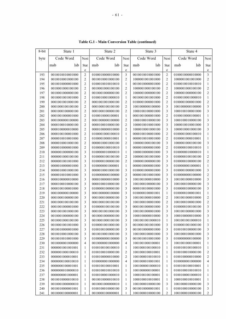
- 61 -
Table G.1 - Main Conversion Table (continued)
8-bit State 1 State 2 State 3 State 4
byte Code Word Next Code Word Next Code Word Next Code Word Next
msb lsb State
msb lsb State
msb lsb State
msb lsb State
193 194 195 196 197 198 199 200 201 202 203 204 205 206 207 208 209 210 211 212 213 214 215 216 217 218 219 220 221 222 223 224 225 226 227 228 229 230 231 232 233 234 235 236 237 238 239 240 241
0010010010001000 0010010001000100 0010010000001000 0010001000100100 0010001000000100 0010001001001000 0001001001000100 0001000100100100 0001000100000100 0001001000001000 0001000000100000 0000100010000100 0000100000010000 0000100100001000 0000010010001000 0000010001000100 0000010000001000 0000001000000100 0000001000100100 0000001001001000 0000010000001000 0000010001000100 0000010010001000 0000100000010000 0000100010000100 0000100100001000 0001000000100000 0001000100000100 0001000100100100 0001001000001000 0001001001000100 0010001000000100 0010001000100100 0010001001001000 0010010000001000 0010010001000100 0010010010001000 0010000001000000 0000001001001001 0000001000100010 0000001000010001 0000000100010010 0000000100001001 0000000010000010 0000000001000001 0010010000010010 0010001000000010 0010010000001001 0010000100000001
2 2 2 2 2 2 2 2 2 2 2 2 2 2 2 2 2 3 3 3 3 3 3 3 3 3 3 3 3 3 3 3 3 3 3 3 3 4 1 1 1 1 1 1 1 1 1 1 1
0100010000010000 0010010001000100 0100010010010010 0010001000100100 0010001000000100 0100010001000010 0001001001000100 0001000100100100 0001000100000100 0100010000100001 0001000000100000 0000100010000100 0000100000010000 0100001000100010 0100001000010001 0000010001000100 0100000100010010 0100000010000010 0100000100100100 0100000100000100 0100000001000001 0000010001000100 0100000000100000 0000100000010000 0000100010000100 0100000100000100 0001000000100000 0001000100000100 0001000100100100 0100000100100100 0001001001000100 0010001000000100 0010001000100100 0100001001000100 0100100100000100 0010010001000100 0100000000100000 0010000001000000 0100100100100010 0100100010000100 0100100000010000 0100000001000000 0100100100010001 0100100010010010 0100100001000010 0010010000010010 0010001000000010 0100100010000100 0010000100000001
3 2 1 2 2 1 2 2 2 1 2 2 2 1 1 2 1 1 2 2 1 3 2 3 3 3 3 3 3 3 3 3 3 3 3 3 3 4 1 2 2 4 1 1 1 1 1 3 1
0010010010001000 1000001001001000 0010010000001000 1000001000100100 1000001000000100 0010001001001000 0100001000001000 1001000000100000 1000100100001000 0001001000001000 1000100010000100 1000010010001000 1000010001000100 0000100100001000 0000010010001000 1000001000100100 0000010000001000 1000010000001000 1000001001001000 1000001000000100 0000010000001000 0100001000001000 0000010010001000 1001001000010000 1001000100000100 0000100100001000 0100000100001001 1001001000010000 1001000100001000 0001001000001000 1001001000001000 1000100000010000 1001001001000010 0010001001001000 0010010000001000 1001000100001000 0010010010001000 1001001000100001 1001000100100010 1001000100010001 1001000010010010 1001000010001001 1001000001000010 1001000000100001 1000100100100001 1000100010010001 1001000010000100 0010010000001001 1001000010000100
2 2 2 2 2 2 2 3 3 2 3 3 3 2 2 3 2 3 3 3 3 3 3 3 3 3 1 2 2 3 3 3 1 3 3 3 3 1 1 1 1 1 1 1 1 1 3 1 2
0100010000010000 1000001001001000 0100010010010010 1000001000100100 1000001000000100 0100010001000010 0100001000001000 1001000000100000 1000100100001000 0100010000100001 1000100010000100 1000010010001000 1000010001000100 0100001000100010 0100001000010001 1000001000100100 0100000100010010 0100000010000010 0100000100100100 0100000100000100 0100000001000001 0100001000001000 0100000000100000 1001001000010000 1001000100000100 0100000100000100 0100000100001001 1001001000010000 1001000100001000 0100000100100100 1001001000001000 1000100000010000 1001001001000010 0100001001000100 0100100100000100 1001000100001000 0100000000100000 1001001000100001 0100100100100010 0100100010000100 0100100000010000 0100000001000000 0100100100010001 0100100010010010 0100100001000010 1000100010010001 1001000010000100 0100100010000100 1001000010000100
3 2 1 2 2 1 2 3 3 1 3 3 3 1 1 3 1 1 2 2 1 3 2 3 3 3 1 2 2 3 3 3 1 3 3 3 3 1 1 2 2 4 1 1 1 1 3 3 2
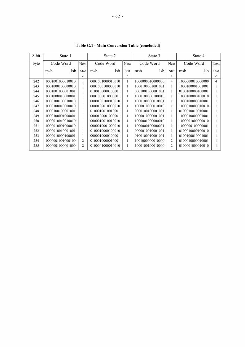
- 62 -
Table G.1 - Main Conversion Table (concluded)
8-bit State 1 State 2 State 3 State 4
byte Code Word Next Code Word Next Code Word Next Code Word Next
msb lsb State
msb lsb State
msb lsb State
msb lsb State
242 243 244 245 246 247 248 249 250 251 252 253 254 255
0001001000010010 0001000100000010 0001001000001001 0001000010000001 0000100100010010 0000100010000010 0000100100001001 0000100001000001 0000010010010010 0000010001000010 0000010010001001 0000010000100001 0000001001000100 0000001000001000
1 1 1 1 1 1 1 1 1 1 1 1 2 2
0001001000010010 0001000100000010 0100100000100001 0001000010000001 0000100100010010 0000100010000010 0100010010010001 0000100001000001 0000010010010010 0000010001000010 0100010000100010 0000010000100001 0100010000010001 0100001000010010
1 1 1 1 1 1 1 1 1 1 1 1 1 1
1000000010000000 1000100001001001 0001001000001001 1000100000100010 1000100000010001 1000010000010010 0000100100001001 1000010000001001 1000001000000010 1000000100000001 0000010010001001 0100100010001001 1001000000010000 1000100100010000
4 1 1 1 1 1 1 1 1 1 1 1 2 2
1000000010000000 1000100001001001 0100100000100001 1000100000100010 1000100000010001 1000010000010010 0100010010010001 1000010000001001 1000001000000010 1000000100000001 0100010000100010 0100100010001001 0100010000010001 0100001000010010
4 1 1 1 1 1 1 1 1 1 1 1 1 1
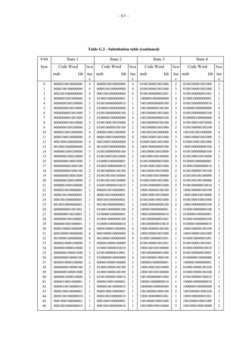
- 63 -
Table G.2 - Substitution table (continued)
8-bit State 1 State 2 State 3 State 4
byte Code Word Next Code Word Next Code Word Next Code Word Next
msb lsb State
msb lsb State
msb lsb State
msb lsb State
0 1 2 3 4 5 6 7 8 9
10 11 12 13 14 15 16 17 18 19 20 21 22 23 24 25 26 27 28 29 30 31 32 33 34 35 36 37 38 39 40 41 42 43 44 45 46
0000010010000000 0000100100000000 0001001000000000 0000001001000000 0000000100100000 0000000010010000 0000000001001000 0000000001001000 0000000010010000 0000000100100000 0000010001000000 0000100010000000 0001000100000000 0010001000000000 0000001000100000 0000000100010000 0000000010001000 0000000001000100 0000000001000100 0000000010001000 0000000100010000 0000001000100000 0000010010000001 0000100100000001 0001001000000001 0010010000000001 0000000001001001 0000000010010001 0000000100100001 0000001001000001 0000100001000000 0001000010000000 0010000100000000 0000010000100000 0000001000010000 0000000100001000 0000000010000100 0000010000100000 0000000010000100 0000000100001000 0000001000010000 0000010001000001 0000010010000010 0000100010000001 0000100100000010 0001000100000001 0001001000000010
4 4 4 4 3 3 3 2 2 2 4 4 4 4 3 3 3 3 2 2 2 2 1 1 1 1 1 1 1 1 4 4 4 3 3 3 3 2 2 2 2 1 1 1 1 1 1
0000010010000000 0000100100000000 0001001000000000 0100010000000001 0100100000000010 0100001000000000 0100100000000100 0100000100000000 0100100010010000 0100100000100100 0000010001000000 0000100010000000 0001000100000000 0010001000000000 0100100000000100 0100100010010000 0100001000000001 0100010000000010 0100100000100100 0100100100100000 0100100100100000 0100100000010010 0000010010000001 0000100100000001 0001001000000001 0010010000000001 0100010000000100 0100000100000001 0100010000000100 0100001000000010 0000100001000000 0001000010000000 0010000100000000 0000010000100000 0100010000010010 0100100000010001 0100000010000000 0000010000100000 0100010000100100 0100010000100100 0100100000100010 0000010001000001 0000010010000010 0000100010000001 0000100100000010 0001000100000001 0001001000000010
4 4 4 1 1 4 2 4 3 2 4 4 4 4 3 2 1 1 3 3 2 1 1 1 1 1 3 1 2 1 4 4 4 3 1 1 4 2 3 2 1 1 1 1 1 1 1
0100100001001000 0100100001001000 0100100000001001 1000001000000000 1001000000000100 1001000000100100 1001000001001000 1001000000000100 1001000000100100 1001000001001000 1001001001000000 1000100001001000 0100010001001000 1000100000000100 1001000010010000 1001000100100000 0100100000001000 0100100010001000 1001000010010000 1001000100100000 0100010001001000 0100100000001000 1000100000100100 1000100010010000 0100100010001000 1000100000000100 1000010000000001 1000100000000010 1001000000001001 1001000000010010 1000100000100100 1000100001001000 0100010000001001 0100100001001001 1000100100100000 1001000000001000 1001000001000100 1000001000000001 1000100010010000 1000100100100000 1001000000001000 1000010000000010 1000000100000000 1001000001000100 1000100000001001 1001000010001000 1001000100010000
2 3 1 4 3 3 3 2 2 2 4 3 3 3 3 3 3 3 2 2 2 2 3 3 2 2 1 1 1 1 2 2 1 1 3 3 3 1 2 2 2 1 4 2 1 3 3
0100100001001000 0100100001001000 0100100000001001 0100010000000001 0100100000000010 0100001000000000 0100100000000100 0100000100000000 0100100010010000 0100100000100100 1001001001000000 1000100001001000 0100010001001000 1000100000000100 0100100000000100 0100100010010000 0100001000000001 0100010000000010 0100100000100100 0100100100100000 0100100100100000 0100100000010010 1000100000100100 1000100010010000 0100100010001000 1000100000000100 0100010000000100 0100000100000001 0100010000000100 0100001000000010 1000100000100100 1000100001001000 0100010000001001 0100100001001001 0100010000010010 0100100000010001 0100000010000000 1000001000000001 0100010000100100 0100010000100100 0100100000100010 1000010000000010 1000000100000000 1001000001000100 1000100000001001 1001000010001000 1001000100010000
2 3 1 1 1 4 2 4 3 2 4 3 3 3 3 2 1 1 3 3 2 1 3 3 2 2 3 1 2 1 2 2 1 1 1 1 4 1 3 2 1 1 4 2 1 3 3
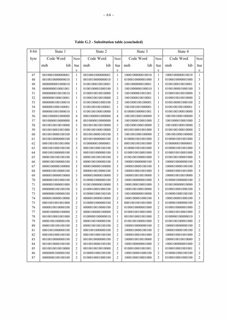
- 64 -
Table G.2 - Substitution table (concluded)
8-bit State 1 State 2 State 3 State 4
byte Code Word Next Code Word Next Code Word Next Code Word Next
msb lsb State
msb lsb State
msb lsb State
msb lsb State
47 48 49 50 51 52 53 54 55 56 57 58 59 60 61 62 63 64 65 66 67 68 69 70 71 72 73 74 75 76 77 78 79 80 81 82 83 84 85 86 87
0010001000000001 0010010000000010 0000000001000010 0000000010001001 0000000010010010 0000000100010001 0000000100100010 0000001000100001 0000001001000010 0001000001000000 0010000010000000 0010010010010000 0010010001001000 0010010000100100 0010010000000100 0001001001001000 0001001000100100 0001001000000100 0000100100100100 0000100100000100 0000100000100000 0000010010000100 0000010000010000 0000001001000100 0000001000001000 0000000100100100 0000000100000100 0000010000010000 0001001001001000 0000010010000100 0000100000100000 0010010001001000 0000100100000100 0000100100100100 0001001000000100 0001001000100100 0010010000000100 0010010000100100 0010010010010000 0000000100000100 0000000100100100
1 1 1 1 1 1 1 1 1 4 4 3 3 3 3 3 3 3 3 3 3 3 3 3 3 3 3 2 2 2 2 2 2 2 2 2 2 2 2 2 2
0010001000000001 0010010000000010 0100100010010001 0100100001000100 0100010010010000 0100010010010000 0100100001000100 0100100100100001 0100100100010000 0001000001000000 0010000010000000 0010010010010000 0100100100010000 0010010000100100 0010010000000100 0100000010000001 0001001000100100 0001001000000100 0000100100100100 0000100100000100 0000100000100000 0000010010000100 0000010000010000 0100001000000100 0100100000010000 0100010001000100 0100001000100100 0000010000010000 0100001000000100 0000010010000100 0000100000100000 0100000100000010 0000100100000100 0000100100100100 0001001000000100 0001001000100100 0010010000000100 0010010000100100 0010010010010000 0100001000100100 0100010001000100
1 1 1 3 3 2 2 1 3 4 4 3 2 3 3 1 3 3 3 3 3 3 3 2 3 3 3 2 3 2 2 1 2 2 2 2 2 2 2 2 2
1000100000010010 0100010000001000 1001000000010001 1001000000100010 1001000001001001 1001000010010001 1001000100100001 1001001001000001 0100001000001001 1001001000100000 1001000010001000 1001000100010000 0010010001001000 1001001000100000 0100001001001000 0001001001001000 0100001001001000 0100010010001000 0100100100001000 1000010000000100 1000010000100100 1000010001001000 1000010010010000 1000100000001000 1000100010001000 1000100100010000 1001000000010000 1000100001000100 0001001001001000 0100010000001000 0100010010001000 0010010001001000 0100100100001000 1000010000000100 1000010000100100 1000010001001000 1000010010010000 1000100000001000 0100010001001001 1000100001000100 1000100010001000
1 3 1 1 1 1 1 1 1 3 2 2 3 2 2 3 3 3 3 3 3 3 3 3 3 3 3 3 2 2 2 2 2 2 2 2 2 2 1 2 2
1000100000010010 0100010000001000 0100100010010001 0100100001000100 0100010010010000 0100010010010000 0100100001000100 0100100100100001 0100100100010000 1001001000100000 1001000010001000 1001000100010000 0100100100010000 1001001000100000 0100001001001000 0100000010000001 0100001001001000 0100010010001000 0100100100001000 1000010000000100 1000010000100100 1000010001001000 1000010010010000 0100001000000100 0100100000010000 0100010001000100 0100001000100100 1000100001000100 0100001000000100 0100010000001000 0100010010001000 0100000100000010 0100100100001000 1000010000000100 1000010000100100 1000010001001000 1000010010010000 1000100000001000 0100010001001001 0100001000100100 0100010001000100
1 3 1 3 3 2 2 1 3 3 2 2 2 2 2 1 3 3 3 3 3 3 3 2 3 3 3 3 3 2 2 1 2 2 2 2 2 2 1 2 2
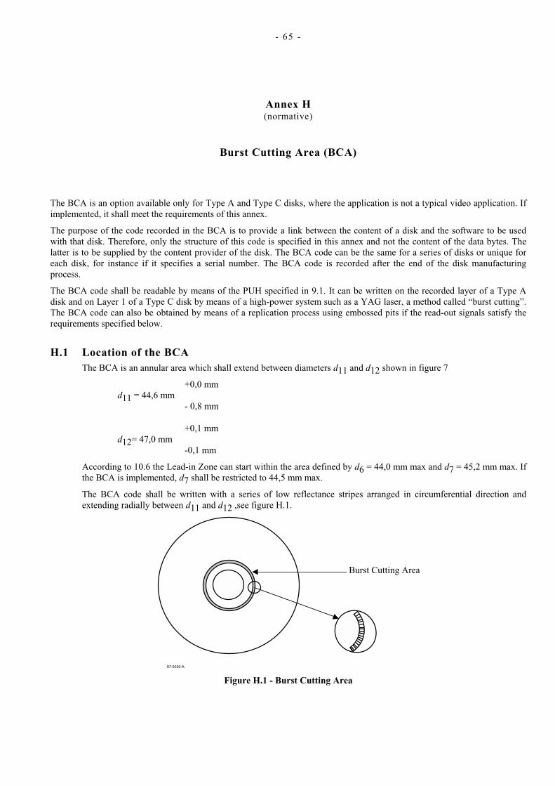
- 65 -
Annex H (normative)
Burst Cutting Area (BCA)
The BCA is an option available only for Type A and Type C disks, where the application is not a typical video application. If implemented, it shall meet the requirements of this annex.
The purpose of the code recorded in the BCA is to provide a link between the content of a disk and the software to be used with that disk. Therefore, only the structure of this code is specified in this annex and not the content of the data bytes. The latter is to be supplied by the content provider of the disk. The BCA code can be the same for a series of disks or unique for each disk, for instance if it specifies a serial number. The BCA code is recorded after the end of the disk manufacturing process.
The BCA code shall be readable by means of the PUH specified in 9.1. It can be written on the recorded layer of a Type A disk and on Layer 1 of a Type C disk by means of a high-power system such as a YAG laser, a method called “burst cutting”. The BCA code can also be obtained by means of a replication process using embossed pits if the read-out signals satisfy the requirements specified below.
H.1 Location of the BCA The BCA is an annular area which shall extend between diameters d11 and d12 shown in figure 7
+0,0 mm d11 = 44,6 mm - 0,8 mm
+0,1 mm d12= 47,0 mm -0,1 mm
According to 10.6 the Lead-in Zone can start within the area defined by d6 = 44,0 mm max and d7 = 45,2 mm max. If the BCA is implemented, d7 shall be restricted to 44,5 mm max.
The BCA code shall be written with a series of low reflectance stripes arranged in circumferential direction and extending radially between d11 and d12 ,see figure H.1.
Figure H.1 - Burst Cutting Area
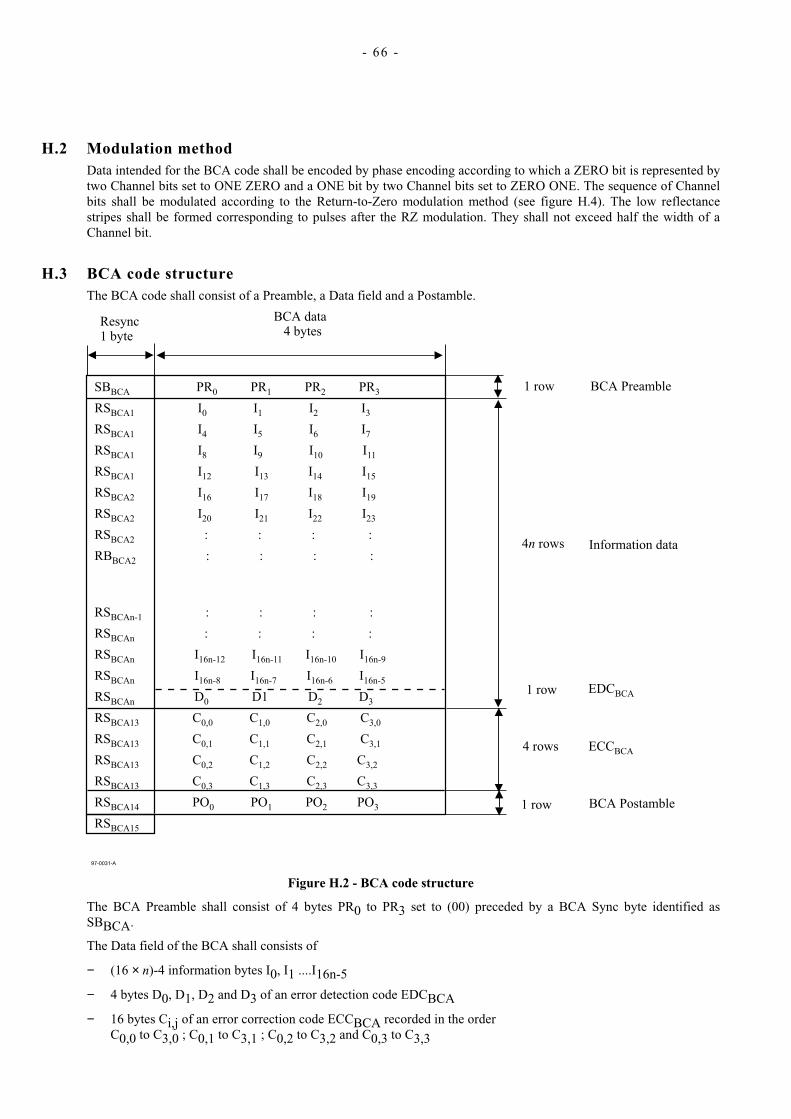
- 66 -
H.2 Modulation method Data intended for the BCA code shall be encoded by phase encoding according to which a ZERO bit is represented by two Channel bits set to ONE ZERO and a ONE bit by two Channel bits set to ZERO ONE. The sequence of Channel bits shall be modulated according to the Return-to-Zero modulation method (see figure H.4). The low reflectance stripes shall be formed corresponding to pulses after the RZ modulation. They shall not exceed half the width of a Channel bit.
H.3 BCA code structure The BCA code shall consist of a Preamble, a Data field and a Postamble.
Figure H.2 - BCA code structure
The BCA Preamble shall consist of 4 bytes PR0 to PR3 set to (00) preceded by a BCA Sync byte identified as SBBCA.
The Data field of the BCA shall consists of
− (16 × n)-4 information bytes I0, I1 ....I16n-5
− 4 bytes D0, D1, D2 and D3 of an error detection code EDCBCA
− 16 bytes Ci,j of an error correction code ECCBCA recorded in the order C0,0 to C3,0 ; C0,1 to C3,1 ; C0,2 to C3,2 and C0,3 to C3,3

- 67 -
− where n is an integer such that 1 ≤ n ≤12
− a Resync byte RSBCAi shall be inserted before each 4-byte row of Ii bytes, changing every 4th row (see figure H.3)
The BCA Postamble shall consist of 4 bytes PO0 to PO3 set to (55) and preceded by Resync byte RSBCA14 and followed by Resync byte RSBCA15.
H.4 Error Detection Code EDCBCA The 4 bytes D0 to D3 shall follow the information bytes Ii. Polynomials EDCBCA(x) and IBCA(x) shall be as follows.
31
EDCBCA(x) = ∑∑∑∑ bi xi
i = 0
128n-1
IBCA(x) = ∑∑∑∑ bi xi
i = 32
where i is the bit number starting with 0 and counted from the lsb of the last byte of EDCBCA to the msb of the first byte of information data. The value of the i-th bit is represented by bi. The polynomial EDCBCA(x) shall be calculated as follows
EDCBCA(x) = IBCA(x) mod G(x)
where G(x) = x32 + x31 + x4 + 1
H.5 BCA Error Correction Code ECCBCA A Reed-Solomon ECC code with a 4-way interleave shall be applied to the information data and the EDCBCA Polynomials RBCAj(x) and IBCAj(x) shall be as follows.
3
RBCAj(x) = ∑∑∑∑ Cj,i x3-i
i = 0
4n-2
IBCAj(x) = ∑∑∑∑ I(j+4i) x51-i + Dj x
52-4n i = 0
Where Im represents the m-th information data byte and Dk represents the k-th EDCBCA byte.
The polynomial RBCAj(x) shall be calculated as follows:
RBCAj(x) = IBCAj(x) mod GpBCA(x)
3
GpBCA(x) = ΠΠΠΠ ( x + αk ) k = 0
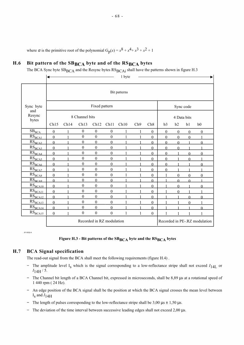
- 68 -
where α is the primitive root of the polynomial Gp(x) = x8 + x4+ x3 + x2 + 1
H.6 Bit pattern of the SBBCA byte and of the RSBCA bytes The BCA Sync byte SBBCA and the Resync bytes RSBCAi shall have the patterns shown in figure H.3
Figure H.3 - Bit patterns of the SBBCA byte and the RSBCA bytes
H.7 BCA Signal specification The read-out signal from the BCA shall meet the following requirements (figure H.4) .
− The amplitude level Is which is the signal corresponding to a low-reflectance stripe shall not exceed I14L or I14H / 5.
− The Channel bit length of a BCA Channel bit, expressed in microseconds, shall be 8,89 µs at a rotational speed of 1 440 rpm ( 24 Hz).
− An edge position of the BCA signal shall be the position at which the BCA signal crosses the mean level between Is and I14H
− The length of pulses corresponding to the low-reflectance stripe shall be 3,00 µs ± 1,50 µs.
− The deviation of the time interval between successive leading edges shall not exceed 2,00 µs.
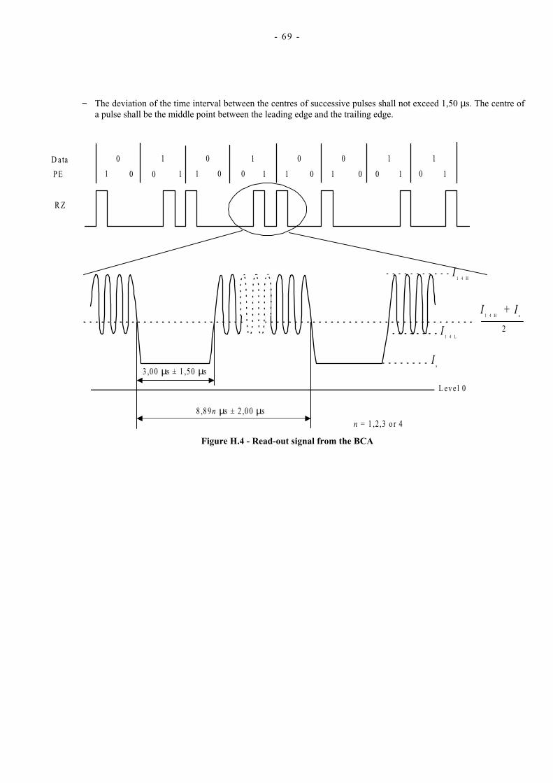
- 69 -
− The deviation of the time interval between the centres of successive pulses shall not exceed 1,50 µs. The centre of a pulse shall be the middle point between the leading edge and the trailing edge.
8 ,8 9 s ± 2 ,0 0 sn µ µn = 1 ,2 ,3 o r 4
L ev e l 0
2
I1 4 H
I1 4 L
Is
I I1 4 H s
+
3 ,0 0 s ± 1 ,50 sµ µ
P E
R Z
D a ta
1
0
0 0
0
0 0
0
0
0
0 0 0
1
1 1
1
1 1 1
1
1
1
1
Figure H.4 - Read-out signal from the BCA

- 70 -

- 71 -
Annex J
(normative)
Source Identification Code (SID)
J.1 General The requirements of this annex apply only to DVD-Read-Only disks using the DVD Audio Format.
The Source Identification Code (SID) shall be recorded on the inner side of the disk. It shall consist of visible characters such as the Registered Mark (™), a registered number of a laser beam recorder or a registered number of the mould by means of which the disk has been produced.
The SID Code shall consist of two elements : The Mastering Code and the Mould Code. The Mastering Code shall be generated by using the Laser Beam Recorder (LBR), thus it exist on the stamper. The Mould Code shall be etched on a mould, preferably on the mirror block. When a substrate is replicated, the Mastering Code shall be recorded on the side of the substrate on which the embossed data pits are recorded, and the Mould Code shall be recorded on the other side of the substrate. This annex specifies the area for the mandatory SID Code as well as an additional area in which other characters may be recorded, for instance the name of the manufacturer of the disk.
J.2 Requirement for implementation The requirements of this annex apply only to DVD - Read-Only disks using the DVD Audio Format. The implementation of this annex is optional. If implemented all requirements of this annex are mandatory.
J.3 Recommendation It is recommended to record the SID Code also on DVD-Read-Only disks other than those used in audio applications.
J.4 Mastering Code J.4.1 Location
The Mastering Code shall be recorded within a zone delimited by a maximum radius of 22,5 mm. It shall be in an area where the reflecting layer exists. If the BCA option (See annex H) is implemented, the position of the Mastering Code shall be shifted toward the centre of the disk so that it does not overlap with the BCA.
J.4.2 Legibility The height of the Mastering Code shall be 0,5 mm min. It shall be legible without magnification. It shall be readable from right to left when seen from the entrance surface of the disk. The position of the stack ring shall be chosen so as not to be over the Mastering Code.
J.4.3 Structure and space allocation The area in which the Mastering Code is recorded shall be divided into two parts (Figure J.1).
In the first one either the characters of the International Federation of Photographic Industry (IFPI) in capital letter or the logo of IFPI shall be recorded.
In the second part of this area the LBR identification shall be recorded as a 4-character alpha-numeric identifier.
The area in which the Mastering Code shall be recorded shall consist of an arc of 30° max. The Mastering Code shall be clearly separated from other characters.
A further arc of 30° shall be reserved for future use.
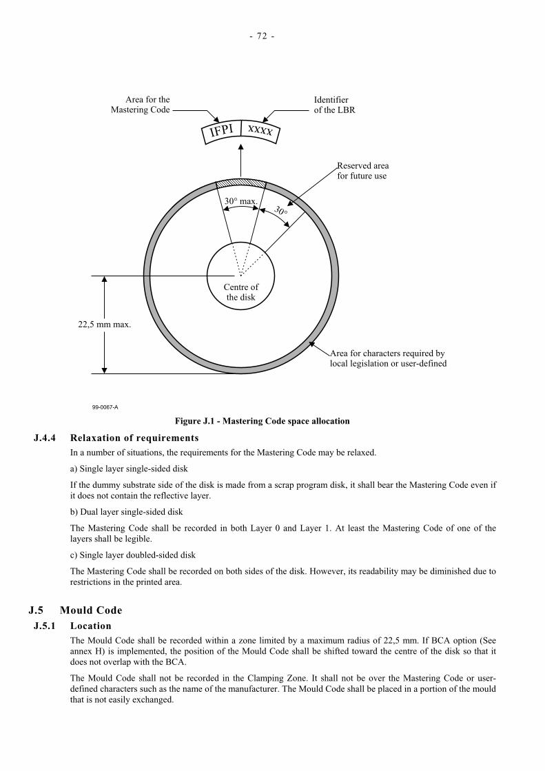
- 72 -
xxxx
IFPI
30°
30° max.
Centre ofthe disk
Reserved areafor future use
Area for characters required bylocal legislation or user-defined
Area for theMastering Code
Identifierof the LBR
22,5 mm max.
99-0067-A
Figure J.1 - Mastering Code space allocation
J.4.4 Relaxation of requirements In a number of situations, the requirements for the Mastering Code may be relaxed.
a) Single layer single-sided disk
If the dummy substrate side of the disk is made from a scrap program disk, it shall bear the Mastering Code even if it does not contain the reflective layer.
b) Dual layer single-sided disk
The Mastering Code shall be recorded in both Layer 0 and Layer 1. At least the Mastering Code of one of the layers shall be legible.
c) Single layer doubled-sided disk
The Mastering Code shall be recorded on both sides of the disk. However, its readability may be diminished due to restrictions in the printed area.
J.5 Mould Code J.5.1 Location
The Mould Code shall be recorded within a zone limited by a maximum radius of 22,5 mm. If BCA option (See annex H) is implemented, the position of the Mould Code shall be shifted toward the centre of the disk so that it does not overlap with the BCA.
The Mould Code shall not be recorded in the Clamping Zone. It shall not be over the Mastering Code or user-defined characters such as the name of the manufacturer. The Mould Code shall be placed in a portion of the mould that is not easily exchanged.
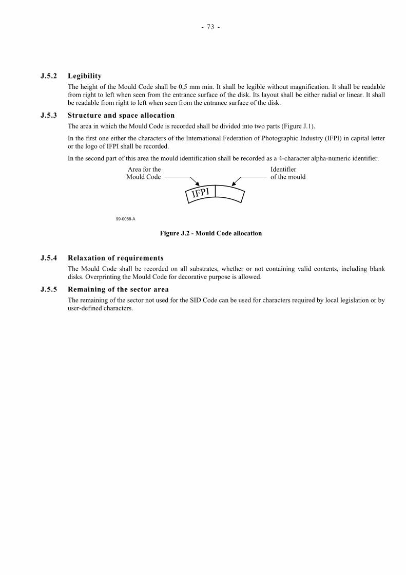
- 73 -
J.5.2 Legibility The height of the Mould Code shall be 0,5 mm min. It shall be legible without magnification. It shall be readable from right to left when seen from the entrance surface of the disk. Its layout shall be either radial or linear. It shall be readable from right to left when seen from the entrance surface of the disk.
J.5.3 Structure and space allocation The area in which the Mould Code is recorded shall be divided into two parts (Figure J.1).
In the first one either the characters of the International Federation of Photographic Industry (IFPI) in capital letter or the logo of IFPI shall be recorded.
In the second part of this area the mould identification shall be recorded as a 4-character alpha-numeric identifier.
IFPI
Area for theMould Code
Identifierof the mould
99-0068-A
Figure J.2 - Mould Code allocation
J.5.4 Relaxation of requirements The Mould Code shall be recorded on all substrates, whether or not containing valid contents, including blank disks. Overprinting the Mould Code for decorative purpose is allowed.
J.5.5 Remaining of the sector area The remaining of the sector not used for the SID Code can be used for characters required by local legislation or by user-defined characters.

- 74 -
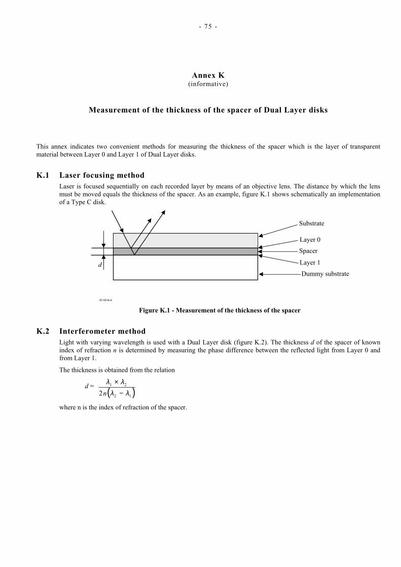
- 75 -
Annex K (informative)
Measurement of the thickness of the spacer of Dual Layer disks
This annex indicates two convenient methods for measuring the thickness of the spacer which is the layer of transparent material between Layer 0 and Layer 1 of Dual Layer disks.
K.1 Laser focusing method Laser is focused sequentially on each recorded layer by means of an objective lens. The distance by which the lens must be moved equals the thickness of the spacer. As an example, figure K.1 shows schematically an implementation of a Type C disk.
Figure K.1 - Measurement of the thickness of the spacer
K.2 Interferometer method Light with varying wavelength is used with a Dual Layer disk (figure K.2). The thickness d of the spacer of known index of refraction n is determined by measuring the phase difference between the reflected light from Layer 0 and from Layer 1.
The thickness is obtained from the relation
d = ( )λ λ
λ λ1 2
2 12
×−n
where n is the index of refraction of the spacer.
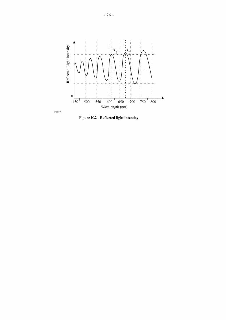
- 76 -
Figure K.2 - Reflected light intensity

- 77 -
Annex L (informative)
Note on the Reference Code
The purpose of the Reference Code is to provide Channel bit patterns that generates (3T-6T-7T) separating signals. A drive may use these signals to adjust the equalizer for reading HF signals. This annex describes a practical method for generating the required Channel bit patterns.
As described in Section 4, Main Data is scrambled before generating ECC bytes. In order to get, after scrambling and ECC bytes generation but just before modulation, a specific data pattern that will generate 3T, 6T and 7T modulated channel signals, pre-scrambling is applied to the Main Data. If the pre-scrambling data is the same as the normal scrambling data used by the encoding process described in this ECMA Standard, then the same scrambling data is added twice to the user data and non-scrambled data appears just before generating the ECC bytes. This means that the Recording Frames contain fixed data patterns which are duplicates of the Main Data, except for the ECC bytes. The pre-scrambling data is added to all 32 Data Frames used in the Reference Code Zone, except to the first 160 Main Data bytes of the first Data Frame in each ECC Block, so as to avoid large DSV values.
The following steps show how to process the Main Data intended for the Reference Code before it is fed into the encoding system.
Step 1
Set all Main Data bytes of the 32 Data Frames to (AC).
Step2
This step is applied to the Data Frames intended for Physical Sectors with Sector Numbers 192 512, (02F000) to 192 543, (02F01F).
To Physical Sectors with Sector Numbers from 192 512 (02F000) to 192 527 (02F00F) add the pre-scrambling data, generated using the scrambling procedure of clause 17 with the initial pre-set number (0) to all Main Data bytes, except the first 160 of the Physical Sector with Sector Number 192 512, (02F000).
To Physical Sectors with Sector Numbers from 192 528, (02F010) to 192 543, (02F01F) add the pre-scrambling data, generated using the scrambling procedure of clause 17 with the initial pre-set number (1), to all Main Data bytes, except the first 160 such bytes of the Physical Sector with Sector Number 192 528, (02F010).

- 78 -
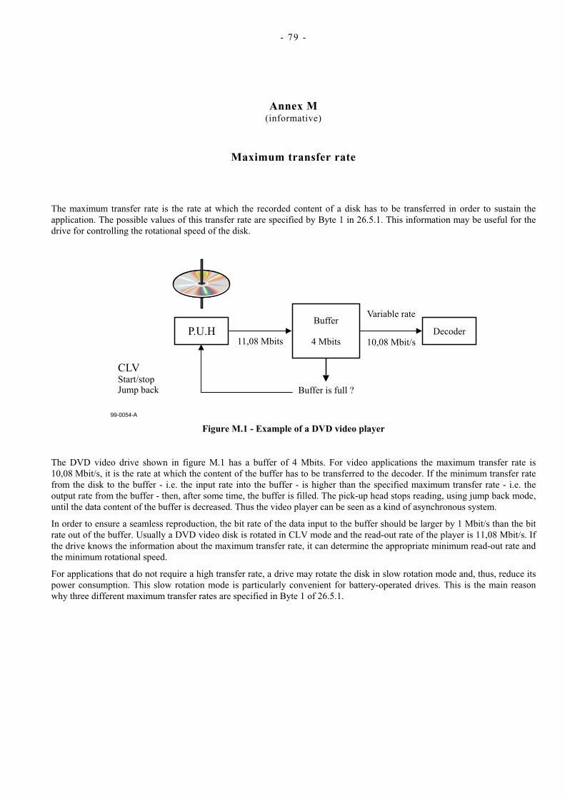
- 79 -
Annex M (informative)
Maximum transfer rate
The maximum transfer rate is the rate at which the recorded content of a disk has to be transferred in order to sustain the application. The possible values of this transfer rate are specified by Byte 1 in 26.5.1. This information may be useful for the drive for controlling the rotational speed of the disk.
P.U.HBuffer
4 MbitsDecoder
Buffer is full ?
11,08 Mbits 10,08 Mbit/s
Variable rate
CLVStart/stopJump back
99-0054-A
Figure M.1 - Example of a DVD video player
The DVD video drive shown in figure M.1 has a buffer of 4 Mbits. For video applications the maximum transfer rate is 10,08 Mbit/s, it is the rate at which the content of the buffer has to be transferred to the decoder. If the minimum transfer rate from the disk to the buffer - i.e. the input rate into the buffer - is higher than the specified maximum transfer rate - i.e. the output rate from the buffer - then, after some time, the buffer is filled. The pick-up head stops reading, using jump back mode, until the data content of the buffer is decreased. Thus the video player can be seen as a kind of asynchronous system.
In order to ensure a seamless reproduction, the bit rate of the data input to the buffer should be larger by 1 Mbit/s than the bit rate out of the buffer. Usually a DVD video disk is rotated in CLV mode and the read-out rate of the player is 11,08 Mbit/s. If the drive knows the information about the maximum transfer rate, it can determine the appropriate minimum read-out rate and the minimum rotational speed.
For applications that do not require a high transfer rate, a drive may rotate the disk in slow rotation mode and, thus, reduce its power consumption. This slow rotation mode is particularly convenient for battery-operated drives. This is the main reason why three different maximum transfer rates are specified in Byte 1 of 26.5.1.

- 80 -
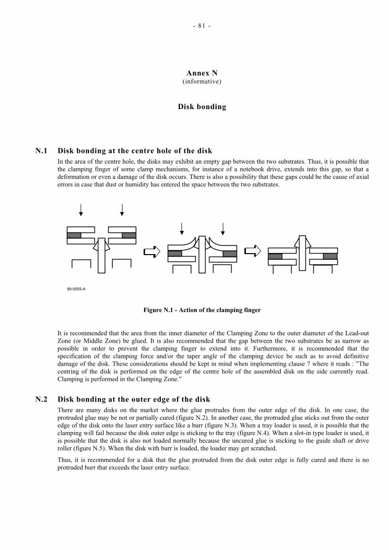
- 81 -
Annex N (informative)
Disk bonding
N.1 Disk bonding at the centre hole of the disk In the area of the centre hole, the disks may exhibit an empty gap between the two substrates. Thus, it is possible that the clamping finger of some clamp mechanisms, for instance of a notebook drive, extends into this gap, so that a deformation or even a damage of the disk occurs. There is also a possibility that these gaps could be the cause of axial errors in case that dust or humidity has entered the space between the two substrates.
99-0055-A
Figure N.1 - Action of the clamping finger
It is recommended that the area from the inner diameter of the Clamping Zone to the outer diameter of the Lead-out Zone (or Middle Zone) be glued. It is also recommended that the gap between the two substrates be as narrow as possible in order to prevent the clamping finger to extend into it. Furthermore, it is recommended that the specification of the clamping force and/or the taper angle of the clamping device be such as to avoid definitive damage of the disk. These considerations should be kept in mind when implementing clause 7 where it reads : ”The centring of the disk is performed on the edge of the centre hole of the assembled disk on the side currently read. Clamping is performed in the Clamping Zone.”
N.2 Disk bonding at the outer edge of the disk There are many disks on the market where the glue protrudes from the outer edge of the disk. In one case, the protruded glue may be not or partially cured (figure N.2). In another case, the protruded glue sticks out from the outer edge of the disk onto the laser entry surface like a burr (figure N.3). When a tray loader is used, it is possible that the clamping will fail because the disk outer edge is sticking to the tray (figure N.4). When a slot-in type loader is used, it is possible that the disk is also not loaded normally because the uncured glue is sticking to the guide shaft or drive roller (figure N.5). When the disk with burr is loaded, the loader may get scratched.
Thus, it is recommended for a disk that the glue protruded from the disk outer edge is fully cured and there is no protruded burr that exceeds the laser entry surface.
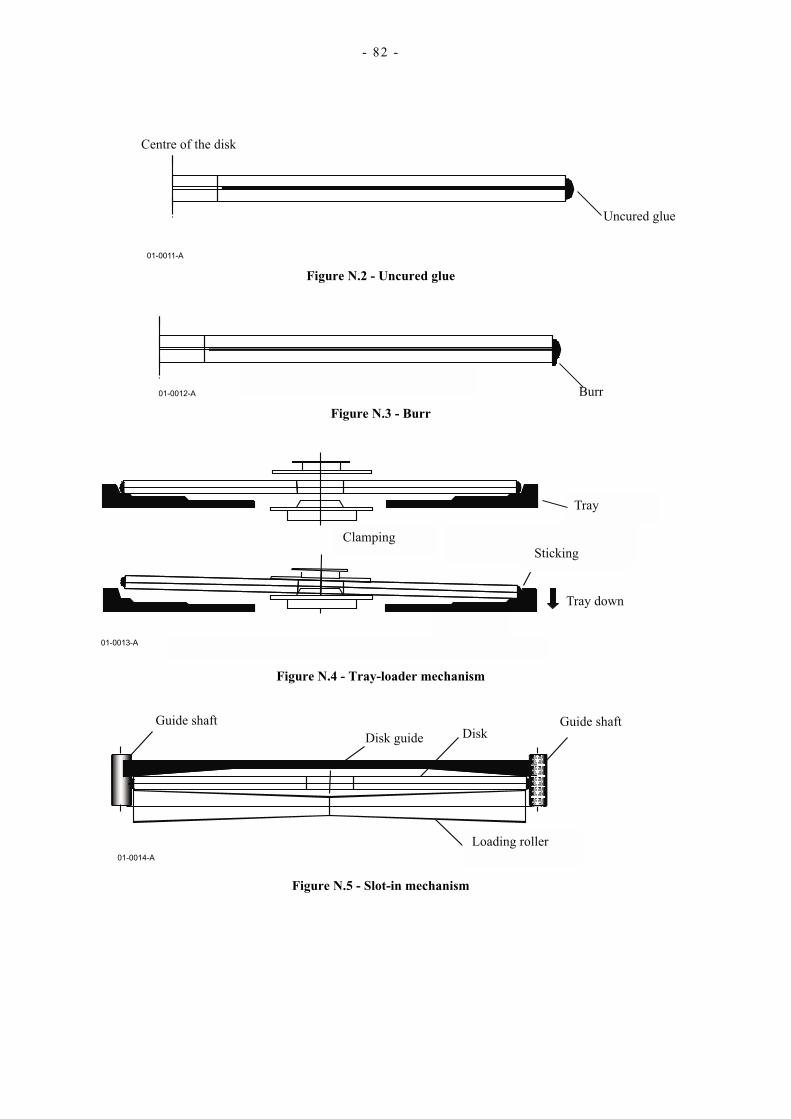
- 82 -
Figure N.2 - Uncured glue
Figure N.3 - Burr
Figure N.4 - Tray-loader mechanism
Figure N.5 - Slot-in mechanism

- 83 -
Annex P (informative)
Transportation
P.1 General As transportation occurs under a wide range of temperature and humidity variations, for differing periods, by many methods of transport and in all parts of the world, it is not possible to specify mandatory conditions for transportation or for packaging.
P.2 Packaging The form of packaging should be agreed between sender and recipient or, in absence of such an agreement, is the responsibility of the sender. It should take into account the following hazards.
P.2.1 Temperature and humidity Insulation and wrapping should be designed to maintain the conditions for storage over the estimated period of transportation.
P.2.2 Impact loads and vibrations a) Avoid mechanical loads that would distort the shape of the disk.
b) Avoid dropping the disk.
c) Disks should be packed in a rigid box containing adequate shock-absorbent material.
d) The final box should have a clean interior and a construction that provides sealing to prevent the ingress of dirt and moisture.


..
Free printed copies can be ordered from:
ECMA 114 Rue du Rhône CH-1204 Geneva Switzerland
Fax: +41 22 849.60.01 Internet: [email protected]
Files of this Standard can be freely downloaded from the ECMA web site (www.ecma.ch). This site gives full information on ECMA, ECMA activities, ECMA Standards and Technical Reports.

ECMA
114 Rue du Rhône CH-1204 Geneva Switzerland
See inside cover page for obtaining further soft or hard copies.