12 Multiprobe SPM - Hasegawa Group Entrance · 12 Multiprobe SPM Shuji Hasegawa 12.1 Present Status...
6
12 Multiprobe SPM Shuji Hasegawa 12.1 Present Status The multiprobe scanning probe microscope (SPM), in which several tips or cantilevers are independently driven and arranged in arbitrary configurations on samples surfaces, has recently attracted considerable attention as a very versatile tool for electrical characterization at nanometer scales. The SPM tips/probes are employed as current sources, voltage pick-up probes, and field- gate electrodes as well as tweezers for structure manipulations. Several groups are developing different types of multiprobe SPMs [1–7], and some companies begin to deliver the products [8]. These commercial machines are mainly for testing electrical characteristics of nanometer-scale electronic devices, and re- garded as a tool evolved from conventional electrical probers. Some of them are for electrical measurements of biological cells and proteins. In order to control the contact pressure between the probes and sample surfaces, many of them have ability of atomic force microscopy not only for imaging, but also for electrical measurements with conductive cantilevers. But they do not nec- essarily have atomic resolutions, and control precision of tip/probe positions is poorer than 10 nm. The apparatus and operation system are not yet fully developed, and still have much room for evolution in many aspects. Especially the operation system for controlling the multiprobes with atomic precisions as an organic whole is still lacking, and therefore it seems that the true value of multiprobe SPM is not yet realized. Figure 12.1a shows a schematic of the four-tip scanning tunneling micro- scope (STM) apparatus in an ultrahigh vacuum (UHV) chamber developed at the University of Tokyo, and Fig.12.1b shows a photograph of the goniometer stage on which the sample and four sets of scanners are mounted [9,10]. The four tips of STM are driven independently under scanning electron micro- scope (SEM) for positioning the tips precisely with arbitrary arrangements on specified areas on the sample surface. Each tip points to the sample at the center with 45 ◦ from the sample surface, and is driven by a special type of a piezo-scanner for fine positioning and by three sets of piezo-actuators
Transcript of 12 Multiprobe SPM - Hasegawa Group Entrance · 12 Multiprobe SPM Shuji Hasegawa 12.1 Present Status...

12
Multiprobe SPM
Shuji Hasegawa
12.1 Present Status
The multiprobe scanning probe microscope (SPM), in which several tips orcantilevers are independently driven and arranged in arbitrary configurationson samples surfaces, has recently attracted considerable attention as a veryversatile tool for electrical characterization at nanometer scales. The SPMtips/probes are employed as current sources, voltage pick-up probes, and field-gate electrodes as well as tweezers for structure manipulations. Several groupsare developing different types of multiprobe SPMs [1–7], and some companiesbegin to deliver the products [8]. These commercial machines are mainly fortesting electrical characteristics of nanometer-scale electronic devices, and re-garded as a tool evolved from conventional electrical probers. Some of themare for electrical measurements of biological cells and proteins. In order tocontrol the contact pressure between the probes and sample surfaces, manyof them have ability of atomic force microscopy not only for imaging, but alsofor electrical measurements with conductive cantilevers. But they do not nec-essarily have atomic resolutions, and control precision of tip/probe positionsis poorer than 10 nm. The apparatus and operation system are not yet fullydeveloped, and still have much room for evolution in many aspects. Especiallythe operation system for controlling the multiprobes with atomic precisionsas an organic whole is still lacking, and therefore it seems that the true valueof multiprobe SPM is not yet realized.
Figure 12.1a shows a schematic of the four-tip scanning tunneling micro-scope (STM) apparatus in an ultrahigh vacuum (UHV) chamber developed atthe University of Tokyo, and Fig. 12.1b shows a photograph of the goniometerstage on which the sample and four sets of scanners are mounted [9,10]. Thefour tips of STM are driven independently under scanning electron micro-scope (SEM) for positioning the tips precisely with arbitrary arrangementson specified areas on the sample surface. Each tip points to the sample atthe center with 45◦ from the sample surface, and is driven by a special typeof a piezo-scanner for fine positioning and by three sets of piezo-actuators
shuji
ハイライト表示
shuji
ハイライト表示
shuji
ハイライト表示
shuji
ハイライト表示

96 S. Hasegawa
(a)
FE GUN
#1
#2
#3 #4
Field-EmissionScanningElectronMicroscope
SecondaryElectronDetector
4 Sets ofSTMScanners
GoniometerStage
Evaporator
RHEED
(b)
Fig. 12.1. (a) Schematics of the independently driven four-tip STM, installed inan UHV-SEM-RHEED system. (b) A photograph of the goniometer stage on whicha sample and the four-tip scanners are mounted under the SEM column [9,10]
(Microslide, Omicron) for coarse motion. The goniometer stage enables paral-lel shifts in three directions and tilt rotation with respect to the SEM electronbeam. The sample can be rotated azimuthally by 360◦ with respect to thestage. These positioning mechanisms enable fine adjustments with respect tothe SEM electron beam, required to perform reflection-high-energy electrondiffraction (RHEED) and scanning reflection electron microscopy (SREM) ob-servations of the sample surface simultaneously. These supplementary electronmicroscopy/diffraction techniques are indispensable not only for positioningthe four tips properly, but also for confirming the surface structures of sample.The STM tips and sample can be exchanged and installed by transfer rodsfrom load-lock chambers without breaking vacuum.
This apparatus enables usual STM operation by each tip independently,and also four-point probe (4PP) conductivity measurements with variousprobe arrangements and spacing. The four tips approach the sample sur-face simultaneously with feedback control by tunnel-current detection. Afterthat, the tips are brought into direct contacts with the sample surface, andthen the 4PP conductivity measurement is performed. The preamplifier isswitched from the tunnel-current mode to the 4PP conductivity measure-ment mode. Control system for the four-tip STM is still in its infancy. Eachtip is independently controlled, but not in an integrated way. If the positionsof all tips are controlled by their xyz coordinates at nanometer-scale precisionby a single controller, we do not need SEM for tip positioning anymore. Amethod for navigating two STM tips is developed by using a special type ofsample [11].
shuji
ハイライト表示

12 Multiprobe SPM 97
(a)
200 m m
(b)
Fig. 12.2. (a) SEM images of the four W tips in the four-tip STM [9]. (b) The fourtips contacting a Co-silicide nanowire on an Si(110) surface [12]
Figure 12.2a shows an SEM image of four tungsten tips in the four-tipSTM [9, 12]. The probe spacing can be changed from ca. 100 nm to 1mm,and arranged in arbitrary ways such as in linear or in a square with equidis-tant probe spacings [13]. These four tips are used for the 4PP conductivitymeasurements of microscopic regions and objects. When the probe spacing isreduced on the order of microns, we can measure the electrical conductivitythrough the topmost atomic layers on a crystal with high sensitivity [14, 15]as well as individual microscopic objects such as nanowires [12]. When thefour tips are arranged in a square on a sample surface, we can measure theanisotropy of conductivity [13].
12.1.1 Improvements
The following two issues should be improved from technical points of view inorder to make the multiprobe SPM a more versatile tool for nanometer-scalemeasurements.
1. Control system. Many of the multiprobe SPMs need an auxiliary micro-scope such as SEM and optical microscope to observe and position thetips/probes in the designed arrangements on a sample surface. And inmany cases the tips/probes are independently driven with separate setsof controllers without mutual communication. These make the operationvery troublesome. Therefore, a user-friendly controller, by which the mul-tiprobes are controlled with nanometer precisions in integrated ways bya single computer, is highly desired. Furthermore, it becomes much moreconvenient if we can control each tip by its xyz coordinates. For thispurpose, we need a so-called closed-loop system in which the probe move-ments driven by scanners are simultaneously measured by some kinds ofdisplacement sensors, and the results are used for feedback of tip po-sitioning. Such a controller is recently produced experimentally, whilethe tip-positioning precision is not yet enough for the nanometer-scalemeasurements.
98 S. Hasegawa
50nm
500nm 300nm
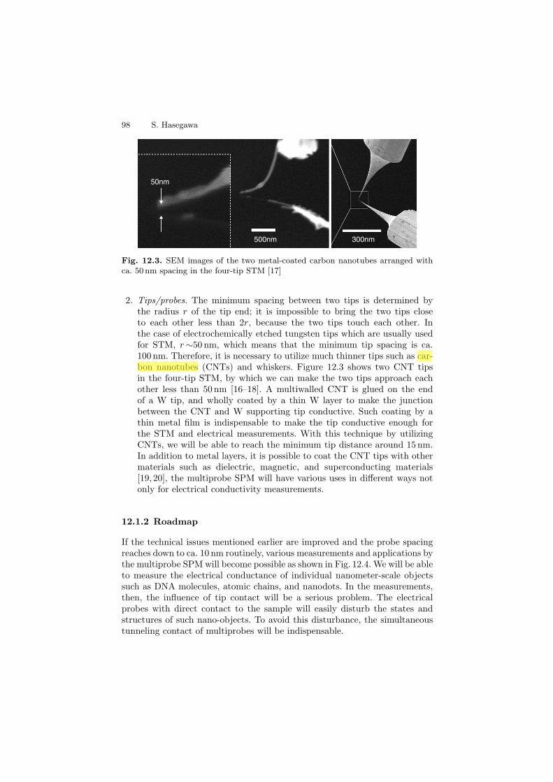
Fig. 12.3. SEM images of the two metal-coated carbon nanotubes arranged withca. 50 nm spacing in the four-tip STM [17]
2. Tips/probes. The minimum spacing between two tips is determined bythe radius r of the tip end; it is impossible to bring the two tips closeto each other less than 2r, because the two tips touch each other. Inthe case of electrochemically etched tungsten tips which are usually usedfor STM, r∼50 nm, which means that the minimum tip spacing is ca.100 nm. Therefore, it is necessary to utilize much thinner tips such as car-bon nanotubes (CNTs) and whiskers. Figure 12.3 shows two CNT tipsin the four-tip STM, by which we can make the two tips approach eachother less than 50 nm [16–18]. A multiwalled CNT is glued on the endof a W tip, and wholly coated by a thin W layer to make the junctionbetween the CNT and W supporting tip conductive. Such coating by athin metal film is indispensable to make the tip conductive enough forthe STM and electrical measurements. With this technique by utilizingCNTs, we will be able to reach the minimum tip distance around 15 nm.In addition to metal layers, it is possible to coat the CNT tips with othermaterials such as dielectric, magnetic, and superconducting materials[19, 20], the multiprobe SPM will have various uses in different ways notonly for electrical conductivity measurements.
12.1.2 Roadmap
If the technical issues mentioned earlier are improved and the probe spacingreaches down to ca. 10 nm routinely, various measurements and applications bythe multiprobe SPM will become possible as shown in Fig. 12.4. We will be ableto measure the electrical conductance of individual nanometer-scale objectssuch as DNA molecules, atomic chains, and nanodots. In the measurements,then, the influence of tip contact will be a serious problem. The electricalprobes with direct contact to the sample will easily disturb the states andstructures of such nano-objects. To avoid this disturbance, the simultaneoustunneling contact of multiprobes will be indispensable.
shuji
ハイライト表示

12 Multiprobe SPM 99
20052000 2010 2015
Probe Spacing
10 nm
100 nm
1 µm2004 Conductance of Nanowires/Nanotubes
2006 Conductivity of SingleTerrace/Domain/Dot
2007 Nano-Devices
2007Single AtomStrand/DNA
2006 Mapping of Green’s Function
2005 Nanotube Tips for Multi-Probes
2010 Atom Manipulationwith Multi-Probes
2000 IndependentControl of Multi-Probes
2006 Organic Control of Multi-probes
2010 QuantumEntanglement
1 nm
2001 MonolayerConductivity
2005 Micro-Devices
2012 Elements ofQuantum Computers
Done
Will be done
Uncertain
Year
10 µm
Fig. 12.4. Future prospect about the multiprobe SPM
When the tip spacing is comparable to the coherence length of carriers inthe sample, a new type of measurement, i.e., real-space mapping of Green’sfunction, will be possible by the multitip STM [21,22]. This “Green’s functionSTM” measures the change of tunneling current through a tip during changingthe tunneling bias voltages of other tips. Such nonlocal phenomena includingelectron correlation effects can be measured when the tips are brought closeto each other in a range of carrier coherence length. With this new type ofmultiprobe SPM, it will be possible to measure quantum entangled states innanostructures which will be useful as elements of quantum computers.
The multiprobe SPM will be also utilized for structural modificationsand atomic/molecular manipulations. With use of multiprobes, such structureconstructions and characterizations will be simultaneously possible.
References
1. S. Tsukamoto, B. Siu, N. Nakagiri, Rev. Sci. Instrum. 62, 1767 (1991)2. M. Aono, C.-S. Jiang, T. Nakayama, T. Okuda, S. Qiao, M. Sakurai,
C. Thirstrup, Z.-H. Wu, J. Surf. Sci. Soc. Jpn. 19, 698 (1998), in Japanese3. H. Okamoto, D.M. Chen, Rev. Sci. Instr. 72, 4398 (2001)4. H. Grube, B.C. Harrison, J. Jia, J.J. Boland, Rev. Sci. Instr. 72, 4388 (2001);
Rev. Sci. Instr. 73, 1343 (2002) [ERRATA]5. H. Watanabe, C. Manabe, T. Shigematsu, M. Shimizu: Appl. Phys. Lett. 78,
2928 (2001); 79, 2462 (2001)
shuji
ハイライト表示

100 S. Hasegawa
6. K. Takami, M. Akai-Kasaya, A. Saito, M. Aono, Y. Kuwahara, Jpn. J. Appl.Phys. 44, L120 (2005)
7. M. Ishikawa, M. Yoshimura, K. Ueda, Jpn. J. Appl. Phys. 44, 1502 (2005)8. Omicron NanoTechnology GmbH (http://www.omicron.de/), MultiProbe, Inc
(http://www.multiprobe.com/), Zyvex Co. (http://www.zyvex.com/)9. I. Shiraki, F. Tanabe, R. Hobara, T. Nagao, S. Hasegawa, Surf. Sci. 493, 643
(2001)10. S. Hasegawa, I. Shiraki, F. Tanabe, R. Hobara, Current Appl. Phys. 2, 465
(2002)11. H. Okamoto, D.M. Chen, J. Vac. Sci. Technol. A 19, 1822 (2001)12. H. Okino, I. Matsuda, R. Hobara, Y. Hosomura, S. Hasegawa, P.A. Bennett,
Appl. Phys. Lett. 86, 233108 (2005)13. T. Kanagawa, R. Hobara, I. Matsuda, T. Tanikawa, A. Natori, S. Hasegawa,
Phys. Rev. Lett. 91, 036805 (2003)14. S. Hasegawa, I. Shiraki, F. Tanabe, R. Hobara, T. Kanagawa, T. Tanikawa,
I. Matsuda, C.L. Petersen, T.M. Hansen, P. Boggild, F. Grey, Surf. Rev. Lett.10, 963 (2003)
15. S. Hasegawa, I. Shiraki, T. Tanikawa, C.L. Petersen, T.M. Hansen, P. Goggild,F. Grey, J. Phys.: Cond. Matters 14, 8379 (2002)
16. T. Ikuno, M. Katayama, M. Kishida, K. Kamada, Y. Murata, T. Yasuda,S. Honda, J. Lee, H. Mori, K. Oura, Jpn. J. Appl. Phys. 43, L644 (2004)
17. Y. Murata, S. Yoshimoto, M. Kishida, D. Maeda, T. Yasuda, T. Ikuno,S. Honda, H. Okada, R. Hobara, I. Matasuda, S. Hasegawa, K. Oura,M. Katayama, Jpn. J. Appl. Phys. 44, 5336 (2005)
18. S. Yoshimoto, Y. Murata, R. Hobara, I. Matsuda, M. Kishida, H. Konishi,T. Ikuno, D. Maeda, T. Yasuda, S. Honda, H. Okada, K. Oura, M. Katayama,S. Hasegawa, Jpn. J. Appl. Phys. 44, L1563 (2005)
19. M. Kishida, H. Konishi, Y. Murata, D. Maeda, T. Yasuda, T. Ikuno, S. Honda,M. Katayama, S. Yoshimoto, R. Hobara, I. Matsuda, S. Hasegawa, e-J. Surf.Sci. Nanotech. 3, 417 (2005)
20. T. Ikuno, T. Yasuda, S. Honda, K. Oura, M. Katayama, J.-G. Lee, H. Mori, J.Appl. Phys. 98, 114305 (2005)
21. Q. Niu, M.C. Chang, C.K. Shih, Phys. Rev. B 51, 5502 (1995)22. J.M. Byers M.E. Flatte: Phys. Rev. Lett. 74, 306 (1995)