11B-3 Performance Breakthrough in NOR Flash Memory with Dopant
2
222 978-4-86348-009-4 2009 Symposium on VLSI Technology Digest of Technical Papers 11B-3 Performance Breakthrough in NOR Flash Memory with Dopant-Segregated Schottky-Barrier (DSSB) SONOS Devices Sung-Jin Choi 1 , Jin-Woo Han 1 , Sungho Kim 1 , Dong-Il Moon 1 , Moon-Gyu Jang 2 , Jin Su Kim 3 , Kwang Hee Kim 3 , Gi Sung Lee 3 , Jae Sub Oh 3 , Myong Ho Song 3 , Yun Chang Park 3 , Jeoung Woo Kim 3 , and Yang-Kyu Choi 1 1 EECS, KAIST, Daejeon, Korea, 2 ETRI, Daejeon, Korea, 3 National Nanofab Center, Daejeon, Korea Email: [email protected] , Phone: +82-42-350-3477, Fax: +82-42-350-8565 ABSTRACT A novel dopant segregated Schottky barrier (DSSB) SONOS device as a form of double-gate (DG) is demonstrated for NOR Flash memory applications. The DSSB also applies to all-around-gate (AAG) SONOS devices. The source side injection caused by sharp energy band bending in the DSSB device results in a high-speed programming (V th shift of 4.2V @ 320ns) at a low program bias (V gs /V ds =7V/3V). Moreover, faster program speed in a narrower fin width (W fin ) due to its low parasitic resistance and enhanced gate controllability is achieved. Drain disturbance-free characteristics in a programmed cell are confirmed as well. INTRODUCTION The most critical limit is the gate length scaling in a NOR Flash memory cell, which uses a program method known as channel hot electron injection (CHEI). This method aggravates immunity against punchthrough by making drain voltage high enough to trigger a CHEI. In addition, the low injection efficiency of the hot electrons generated at the drain side and the high parasitic resistance at the source and drain (S/D) also impose a constraint on scaling the cell size down. Consequently, the lower effective program voltage due to the high parasitic S/D resistance in an extremely scaled cell results in a small V th window and thereafter retards the program speed. Our previous works focused only on a NAND Flash memory cell that utilized the DG DSSB SONOS structure [1]. It improved the programming speed as well as the short-channel effects through lower program bias. In this work, an intensive analysis of NOR Flash memory, where a similar DG and highly scaled AAG DSSB SONOS devices are employed, is carried out for the first time. It boosts the program speed even at a low program bias owing to the improved CHEI, which is enabled by the inherent sharp band bending of the DSSB at the source side. The DSSB structure provides several benefits, including increased lateral and vertical field, excellent injection efficiency into the charge storage node, and a drain disturbance-free feature against a conventional device composed of a p-n junction, as shown in Fig. 1. DEVICE FABRICATION The process flow of the DG DSSB FinFET SONOS device is identical to that in our previous work [1] apart from a revamped nickel-silicide junction that uses a three-step RTP for precise control of the junction profile. In contrast, sacrificial oxidation, release, and gate trimming are newly added, and a gate spacer formation was omitted in the AAG DSSB SONOS device. SEM and TEM photographs of DG and AAG DSSB SONOS devices are shown at Fig. 2 and Fig. 9, respectively. They ensure high immunity to short-channel and punchthrough in scaled NOR Flash memory. RESULTS AND DISCUSSIONS Fig. 3 shows the program and erase characteristics of NOR Flash for various program conditions. In the case of a conventional p-n junction device, the program efficiency is not as high as that of DSSB due to the lowered effective program voltage that arises from the high parasitic resistance and relatively poor injection efficiency. Conventional NOR Flash memory therefore requires the drain bias to be as high as possible for a large V th window and a high program speed. This creates numerous challenges. However, in the case of the DG DSSB SONOS device, a fast program speed and a large V th shift are attained even with a low V ds . This is attributed to the inherently sharp energy band of the DSSB structure that leads to an increase in both the vertical and lateral electric field at the source side, as explained in Fig. 1. However, the erase characteristics do not differ much from those in conventional NOR Flash because the mechanism of electron de-trapping is identical in the two devices. To identify the location of the trapped electrons, the shift of V th is carefully measured by changing the read V ds in both the forward and reverse read state: i.e., the source and drain electrodes are interchanged, as shown in Fig. 4. Both the shifts of V th and I off at the reverse read state are larger compared to those at the forward state. The shift of V th originates from localized electron trapping at the source side. The shift of I off is also understood in terms of the narrowed tunneling width caused by the electrons that are trapped at the drain (i.e., the trapped region in the reverse read state). It is therefore concluded that electrons are captured at the source side in the DSSB structure. The drain disturbance of a programmed cell with a relatively high program bias (V ds =5V) was also characterized, as shown in Fig. 5. Significantly improved immunity against drain disturbances is achieved in the DSSB NOR Flash device, as expected. This is primarily caused by the trapped electrons located at the source side; they inhibit hot holes from being injected into the trapped regions. Fig. 6 shows the program transient characteristics of the DG DSSB and a conventional device with various W fin . In the conventional device, high parasitic resistance cannot be avoided as the device is scaled down. This high parasitic resistance can result in reducing the effective program bias (V gs, eff and V ds,eff ), thus suppressing the amount of hot electrons that are generated [2, 3]. As a result, the program speed slows as W fin is narrowed in the conventional device. The DSSB device has, however, low parasitic resistance due to the metal silicided S/D, which is one of the advantages of a SB-device. Additionally, it should be noted that the injection efficiency from the source electrode to the channel is enhanced due to the increased gate controllability as W fin is decreased. This is a very important and attractive aspect for extremely scaled devices such as nanowire devices. Fig. 7 displays the series resistance and potential profile depending on W fin . At a fin width of 30nm, the parasitic resistance of the DSSB device is three times lower compared to that of a conventional device. Moreover, high injection efficiency with a narrowed W fin can be attained due to a thinner tunneling width of the DSSB device. In terms of reliability, the post cycling retention characteristics are presented in Fig. 8. A large V th window and distinctive multiple states after 10 years are attractive for MLC in NOR Flash memory [4]. For ultimately scaled NOR Flash memory, DSSB technology is applied to an AAG device, as shown in Fig. 9. A boost in the program speed via the aforementioned DSSB features is attained with a reduced V ds compared to a conventional AAG SONOS device in Fig. 10. CONCLUSIONS A DG DSSB SONOS device for NOR Flash memory is demonstrated in this work. A high speed, low program voltage, and drain disturbance-free feature were achieved due to a source side injection of electrons. A highly scaled AAG DSSB SONOS device was also successfully demonstrated and applied to NOR Flash memory. REFERENCES [1] S.-J.Choi et al., IEDM Tech. Dig., p.223, 2008. [2] Y.-K. Choi et al., IEDM Tech. Dig., p.177, 2003. [3] J.-W. Han et al., IEEE EDL, No. 7, p.625, 2007. [4] J.-R.Hwang et al., IEDM Tech.Dig., p.154, 2005.
Transcript of 11B-3 Performance Breakthrough in NOR Flash Memory with Dopant
222 978-4-86348-009-4 2009 Symposium on VLSI Technology Digest of Technical Papers
11B-3Performance Breakthrough in NOR Flash Memory with Dopant-Segregated
Schottky-Barrier (DSSB) SONOS Devices Sung-Jin Choi1, Jin-Woo Han1, Sungho Kim1, Dong-Il Moon1, Moon-Gyu Jang2, Jin Su Kim3, Kwang Hee Kim3,
Gi Sung Lee3, Jae Sub Oh3, Myong Ho Song3, Yun Chang Park3, Jeoung Woo Kim3, and Yang-Kyu Choi1
1EECS, KAIST, Daejeon, Korea, 2ETRI, Daejeon, Korea, 3National Nanofab Center, Daejeon, Korea Email: [email protected], Phone: +82-42-350-3477, Fax: +82-42-350-8565
ABSTRACTA novel dopant segregated Schottky barrier (DSSB) SONOS device
as a form of double-gate (DG) is demonstrated for NOR Flash memory applications. The DSSB also applies to all-around-gate (AAG) SONOS devices. The source side injection caused by sharp energy band bending in the DSSB device results in a high-speed programming (Vth shift of 4.2V @ 320ns) at a low program bias (Vgs/Vds=7V/3V).Moreover, faster program speed in a narrower fin width (Wfin) due to its low parasitic resistance and enhanced gate controllability is achieved. Drain disturbance-free characteristics in a programmed cell are confirmed as well.
INTRODUCTIONThe most critical limit is the gate length scaling in a NOR Flash
memory cell, which uses a program method known as channel hot electron injection (CHEI). This method aggravates immunity against punchthrough by making drain voltage high enough to trigger a CHEI. In addition, the low injection efficiency of the hot electrons generated at the drain side and the high parasitic resistance at the source and drain (S/D) also impose a constraint on scaling the cell size down. Consequently, the lower effective program voltage due to the high parasitic S/D resistance in an extremely scaled cell results in a small Vth window and thereafter retards the program speed.
Our previous works focused only on a NAND Flash memory cell that utilized the DG DSSB SONOS structure [1]. It improved the programming speed as well as the short-channel effects through lower program bias.
In this work, an intensive analysis of NOR Flash memory, where a similar DG and highly scaled AAG DSSB SONOS devices are employed, is carried out for the first time. It boosts the program speed even at a low program bias owing to the improved CHEI, which is enabled by the inherent sharp band bending of the DSSB at the source side. The DSSB structure provides several benefits, including increased lateral and vertical field, excellent injection efficiency into the charge storage node, and a drain disturbance-free feature against a conventional device composed of a p-n junction, as shown in Fig. 1.
DEVICE FABRICATIONThe process flow of the DG DSSB FinFET SONOS device is
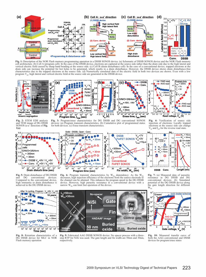
identical to that in our previous work [1] apart from a revamped nickel-silicide junction that uses a three-step RTP for precise control of the junction profile. In contrast, sacrificial oxidation, release, and gate trimming are newly added, and a gate spacer formation was omitted in the AAG DSSB SONOS device. SEM and TEM photographs of DG and AAG DSSB SONOS devices are shown at Fig.2 and Fig. 9, respectively. They ensure high immunity to short-channel and punchthrough in scaled NOR Flash memory.
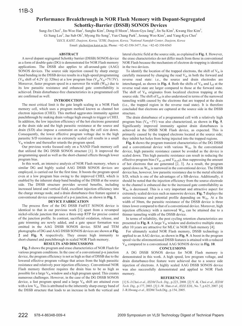
RESULTS AND DISCUSSIONS Fig. 3 shows the program and erase characteristics of NOR Flash for
various program conditions. In the case of a conventional p-n junction device, the program efficiency is not as high as that of DSSB due to the lowered effective program voltage that arises from the high parasitic resistance and relatively poor injection efficiency. Conventional NOR Flash memory therefore requires the drain bias to be as high as possible for a large Vth window and a high program speed. This creates numerous challenges. However, in the case of the DG DSSB SONOS device, a fast program speed and a large Vth shift are attained even with a low Vds. This is attributed to the inherently sharp energy band of the DSSB structure that leads to an increase in both the vertical and
lateral electric field at the source side, as explained in Fig. 1. However, the erase characteristics do not differ much from those in conventional NOR Flash because the mechanism of electron de-trapping is identical in the two devices.
To identify the location of the trapped electrons, the shift of Vth is carefully measured by changing the read Vds in both the forward and reverse read state: i.e., the source and drain electrodes are interchanged, as shown in Fig. 4. Both the shifts of Vth and Ioff at the reverse read state are larger compared to those at the forward state. The shift of Vth originates from localized electron trapping at the source side. The shift of Ioff is also understood in terms of the narrowed tunneling width caused by the electrons that are trapped at the drain (i.e., the trapped region in the reverse read state). It is therefore concluded that electrons are captured at the source side in the DSSB structure.
The drain disturbance of a programmed cell with a relatively high program bias (Vds =5V) was also characterized, as shown in Fig. 5.Significantly improved immunity against drain disturbances is achieved in the DSSB NOR Flash device, as expected. This is primarily caused by the trapped electrons located at the source side; they inhibit hot holes from being injected into the trapped regions.
Fig. 6 shows the program transient characteristics of the DG DSSB and a conventional device with various Wfin. In the conventional device, high parasitic resistance cannot be avoided as the device is scaled down. This high parasitic resistance can result in reducing the effective program bias (Vgs, eff and Vds,eff), thus suppressing the amount of hot electrons that are generated [2, 3]. As a result, the program speed slows as Wfin is narrowed in the conventional device. The DSSB device has, however, low parasitic resistance due to the metal silicided S/D, which is one of the advantages of a SB-device. Additionally, it should be noted that the injection efficiency from the source electrode to the channel is enhanced due to the increased gate controllability as Wfin is decreased. This is a very important and attractive aspect for extremely scaled devices such as nanowire devices. Fig. 7 displays the series resistance and potential profile depending on Wfin. At a fin width of 30nm, the parasitic resistance of the DSSB device is three times lower compared to that of a conventional device. Moreover, high injection efficiency with a narrowed Wfin can be attained due to a thinner tunneling width of the DSSB device.
In terms of reliability, the post cycling retention characteristics are presented in Fig. 8. A large Vth window and distinctive multiple states after 10 years are attractive for MLC in NOR Flash memory [4].
For ultimately scaled NOR Flash memory, DSSB technology is applied to an AAG device, as shown in Fig. 9. A boost in the program speed via the aforementioned DSSB features is attained with a reduced Vds compared to a conventional AAG SONOS device in Fig. 10.
CONCLUSIONSA DG DSSB SONOS device for NOR Flash memory is
demonstrated in this work. A high speed, low program voltage, and drain disturbance-free feature were achieved due to a source side injection of electrons. A highly scaled AAG DSSB SONOS device was also successfully demonstrated and applied to NOR Flash memory.
REFERENCES[1] S.-J.Choi et al., IEDM Tech. Dig., p.223, 2008. [2] Y.-K. Choi et al., IEDMTech. Dig., p.177, 2003. [3] J.-W. Han et al., IEEE EDL, No. 7, p.625, 2007. [4] J.-R.Hwang et al., IEDM Tech.Dig., p.154, 2005.
2232009 Symposium on VLSI Technology Digest of Technical Papers
Fig. 8: Retention characteristics of a DG DSSB device for MLC in NOR Flash memory operation
50 nm Buriedoxide
NiSi
Fin
GateNo-spacer a-a’
HADAAF image
200nm
Lg
Lg=50nmWfin=30nm
b
b’a
a’
50 nm Buried oxide
Control gateO/N/O = 3/6/11nm
NiSi
Fin
b-b’
100 101 102 103 104 105 106 107 108 109-1
0
1
2
3
4
5
6
7
tPGM = 32ns
tPGM = 320ns
tPGM = 1ms
Erased, VERS=-15V, tERS=10ms
Lg = 300nmWfin = 30nm
After 1k cycling, Program : Vgs=8V, Vds=4V
10 years
Thre
shol
d vo
ltage
, Vth (V
)
Time (sec)0 1 2 3 4 5 6
10-12
10-11
10-10
10-9
10-8
10-7
10-6
10-5
Lg=50nmWfin=30nm
VERS=-12VtERS=1 s
AAG Conv.SONOS
AAG DSSB SONOS
Vgs
/Vds
=10V/3.5VtPGM=10 s
Erased
Programmed
Drai
n cu
rren
t, I ds
(A)
Gate voltage, Vgs (V)50 nm Buriedoxide
NiSi
Fin
GateNo-spacer a-a’
HADAAF image
50 nm Buriedoxide
NiSi
Fin
GateNo-spacer a-a’
HADAAF image
200nm
Lg
Lg=50nmWfin=30nm
b
b’a
a’
50 nm Buried oxide
Control gateO/N/O = 3/6/11nm
NiSi
Fin
b-b’
50 nm Buried oxide
Control gateO/N/O = 3/6/11nm
NiSi
Fin
b-b’
100 101 102 103 104 105 106 107 108 109-1
0
1
2
3
4
5
6
7
tPGM = 32ns
tPGM = 320ns
tPGM = 1ms
Erased, VERS=-15V, tERS=10ms
Lg = 300nmWfin = 30nm
After 1k cycling, Program : Vgs=8V, Vds=4V
10 years
Thre
shol
d vo
ltage
, Vth (V
)
Time (sec)0 1 2 3 4 5 6
10-12
10-11
10-10
10-9
10-8
10-7
10-6
10-5
Lg=50nmWfin=30nm
VERS=-12VtERS=1 s
AAG Conv.SONOS
AAG DSSB SONOS
Vgs
/Vds
=10V/3.5VtPGM=10 s
Erased
Programmed
Drai
n cu
rren
t, I ds
(A)
Gate voltage, Vgs (V)
0.0
0.5
1.0
1.5
2.0
2.5
3.0
Wfin = 30nm Wfin = 50nm Wfin = 70nm
NiSi
@ Voverdrive=1VVds = 0.05 V
Conv.DSSB
R para
sitic
(km
)
-1 0 1 2 3 40.0
0.1
0.2
0.3
0.4
0.5
0.6
0.7
Barr
ier h
eigh
t
@ On-state V
gs = 2V
Vds
= 1V
Wfin = 70nm Wfin = 30nm
Pote
ntia
l (V)
Length (nm)
(a) (b)
10-8 10-7 10-6 10-5 10-4 10-3 10-2 10-1
1.0
1.5
2.0
2.5
3.0
3.5
4.0
4.5
5.0
O/N/O=3/6/4nmLg = 300nmwfin = 30nm
Programmedcells
Thre
shol
d vo
ltage
, Vth (V
)
Drain disturb time (sec)
DSSB Vgs=0V / Vds=5V Conv. Vgs=0V / Vds=5V
30 40 50 60 700
1
2
3
4
5
6
Lg=300nmWfin=30nm
DSSBFinFET SONOS
ConventionalFinFET SONOS
Vgs=7VVds=3VtPGM=10 s
Thre
shol
d vo
ltage
, Vth (V
)
Fin width, Wfin (nm)10-8 10-7 10-6 10-5 10-4 10-3 10-2
0
1
2
3
4
5
6
Wfin = 70nm
Wfin = 70nm
Wfin = 30nm
Wfin = 30nm
Lg = 300nm
Solid : DSSB, Open : ConvProgram conditionVgs = 7VVds = 3V
Thre
shol
d vo
ltage
, Vth (V
)
Program time (sec)
10-8 10-7 10-6 10-5 10-4 10-3 10-2 10-1
0
1
2
3
4
5
6
7
O/N/O=3/6/4nmConventionalSONOS
DSSBSONOS
Lg = 300nmWfin = 30nm
Vg / Vd
8V/4V7V/4V7V/3V
Thre
shol
d vo
ltage
, Vth (V
)
Program time, tPGM (sec)
(a)
-1 0 1 2 3 4 5 6
0.0
0.2
0.4
0.6
0.8
1.0
DSSBConv.
Vgs
=7VVds=3V
tPGM=1 s
Cum
ulat
ive
(%)
Vth (V)
(b)
10-8 10-7 10-6 10-5 10-4 10-3 10-2 10-1 1000
1
2
3
4
5
O/N/O=3/6/4nmVERS=-15V, -14V
Lg = 300nmWfin = 30nmTh
resh
old
volta
ge, V
th (V
)Erase time, tERS (sec)
DSSB Conv.
(c)
0.0 0.5 1.0 1.5 2.0-2.0
-1.5
-1.0
-0.5
0.0
Vth =Vth(Vds=0.05)-Vth(read Vds)
Lg = 300nmWfin = 30nm
FWD read RVD read
FWD read RVD read
V th s
hift,
V th
(V)
Read voltage, Vds (V)0.0 0.5 1.0 1.5 2.0
10-13
10-12
10-11
10-10
10-9
10-8
10-7
Ioff@ Vg=Vth-1
Vg = 7VVd = 3V
Program timetPGM = 320ns
Off
curr
ent,
I off (
A)
Buried oxide50 nm
Controlgate
Hardmask
Sichannel
O/N/O
0 10 20 30 40
Inte
nsity
(a.u
.)
Depth (nm)
Si
As
NiSi/Siinterface
EDSdirection
NiSi
Arsenic segregation 10-8 10-7 10-6 10-5 10-4 10-3 10-2 10-1
0
1
2
3
4
5
6
7
O/N/O=3/6/4nmConventionalSONOS
DSSBSONOS
Lg = 300nmWfin = 30nm
Vg / Vd
8V/4V7V/4V7V/3V
Thre
shol
d vo
ltage
, Vth (V
)
Program time, tPGM (sec)
(a)
10-8 10-7 10-6 10-5 10-4 10-3 10-2 10-1
0
1
2
3
4
5
6
7
O/N/O=3/6/4nmConventionalSONOS
DSSBSONOS
Lg = 300nmWfin = 30nm
Vg / Vd
8V/4V7V/4V7V/3V
Thre
shol
d vo
ltage
, Vth (V
)
Program time, tPGM (sec)
(a)
-1 0 1 2 3 4 5 6
0.0
0.2
0.4
0.6
0.8
1.0
DSSBConv.
Vgs=7VVds=3V
tPGM=1 s
Cum
ulat
ive
(%)
Vth (V)
(b)
-1 0 1 2 3 4 5 6
0.0
0.2
0.4
0.6
0.8
1.0
DSSBConv.
Vgs=7VVds=3V
tPGM=1 s
Cum
ulat
ive
(%)
Vth (V)
(b)
10-8 10-7 10-6 10-5 10-4 10-3 10-2 10-1 1000
1
2
3
4
5
O/N/O=3/6/4nmVERS=-15V, -14V
Lg = 300nmWfin = 30nmTh
resh
old
volta
ge, V
th (V
)Erase time, tERS (sec)
DSSB Conv.
(c)
10-8 10-7 10-6 10-5 10-4 10-3 10-2 10-1 1000
1
2
3
4
5
O/N/O=3/6/4nmVERS=-15V, -14V
Lg = 300nmWfin = 30nmTh
resh
old
volta
ge, V
th (V
)Erase time, tERS (sec)
DSSB Conv.
(c)
0.0 0.5 1.0 1.5 2.0-2.0
-1.5
-1.0
-0.5
0.0
Vth =Vth(Vds=0.05)-Vth(read Vds)
Lg = 300nmWfin = 30nm
FWD read RVD read
FWD read RVD read
V th s
hift,
V th
(V)
Read voltage, Vds (V)0.0 0.5 1.0 1.5 2.0
10-13
10-12
10-11
10-10
10-9
10-8
10-7
Ioff@ Vg=Vth-1
Vg = 7VVd = 3V
Program timetPGM = 320ns
Off
curr
ent,
I off (
A)
Buried oxide50 nm
Controlgate
Hardmask
Sichannel
O/N/O
0 10 20 30 40
Inte
nsity
(a.u
.)
Depth (nm)
Si
As
NiSi/Siinterface
EDSdirection
NiSi
Arsenic segregation
Fig. 1: Description of the NOR Flash memory programming operation in a DSSB SONOS device. (a) Schematic of DSSB SONOS device and the NOR Flash memory cell architecture. (b) Cell A (program cell): In the case of the DSSB device, electrons are captured at the source side rather than the drain side due to the high lateral and vertical electric field caused by sharp band bending at the source side. (c) Cell B (drain disturbance cell): In the case of a conventional device, trapped electrons at the drain side can increase the potential for hot holes to be generated, which results in a drain disturbance. However, the DSSB device shows drain disturbance-free characteristics due to the trapped electrons at the source side. (d) Numerically simulated data of the electric field in both two devices are shown. Even with a low program Vds, high lateral and vertical electric field at the source side are generated in the DSSB device.
Fig. 2: STEM EDS analysis and TEM image of DG DSSB SONOS (a-a’ direction of Fig. 1(a)
Fig. 3: Program/erase characteristics for DG DSSB and DG conventional SONOS devices: (a) Program transient characteristics. (b) Cumulative plot of programmed states for both devices. (c) Erase transient characteristics.
Fig. 4: Verification of source side injection of electrons: Locally trapped electrons at the source side can change Vth and Ioff for the reverse read state.
Fig. 5: Drain disturbance of DG DSSB and DG conventional devices: Compared to the conventional device, high immunity to drain disturbance is achieved in the DG DSSB device.
Fig. 6: Program transient characteristics by Wfin dependency: As the Wfindecreases, high injection efficiency of the electrons from the source electrode to the channel can be attained. This enhances the program speed in the DG DSSB device. However, high parasitic resistance in a conventional device with a narrow Wfin can limit fast operation of the device.
Fig. 7: (a) Measured data of parasitic resistance in DG DSSB and DG conventional devices: (b) Simulated potential of the DG DSSB device along the gate length direction for different Wfin
Fig. 9: Fabricated AAG DSSB SONOS device: No spacer process with a three-step RTP for NiSi was used. The gate length and fin width are 50nm and 30nm, respectively.
Fig. 10: Measured transfer curve of both the AAG conventional and DSSB devices for program/erase states
(c)(b) (d)
n+
NiSi
NiSi
(1)
(2)
Silicon
Silicon
Vds
Vds
n+
High vertical fieldHigh lateral field
Low vertical fieldHigh lateral field
DSSB device
Conv. device
NiSi
NiSi
n+
n+
Low draindisturbance
High draindisturbance
Silicon
Silicon
(1)
(2)
DSSB device
Conv. device
Cell A : a-a’ direction Cell B : a-a’ direction(a)
Controlgate
Source Drain
Controlgate
a a’(1) (2)
PGM BL(Vds=4V)
Programmingcell (Vgs=7V)
Programmeddrain disturbancecell (Vgs=0V)
Cell A
Cell B
CSL
<Programming & disturbance cell> 0.0
0.2
0.4
0.6
0.8
1.0
1.2
1.4
1.6
1.8
2.0
Vertical fieldConv. : Vgd=Vg-VdDSSB : V
gs=V
g-V
s
Vds=3, 4VSource
Vds=3, 4VDrain
Vgs=7V
DSSBConv.
Late
ral e
.fiel
d (M
V/cm
)
Control gate
Substrate
Buried oxide
NiSi (S/D)a
a’
O/N/O