11/2008 PCI – PCI-X Analyzer &...
18
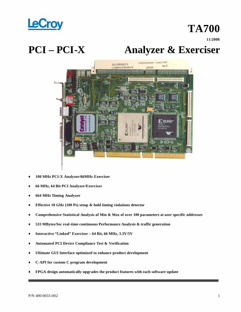
TA700 P/N 400-0033-002 1 11/2008 PCI – PCI-X Analyzer & Exerciser ♦ 100 MHz PCI-X Analyzer/66MHz Exerciser ♦ 66 MHz, 64 Bit PCI Analyzer/Exerciser ♦ 664 MHz Timing Analyzer ♦ Effective 10 GHz (100 Ps) setup & hold timing violations detector ♦ Comprehensive Statistical Analysis of Min & Max of over 100 parameters at user specific addresses ♦ 533 MBytes/Sec real-time continuous Performance Analysis & traffic generation ♦ Interactive “Linked” Exerciser – 64 Bit, 66 MHz, 3.3V/5V ♦ Automated PCI Device Compliance Test & Verification ♦ Ultimate GUI Interface optimized to enhance product development ♦ C-API for custom C program development ♦ FPGA design automatically upgrades the product features with each software update
Transcript of 11/2008 PCI – PCI-X Analyzer &...
TA700
P/N 400-0033-002 1
11/2008
PCI – PCI-X Analyzer & Exerciser
♦ 100 MHz PCI-X Analyzer/66MHz Exerciser
♦ 66 MHz, 64 Bit PCI Analyzer/Exerciser
♦ 664 MHz Timing Analyzer
♦ Effective 10 GHz (100 Ps) setup & hold timing violations detector
♦ Comprehensive Statistical Analysis of Min & Max of over 100 parameters at user specific addresses
♦ 533 MBytes/Sec real-time continuous Performance Analysis & traffic generation
♦ Interactive “Linked” Exerciser – 64 Bit, 66 MHz, 3.3V/5V
♦ Automated PCI Device Compliance Test & Verification
♦ Ultimate GUI Interface optimized to enhance product development
♦ C-API for custom C program development
♦ FPGA design automatically upgrades the product features with each software update
TA700
2
PCI BUS, TARGET SYSTEM
Analyze any PCI or PCI-X System Architecture running under any operating system.
HOST SOFTWARE
The TA700 software operates under Windows XP, 2000, NT SP 3.1 or higher, 98 or 95.
FIELD UPGRADABLE FPGA based design allows automatic hardware upgrade to the latest added features each time a new version of the software is loaded.
AUXILIARY PCI CONNECTOR
An auxiliary connector on top of the TA700 PCI analyzer card provides an expansion slot for our PCI device.
The TA700 has an on board arbiter that handles the REQ# and GNT# betwee0n the TA700 and the DUT on top, allowing both cards to act as Master.
Hot swap utility software allows automatic reconfiguration of UUT registers without rebooting.
The expansion slot is useful for systems with limited available PCI slots.
AUTOMATIC SYSTEM CLOCK DETECTION
The TA700 automatically detects and reports the system clock frequency.
VOLTAGE CHECK You may enable the TA700 to monitor the system voltages and the +5V DUT voltage for a drop exceeding 5% of nominal and to flag this by illuminating a red LED.
It is not recommended to operate the TA700 with the extender at frequencies above 66 MHz.
TA700
3
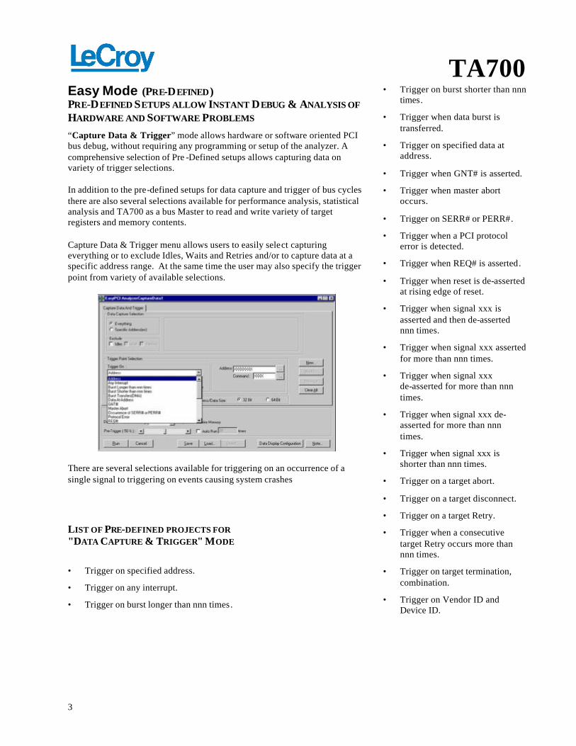
Easy Mode (PRE-DEFINED) PRE-DEFINED SETUPS ALLOW INSTANT DEBUG & ANALYSIS OF HARDWARE AND SOFTWARE PROBLEMS
“Capture Data & Trigger” mode allows hardware or software oriented PCI bus debug, without requiring any programming or setup of the analyzer. A comprehensive selection of Pre -Defined setups allows capturing data on variety of trigger selections.
In addition to the pre-defined setups for data capture and trigger of bus cycles there are also several selections available for performance analysis, statistical analysis and TA700 as a bus Master to read and write variety of target registers and memory contents.
Capture Data & Trigger menu allows users to easily select capturing everything or to exclude Idles, Waits and Retries and/or to capture data at a specific address range. At the same time the user may also specify the trigger point from variety of available selections.
There are several selections available for triggering on an occurrence of a single signal to triggering on events causing system crashes
LIST OF PRE-DEFINED PROJECTS FOR "DATA CAPTURE & TRIGGER" MODE
• Trigger on specified address.
• Trigger on any interrupt.
• Trigger on burst longer than nnn times.
• Trigger on burst shorter than nnn times.
• Trigger when data burst is transferred.
• Trigger on specified data at address.
• Trigger when GNT# is asserted.
• Trigger when master abort occurs.
• Trigger on SERR# or PERR#.
• Trigger when a PCI protocol error is detected.
• Trigger when REQ# is asserted.
• Trigger when reset is de-asserted at rising edge of reset.
• Trigger when signal xxx is asserted and then de-asserted nnn times.
• Trigger when signal xxx asserted for more than nnn times.
• Trigger when signal xxx de-asserted for more than nnn times.
• Trigger when signal xxx de-asserted for more than nnn times.
• Trigger when signal xxx is shorter than nnn times.
• Trigger on a target abort.
• Trigger on a target disconnect.
• Trigger on a target Retry.
• Trigger when a consecutive target Retry occurs more than nnn times.
• Trigger on target termination, combination.
• Trigger on Vendor ID and Device ID.
TA700
4
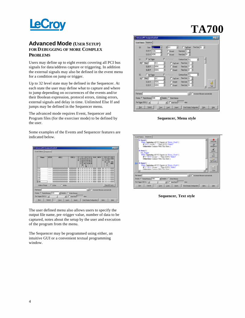
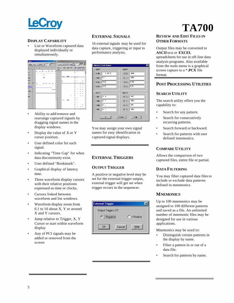
Advanced Mode (USER SETUP) FOR DEBUGGING OF MORE COMPLEX PROBLEMS Users may define up to eight events covering all PCI bus signals for data/address capture or triggering. In addition the external signals may also be defined in the event menu for a condition on jump or trigger.
Up to 32 level state may be defined in the Sequencer. At each state the user may define what to capture and where to jump depending on occurrences of the events and/or their Boolean expression, protocol errors, timing errors, external signals and delay in time. Unlimited Else If and jumps may be defined in the Sequencer menu.
The advanced mode requires Event, Sequencer and Program files (for the exerciser mode) to be defined by the user.
Some examples of the Events and Sequencer features are indicated below.
The user defined menu also allows users to specify the output file name, pre -trigger value, number of data to be captured, notes about the setup by the user and execution of the program from the menu.
The Sequencer may be programmed using either, an intuitive GUI or a convenient textual programming window.
Sequencer, Menu style
Sequencer, Text style
TA700
5
DISPLAY CAPABILITY • List or Waveform captured data
displayed individually or simultaneously.
• Ability to add/remove and rearrange captured signals by dragging signal names in the display windows.
• Display the value of X or Y cursor position.
• User defined color for each signal.
• Indicating "Time Gap" for when data discontinuity exist.
• User defined "Bookmark".
• Graphical display of latency time.
• Three waveform display cursors with their relative positions expressed as time or clocks.
• Cursors linked between waveform and list windows.
• Waveform display zoom from 0.1 to 10 about X, Y or around X and Y cursors.
• Jump relative to Trigger, X, Y Cursor or start within waveform display
• Any of PCI signals may be added or removed from the screen
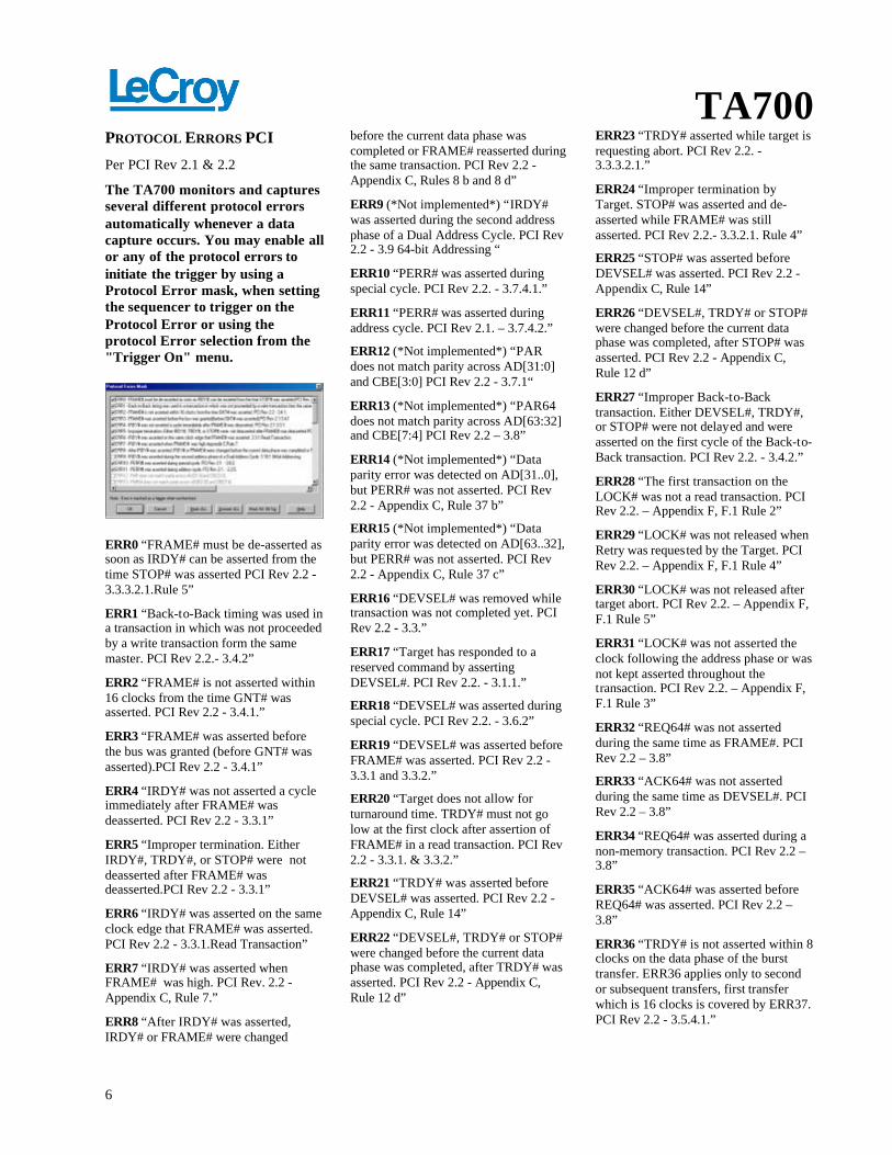
EXTERNAL SIGNALS 16 external signals may be used for data capture, triggering or input to performance analysis.
You may assign your own signal names for easy identification in captured signal displays.
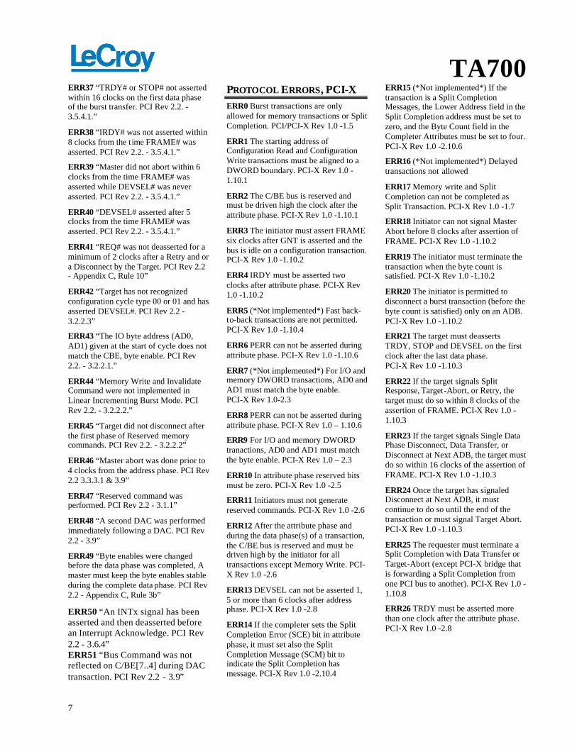
EXTERNAL TRIGGERS
OUTPUT TRIGGER
A positive or negative level may be set for the external trigger output, external trigger will get set when trigger occurs in the sequencer.
REVIEW AND EDIT FILES IN OTHER FORMATS
Output files may be converted to ASCII text or EXCEL spreadsheets for use in off-line data analysis programs. Also available from the tools menu is a graphical screen capture to a * .PCX file format.
POST PROCESSING UTILITIES
SEARCH UTILITY
The search utility offers you the capability to:
• Search for any pattern.
• Search for consecutively recurring patterns.
• Search forward or backward.
• Search for patterns with user defined mnemonics.
COMPARE UTILITY
Allows the comparison of two captured files, entire file or partial.
DATA FILTERING
You may filter captured data files to include or exclude data patterns defined in mnemonics.
MNEMONICS Up to 100 mnemonics may be assigned to 100 different patterns and saved as a file. An unlimited number of mnemonic files may be designed for use in various applications.
Mnemonics may be used to: • Distinguish certain patterns in
the display by name.
• Filter a pattern in or out of a data file.
• Search for patterns by name.
TA700
6
PROTOCOL ERRORS PCI
Per PCI Rev 2.1 & 2.2
The TA700 monitors and captures several different protocol errors automatically whenever a data capture occurs. You may enable all or any of the protocol errors to initiate the trigger by using a Protocol Error mask, when setting the sequencer to trigger on the Protocol Error or using the protocol Error selection from the "Trigger On" menu.
ERR0 “FRAME# must be de-asserted as soon as IRDY# can be asserted from the time STOP# was asserted PCI Rev 2.2 -3.3.3.2.1.Rule 5”
ERR1 “Back-to-Back timing was used in a transaction in which was not proceeded by a write transaction form the same master. PCI Rev 2.2.- 3.4.2”
ERR2 “FRAME# is not asserted within 16 clocks from the time GNT# was asserted. PCI Rev 2.2 - 3.4.1.”
ERR3 “FRAME# was asserted before the bus was granted (before GNT# was asserted).PCI Rev 2.2 - 3.4.1”
ERR4 “IRDY# was not asserted a cycle immediately after FRAME# was deasserted. PCI Rev 2.2 - 3.3.1”
ERR5 “Improper termination. Either IRDY#, TRDY#, or STOP# were not deasserted after FRAME# was deasserted.PCI Rev 2.2 - 3.3.1”
ERR6 “IRDY# was asserted on the same clock edge that FRAME# was asserted. PCI Rev 2.2 - 3.3.1.Read Transaction”
ERR7 “IRDY# was asserted when FRAME# was high. PCI Rev. 2.2 - Appendix C, Rule 7.”
ERR8 “After IRDY# was asserted, IRDY# or FRAME# were changed
before the current data phase was completed or FRAME# reasserted during the same transaction. PCI Rev 2.2 -Appendix C, Rules 8 b and 8 d”
ERR9 (*Not implemented*) “IRDY# was asserted during the second address phase of a Dual Address Cycle. PCI Rev 2.2 - 3.9 64-bit Addressing “
ERR10 “PERR# was asserted during special cycle. PCI Rev 2.2. - 3.7.4.1.”
ERR11 “PERR# was asserted during address cycle. PCI Rev 2.1. – 3.7.4.2.”
ERR12 (*Not implemented*) “PAR does not match parity across AD[31:0] and CBE[3:0] PCI Rev 2.2 - 3.7.1“
ERR13 (*Not implemented*) “PAR64 does not match parity across AD[63:32] and CBE[7:4] PCI Rev 2.2 – 3.8”
ERR14 (*Not implemented*) “Data parity error was detected on AD[31..0], but PERR# was not asserted. PCI Rev 2.2 - Appendix C, Rule 37 b”
ERR15 (*Not implemented*) “Data parity error was detected on AD[63..32], but PERR# was not asserted. PCI Rev 2.2 - Appendix C, Rule 37 c”
ERR16 “DEVSEL# was removed while transaction was not completed yet. PCI Rev 2.2 - 3.3.”
ERR17 “Target has responded to a reserved command by asserting DEVSEL#. PCI Rev 2.2. - 3.1.1.”
ERR18 “DEVSEL# was asserted during special cycle. PCI Rev 2.2. - 3.6.2”
ERR19 “DEVSEL# was asserted before FRAME# was asserted. PCI Rev 2.2 - 3.3.1 and 3.3.2.”
ERR20 “Target does not allow for turnaround time. TRDY# must not go low at the first clock after assertion of FRAME# in a read transaction. PCI Rev 2.2 - 3.3.1. & 3.3.2.”
ERR21 “TRDY# was asserted before DEVSEL# was asserted. PCI Rev 2.2 - Appendix C, Rule 14”
ERR22 “DEVSEL#, TRDY# or STOP# were changed before the current data phase was completed, after TRDY# was asserted. PCI Rev 2.2 - Appendix C, Rule 12 d”
ERR23 “TRDY# asserted while target is requesting abort. PCI Rev 2.2. - 3.3.3.2.1.”
ERR24 “Improper termination by Target. STOP# was asserted and de-asserted while FRAME# was still asserted. PCI Rev 2.2.- 3.3.2.1. Rule 4”
ERR25 “STOP# was asserted before DEVSEL# was asserted. PCI Rev 2.2 -Appendix C, Rule 14”
ERR26 “DEVSEL#, TRDY# or STOP# were changed before the current data phase was completed, after STOP# was asserted. PCI Rev 2.2 - Appendix C, Rule 12 d”
ERR27 “Improper Back-to-Back transaction. Either DEVSEL#, TRDY#, or STOP# were not delayed and were asserted on the first cycle of the Back-to-Back transaction. PCI Rev 2.2. - 3.4.2.”
ERR28 “The first transaction on the LOCK# was not a read transaction. PCI Rev 2.2. – Appendix F, F.1 Rule 2”
ERR29 “LOCK# was not released when Retry was requested by the Target. PCI Rev 2.2. – Appendix F, F.1 Rule 4”
ERR30 “LOCK# was not released after target abort. PCI Rev 2.2. – Appendix F, F.1 Rule 5”
ERR31 “LOCK# was not asserted the clock following the address phase or was not kept asserted throughout the transaction. PCI Rev 2.2. – Appendix F, F.1 Rule 3”
ERR32 “REQ64# was not asserted during the same time as FRAME#. PCI Rev 2.2 – 3.8”
ERR33 “ACK64# was not asserted during the same time as DEVSEL#. PCI Rev 2.2 – 3.8”
ERR34 “REQ64# was asserted during a non-memory transaction. PCI Rev 2.2 – 3.8”
ERR35 “ACK64# was asserted before REQ64# was asserted. PCI Rev 2.2 – 3.8”
ERR36 “TRDY# is not asserted within 8 clocks on the data phase of the burst transfer. ERR36 applies only to second or subsequent transfers, first transfer which is 16 clocks is covered by ERR37. PCI Rev 2.2 - 3.5.4.1.”
TA700
7
ERR37 “TRDY# or STOP# not asserted within 16 clocks on the first data phase of the burst transfer. PCI Rev 2.2. - 3.5.4.1.”
ERR38 “IRDY# was not asserted within 8 clocks from the time FRAME# was asserted. PCI Rev 2.2. - 3.5.4.1.”
ERR39 “Master did not abort within 6 clocks from the time FRAME# was asserted while DEVSEL# was never asserted. PCI Rev 2.2. - 3.5.4.1.”
ERR40 “DEVSEL# asserted after 5 clocks from the time FRAME# was asserted. PCI Rev 2.2. - 3.5.4.1.”
ERR41 “REQ# was not deasserted for a minimum of 2 clocks after a Retry and or a Disconnect by the Target. PCI Rev 2.2 - Appendix C, Rule 10”
ERR42 “Target has not recognized configuration cycle type 00 or 01 and has asserted DEVSEL#. PCI Rev 2.2 - 3.2.2.3”
ERR43 “The IO byte address (AD0, AD1) given at the start of cycle does not match the CBE, byte enable. PCI Rev 2.2. - 3.2.2.1.”
ERR44 “Memory Write and Invalidate Command were not implemented in Linear Incrementing Burst Mode. PCI Rev 2.2. - 3.2.2.2.”
ERR45 “Target did not disconnect after the first phase of Reserved memory commands. PCI Rev 2.2. - 3.2.2.2”
ERR46 “Master abort was done prior to 4 clocks from the address phase. PCI Rev 2.2 3.3.3.1 & 3.9”
ERR47 “Reserved command was performed. PCI Rev 2.2 - 3.1.1”
ERR48 “A second DAC was performed immediately following a DAC. PCI Rev 2.2 - 3.9”
ERR49 “Byte enables were changed before the data phase was completed, A master must keep the byte enables stable during the complete data phase. PCI Rev 2.2 - Appendix C, Rule 3b”
ERR50 “An INTx signal has been asserted and then deasserted before an Interrupt Acknowledge. PCI Rev 2.2 - 3.6.4” ERR51 “Bus Command was not reflected on C/BE[7..4] during DAC transaction. PCI Rev 2.2 - 3.9”
PROTOCOL ERRORS, PCI-X ERR0 Burst transactions are only allowed for memory transactions or Split Completion. PCI/PCI-X Rev 1.0 -1.5
ERR1 The starting address of Configuration Read and Configuration Write transactions must be aligned to a DWORD boundary. PCI-X Rev 1.0 -1.10.1
ERR2 The C/BE bus is reserved and must be driven high the clock after the attribute phase. PCI-X Rev 1.0 -1.10.1
ERR3 The initiator must assert FRAME six clocks after GNT is asserted and the bus is idle on a configuration transaction. PCI-X Rev 1.0 -1.10.2
ERR4 IRDY must be asserted two clocks after attribute phase. PCI-X Rev 1.0 -1.10.2
ERR5 (*Not implemented*) Fast back-to-back transactions are not permitted. PCI-X Rev 1.0 -1.10.4
ERR6 PERR can not be asserted during attribute phase. PCI-X Rev 1.0 -1.10.6
ERR7 (*Not implemented*) For I/O and memory DWORD transactions, AD0 and AD1 must match the byte enable. PCI-X Rev 1.0-2.3
ERR8 PERR can not be asserted during attribute phase. PCI-X Rev 1.0 – 1.10.6
ERR9 For I/O and memory DWORD tranactions, AD0 and AD1 must match the byte enable. PCI-X Rev 1.0 – 2.3
ERR10 In attribute phase reserved bits must be zero. PCI-X Rev 1.0 -2.5
ERR11 Initiators must not generate reserved commands. PCI-X Rev 1.0 -2.6
ERR12 After the attribute phase and during the data phase(s) of a transaction, the C/BE bus is reserved and must be driven high by the initiator for all transactions except Memory Write. PCI-X Rev 1.0 -2.6
ERR13 DEVSEL can not be asserted 1, 5 or more than 6 clocks after address phase. PCI-X Rev 1.0 -2.8
ERR14 If the completer sets the Split Completion Error (SCE) bit in attribute phase, it must set also the Split Completion Message (SCM) bit to indicate the Split Completion has message. PCI-X Rev 1.0 -2.10.4
ERR15 (*Not implemented*) If the transaction is a Split Completion Messages, the Lower Address field in the Split Completion address must be set to zero, and the Byte Count field in the Completer Attributes must be set to four. PCI-X Rev 1.0 -2.10.6
ERR16 (*Not implemented*) Delayed transactions not allowed
ERR17 Memory write and Split Completion can not be completed as Split Transaction. PCI-X Rev 1.0 -1.7
ERR18 Initiator can not signal Master Abort before 8 clocks after assertion of FRAME. PCI-X Rev 1.0 -1.10.2
ERR19 The initiator must terminate the transaction when the byte count is satisfied. PCI-X Rev 1.0 -1.10.2
ERR20 The initiator is permitted to disconnect a burst transaction (before the byte count is satisfied) only on an ADB. PCI-X Rev 1.0 -1.10.2
ERR21 The target must deasserts TRDY, STOP and DEVSEL on the first clock after the last data phase. PCI-X Rev 1.0 -1.10.3
ERR22 If the target signals Split Response, Target-Abort, or Retry, the target must do so within 8 clocks of the assertion of FRAME. PCI-X Rev 1.0 -1.10.3
ERR23 If the target signals Single Data Phase Disconnect, Data Transfer, or Disconnect at Next ADB, the target must do so within 16 clocks of the assertion of FRAME. PCI-X Rev 1.0 -1.10.3
ERR24 Once the target has signaled Disconnect at Next ADB, it must continue to do so until the end of the transaction or must signal Target Abort. PCI-X Rev 1.0 -1.10.3
ERR25 The requester must terminate a Split Completion with Data Transfer or Target-Abort (except PCI-X bridge that is forwarding a Split Completion from one PCI bus to another). PCI-X Rev 1.0 -1.10.8
ERR26 TRDY must be asserted more than one clock after the attribute phase. PCI-X Rev 1.0 -2.8
TA700
8
ERR27 If a transaction has four or more data phases, the initiator signals the end of the transaction by deasserting FRAME one clock before the last data phase. PCI-X Rev 1.0 -2.11.1.1
ERR28 The initiator must deassert FRAME at least two clocks after the target asserts TRDY. PCI-X Rev 1.0 -2.11.1.1
ERR29 The initiator must deassert IRDY one clock after the last data phase but never less than two clocks after the first data phase. PCI-X Rev 1.0 -2.11.1.1
ERR30 Not a valid termination with respect to IRDY, FRAME. PCI-X Rev 1.0 – 2.11.1.1
ERR31 (*Not implemented*) If the target signals Disconnect at Next ADB less than four data phases from an ADB the transaction must cross that ADB and disconnects on the next one. PCI-X Rev 1.0 -2.11.2.2
ERR32 Single Data Phase Disconnect, Retry or Split Response must be signaled in the first data phase. PCI-X Rev 1.0 -2.11.2
ERR33 Master can not insert wait states. PCI-X Rev 1.0 -1.6
ERR34 Target can not insert wait states after first data phase. PCI-X Rev 1.0 -1.6
ERR35 Target initial wait states for memory write and Split Completion transactions must come in pairs. PCI-X Rev 1.0 -1.6
ERR36 REQ64 can be asserted only for memory transactions (except Memory Read DWORD) or Split Completion. PCI-X Rev 1.0 -1.10.1
ERR37 (*Not implemented*) Dual transactions should not be used for addresses less that 4GB
ERR38 (*Not implemented*) Dual address & split.
ERR39 The first transaction on the LOCK# was not a read transaction. PCI-X Rev 1.0 - 8.5.1
ERR40 LOCK# was not released when Retry was requested by the Target. PCI-X Rev 1.0 - 8.5.1
ERR41 LOCK# was not released after target abort. PCI-X Rev 1.0 - 8.5.1
ERR42 LOCK# was not asserted the clock following the address phase or was not kept asserted throughout the transaction. PCI-X Rev 1.0 - 8.5.1
ERR43 Target has not recognized configuration cycle type 00 or 01 and has asserted DEVSEL#. PCI-X Rev 1.0 - 1.10.5
ERR44 Target has responded to a reserved command by asserting DEVSEL#. PCI-X Rev 1.0 - 2.4
ERR45 DEVSEL# was asserted during special cycle. PCI-X Rev 1.0 - 2.7.3
ERR46 FRAME# was asserted before the bus was granted (before GNT# was asserted). PCI-X Rev 1.0 - 1.10.2
ERR47 (*Overlapped Error*) IRDY# was asserted during the second address phase of a Dual Address Cycle. PCI-X Rev 1.0 - 2.12.1
ERR48 Reserved command was performed. PCI-X Rev 1.0 - 2.4
ERR49 PERR# was asserted during special cycle. PCI-X Rev 1.0 - 1.10.6
ERR50 PERR# was asserted during address cycle. PCI-X Rev 1.0 - 5
ERR51 PAR does not match parity across AD[31:0] and CBE[3:0]
ERR52 PAR64 does not match parity across AD[63:32] and CBE[7:4].
ERR53 Data parity error was detected on AD[31..0], but PERR# was not asserted. PCI-X Rev 1.0 - 1.10.6
ERR54 Data parity error was detected on AD[63..32], but PERR# was not asserted. PCI-X Rev 1.0 - 1.10.6
ERR55 REQ64# was not asserted during the same time as FRAME#. PCI-X Rev 1.0 - 2.12.3
ERR56 ACK64# was not asserted during the same time as DEVSEL#. PCI-X Rev 1.0 – 1.12.3
ERR57 ACK64# was asserted before REQ64# was asserted. PCI-X Rev 1.0 – 2.12.3
ERR58 Bus Command was not reflected on C/BE[7..4] during DAC transaction. PCI-X Rev 1.0 – 2.12.1
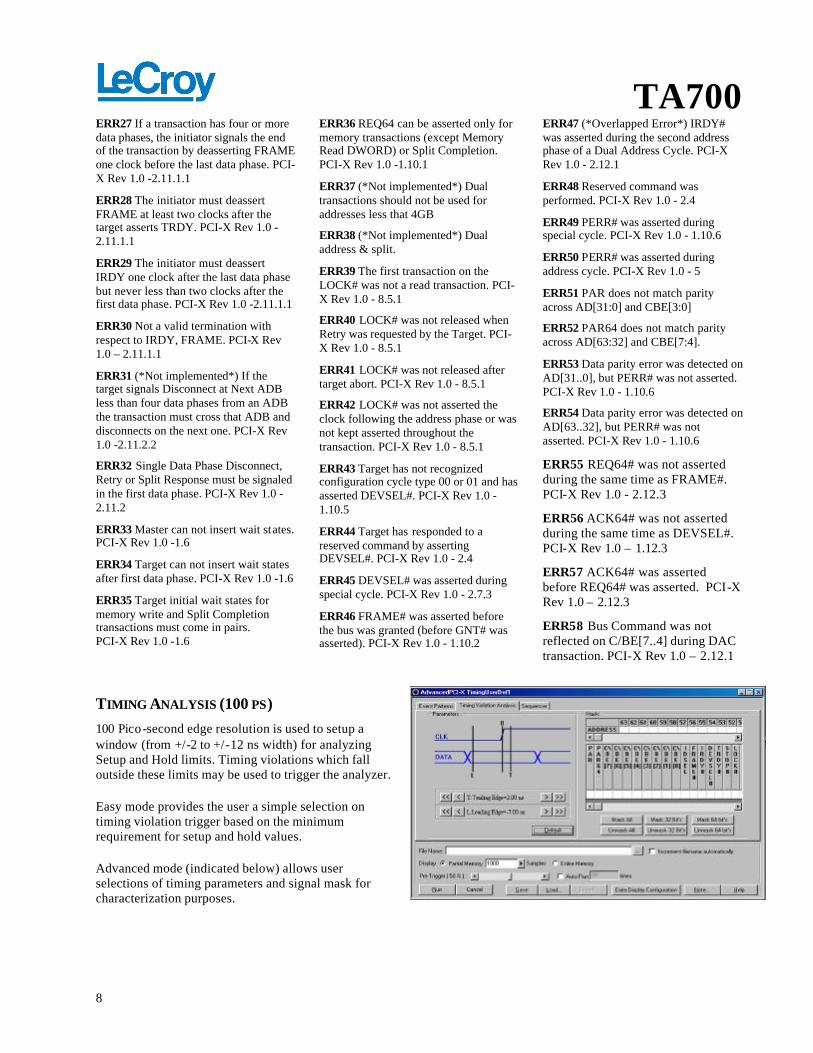
TIMING ANALYSIS (100 PS) 100 Pico-second edge resolution is used to setup a window (from +/-2 to +/-12 ns width) for analyzing Setup and Hold limits. Timing violations which fall outside these limits may be used to trigger the analyzer.
Easy mode provides the user a simple selection on timing violation trigger based on the minimum requirement for setup and hold values.
Advanced mode (indicated below) allows user selections of timing parameters and signal mask for characterization purposes.
TA700
9
• Any PCI signal may be included or excluded for monitoring timing violation.
• Any bus “glitch” greater than 1.5 ns is captured as a timing violation.
• All timing violations are captured in memory and may be displayed in sync with the bus signals.
TIMING ANALYSIS 664 MHZ An optional timing analysis of 664 MHz is available to sample data with a time reference asynchronous to the bus clock. This feature is useful in sampling the bus data regardless of the bus clock and bus signals to see the bus activity.
Also 664 MHz speed provides a 1.5 ns sampling resolution indicating signal skews and activities down to 1.5 ns.
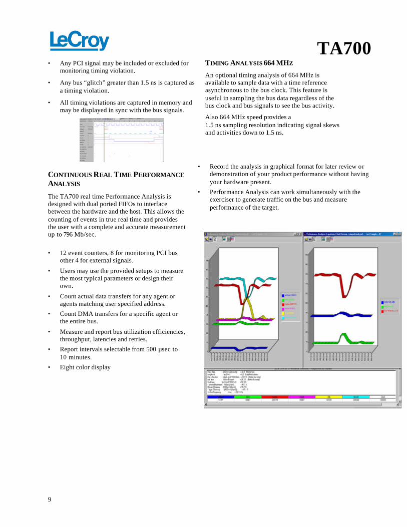
CONTINUOUS REAL TIME PERFORMANCE ANALYSIS
The TA700 real time Performance Analysis is designed with dual ported FIFOs to interface between the hardware and the host. This allows the counting of events in true real time and provides the user with a complete and accurate measurement up to 796 Mb/sec.
• 12 event counters, 8 for monitoring PCI bus
other 4 for external signals.
• Users may use the provided setups to measure the most typical parameters or design their own.
• Count actual data transfers for any agent or agents matching user specified address.
• Count DMA transfers for a specific agent or the entire bus.
• Measure and report bus utilization efficiencies, throughput, latencies and retries.
• Report intervals selectable from 500 µsec to 10 minutes.
• Eight color display
• Record the analysis in graphical format for later review or demonstration of your product performance without having your hardware present.
• Performance Analysis can work simultaneously with the exerciser to generate traffic on the bus and measure performance of the target.
TA700
10
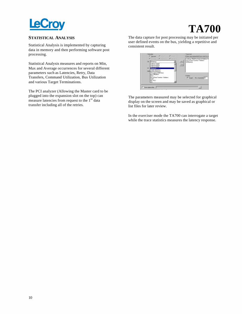
STATISTICAL ANALYSIS Statistical Analysis is implemented by capturing data in memory and then performing software post processing.
Statistical Analysis measures and reports on Min, Max and Average occurrences for several different parameters such as Latencies, Retry, Data Transfers, Command Utilization, Bus Utilization and various Target Terminations.
The PCI analyzer (Allowing the Master card to be plugged into the expansion slot on the top) can measure latencies from request to the 1st data transfer including all of the retries.
The data capture for post processing may be initiated per user defined events on the bus, yielding a repetitive and consistent result.
The parameters measured may be selected for graphical display on the screen and may be saved as graphical or list files for later review.
In the exerciser mode the TA700 can interrogate a target while the trace statistics measures the latency response.
TA700
11
EXERCISER The 66 MHz 64 bit exerciser operates as Master and Target, and is compliant in both 5V and 3.3V environments.
On board target memory allows testing read/write operation of master agents.
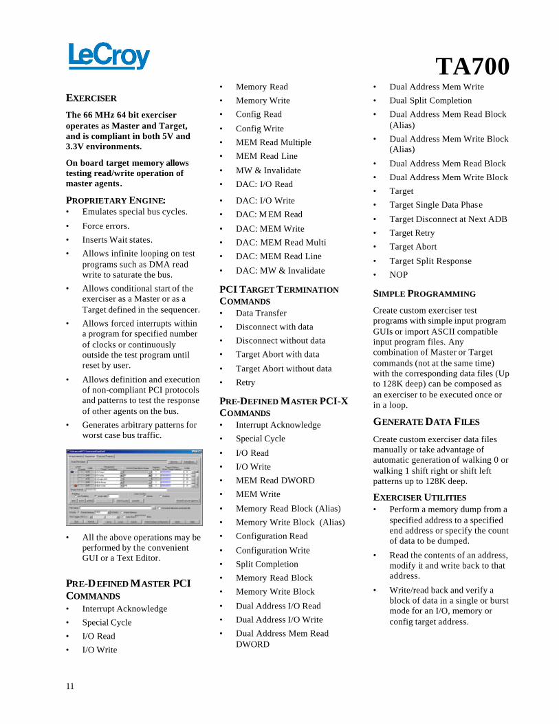
PROPRIETARY ENGINE: • Emulates special bus cycles.
• Force errors.
• Inserts Wait states.
• Allows infinite looping on test programs such as DMA read write to saturate the bus.
• Allows conditional start of the exerciser as a Master or as a Target defined in the sequencer.
• Allows forced interrupts within a program for specified number of clocks or continuously outside the test program until reset by user.
• Allows definition and execution of non-compliant PCI protocols and patterns to test the response of other agents on the bus.
• Generates arbitrary patterns for worst case bus traffic.
• All the above operations may be performed by the convenient GUI or a Text Editor.
PRE-DEFINED MASTER PCI COMMANDS • Interrupt Acknowledge
• Special Cycle
• I/O Read
• I/O Write
• Memory Read
• Memory Write
• Config Read
• Config Write
• MEM Read Multiple
• MEM Read Line
• MW & Invalidate
• DAC: I/O Read
• DAC: I/O Write
• DAC: M EM Read
• DAC: MEM Write
• DAC: MEM Read Multi
• DAC: MEM Read Line
• DAC: MW & Invalidate
PCI TARGET TERMINATION COMMANDS • Data Transfer
• Disconnect with data
• Disconnect without data
• Target Abort with data
• Target Abort without data
• Retry
PRE-DEFINED MASTER PCI-X COMMANDS • Interrupt Acknowledge
• Special Cycle
• I/O Read
• I/O Write
• MEM Read DWORD
• MEM Write
• Memory Read Block (Alias)
• Memory Write Block (Alias)
• Configuration Read
• Configuration Write
• Split Completion
• Memory Read Block
• Memory Write Block
• Dual Address I/O Read
• Dual Address I/O Write
• Dual Address Mem Read DWORD
• Dual Address Mem Write
• Dual Split Completion
• Dual Address Mem Read Block (Alias)
• Dual Address Mem Write Block (Alias)
• Dual Address Mem Read Block
• Dual Address Mem Write Block
• Target
• Target Single Data Phase
• Target Disconnect at Next ADB
• Target Retry
• Target Abort
• Target Split Response
• NOP
SIMPLE PROGRAMMING
Create custom exerciser test programs with simple input program GUIs or import ASCII compatible input program files. Any combination of Master or Target commands (not at the same time) with the corresponding data files (Up to 128K deep) can be composed as an exerciser to be executed once or in a loop.
GENERATE DATA FILES
Create custom exerciser data files manually or take advantage of automatic generation of walking 0 or walking 1 shift right or shift left patterns up to 128K deep.
EXERCISER UTILITIES • Perform a memory dump from a
specified address to a specified end address or specify the count of data to be dumped.
• Read the contents of an address, modify it and write back to that address.
• Write/read back and verify a block of data in a single or burst mode for an I/O, memory or config target address.
TA700
12
• Scan Configuration Registers finds all PCI agents on the local and the secondary bus.
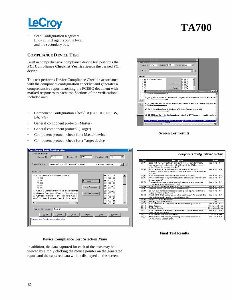
COMPLIANCE DEVICE TEST Built in comprehensive compliance device test performs the PCI Compliance Checklist Verification on the desired PCI device.
This test performs Device Compliance Check in accordance with the component configuration checklist and generates a comprehensive report matching the PCISIG document with marked responses to each test. Sections of the verifications included are:
• Component Configuration Checklist (CO, DC, DS, BS, BA, VG)
• General component protocol (Master)
• General component protocol (Target)
• Component protocol check for a Master device.
• Component protocol check for a Target device
Device Compliance Test Selection Menu
In addition, the data captured for each of the tests may be viewed by simply clicking the mouse pointer on the generated report and the captured data will be displayed on the screen.
Screen Test results
Final Test Results
TA700
13
TA700 COM API
A COM Object library included with your analyzer enables programmers to incorporate most of the TA700 functionality in their own programs developed on platforms such as Microsoft Visual C++, Borland Delphi and Microsoft Visual Basic.
The major components are:
♦ A project server interface that allows the user to run a predefined project.
♦ A change project server interface that allows the user to modify a predefined TA700 project.
♦ A utility server that allows the user to collect information from the TA700 board.
TA700
14
SPECIFICATIONS
ANALYZER
Bus Type
TA700-5 PCI – PCI-X, 5V Key
TA700-3 PCI – PCI-X, 3.3V Key
Bus width 32 or 64 bit wide
Maximum Clock Rate Up to 66 MHz, analyzer
Up to 100 MHz PCI-X
Up to 66 MHz, exerciser
Min 25 MHz
External Inputs
16 Channels Sampled in memory, may be used as trigger inputs or as input to performance analysis.
1 External Trigger Out Positive or negative TTL Level synchronized to the sequencer first time trigger.
Memory Depth per Channel
Trace, 95 PCI signals 128K
Trace, optional 4 Meg
External Signals 16 x 128K
Exerciser, 95 signals 128K
Protocol Errors 128K
Timing Errors 128K
Time Tag 128K
Word Recognizers 8 Event patterns.
Triggering Events Any of the 8 events, Boolean equation of the events, external input channels or trigger on timing or protocol errors.
30 - 20 bit Counters Used as 30 event or delay counters at each state.
32 Level Sequencer Supported at each level by Store, Set Trigger, Set Tag, Discard, If, Else If, GoTo, Delay Time, Delay Count and Start Exerciser statements.
Counter Use Count Accumulative Count & reset as High Pass filter for triggering on system crashes. Count & reset as Low Pass filter.
TIMING MEASUREMENT
Synchronous
Strobe Window strobe (2 edges)
Width 95 (64 bit PCI + control signals).
Resolution 100 Ps/edge
Operating Frequency 25 MHz to 66MHz
Spread 2-12 ns 33 MHz mode
2-5 ns 66 MHz mode
Glitch Detection 1.5 ns
Signals Any or all PCI bus signals may be included or masked individually.
Display Red flag on the data display for each PCI signal, identified by the PCI signal name.
Asynchronous
Clock 664 MHz
Width 64 bit (selectable for AD[00-31] or AD[32-63]
Resolution 1.5 ns
Memory Depth 512K
TA700
15
TIME TAG Counter 40 bits
Resolution 15 ns to 40 ns
Recording Duration up to 5 Hours at 15 ns, up to 10 Hours at 30 ns.
Reported display Absolute time from the start, Relative to trigger point, relative to each data sample, Latencies for Target and Master.
PERFORMANCE ANALYSIS
Real-time, Continuous
Event Counters 8 32 bit counters.
Count qualifier Every bus cycle, User defined address space or Sequencer (Based on user defined sequence of events)
Count Modes Reset or Accumulative
Count Interval 500 us to 10 minutes
Output Results Reports
Pre-defined Bus utilization, Efficiencies, Throughput, Latencies, DMA transfers, Idle time; I/O vs. Memory utilization.
Custom Per user defined equations.
Measurement Reports Normalized to largest per interval or Absolute measurement.
Output Display (real Time) Text Report, Bar Graph, Pie Chart and histogram.
Display Modes Color; 2D or 3D
Host CPU interface Real-time FIFOs
Blank
TA700
16
Statistical (Memory Capture)
Capture Depth User defined up to 128 K
Capture Qualifier User defined sequence of events.
Measurement types Min, Max or Average. Number of occurrences. Percentage of occurrences.
Measurement Qualifiers User-defined address, address range or cycle type.
Report Types Graphical and Text
Measured Parameters Latency Target
Latency Master
Latency Arbiter
Efficiency
Target Efficiency
Master Efficiency
Throughput Mb/Sec
Bus Utilization
IDLE
No of Data Transfer/Address
Wait
Int Ack
I/O
I/O RD
I/O WR
Memory
Mem RD
Mem WR
Configuration
CFG RD
CFG WR
MEM RM
Dual ADD
MEM RL
MEM W&I
Total No of Data
RETRY
TABORT
DIS+DATA
DIS-DATA
MABORT
Latency, REQ# to Data
TA700
17
UTILITIES Search By name, forward,
backward and for consecutively re-occurring patterns.
Post-capture filter Include or exclude user defined patterns.
Convert Captured Data ASCII
EXCEL
PCX
Compare Captured Data User defined start and end from each file .
Jump Within Display Jump in results display relative to X and Y, trigger positions from starting position.
Capture Screen Capture a mouse selectable screen area and save as a *.pcx file.
Zoom Zoom the display around X and Y cursors, between X and Y cursors or Zoom around independently of cursors.
MNEMONICS
100 User Defined per file May be saved for recall in a different application. Unlimited files may be generated and saved.
PCI Bus Inverse decode of all PCI initiator and target termination.
EXERCISER
Bus Width Up to 64 Bit
Bus Speed 25 to 66 MHz
Output Voltage Swing 3.3 V
Link To the Analyzer, Start after defined events, Start after external trigger
DATA BLOCK GENERATION • Data block generation of W1, W0 or user patterns.
• 8, 16, 32 or 64 bit wide.
• Up to 128K deep.
• Multiple blocks of data in to a single file.
• May be generated in the GUI and saved as ASCII format.
• May be generated in a text editor and imported to the exerciser program.
TA700
18
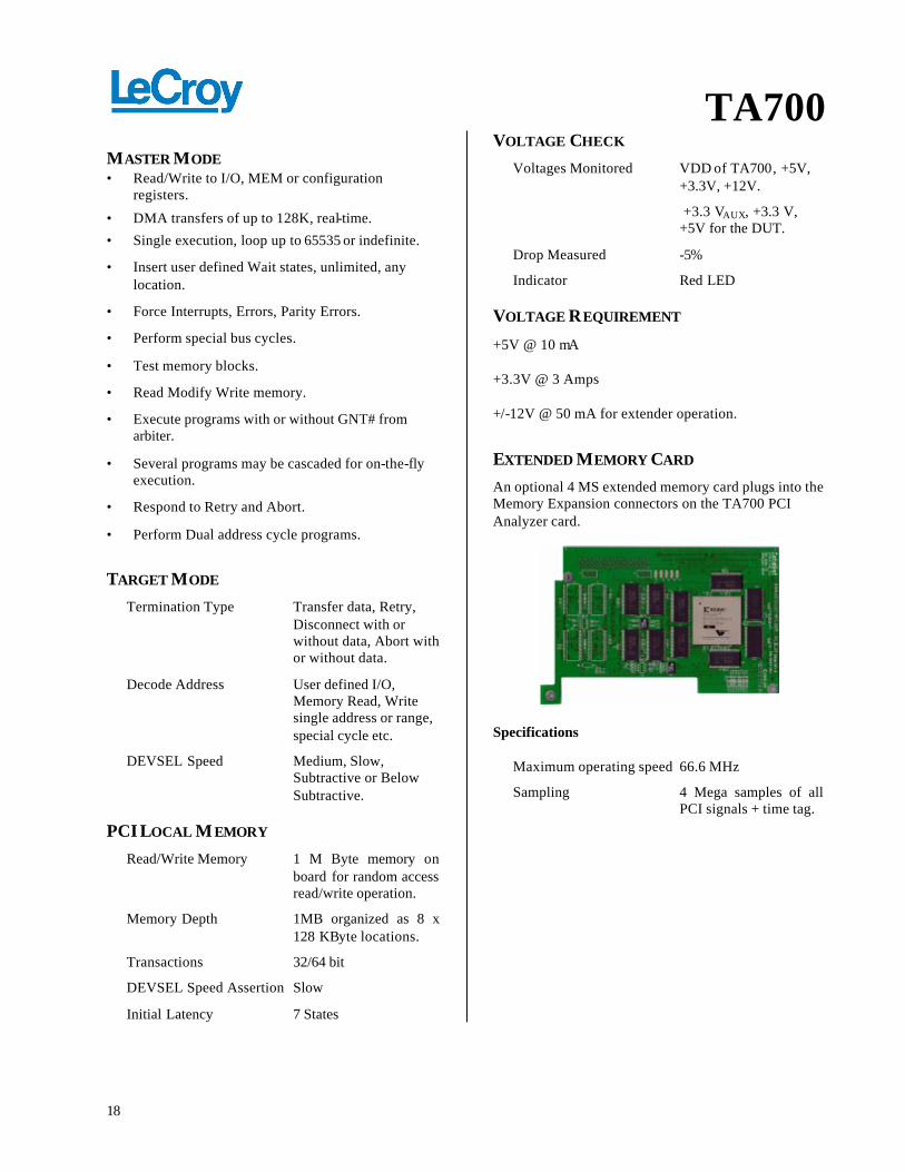
MASTER MODE • Read/Write to I/O, MEM or configuration
registers.
• DMA transfers of up to 128K, real-time.
• Single execution, loop up to 65535 or indefinite.
• Insert user defined Wait states, unlimited, any location.
• Force Interrupts, Errors, Parity Errors.
• Perform special bus cycles.
• Test memory blocks.
• Read Modify Write memory.
• Execute programs with or without GNT# from arbiter.
• Several programs may be cascaded for on-the-fly execution.
• Respond to Retry and Abort.
• Perform Dual address cycle programs.
TARGET MODE Termination Type Transfer data, Retry,
Disconnect with or without data, Abort with or without data.
Decode Address User defined I/O, Memory Read, Write single address or range, special cycle etc.
DEVSEL Speed Medium, Slow, Subtractive or Below Subtractive.
PCI LOCAL M EMORY Read/Write Memory 1 M Byte memory on
board for random access read/write operation.
Memory Depth 1MB organized as 8 x 128 KByte locations.
Transactions 32/64 bit
DEVSEL Speed Assertion Slow
Initial Latency 7 States
VOLTAGE CHECK Voltages Monitored VDD of TA700, +5V,
+3.3V, +12V.
+3.3 VAUX, +3.3 V, +5V for the DUT.
Drop Measured -5%
Indicator Red LED
VOLTAGE REQUIREMENT
+5V @ 10 mA
+3.3V @ 3 Amps
+/-12V @ 50 mA for extender operation.
EXTENDED MEMORY CARD An optional 4 MS extended memory card plugs into the Memory Expansion connectors on the TA700 PCI Analyzer card.
Specifications
Maximum operating speed 66.6 MHz
Sampling 4 Mega samples of all PCI signals + time tag.