110 THYRISTOR PROJECTS using SCRs and TRIACS
78
110 THYRISTOR PROJECTS using SCRs and TRIACS R.M. Marston È Meniti Ttthrilcd Book
Transcript of 110 THYRISTOR PROJECTS using SCRs and TRIACS
110 THYRISTOR PROJECTS using SCRs and TRIACS
R.M. Marston
È Meniti Ttthrilcd Book

110 Thyristor Projects using S.C.R.s and Triacs

Other Books by R.M. Marston
20 Solid State Projects for thè Home 20 Solid State Projects for thè Car and Garage 110 Semiconductor Projects for thè Home Constructor 110 Integrated Gircuit Projects for thè Home Constructor
110 Thyristor Projects using S.C.R.s and Triacs
R.M. MARSTON
THE BUTTERWORTH GROUP
ENGLAND: Butterworth & Co (Publishers) Ltd London : 88 Kingsway, WC2B 6AB
AUSTRALIA : Butterworths Pty Ltd Sydney: 586 Pacific Highway Chatswood, NSW 2067 Melbourne: 343 Little Collins Street, 3000 Brisbane: 240 Queen Street, 4000
CANADA: Butterworth & Co (Canada) Ltd Scarborough: 2265 Midland Avenue, Ontario M1P 4SI
NEW ZEALAND: Butterworths of New ZeaJand Ltd Wellington: 26-28 Waring Taylor Street, 1
SOUTH AFRICA : Butterworth & Co (South Africa) (Pty) Ltd Durban: 152-154 Gale Street
First published in 1972 by Newnes Technical Books Second impression 1975
© R. M. Marston, 1972
All rights reserved. No part of this publication may be reproduced or transmitted in any form or by any means, including photo- copying and record ing, without thè written permission of thè copy¬ right holder, application for which should be addressed to thè publisher. Such written permission must also be obtained before any part of this publication is stored in a retrieval System of any nature.
This book is sold subject to thè Standard Conditions of Sale of Net Books and may not be sold in thè U.K. below thè net pricé given by thè publishers in tfieir current price list.
ISBN 0 592 00074 5 Limp
Printed in England by Billing & Sons Limited, Guildford and London
PREFACE
S.C.R.s and triacs are high-speed solid-state power switches. They can operate at potentials up to hundreds of volts, and can handle currents
up to tens or hundreds of amps. They have a multitude of applications
in thè home and in industry, and can readily be used to control electric lamps, motors, heaters and alarms.
This book is intended to be of equal interest to thè electronics amateur, student and engineer. With this aim in mind, thè volume starts off by outlining thè essential operating characteristics of thè s.c.r. and thè triac, and then goes on to show 110 useful projects in which these devices can be used. All of these projects have been designed, built and fully evaluated by thè author, and range from simple electronic alarms to highly sophisticated self-regulating electric-heater power controller. Many of thè projects use advanced design concepts, and are of outstand- ing technical interest. The operating principle of each project is explained in concise but comprehensive terms, and brief constructional notes are given where necessary.
All of thè projects are designed around internationally available components. The semiconductors used are of American manufacture, but are readily available in all parts of thè western world. The volume is specifìcally designed to be of equal interest to both American and English readers. Where applicable, alternative component values are given for use on both 120 V and 240 V power lines, thè 240 V values being noted in parentheses in thè appropriate Circuit diagrams. The outlines of all semiconductors used in thè projects are given in thè appendix, as an aid to construction. Unless otherwise stated, all resistors used in thè projects are standard half-watt types.
R. M. Marston

CONTENTS
1 Basic Principles and Projects ]
2 15 A.C. Power-Switching Projects 23
3 20 Electronic Alarm Projects 33
4 15 Time-Delay Projects 54
5 25 Lamp-Control Projects 53
6 15 Heater-Control Projects 94
7 15 Universal-Motor Control Projects HO
8 5 Miscelianeous Projects 123
Appendix 132
Index 135

CHAPTER 1
BASIC PRINCIPLES AND PROJECTS
S.C.R.s and triacs are members of thè thyristor family. They act as high- speed power switches. They are solid-state devices, and can operate at
potentials up to several hundred volts, and can handle currents up to tens or hundreds of amps. They can be used to replace conventional mechanical switches and relays in many d.c. and a.c. power control Systems, and can readily be used to control electric lamps, motors, heaters and alarms. They have a multitude of uses in thè home and in industry.
This chapter explains thè basic characteristics of these outstandingly useful devices, and shows a selection of basic circuits in which they can be used for demonstration and educational purposes.
The s.c.r.: basic theory
The s.c.r., or Silicon controlled rectifier, is a four-layer pnpn Silicon semiconductor device, and is represented by thè symbol shown in
Figure Lia. Note that this symbol resembles that of a normal rectifier, but has an additional terminal known as thè ‘gate’. The s.c.r. can be made to act as either an open-circuit switch or as a Silicon rectifier, depending on how its gate is used.
Figure l.lb shows thè transistor equivalent Circuit of thè s.c.r. Essentially, thè Circuit is that of a complementary regenerative switch, in which thè collector current of npn transistor Q\ feeds directly into thè base of pnp transistor Q2 and thè collector current of Q2 feeds into thè base of gì- This equivalent Circuit is of great value in understanding s.c.r. characteristics.
1
2 BASIC PRINCIPLES AND PROJECTS
Figure l.lc shows thè basic connections for using thè s.c.r. as a switch in d.c. circuits. The load is connected in series with thè s.c.r. anode and cathode and is connected across thè supply so that thè anode
Figure 1.1 a Figure l.lb Figure Llc
S.C.R. symbol. Transistor equivalent circuii of thè s.c.r. Basic connections for using thè s.c.r. as a d.c. switch.
is positive relative to thè cathode. The gate can be connected to thè
positive supply line via R i and S2 ■ The basic characteristics of thè s.c.r. can be readily understood by
referring to Figures Llb and l.lc, and are as follows. (1) . When power is first applied to thè s.c.r. (by closing Sx in
Figure Llc) thè s.c.r. is ‘blocked’, and acts (between anode and cathode) like an open-circuit switch. Looking at Figure Llb it can be seen that this action is due to thè fact that Q1 base is shorted to thè cathode via R i and R2, so Qi is cut off and passes negligible collector current into thè base of Q2, which is hence also cut off and passes negligible current into Q1 base. Both transistors are thus cut off under
this condition, and only a small leakage current flows between thè
anode and cathode of thè device. (2) . The s.c.r. can be turned on and made to act like a normal
Silicon rectifìer by applying a positive current to thè gate by closing ^2- When this gate current is applied thè s.c.r. regenerates and turns on very rapidly, and thè full load current flows between thè anode and cathode. As in thè case of a normal Silicon rectifìer, a saturation potential of one or two volts is developed between thè anode and cathode of thè s.c.r. when it is on. Referring to Figure Llb, these
characteristics can be explained as follows. When thè gate is made positive with respect to thè cathode, gate
current flows via R2 and via R i and thè base-errtitter junction of Qi. If thè gate current is sufficienti large Q i is biased on and its collector current feeds into thè base of Q2. This base current is amplified by Q2
BASIC PRINCIPLES AND PROJECTS 3
and is fed back into thè base of Ql} where it is again amplified and fed to Q2. A regenerative action thus takes place, and both transistors switch rapidly into saturation. Under this condition thè anode-to- cathode saturation voltage is equal to thè sum of thè Q2 saturation voltage and thè Ql forward base-emitter voltage, and amounts to one or two volts. Modern s.c.r.s have typical turn-on times of a few
microseconds. (3) . Once thè s.c.r. has been turned on and is conducting in thè
forward direction thè gate loses control, and thè s.c.r. then remains on even if thè gate drive is completely removed. Thus, only a brief positive
gate pulse is needed to turn thè s.c.r. on. Considerable current gain is available between thè gate and anode of thè device, so very small amounts of gate power can be used to control very high power values in thè external load.
The above points should be self-evident from Figure Llb. A small drive current must be fed into thè base of 2i via R i and thè gate terminal to cause thè Circuit to regenerate initially, bui once regenera¬ tion is complete thè Ql base drive necessary to sustain thè Circuit in thè saturated state is provided via Q2 collector, so thè Circuit self- latches and remains on even when thè gate drive is removed. R i ensures that base current continues to flow in even if thè gate-cathode terminals are shorted or reverse biased, so thè gate loses all control
once thè Circuit has switched into thè self-latching mode. Since Qi and Q2 are connected as a positive feedback network they
produce a combined loop gain equal to thè product of their individuai gains. Typically, s.c.r.s give current gains, between gate and anode, of thè order of one thousand times. Milliamps of gate current can be used to control amps of anode current. The gate of thè s.c.r. has non-linear characteristics similar to those of thè base of a normal Silicon transistor (as is self-evident from Figure Llb), and gate potentials of thè order of one volt are suffìcient to turn thè s.c.r. on. S.c.r.s can be used to switch potentials up to several hundred volts, so high voltage gains are available from thè device. Thus, extremely high power (volts x amps) gains are available from s.c.r.s, and milliwatts of gate power can be used to
control kilowatts of load power. (4) . Once thè s.c.r. has self-latched into thè on state it can only be
turned off again by momentarily reducing its anode current to zero, or below a value known as thè ‘minimum holding current’. Since tum-off occurs whenever thè current is reduced below this criticai value, it follows that turn-off occurs automatically in a.c. circuits near thè zero- crossing point at thè end of each half-cycle. The fact that turn-off occurs when thè main current falls below a minimum holding value, rather than to zero, is due to thè fact that thè current gains of thè two transistors in thè Figure Llb Circuit fall off as thè anode current is
4 BASIC PRINCIPLES AND PROJECTS
reduced, and thè Circuit unlatches when thè anode current falls to such a low value that thè combined loop gain of thè two transistors falls below unity. Minimum holding current values are typically of thè order of a few milliamps.
(5). A certain amount of internai capacitance exists between thè anode and gate of thè s.c.r. Consequently, if a sharply rising voltage is applied to thè s.c.r.s anode this internai capacitance can cause part of thè rising anode signal to break through to thè gate and thus trigger thè s.c.r. on. This ‘rate-effect’ turn-on can be caused by supply-line transients, and sometimes occurs at thè moment that supplies are
switch-connected to thè s.c.r. anode. Rate-effect problems can usually be overcome by wiring a simple R — C smoothing network between thè
anode and cathode of thè s.c.r., to limit thè rate of rise to a safe value.
The s.c.r.: basic d.c. circuits
Having examined thè basic characteristics of thè s.c.r. we can now go on to look at a few basic circuits that can be used to demonstrate these characteristics in a practical way.
Figure 1.2a shows a simple d.c. on-off Circuit controlling a 12 V 500 mA lamp. The lamp can be replaced with an alternative type of
Figure L2a Simple d.c. on-off Circuit. Figure L2b Alternative d.c. on-off Circuit.
load if required, but if an inductive load is used it must be shunted by a damping diode (Z^), so that thè Circuit is not damaged by back e.m.f.s as thè s.c.r. is switched on or off. The s.cj. used here can handle anode currents up to 2 A, and can be turned on by gate currents as low as a few hundred microamps. Gate current is provided via limiting resistor/?! and push-button switch SV R2 is wired between thè s.c.r.s gate and cathode to improve Circuit stability, in thè same way as a resistor may
BASIC PRINCIPLES AND PROJECTS 5
be wired between thè base and emitter of a conventional transistor for thè same purpose.
The Figure 1.2a Circuit can be turned on by briefly closing^!. Once thè Circuit has been turned on it self-latches and stays on when Sv is opened again. The Circuit can be turned off by momentarily reducing thè anode current to zero by opening S2. Alternatively, thè Circuit can be turned off by momentarily applying a short between thè s.c.r.s anode and cathode, as shown in Figure L2b.
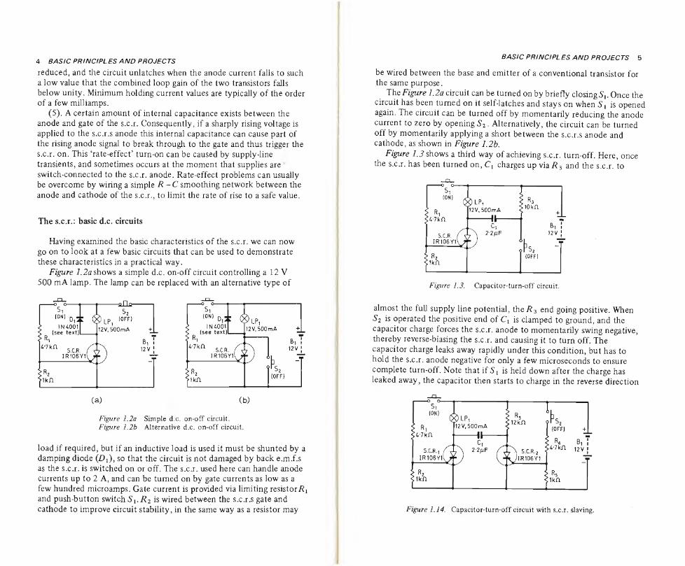
Figure 1.3 shows a third way of achieving s.c.r. turn-off. Here, once thè s.c.r. has been turned on, Cy charges up via /?3 and thè s.c.r. to
Figure 1.3. Capacitor-turn-off Circuit.
almost thè full supply line potential, thè /?3 end going positive. When
S2 is operated thè positive end of C\ is clamped to ground, and thè capacitor charge forces thè s.c.r. anode to momentarily swing negative, thereby reverse-biasing thè s.c.r. and causing it to turn off. The capacitor charge leaks away rapidly under this condition, but has to hold thè s.c.r. anode negative for only a few microseconds to ensure
complete turn-off. Note that if S\ is held down after thè charge has leaked away, thè capacitor then starts to charge in thè reverse direction
Figure 1.14. Capacitor-turn-off Circuit with s.c.r. slaving.
6 BASIC PRINCIPI. ES AND PROJECTS
via thè lamp load: Cl must thus be a non-polarised type, such as
Mylar or polyester. A variation of thè capacitor turn-off Circuit is shown in Figure 1.4.
Here a slave s.c.r. is used to replace S2 of Figure 13, and capacitive
turn-off of SCRl is achieved by briefly driving SCR 2 on via a low- current pulse from S2. SCR2 turns off once S2 is released, since thè anode current provided by R$ is lower than thè SCR2 holding current.
Figure L5 shows thè Circuit of an s.c.r. bistable or flip-flop driving two independent lamp loads. Assume that SCRl is on and SCR2 is off,
Figure 1.5. S.C.R. bistable or flip-flop.
so that Ci (non-polarised) is fully charged with its LP2 end positive. The state of thè Circuit can be changed by momentarily operating S2. SCR2 is then driven on via its gate, and as it goes on it drives SCRl off capacitively via its anode. Ci then recharges in thè reverse direction. Once recharging is complete thè state of thè Circuit can again be changed by briefly operating Sl, thus driving SCR i on via its gate and driving SCR2 off capacitively via its anode. The flip-flop process can be
repeated ad infinitum. All thè d.c. circuits that we have looked at so far have used simple
fìxed loads, and have thus been of thè self-latching type. Figure L6ay however, shows a simple d.c. alarm Circuit driving a self-interrupting load such as a bell, buzzer, or siren. When self-interrupting devices such as these are connected across a supply a current flows thxough a built-in
solenoid via a pair of contacts; this current induces a magnetic fìeld in thè solenoid, and causes a striker to fly outwards and open thè contacts, causing thè current to fall to zero and making thè magnetic field collapse. Once thè fìeld has collapsed thè striker falls back again and thè contacts dose, so current is again applied to thè solenoid and thè action repeats.
Consequently, this type of load acts like a switch that repetitively opens and closes rather rapidly. When such loads are connected in thè Figure L6a Circuit, therefore, thè Circuit does not self-latch in thè
BASIC Pfì/NC/PL ES AND PROJECTS 1
normal way, and thè alarm operates only so long as Si is closed. Due to thè inductive nature of such loads a damping diode must be wired across them when they are used in s.c.r. circuits, as shown in thè diagram.
The alarm circuits can be made to self-latch, if required, by simply wiring a 470-ohm resistor in parallel with thè alarm, as shown in
Figure 1.6a. Simple non-latching Figure 1.6b. Simple self-latching alarm Circuit. alarm Circuit.
Figure L6b. In this case thè anode current of thè s.c.r. does not fall to zero when thè alarm self-interrupts, but falls to a value dietated by Rs and thè battery voltage. If this current is in excess of thè s.c.r.s holding current thè s.c.r. self-latches. The Circuit can be unlatched by briefly operating S2, so that thè anode current falls to zero when thè alarm enters a self-interrupting stage, and thè s.c.r. turns off.
The actual alarm used in thè Figure 1.6 circuits can be any low- voltage (3 to 12 V) self-interrupting bell, buzzer, or siren that draws an operating current of less than 2 A. The supply battery should give a voltage roughly 1*5 V greater than thè normal operating voltage of thè alarm device, to compensate for thè saturation voltage that is *lost’ across thè s.c.r. when it is on.
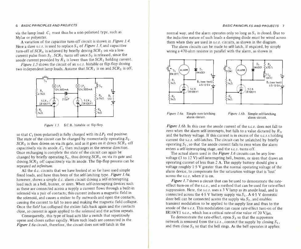
Figure 1.7 shows a Circuit that can be used to demonstrate thè rate- effect turn-on of thè s.c.r., and a method that can be used for rate-effect suppression. Here, thè s.c.r. uses a 3 V lamp as its anode load, and is connected across thè 4-5 V battery supply via Sr. A 4-5 V domestic door bell can be connected across thè supply via S2, and enables
transient modulation to be applied to thè supply line and thus to thè
anode of thè s.c.r. This modulation can cause rate-effect turn-on of thè IR106Y1 s.c.r., which has a criticai rate-of-rise value of 20 V/jus.
To demonstrate thè rate-effect, open S3 so that thè suppressor network is removed from thè s.c.r., connect thè supply by closing Sx, and then dose S2 so that thè bell rings. As thè bell operates it applies
8 BASIC PR/NCIPLES AND PROJECTS
high transient modulation to thè positive supply line, and this modula- tion appears at thè s.c.r. anode and should trigger thè s.c.r. and thè lamp on. If thè lamp does not go on, it may be that thè battery has a low internai resistance. If so, try connecting a 0-5-ohm resistor in series with
Figure 1.7. Rate-effect demonstration Circuit.
thè battery, so that thè correct operation is obtained. Once thè s.c.r. and lamp have been triggered on by rate-effect they can be turned off again by briefly opening Si.
Once thè turn-on rate-effect has been demonstrated thè effects of thè suppressor network can be shown by closing S3 and operating thè bell
again via S2. When S3 is closed thè lamp resistance and Cx act as a smoothing network that reduces thè rate-of-rise of thè anode modula¬ tion signal to a safe value, and thè s.c.r. does not go on when thè bell operates. If thè s.c.r. stili goes on under this condition, increase thè Ci value until thè correct results are obtained. Ci charges to thè full supply line potential when Si is closed, and R2 is wired in series with Cx to limit its discharge current into thè s.c.r. anode to a safe value. Di makes R2 appear as a Virtual short-circuit to sharply rising anode signals, however, so R2 does not effect thè time Constant of thè R-C rate-effect suppression network formed by Cj and thè lamp resistance. In many application D\ can be eliminated from thè suppressor Circuit.
The s.c.r.: basic a.c. circuits
Figure 1.8shows a basic half-wave a.c. on-off Circuit driving a 100 W lamp from a 120 V or 240 V a.c. power line. With Si open zero drive is
applied to thè s.c.r. gate, so thè s.c.r. and lamp are off. Suppose, however, that Si is closed. At thè start of each positive half-cycle thè s.c.r. is off, so thè full available line voltage is applied to thè gate via thè lamp and D\ and R ]. Shortly after thè start of thè half-cycle suffìcient voltage is
BASIC PRINCIPI. ES AND PROJECTS 9
available to trigger thè s.c.r., and thè s.c.r. and lamp go on. As thè s.c.r goes on its anode voltage falls to near zero, thus removing thè gate drive current. Since a substantial anode current is flowing in thè s.c.r. at this time, however, thè s.c.r. remains fully latched on for thè duration of thè half-cycle. The s.c.r. automatically turns off when thè half-cycle ends and thè anode current falls to zero.
This process repeats, with thè s.c.r. triggering on shortly after thè start of each positive half-cycle, so long as Sx is closed, and half-wave
power is applied to thè lamp. The s.c.r. and lamp turn off when S\ is
re-opened, since s.c.r. turn-off occurs automatically at thè end of each positive half-cycle.
Diode D\ in this Circuit prevents reverse bias being applied to thè s.c.r. gate on negative half-cycles of line voltage. Rx is given a low value so that thè s.c.r. can be turned on as early as possible in each positive half-cycle, but is large enough to limit thè peak gate current to a safe value in thè event of Si first being closed when thè instantaneous line voltage is at its peak value. Note that although very high peak voltage and
and current values may be applied to R i, they are applied for only thè few microseconds that thè s.c.r. takes to turn on; thè mean power dissipation ofA is thus quite low, and this component can safely be given a half-watt rating.
S.C.R.s can be used in a variety of ways to give full-wave a.c. control. In Figures 1.9 and 1.10 thè a.c. is converted to rough (unsmoothed) d.c. via thè bridge rectifier D\ —A, and thè rough d.c. is applied to thè
s.c.r. With Si open thè s.c.r. is off, so zero current flows through thè bridge and thè load. When Sx is closed thè s.c.r is driven on shortly
after thè start of each half-cycle of rough d.c., and full-wave power is applied to thè load. As thè s.c.r. goes on in each half-cycle thè gate drive is automatically removed, but thè s.c.r. stays latched on for thè
duration of èach half-cycle, as already described. The s.c.r. switches off

10 BASIC PR/NC/PLESAND PROJECTS
automatically at thè end of each half-cycle as its anode current falls to zero, so power is automatically removed from thè load when Si is
opened.
Note in thè Figure 1.9 Circuit that thè load is connected in thè d.c. side of thè bridge, and thè Circuit is thus used to drive a d.c. load. A fuse
Figure 1.9. Full-wave on-off Circuit with a d.c. load. = 3A 200 p.i.v. Silicon rectifiers.
(3A 400 p.i.v. Silicon rectifiers.)
is placed in thè a.c. side of thè bridge to give protection in thè event of a
failure of one or more of thè bridge components. In thè Figure LIO circuit thè load is placed in thè a.c. side of thè bridge, so thè Circuit is used to control an a.c. load. A fuse is not required in this case, since thè load itself limits current to a safe value in thè event of a component
failure.
Figure Ì.10. Full-wave on-off circuit with a.c. load. £>1—D4 = 3A 200 p.i.v. Silicon rectifiers.
(3A 400 p.i.v. Silicon rectifiers.)
Finally, Figure 1.11 shows how two s.c.r.s can be connected in
inverse parallel to give direct full-wave switching of thè load. With Si open zero gate drive is applied to either s.c.r., so zero power is applied to thè load. When 5! is closed gate current is applied to SCR ion positive half-cycles via Di and R2, and SCR i is driven on. On negative
BASIC PRINCIPL ES AND PROJECTS 11
Figure 1.11. Full-wave line switch using two s.c.r.s.
half-cycles gate drive is applied to SCR2 via A and R2 , and SCR2 is driven on. Full-wave control is thus obtained.
The triac: basic principles and projects
S.C.R.S are unidirectional thyristor devices. They pass current in one
direction only, from anode to cathode. Triacs are also members of thè thyristor family, but are bidirectional devices. They can pass current in either direction. For most practical purposes a triac can be regarded as two conventional s.c.r.s connected in inverse parallel within a single three-terminal package, but so arranged that thè two s.c.r.s share a single gate terminal. The triac can be used as a solid-state power switch that is normally off but can be turned on via a suitable gate signal.
Figure 1.12a shows thè symbol that is used to represent thè triac, and.Figure 1.12b shows a basic connection for using thè device as an
a.c. power switch. The load is wired in series with thè triacs main
Figure 1.12a. Triac symbol. Figure 1.12b. Basic triac switching circuii with d.c.
gate drive.
12 BASIC PRINCIPLES AND PROJECTS
terminals, and thè series combination is wired directly across thè a.c. power line*. D.C. gate drive can be applied to thè triac by closing Sx.
The triac exhibits characteristics very similar to those of a pair of
s.c.r.s connected in inverse parallel. Referring to Figure 1.12b, these
characteristics are as follows. (1) . Normally, with no gate signal applied, thè triac is off and acts
(between MT\ and MT2) like an open-circuit switch. It passes negli¬ gile current in either direction, and zero power is applied to thè load.
(2) . UMT2 is appreciably positive or negative relative toMTi thè
triac can be turned on (so it acts like a closed switch between MT\ and MT2) by applying a suitable trigger or bias signal to its gate via Si. The device takes only a few microseconds to switch fully on.
(3) . Once thè triac has been turned on via its gate it self-latches, and remains on so long as main-terminal currents continue to flow. Only a brief pulse of gate current is thus needed to turn thè triac on.
(4) . Once thè triac has self-latched thè gate loses control and thè device can only be turned off again by momentarily reducing its main-
terminal currents below a near-zero minimum holding value. When +he
triac is used as an a.c. power switch, therefore, tum-off occurs auto- matically at thè zero-crossing point at thè end of each half-cycle as thè
main-terminal currents fall to zero. (5) . A saturation potential of one or two volts is developed across thè
triacs main-terminals when thè device is switched into thè on state. Thus
if thè triac is used to switch a 10 A load from a 240 V r.m.s. supply, and thè triac has a saturation potential of 1 *5 V, approximately 2 400 W can be switched by thè triac, but only 15 W are ‘lost’ in thè triac itself: This 15 W can be readily dissipated by connecting thè triac to a suitable heat sink. The triac thus makes an efficient a.c. power switch.
(6) . The triac can be turned on by either a positive or a negative gate signal, irrespective of thè polarities of thè main-terminal voltages. The device thus has four possible triggering modes, signified as follows:
I+ Mode = MT2 current +ve, Gate current +ve. l’Mode = ” ” +ve, ” ” -ve.
Ili+ Mode = ” ” -ve, ” ” +ve. Ili" Mode = ” ” -ve, ” ” -ve.
The gate sensitivities in thè I+ and IH" modes are relatively high, and
are approximately equal. The sensitivities in thè I” and III+ modes are also roughly equal to one another in modern triacs, but are only about half as great as in thè I+ and III” modes. The gate exhibits non-linear characteristics similar to those of thè s.c.r. Gate potentials of one or two volts and currents of a few tens of milliamps are sufficient to turn on a triac and control several amps of load current. Considerable power gain
is thus available between thè triac gate and thè load.
BASIC PRINCIPLES AND PROJECTS 13
Having examined thè basic characteristics of thè triac we can now go on to look at a few basic switching circuits that can be used to
demonstrate these characteristics in a practical way.
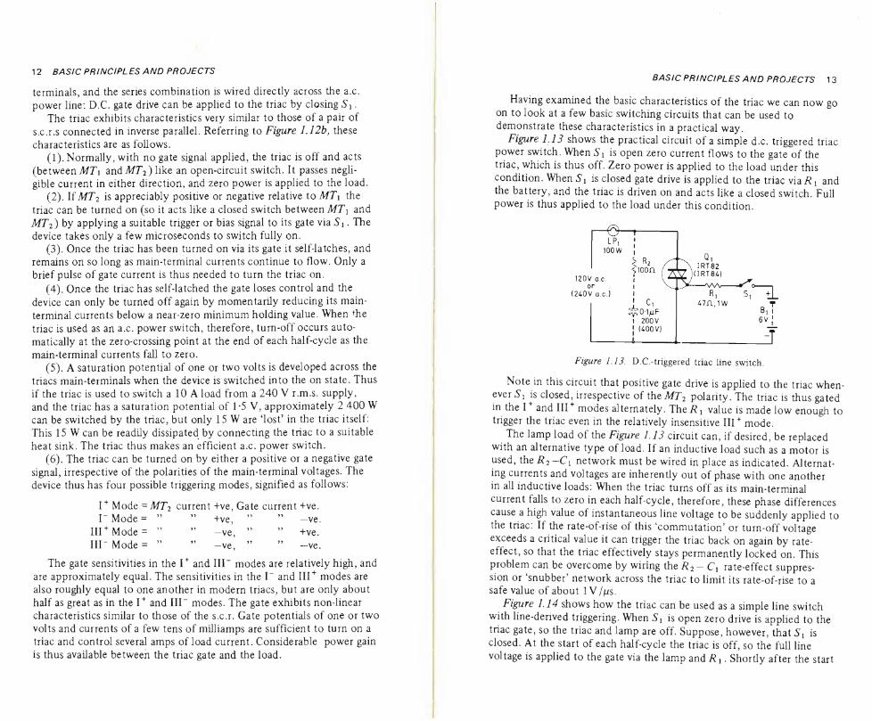
Figure 1.13 shows thè practical Circuit of a simple d.c. triggered triac power switch. When Si is open zero current flows to thè gate of thè triac, which is thus off. Zero power is applied to thè load under this
condition. When5i is closed gate drive is applied to thè triac via Ri and thè battery, and thè triac is driven on and acts like a closed switch. Full power is thus applied to thè load under this condition.
Figure 1.13. D.C.-triggered triac line switch.
Note in this Circuit that positive gate drive is applied to thè triac when- ever Si is closed, irrespective of theMT2 polarity. The triac is thus gated in thè I and III modes alternately. The R ! value is made low enough to trigger thè triac even in thè relatively insensitive III+ mode.
The lamp load of thè Figure 1.13 Circuit can, if desired, be replaced with an alternative type of load. If an inductive load such as a motor is used, thè R2 ~CX network must be wired in place as indicated. Alternat- ing currents and voltages are inherently out of phase with one another in all inductive loads: When thè triac turns off as its main-terminal
current falls to zero in each half-cycle, therefore, these phase differences cause a high value of instantaneous line voltage to be suddenly applied to
thè triac: If thè rate-of-rise of this ‘commutation’ or turn-off voltage exceeds a criticai value it can trigger thè triac back on again by rate- effect, so that thè triac effectively stays permanently locked on. This problem can be overcome by wiring thtR2-Cy rate-effect suppres- sion or ‘snubber’ network across thè triac to limit its rate-of-rise to a safe value of about 1V /jus.
Figure 1.14 shows how thè triac can be used as a simple line switch with line-derived triggering. When Si is open zero drive is applied to thè triac gate, so thè triac and lamp are off. Suppose, however, that Si is closed. At thè start of each half-cycle thè triac is off, so thè full line voltage is applied to thè gate via thè lamp and Ri. Shortly after thè start
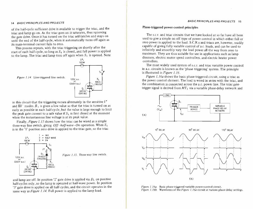
14 BASIC PRINCIPLES AND PROJECTS
of thè half-cycle sufficient drive is available to trigger thè triac, and thè triac and lamp go on. As thè triac goes on it saturates, thus removing thè gate drive. Once it has turned on thè triac self-latches and stays on until thè end of thè half-cycle, when it automatically turns off again as
its main-terminal current falls to zero. This process repeats, with thè triac triggering on shortly after thè
start of each half-cycle, so long as S\ is closed, and full power is applied to thè lamp. The triac and lamp turn off again when Si is opened. Note
Figure 1.14. Line-triggered line switch.
LPi 100W
in this Circuit that thè triggering occurs alternately in thè sensitive I + and III" modesti is given a low value so that thè triac is turned on as early as possible in each half-cycle, but thè value is large enough to limit thè peak gate current to a safè value if S{ is first closed at thè moment when thè instantaneous line voltage is at its peak value.
Finally, Figure 1.15 shows how thè triac can be wired as a simple three-way line switch, giving Off-half-wave-On operation. When Sx is in thè T position zero drive is applied to thè triac gate, so thè triac
1 = OFF LPi 2 = HALF-WAVE
100W 3 = ON
Figure 1.15. Three-way line switch.
and lamp are off. In position ‘2’ gate drive is applied via Di on positive half-cycles only, so thè lamp is operated at half-wave power. In position ‘3* gate drive is applied on all half-cycles, and thè Circuit operates in thè
same way as Figure 1.14. Full power is applied to thè lamp load.
BASIC PRINCIPE ES AND PROJECTS 15
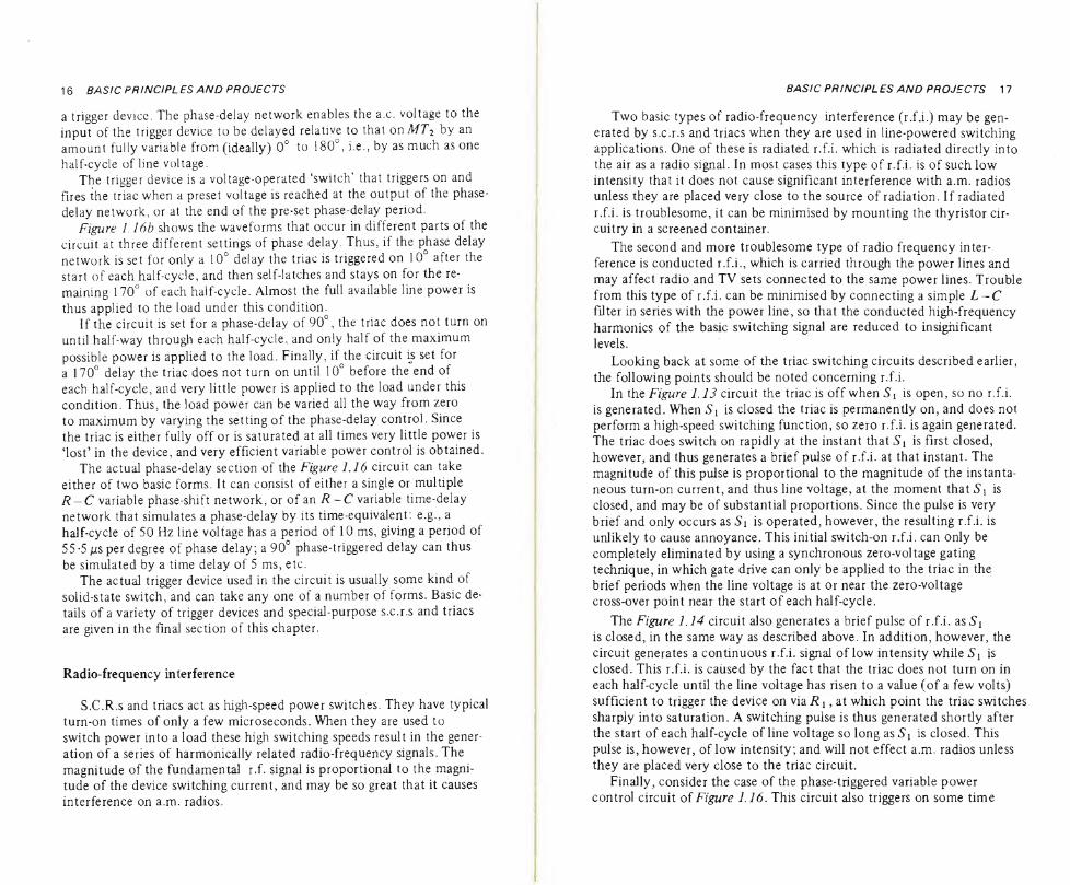
Phase-triggered power-control principies
The s.c.r. and triac circuits that we have looked at so far have all been used to give a simple on-off type of power control in which either full or zero power is applied to thè load. S.C.R.s and triacs are, however, readily capable of giving fully variable control of a.c. loads, and can be used to infinitely and smoothly vary thè load power all thè way from zero to maximum. They are thus suitable for use in application such as lamp
dimmers, electric motor speed controllers, and electric heater power controllers.
The most widely used System of s.c.r. and triac variable power control in a.c. circuits is known as thè ‘phase triggering’ System. The principle is illustrated in Figure 1.16.
Figure l.lóa shows thè basic phase-triggered Circuit, using a triac as thè power control element. The load is wired in series with thè triac, and thè combination is connected across thè a.c. power line. The triac gate-
trigger signal is derived ixomMT2 via a variable phase-delay network and
(b)
Figure LI6a. Basic phase-triggered variable power-control Circuit. Figure L16b. Waveforms of thè Figure l.lóa Circuit at various phase-delay settings.
16 BASIC PR/NC/PLES AND PROJECTS
a trigger device. The phase-delay network enables thè a.c. voltage to thè input of thè trigger device to be delayed relative to that on MT2 by an amount fuily variable from (ideally) 0° to 180°, i.e., by as much as one
half-cycle of line voltage. The trigger device is a voltage-operated ‘switch' that triggers on and
fires thè triac when a preset voltage is reached at thè output of thè phase- delay network, or at thè end of thè pre-set phase-delay period.
Figure 1. lób shows thè waveforms that occur in different parts of thè Circuit at three different settings of phase delay. Thus, if thè phase delay network is set for only a 10° delay thè triac is triggered on 10° after thè
start of each half-cycle, and then self-latches and stays on for thè re- maining 170° of each half-cycle. Almost thè full available line power is
thus applied to thè load under this condition. If thè circuit is set for a phase-delay of 90°, thè triac does not turn on
until half-way through each half-cycle, and only half of thè maximum
possible power is applied to thè load. Finally, if thè Circuit is set for a 170° delay thè triac does not turn on until 10° before thè end of each half-cycle, and very little power is applied to thè load under this condition. Thus, thè load power can be varied all thè way from zero to maximum by varying thè setting of thè phase-delay control. Since
thè triac is either fully off or is saturated at all times very little power is ‘lost’ in thè device, and very efficient variable power control is obtained.
The actual phase-delay section of thè Figure 1.16 Circuit can take either of two basic forms. It can consist of either a single or multiple R — C variable phase-shift network, or of an R-C variable time-delay network that simulates a phase-delay by its time-equivalent: e.g., a
half-cycle of 50 Hz line voltage has a period of 10 ms, giving a period of 55*5 fis per degree of phase delay; a 90° phase-triggered delay can thus
be simulated by a time delay of 5 ms, etc. The actual trigger device used in thè circuit is usually some kind of
solid-state switch, and can take any one of a number of forms. Basic de- tails of a variety of trigger devices and special-purpose s.c.r.s and triacs
are given in thè final section of this chapter.
Radio-frequency interference
S.C.R.s and triacs act as high-speed power switches. They have typical
turn-on times of only a few microseconds. When they are used to switch power into a load these high switching speeds result in thè gener¬
ation of a series of harmonically related radio-frequency signals. The magnitude of thè fundamental r.f. signal is proportional to thè magni- tude of thè device switching current, and may be so great that it causes
interference on a.m. radios.
BASIC PR/NC/PLES AND PROJECTS 17
Two basic types of radio-frequency interference (r.f.i.) may be gen- erated by s.c.r.s and triacs when they are used in line-powered switching application. One of these is radiated r.f.i. which is radiated directly into thè air as a radio signal. In most cases this type of r.f.i. is of such low intensity that it does not cause significant interference with a.m. radios unless they are placed very dose to thè source of radiation. If radiated
r.f.i. is troublesome, it can be minimised by mounting thè thyristor cir- cuitry in a screened container.
The second and more troublesome type of radio frequency inter¬
ference is conducted r.f.i., which is carried through thè power lines and may affect radio and TV sets connected to thè same power lines. Trouble from this type of r.f.i. can be minimised by connecting a simple L-C fìlter in series with thè power line, so that thè conducted high-frequency harmonics of thè basic switching signal are reduced to insignifìcant
levels.
Looking back at some of thè triac switching circuits described earlier,
thè following points should be noted concerning r.f.i. In thè Figure 1.13 circuit thè triac is off when Si is open, so no r.f.i.
is generated. When Si is closed thè triac is permanently on, and does not perform a high-speed switching function, so zero r.f.i. is again generated. The triac does switch on rapidly at thè instant that Si is fìrst closed, however, and thus generates a brief pulse of r.f.i. at that instant. The magnitude of this pulse is proportional to thè magnitude of thè instanta- neous turn-on current, and thus line voltage, at thè moment that Si is closed, and may be of substantial proportions. Since thè pulse is very brief and only occurs as Si is operated, however, thè resulting r.f.i. is unlikely to cause annoyance. This initial switch-on r.f.i. can only be completely eliminated by using a synchronous zero-voltage gating technique, in which gate drive can only be applied to thè triac in thè brief periods when thè line voltage is at or near thè zero-voltage cross-over point near thè start of each half-cycle.
The Figure 1.14 circuit also generates a brief pulse of r.f.i. asSi is closed, in thè same way as described above. In addition, however, thè circuit generates a continuous r.f.i. signal of low intensity while Sx is closed. This r.f.i. is caused by thè fact that thè triac does not turn on in each half-cycle until thè line voltage has risen to a value (of a few volts) suffìcient to trigger thè device on via Ri, at which point thè triac switches
sharply into saturation. A switching pulse is thus generated shortly after thè start of each half-cycle of line voltage so long asSi is closed. This pulse is, however, of low intensity; and will not effect a.m. radios unless they are placed very dose to thè triac circuit.
Finally, consider thè case of thè phase-triggered variable power control circuit of Figure 1.16. This circuit also triggers on some time

18 BASIC PRINCIPLES AND PROJECTS
after thè start of each half-cycle, and thus generates continupus r.f.i. In this case, however, very high switching currents may be involved, par- ticularly when thè Circuit is set for a 90° delay, and high levels of r.f.i. may thus be generated, This r.f.i. is predominantly of thè conducted type, and must be suppressed if it is not to interfere with a.m. radios. If thè Circuit is used with an inductive load such as a motor, thè inductance itself will act as an effective r.f.i. suppressor. If a resistive load such as a lamp is used, thè Circuit must be fìtted with a simple L- C suppressor
to filter out thè higher harmonic signals.
Miscellaneous thyristors and trigger devices
S.C.R.s and triacs are two members of a wide range of solid-state devices in thè thyristor family. In this final section of this chapter we shall take a brief look at thè characteristics of six other members of thè family, and at two special triggering devices that are associated with
them, as follows. The l(LS.c.r. This device is simply a Light Activated s.c.r. All semi¬
conductor junctions are sensitive to light, and most active semiconductor devices are consequently shrouded in an opaque material to exclude un- wanted light effects. The l.a.s.c.r., however, is deliberately manufactured so that one or more of its junctions can be readily exposed to light, so
that thè s.c.r. can be directly triggered on by a light source. The s.c.s. The s.c.s., or Silicon Controlled Switch, uses thè symbol
shown in Figure 1.1 la. Note that this symbol resembles that of a normal s.c.r., but has an additional gate terminal near its anode. Figure 1.17b shows thè approximate equivalent Circuit of thè device. Note that this equivalent Circuit is very similar to that of thè s.c.r. shown in Figure l.lb, except that thè base of Q2 is available externally at thè anode gate terminal. The characteristics of thè device are in fact very similar to
those of thè s.c.r., with thè following exceptions:
ANODE
AN00E GATE ^
CATHODE GATE
CATHODE
(a) (b)
Figure 1.17a. S.C.S. symbol. Figure 1.17b. Approximate equivalent Circuit of thè s.c.s.
BASIC PRINCIPLES AND PROJECTS 19
(a) The device can be turned on by forward biasing thè base- emitter junction of either Q\ or Q2 via thè external gate terminals, i.e., thè device can be turned on by applying a positive pulse to thè cathode gate or by applying a negative pulse to thè anode gate.
(b) Once thè device has turned on it can be turned off again by reverse biasing thè base-emitter junction of either Qi or Q2) i.e., by applying a negative pulse to thè cathode gate or a positive pulse to thè anode gate.
The La.s.c.s. This device is simply a Light Activated s.c.s., i.e., it is an s.c.s. mounted in an encapsulation that enables light to reach one or more of its junctions, so that thè s.c.s. can be triggered directly by light.
The s.u.s. This device is a Silicon Unilateral Switch, and uses thè symbol shown in Figure 1.18a. Figures 1.18b and 1.18c show two alter¬ native equivalent circuits of thè device, which is essentially an s.c.r. with
Figure L18a. S.U.S. symbol. Figure 1.18b and c. S.U.S. equivalent circuits.
an anode gate (instead of a cathode gate) and with a built-in zener diode between thè gate and cathode. Normally thè device is used with thè gate connection left open. In this case thè device acts as a voltage-triggered switch which turns on and saturates as soon as thè anode voltage becomes sufficiently positive to cause thè internai zener diode to start to break down via thè base emitter junction of Q2. The typical turn-on voltage
of thè device is 8 V. The turn-on voltage can be reduced by wiring a lower voltage zener diode between thè gate and cathode.
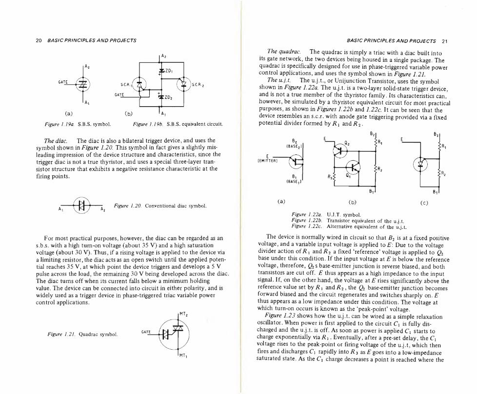
The s.b.s. The s.b.s., or Silicon Bilateral Switch, uses thè symbol shown in Figure LI9a. The device consists of two identical s.u.s. struc- tures connected in inverse parallel within a single housing, as indicated by thè equivalent Circuit of Figure 1.19b. The device acts as a voltage-
triggered switch that can be fired by either polarity of voltage.
20 BASIC PRfNCIPL.es AND PROJBCTS
Figure 1.19a. S.B.S. Symbol. Figure LI9b. S.B.S. equivalent Circuit.
The diac. The diac is also a bilateral trigger device, and uses thè symbol shown in Figure 1.20. This Symbol in fact gives a slightly mis- leading impression of thè device structure and characteristics, since thè trigger diac is not a true thyristor, and uses a special three-layer tran¬ sistor structure that exhibits a negative resistance characteristic at thè
fìring points.
Figure 1.20. Conventional diac symbol.
For most practical purposes, however, thè diac can be regarded as an s.b.s. with a high turn-on voltage (about 35 V) and a high saturation voltage (about 30 V). Thus, if a rising voltage is applied to thè device via alimiting resistor, thè diacactsas an open switch until thè applied poten- tial reaches 35 V, at which point thè device triggers and develops a 5 V pulse across thè load, thè remaining 30 V being developed across thè diac,
The diac tums off when its current falls below a minimum holding value. The device can be connected into circuit in either polarity, and is widely used as a trigger device in phase-triggered triac variable power control applications.
MT,
Figure 1.21. Quadrac symbol. GATE
BASIC PR/NC/PL BS AND PROJBCTS 21
The quadrac. The quadrac is simply a triac with a diac built into its gate network, thè two devices being housed in a single package. The quadrac is specifìcally designed for use in phase-triggered variable power control applications, and uses thè symbol shown in Figure 1.21.
The u.j. t. The u.j.t., or Unijunction Transistor, uses thè symbol shown in Figure 1.22a. The u.j.t. is a two-layer solid-state trigger device, and is not a true member of thè thyristor family. Its characteristics can, however, be simulated by a thyristor equivalent circuit for most practical purposes, as shown in Figures L22b and 1.22c. It can be seen that thè device resembles an s.c.r. with anode gate triggering provided via a fixed potential divider formed by R: and/?2.
Fìptre 1.22a. U.J.T. symbol. Figure 1.22b. Transistor equivalent of thè u.j.t. Figure L22c. Alternative equivalent of thè u.j.t.
The device is normally wired in circuit so that B2 is at a fixed positive voltage, and a variable input voltage is applied to E: Due to thè voltage divider action off? ) and R2 a fixed ‘reference’ voltage is applied to Q2
base under this condition. If thè input voltage at E is below thè reference voltage, therefore, Qa s base-emitter junction is reverse biased, and both transistore are cut off. E thus appears as a high impedance to thè input
signal. If, on thè other hand, thè voltage at E rises significanti above thè reference value set by R i and R2, thè Q2 base-emitter junction becomes forward biased and thè circuit regenerates and switches sharply on. E thus appears as a low impedance under this condition. The voltage at which turn-on occurs is known as thè ‘peak-point’ voltage.
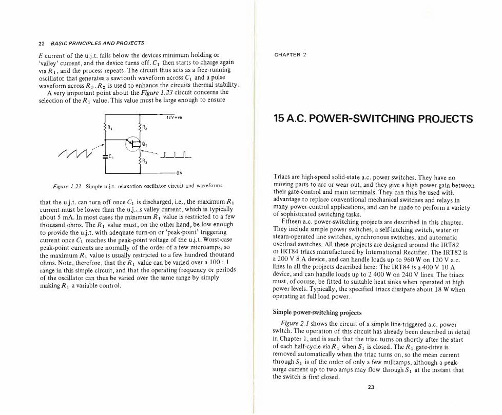
Figure 1.23 shows how thè u.j.t. can be wired as a simple relaxation oscillator. When power is first applied to thè circuit Ci is fully dis- charged and thè u.j.t. is off. As soon as power is applied C\ starts to charge exponentially viaf?i. Eventually, after a pre-set delay, thè Ci voltage rises to thè peak-point or fìring voltage of thè u.j.t, which then
fires and discharges Ci rapidly into R3 as E goes into a low-impedance saturated state. As thè Ci charge decreases a point is reached where thè
22 BASIC PR/NC/PLES AND PROJECTS
E current of thè u.j.t. falls below thè devices minimum holding or ‘valley’ current, and thè device turns off. Cx then starts to charge again viaRi, and thè process repeats. The Circuit thus acts as a free-running
oscillator that generates a sawtooth waveform across Cx and a pulse waveform across R 3. R2 is used to enhance thè circuits thermal stability.
A very important point about thè Figure L23 Circuit concerns thè
selection of thè R i value. This value must be large enough to ensure
/m i :c,
12V+ve
(li
>R3
-ov
Figure 1.23. Simple u.j.t. relaxation oscillator Circuit and waveforms.
that thè u.j.t. can turn off once C\ is discharged, i.e., thè maximum R\ current must be lower thaii thè u.j.t.s valley current, which is typically about 5 mA. In most cases thè mimmumi?i value is restricted to a few
thousand ohms. The Ri value must, on thè other hand, be low enough
to provide thè u.j.t. with adequate turn-on or ‘peak-point’ triggering current once C\ reaches thè peak-point voltage of thè u.j.t. Worst-case peak-point currents are normally of thè order of a few microamps, so
thè maximum Ri value is usually restricted to a few hundred thousand ohms. Note, therefore, that thè Ri value can be varied over a 100 : 1 range in this simple Circuit, and that thè operating frequency or periods
of thè oscillator can thus be varied over thè same range by simply makingRi a variable control.
CHAPTER 2
15A.C. POWER-SWITCHING PROJECTS
Triacs are high-speed solid-state a.c. power switches. They have no
moving parts to are or wear out, and they give a high power gain between their gate-control and main terminals. They can thus be used with advantage to replace conventional mechanical switches and relays in many power-control applications, and can be made to perform a variety of sophisticated switching tasks.
Fifteen a.c. power-switching projeets are described in this chapter.
They include simple power switches, a self-latching switch, water or steam-operated line switches, synchronous switches, and automatic overload switches. All these projeets are designed around thè IRT82 or IRT84 triacs manufactured by International Rectifler. The IRT82 is a 200 V 8 A device, and can handle loads up to 960 W on 120 V a.c. lines in all thè projeets described here: The IRT84 is a 400 V 10 A device, and can handle loads up to 2 400 W on 240 V lines. The triacs must, of course, be fitted to suitable heat sinks when operated at high power levels. Typically, thè specified triacs dissipate about 18 W when operating at full load power.
Simple power-switching projeets
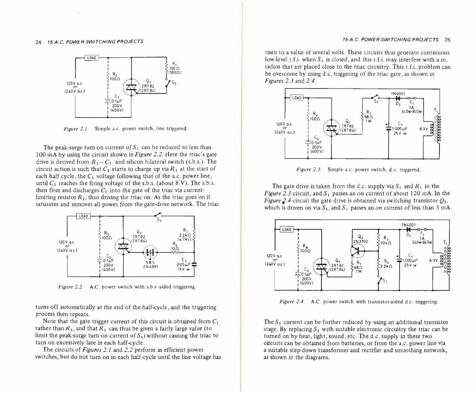
Figure 2A shows thè Circuit of a simple line-triggered a.c. power switch. The operation of this Circuit has already been described in detail
in Chapter 1, and is such that thè triac tums on shortly after thè start of each half-cycle viaRt when Si is closed. The Ri gate-drive is
removed automatically when thè triac turns on, so thè mean current
through S\ is of thè order of only a few milliamps, although a peak- surge current up to two amps may flow through Si at thè instant that thè switch is fìrst closed.
23
24 15 A.C. POWER-SWITCHING PROJECTS
Figure 2.L Simple a.c. power switch, line triggered.
The peak-surge tum-on current ofSi can be reduced to less than 100 mA by using thè Circuit shown in Figure 2.2. Here thè triac’s gate
drive isderived from R\-C\ and Silicon bilateral switch(s.b.s.). The Circuit action is such that C\ starts to charge up via^i at thè start of each half cycle, thè C\ voltage following that of thè a.c. power line, until C\ reaches thè fìring voltage of thè s.b.s. (about 8 V). The s.b.s. then fires and discharges Ci into thè gate of thè triac via current- limiting resistor R2, thus driving thè triac on. As thè triac goes on it saturates and removes all power from thè gate-drive network. The triac
Figure 2.2. A.C. power switch with s.b.s-aided triggering.
tums off automatically at thè end of thè half<yeie, and thè triggering process then repeats.
Note that thè gate trigger current of this Circuit is obtained from Ci rather than^i, and that^i can thus be given a fairly large value (to limit thè peak-surge tum-on current of Si) without causing thè triac to turn on excessively late in each halfxycle.
The circuits of Figures 2.1 and 2.2 perform as efficient power
switches, but do not turn on in each half-cycle until thè line voltage has
15 A.C. POWER-SWITCHING PROJECTS 25
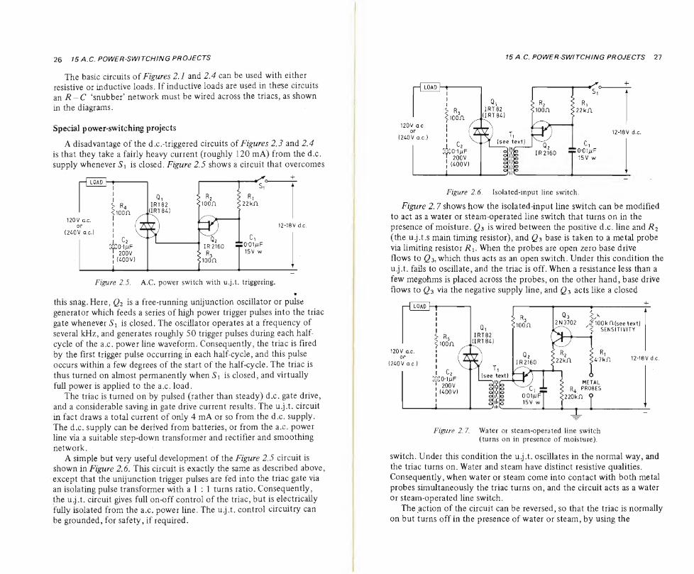
risen to a value of several volts. These circuits thus generate continuous low-level r.f.i. when Si is closed, and this r.f.i. may interfere with a.m. radios that are placed dose to thè triac circuitry. This r.f.i. problem can be overcome by using d.c. triggering of thè triac gate, as shown in Figures 2.3 and 2.4.
Figure 2.3. Simple a.c. power switch, d.c. triggered.
The gate drive is taken from thè d.c. supply via Si and Ri in thè Figure 2.3 Circuit, and Si passes an on current of about 120 mA. In thè
Figure2>A Circuit thè gate drive is obtained via switching transistor Q2, which is driven on via Si, and Si passes an on current of less than 3 mA.
Figure 2.4. A.C. power switch with transistor-aided d.c. triggering.
The Si current can be further reduced by using an additional transistor stage. By replacingS! with suitable electronic circuitry thè triac can be tumed on by heat, light, sound, etc. The d.c. supply in these two circuits can be obtained from batteries, or from thè a.c. power line via a suitable step-down transformer and rectifìer and smoothing network, as shown in thè diagrams.
MW
26 15 A.C. POWER-SWITCHING PROJECTS
The basic circuits of Figures 2.1 and 2.4 can be used with either resistive or inductive loads. If inductive loads are used in these circuits an R-C ‘snubber’ network must be wired across thè triacs, as shown
in thè diagrams.
Special power-switching projects
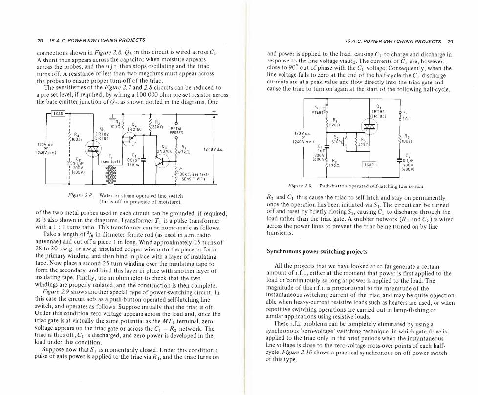
A disadvantage of thè d.c.-triggered circuits of Figures 23 and 2.4 is that they take a fairly heavy current (roughly 120 mA) from thè d.c. supply whenever *Si is closed. Figure 2.5 shows a circuit that overcomes
this snag.Here, Q2 is a free-running unijunction oscillator or pulse
generator which feeds a series of high power trigger pulses into thè triac
gate whenever Si is closed. The oscillator operates at a frequency of several kHz, and generates roughly 50 trigger pulses during each half- cycle of thè a.c. power line waveform. Consequently, thè triac is fìred by thè fìrst trigger pulse occurring in each half-cycle, and this pulse occurs within a few degrees of thè start of thè half-cycle. The triac is thus turned on almost permanently when Si is closed, and virtually
full power is applied to thè ax. load. The triac is turned on by pulsed (rather than steady) dx. gate drive,
and a considerable saving in gate drive current results. The u.j.t. circuit in fact draws a total current of only 4 mA or so from thè dx. supply. The dx. supply can be derived from batteries, or from thè ax. power line via a suitable step-down transformer and rectifier and smoothing network.
A simple but very useful development of thè Figure 2.5 circuit is shown in Figure 2.6. This circuit is exactly thè same as described above, except that thè unijunction trigger pulses are fed into thè triac gate via an isolating pulse transformer with a 1 : 1 turns ratio. Consequently, thè u.j.t. circuit gives full on-off control of thè triac, but is electrically fully isolated from thè ax. power line. The u.j.t. control circuitry can
be grounded, for safety, if required.
15 A.C. POWER-SWITCHING PROJECTS 27
Figure 2.6. Isolated-input line switch.
Figure 2.7 shows how thè isolated-input line switch can be modified to act as a water or steam-operated line switch that turns on in thè presence of moisture. Q3 is wired between thè positive dx. line and R2 (thè u.j.t.s main timing resistor), and Q3 base is taken to a metal probe via limiting resistor Ri. When thè probes are open zero base drive flows to Q3, which thus acts as an open switch. Under this condition thè
u.j.t. fails to oscillate, and thè triac is off. When a resistance less than a
few megohms is placed across thè probes, on thè other hand, base drive flows to Q3 via thè negative supply line, and Q3 acts like a closed
Figure 2. 7. Water or steam-operated line switch (turns on in presence of moisture).
switch. Under this condition thè u.j.t. oscillates in thè normal way, and thè triac turns on. Water and steam have distinct resistive qualities. Consequently, when water or steam come into contact with both metal probes simultaneously thè triac turns on, and thè circuit acts as a water or steam-operated line switch.
The action of thè circuit can be reversed, so that thè triac is normally on but turns off in thè presence of water or steam, by using thè
28 15A.C. POWER-SWITCHING PROJECTS
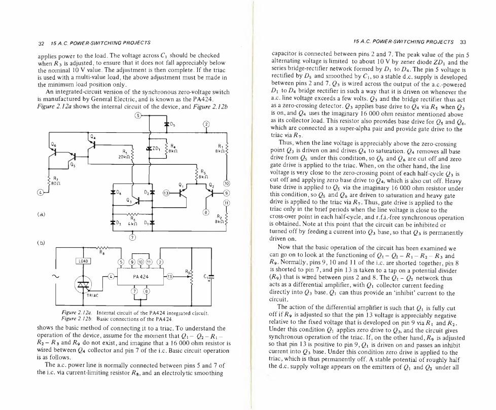
connections shown in Figure 2.8. Q3 in this Circuit is wired across Cv. A shunt thus appears across thè capacitor when moisture appears across thè probes, and thè u.j.t. then stops oscillating and thè triac turns off. A resistance of less than two megohms must appear across thè probes to ensure proper turn-off of thè triac.
The sensitivities of thè Figure 2. 7 and 2.8 circuits can be reduced to a pre-set level, if required, by wiring a 100 000 ohm pre-set resistor across thè base-emitter junction of as shown dotted in thè diagrams. One
Figure 2.8. Water or steam-operated line switch (turns off in presence of moisture).
of thè two metal probes used in each Circuit can be grounded, if required, as is also shown in thè diagrams. Transformer 7\ is a pulse transformer with a 1 : 1 turns ratio. This transformer can be home-made as follows.
Take a length of 3/8 in diameter ferrite rod (as used in a.m. radio antennae) and cut off a piece 1 in long. Wind approximately 25 turns of 28 to 30 s.w.g. or a.w.g. insulated copper wire onto thè piece to form
thè primary winding, and then bind in place with a layer of insulating tape. Now place a second 25-turn winding over thè insulating tape to form thè secondary, and bind this layer in place with another layer of insulating tape. Finally, use an ohmmeter to check that thè two
windings are properly isolated, and thè construction is then complete. Figure 2.9 shows another special type of power-switching Circuit. In
this case thè Circuit acts as a push-button operated self-latching line switch, and operates as follows. Suppose initially that thè triac is off.
Under this condition zero voltage appears across thè load and, sin ce thè triac gate is at virtually thè same potential as thè MTi terminal, zero
voltage appears on thè triac gate or across thè Ci - R2 network. The triac is thus off, Ci is discharged, and zero power is developed in thè load under this condition.
Suppose now that Si is momentarily closed. Under this condition a pulse of gate power is applied to thè triac via Rls and thè triac turns on
1SA.C. POWER-SWITCHING PROJECTS 29
and power is applied to thè load, causing C\ to charge and discharge in response to thè line voltage via R2. The currents of Ci are, however, dose to 90° out of phase with thè Ci voltage. Consequently, when thè line voltage falls to zero at thè end of thè half-cycle thè Ci discharge currents are at a peak value and flow directly into thè triac gate and cause thè triac to turn on again at thè start of thè following half-cycle.
Figure 2.9. Push-button operated self-latching line switch.
^2 and Ci thus cause thè triac to self-latch and stay on permanently once thè operation has been initiated via Si. The Circuit can be turned
off and reset by briefly closingS2, causing Ci to discharge through thè load rather than thè triac gate. A snubber network (R4 and C2 ) is wired across thè power lines to prevent thè triac being turned on by line transients.
Synchronous power-switching projects
All thè projects that we have looked at so far generate a certain amount of r.f.i., either at thè moment that power is first applied to thè
load or continuously so long as power is applied to thè load. The
magnitude of this r.f.i. is proportional to thè magnitude of thè
instantaneous switching current of thè triac, and may be quite objection- able when heavy-current resistive loads such as heaters are used, or when repetitive switching operations are carried out in lamp-flashing or similar applications using resistive loads.
These r.f.i. problems can be completely eliminated by using a synchronous ‘zero-voltage’ switching technique, in which gate drive is applied to thè triac only in thè brief periods when thè instantaneous line voltage is dose to thè zero-voltage cross-over points of each half- cycle. Figure 2.10 shows a practical synchronous on-off power switch of this type.

30 15 A.C. POWER-SWITCHING PROJECTS
Basically, thè Circuit contains a line-driven 'zero-crossing’ detector section and a d.c.-powered triac-gate-drive section. These two sections are interconnected in such a way that a brief pulse of gate current is applied to thè triac only when thè line voltage is dose to zero in each half-cycle. £2 and £3 form thè zero-crossing detector, and are driven from thè a.c. power line by current-limiting potential divider R2- R 3. The Q2 - £3 connection is such that one or other of these transistor is
R,
Figure 2.10. Zero-switching synchronous line switch (turns on with Si closed).
driven on whenever thè line voltage exceeds a certain ‘reference’ value (adjustable down to 4*2 V via ^3), irrespective of thè line voltage polarity, and so that both transistor turn off when thè line voltage is below this reference value. The coilectors of Q2 and £3 are coupled to
thè base of £4 via R4, and £4 uses R$ as its collector load when Si is closed. also provides base drive to £s. £s uses R6 and thè triac gate
as its collector load. £4 and £s are powered from a zener-regulated d.c. supply derived from thè a.c. supply line via R1 - Di - ZD\ and C\.
To understand thè Circuit action, assume that Si is closed and that thè instantaneous a.c. line voltage is at some value in excess of thè reference value of, say, 5 V. Under this condition either £2 or £3 is driven on and drives £4 to saturation via/?4. £4 has a saturation voltage that is lower than thè base-emitter turn-on voltage of £s, so zero base drive flows to £s under this condition, and £s is cut off and zero gate
drive is applied to thè triac. Suppose now that thè instantaneous line voltage falls below thè 5 V
reference value, i.e., that thè line voltage is very near thè zero-voltage
15 A.C. POWER-SWITCtflNG PROJECTS 31
cross-over point near thè end of one half-cycle and thè start of thè next. Under this condition £2 and £3 both turn off and remove thè base drive of £4, which also turns off. Since Q4 is cut off, heavy base drive flows to £s via Rs, and £s is driven to saturation. Heavy gate current thus flows into thè triac gate via £s and R6 from thè 10 V d.c. supply under this condition, and this current turns thè triac on and causes it to self-latch for thè dura tion of thè half-cycle. Thus, gate trigger current is applied to thè triac only in thè brief periods when thè line voltage is dose to zero at thè beginning and end of each half cycle, and negligible r.f.i. is generated under these switching conditions.
Note from thè above description of Circuit opera tion that gate drive can be applied to thè triac only when base drive is available to £s via R5. The triac can thus be turned off or ‘inhibited’ by removing this base drive. The base drive can be removed in a number of ways. In
Figure 2.10 it is removed by wiring on-off switch Si in series with Rs, so thè triac in this Circuit turns on only when Si is closed. In Figure 2.11, on thè other hand, it is removed by driving £4 permanently on
via R4, and in this case thè triac turns on only when Si is open.
Ri
The width of thè gate pulse of thè synchronous switching circuits
can be varied via R3. The width must be adjusted to ensure that thè pulse does not end until thè triac main-terminal currents havè risen above thè holding current in each half-cycle, otherwise thè triac will fail to self-latch. To adjust/^3, connect thè selected power load in place, set/^3 to maximum resistance, and apply power to thè unit. Now reduce thè ^3 value just past thè point at which thè triac turns on and
32 15 A.C. POWER-SWITCHfNG PROJECTS
applies power to thè load. The voltage across Cv should be checked when/? 3 is adjusted, to ensure that it does not fall appreciably below thè nominai 10 V value. The adjustment is then complete. If thè triac is used with a multi-value load, thè above adjustment must be made in thè minimum load position only.
An integrated-circuit version of thè synchronous zero-voltage switch is manufactured by General Electric, and is known as thè PA424. Figure 2J2a shows thè internai Circuit of thè device, and Figure 2.12b
Figure 2.12a. Internai Circuit of thè PA424 integrateci Circuit. Figure 2.12b. Basic connections of thè PA424.
shows thè basic method of connecting it to a triac. To understand thè
operation of thè device, assume for thè moment that Qi - Q2~ R\- R2- Rs and R9 do not exist, and imagine that a 16 000 ohm resistor is wired between Q4 collector and pin 7 of thè i.c. Basic Circuit operation is as follows.
The a.c. power line is normally connected between pins 5 and 7 of thè ix. via current-limiting resistor /?8, and an electrolytic smoothing
15 A.C. POWER-SWITCHING PROJECTS 33
capacitor is connected between pins 2 and 7. The peak value of thè pin 5 alternating voltage is limited to about 10 V by zener diode ZDX and thè series bridge-rectifìer network formed by Dx to D4. The pin 5 voltage is rectifìed by Ds and smoothed by Cu so a stable dx. supply is developed between pins 2 and 7. Q3 is wired across thè output of thè a.c.-powered
Di to bridge rectifìer in such a way that it is driven on whenever thè ax. line voltage exceeds a few volts. Q3 and thè bridge rectifìer thus act as a zero-crossing detector. Q3 applies base drive to Q4 via Rs when Q3 is on, and Q4 uses thè imaginary 16 000 ohm resistor mentioned above as its collector load. This resistor also provides base drive for Qs and Q6, which are connected as a super-alpha pair and provide gate drive to thè triac via/?7.
Thus, when thè line voltage is appreciably above thè zero-crossing point Q3 is driven on and drives Q4 to saturation. Q4 removes all base drive from Qs under this condition, so Qs and Q6 are cut off and zero gate drive is applied to thè triac. When, on thè other hand, thè line
voltage is very dose to thè zero-crossing point of each half-cycle Q3 is cut off and applying zero base drive to Q4, which is also cut off. Heavy base drive is applied to Qs via thè imaginary 16 000 ohm resistor under this condition, so Qs and Q6 are driven to saturation and heavy gate drive is applied to thè triac via /?7. Thus, gate drive is applied to thè triac only in thè brief periods when thè line voltage is dose to thè
cross-over point in each half-cycle, and r.fìi.-free synchronous operation is obtained. Note at this point that thè Circuit can be inhibited or
turned off by feeding a current into Q3 base, so that Q3 is permanently driven on.
Now that thè basic operation of thè Circuit has been examined we can go on to look at thè functioning of Qx - Q2 - RY - R2 - R3 and R9. Normally, pins 9, 10 and 11 of thè ix. are shorted together, pin 8
is shorted to pin 7, and pin 13 is taken to a tap on a potential divider (R9) that is wired between pins 2 and 8. The Qx - Q2 network thus acts as a differential amplifìer, with Qx collector current feeding
directly into Q3 base. Qx can thus provide an ‘inhibit’ current to thè Circuit.
The action of thè differential amplifìer is such that Qx is fully cut off if R9 is adjusted so that thè pin 13 voltage is appreciably negative relative to thè fìxed voltage that is developed on pin 9 via/?! andR2. Under this condition Qi applies zero drive to Q3ì and thè Circuit gives synchronous operation of thè triac. If, on thè other hand,/?9 is adjusted so that pin 13 is positive to pin 9,QX is driven on and passes an inhibit current into Q3 base. Under this condition zero drive is applied to thè triac, which*is thus permanently off. A stable potential of roughly half thè d.c. supply voltage appears on thè emitters of Qx and Q2 under all
34 15 A.C- POWER-SW/TCH/NG PROJECTS
conditions. In thè PA424, therefore,i?3 is wired between this point and thè collector of Qa, and serves both as a ‘tail’ for thè differential amplifier and as a collector load resistor for Qa (in place of thè imaginary 16 000 ohms resistor mentioned earlier).
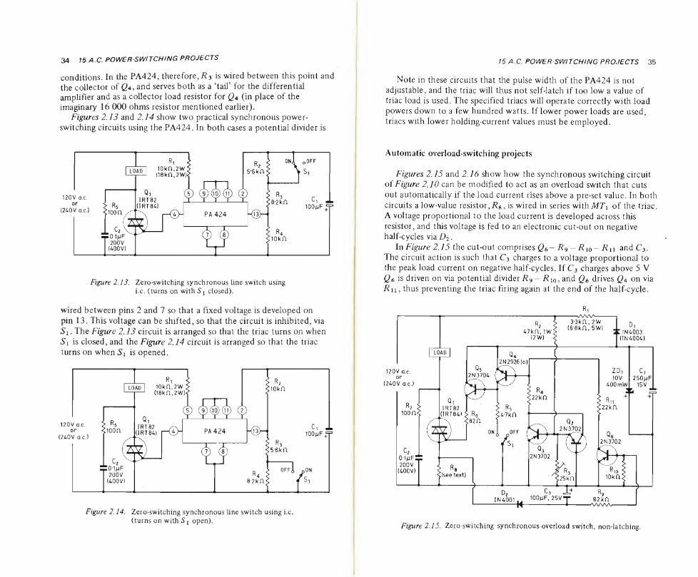
Figures 2.13 and 2.14 show two practical synchronous power- switching circuits using thè PA424. In both cases a potential divider is
Figure 2.13. Zero-switching synchronous line switch using i.c. (turns on with S\ closed).
wired between pins 2 and 7 so that a fixed voltage is developed on
pin 13. This voltage can be shifted, so that thè Circuit is inhibited, via Si. The Figure 2.13 Circuit is arranged so that thè triac turns on when
is closed, and thè Figure 2.14 Circuit is arranged so that thè triac turns on when Si is opened.
Figure 2.14. Zero-switching synchronous line switch using i.c. (turns on with Sl open).
15 A.C. POWER-SWITCHING PROJECTS 35
Note in these circuits that thè pulse width of thè PA424 is not adjustable, and thè triac will thus not self-latch if too low a value of triac load is used. The specified triacs will operate correctly with load powers down to a few hundred watts. If lower power loads are used, triacs with lower holding-current values must be employed.
Automatic overload-switching projects
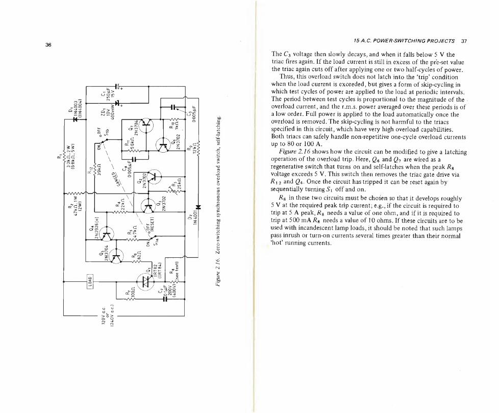
Figures 2.15 and 2.16 show how thè synchronous switching Circuit of Figure 2.10 can be modifìed to act as an overload switch that cuts
out automatically if thè load current rises above a pre-set value. In both circuits a low-value resistor,^, is wired in series withMTX of thè triac. A voltage proportional to thè load current is developed across this resistor, and this voltage is fed to an electronic cut-out on negative half-cycles via Z)2.
In Figure 2.15 thè cut-out comprises Qe~ R9 - R\o- R\\ and C3. The Circuit action is such that C3 charges to a voltage proportional to thè peak load current on negative half-cycles. If C3 charges above 5 V Q6 is driven on via potential divider R9 - Rl0, and Q6 drives Qa on via R11, thus preventing thè triac firing again at thè end of thè half-cycle.
Ri
Figure 2.15. Zero-switching synchronous overload switch, non-latching.
Fig
ure
2.1
6.
Zer
o-s
wit
chin
g s
yn
chro
no
us
ov
erlo
ad s
wit
ch,
self
-lat
chin
g.
15 A.C. POWER-SWITCHING PROJECTS 37
The C3 voltage then slowly decays, and when it falls below 5 V thè triac fires again. If thè load current is stili in excess of thè pre-set value thè triac again cuts off after applying one or two half-cycles of power.
Thus, this overload switch does not latch into thè ‘trip’ condition when thè load current is exceeded, but gives a form of skip-cycling in which test cycles of power are applied to thè load at periodic intervals. The period between test cycles is proportional to thè magnitude of thè - overload current, and thè r.m.s. power averaged over these periods is of a low order. Full power is applied to thè load automatically once thè overload is removed. The skip-cycling is not harmful to thè triacs specified in this circuit, which have very high overload capabilities.
Both triacs can safely handle non-repetitive one-cycle overload currents up to 80 or 100 A.
Figure 2.16 shows how thè circuit can be modifled to give a latching operation of thè overload trip. Here, Q6 and Qn are wired as a regenerative switch that turns on and self-latches when thè peak/?g voltage exceeds 5 V. This switch then removes thè triac gate drive via Rii and Qa. Once thè circuit hastripped it can be reset again by sequentially turningiS'i off and on.
R% in these two circuits must be chosen so that it develops roughly 5 V at thè required peak trip current; e.g., if thè circuit is required to trip at 5 A peak, R8 needs a value of one ohm, and if it is required to trip at 500 mA Rs needs a value of 10 ohms. If these circuits are to be
used with incandescent lamp loads, it should be noted that such lamps
pass inrush or turn-on currents several times greater than their normal ‘hot’ running currents.
CHAPTER 3
20 ELECTRONIC ALARM PROJECTS
The high power gains, low leakage currents, and high current carrying
capacities of s.c.r .s make them ideal for use in a variety of electronic alarm projects. A range of such projects are described in this chapter, and include both simple and advanced burglar alarms, light-beam alarms, smoke alarms, automa tic fìre alarms, over-temperature alarms, frost
alarms, under-temperature alarms, and alarm circuits that are operated by contact with water or steam.
All of these projects are designed around thè IR106Y1 s.c.r. manufactured by International Rectifier, and are reasonably versatile circuits. The alarm that each Circuit uses can be any self-interrupting bell, buzzer, or siren that draws an operating Circuit of less than 2 A. Each Circuit must be operated from a battery supply roughly 1 *5 V greater than thè nominai operating voltage of thè alarm device used.
When building these projects, check that thè s.c.r. does not get too hot when thè alarm is driven on. If it does, connect thè s.c.r. heat tab to a heat sink with an area of a couple of square inches or greater.
Contact-operated alarm projects
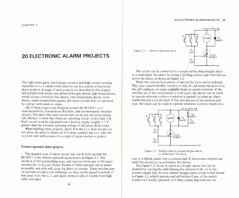
The simplest type of alarm Circuit that can be built around thè IR106Y1 is thè remote-operated alarm shown in Figure 5.7. The
Circuit is of thè non-latching type, and operates when any of thè input switches (Si to Sy) are closed. Dozens of these switches can be wired in parallel, and each will cause thè alarm to operate. These switches pass on currents of only a few milliamps, so they can be placed hundreds of feet away from thè s.c.r. and alarm, without risk of trouble from high cable resistance.
38
20 ELECTRONIC ALARM PROJECTS 39
Figure 3.1. Remote-operated alarm.
4-5 to 13-5V +ve
The Circuit can be converted to a simple self-latching burglar alarm or a multi-input fìre alarm by wiring a latching resistor and reset button across thè alarm, as shown in Figure 3.2.
These two circuits have plenty of uses in thè home and in industry.
They pass typical standby currents of only OT juA when thè alarm is in thè off condition, so cause negligible drain on supply batteries. If thè
switches are of thè microswitch or reed types, thè alarms can be made to operate whenever a door or window is opened, or when an object
travels beyond a pre-set limit. If thè switches are of thè pressure-pad type, thè alarm can be made to operate whenever a person stands on a
4'5 to 13-5V +ve
Figure 3.2. Simple make-to-operate burglar alarm, or multi-input fire alarm.
mat or a vehicle passes over a pressure-pad. If thermostat switches are used, thè circuits act as automatic fìre alarms.
The Figure 3.2. Circuit is useful as a burglar alarm, but can be disabled by cutting thè cable linking thè switches to R\ or to thè positive supply line. A more reliable burglar alarm Circuit is that shown
in Figure 3.3, which operates and self-latches if any of thè switch contacts are briefly operated, or if their connecting leads are cut.

40 20 ELECTRONIC ALARM PROJECTS
C\ is a noise-suppressing capacitar, and ensures that thè aiarm will not be inadvertently operated by thè action of switch contacts momentarily bouncing or sliding apart under vibration or shock conditions; thè aiarm will only operate if thè contacts are held open
for a period in excess of one millisecond or so. The aiarm Circuit of Figure 3.3 draws a standby current of 500 \xA
(via^i) when used with a 6 V supply. The standby current can be
4-5 to 13-5V +ve
Figure 3.3. Break-to-operate burglar aiarm. The Circuit draws a standby current of 500 (J.A at 6 V.
reduced, if required, by increasing thè value of Ri and using a one or two-transistor amplifìer to increase thè gate sensitivity of thè s.c.r., as
shown in Figures 3.4 and 3.5. The Figure 3.4 Circuit draws a standby
current of 60 \iA when operated from a 6 V supply, and thè Figure 3.5 Circuit draws a standby current of 1 *4 }iA under thè same condition.
4-5 to 13-5V+ve
Figure 3.4. Break-to-operate burglar aiarm, drawing a standby current of 60 fJiA at 6 V.
20 ELECTRONIC ALARM PROJECTS 41
The break-to-operate burglar aiarms of Figures 3.3 to 3.5 are far more useful than thè simple-make-to-operate type of Figure 3.2, but are stili not fully tamper proof. They can be disabled by connecting a
jumper lead across thè normally closed switch contacts. This snag can be overcome by combining both break-to-operate and make-to-operate
4*5 to 13*5V +ve
Figure 3.5. Break-to-operate burglar aiarm, drawing a standby current of 1 -4 fJiA at 6 V.
switches in a single aiarm, as shown in thè circuits of Figures 3.6 and
3.7. A burglar is unlikely to know which aiarm leads are of thè break or
make types, and if he cuts or shorts thè wrong ones thè aiarm will instantly sound and self-latch.
The Figure 3.6 tamper-proof aiarm is developed by combining thè circuits of Figures 3.2 and 3.3, and draws a standby current of 500 jiA
4*5 to 13-5V +ve
Figure 3.6. Simple ‘tamper-proof’ burglar aiarm, drawing a standby current of 500 J1A at 6 V.
42 20 ELECTRONIC ALARM PROJECTS
from a 6 V supply. The Figure 3.7 Circuit is developed by combining thè circuits of Figures 3.2 and 3.5; and draws a standby current of 1 *4 juA from a 6 V supply.
All thè burglar alarm circuits looked at so far turn on and self-latch as soon as any of thè input switches are operated. Consequently, if thè owner turns thè alarm on to standby from within a protected building
4-5 io 13-5V +ve
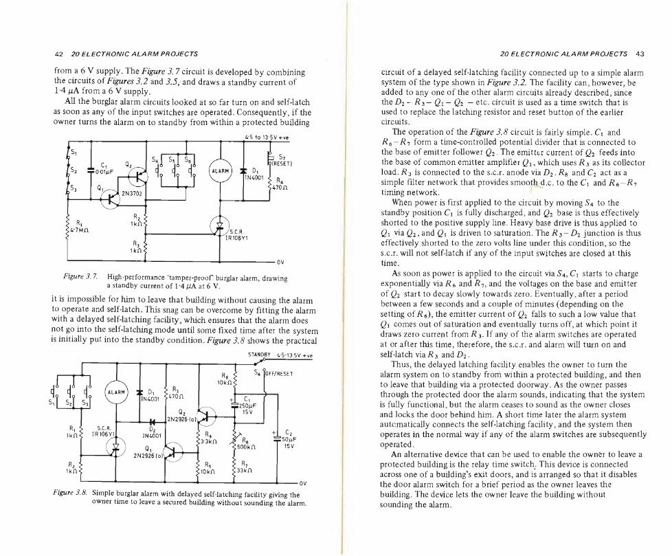
Figure 3.7. High-performance ‘tamper-proof1 burglar alarm, drawing a standby current of 1-4 flA at 6 V.
it is impossible for him to leave that building without causing thè alarm to operate and self-latch. This snag can be overcome by fìtting thè alarm with a delayed self-latching facility, which ensures that thè alarm does not go into thè self-latching mode until some fìxed time after thè System is initiaUy put into thè standby condition. Figure 3.8 shows thè practìcal
STANDBY 45-13-5V +ve
20 ELECTRONIC ALARM PROJECTS 43
Circuit of a delayed self-latching facility connected up to a simple alarm System of thè type shown in Figure 3.2. The facility can, however, be added to any one of thè other alarm circuits already described, since thè £)2 - R$ - Qi - Q2 — etc. Circuit is used as a time switch that is used to replace thè latching resistor and reset button of thè earlier circuits.
The operation of thè Figure 3.8 Circuit is fairly simple. Ci and R6-Ri form a time-controlled potential divider that is connected to
thè base of emitter follower Q2. The emitter current of Q2 feeds into thè base of common emitter amplifier Q\, which uses R* as its collector load. R3 is connected to thè s.c.r. anode via D2. R$ and C2 act as a simple filter network that provides smooth d.c. to thè C\ and R6—Rn timing network.
When power is first applied to thè circuit by moving Sa to thè standby position Ci is fully discharged, and Q2 base is thus effectively shorted to thè positive supply line. Heavy base drive is thus applied to Q1 via Q2> and Q\ is driven to saturation. The R$-D2 junction is thus
effectively shorted to thè zero volts line under this condition, so thè s.c.r. will not self-latch if any of thè input switches are closed at this time.
As soon as power is applied to thè circuit via Sa, C\ starts to charge
exponentially via R& and Rn, and thè voltages on thè base and emitter
of Q2 start to decay slowly towards zero. Eventually, after a period between a few seconds and a couple of minutes (depending on thè setting of R6), thè emitter current of Q2 falls to such a low value that Qi Comes out of saturation and eventually turns off, at which point it draws zero current from R3. If any of thè alarm switches are operated
at or after this time, therefore, thè s.c.r. and alarm will turn on and self-latch via R2 and D2.
Thus, thè delayed latching facility enables thè owner to turn thè alarm System on to standby from within a protected building, and then to leave that building via a protected doorway. As thè owner passes through thè protected door thè alarm sounds, indicating that thè System is fully functional, but thè alarm ceases to sound as thè owner closes and locks thè door behind him. A short time later thè alarm System autcmatically connects thè self-latching facility, and thè System then operates in thè normal way if any of thè alarm switches are subsequently operated.
An alternative device that can be used to enable thè owner to leave a protected building is thè relay time switch. This device is connected across one of a building’s exit doors, and is arranged so that it disables thè door alarm switch for a brief period as thè owner leaves thè building. The device lets thè owner leave thè building without sounding thè alarm.
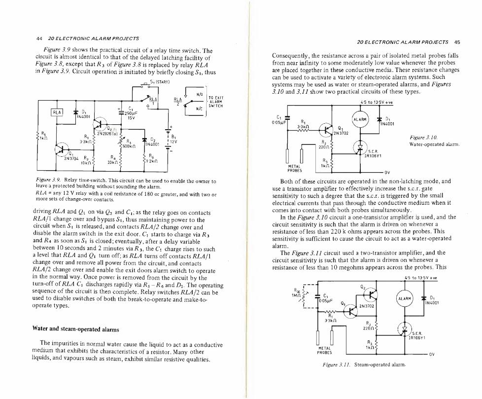
44 20 ELECTRONIC ALARM PROJECTS
Figure 3.9 shows thè practical Circuit of a relay time switch. The Circuit is almost identical to that of thè delayed latching facility of Figure 3.8, except that R3 of Figure 3.8 is replaced by relay RLA in Figure 3.9. Circuit operation is initiated by briefly closing Si, thus
Figure 3.9. Relay time-switch. This Circuit can be used to enable thè owner to leave a protected building without sounding thè alami.
RLA = any 12 V relay with a coil resistance of 180 or gieater, and with two or more sets of change-over contacts.
drivingRL^l and Q\ on via Q2 and C\\ as thè relay goes on contacts
RLA/1 change over and bypass Si, thus maintaining power to thè Circuit when Si is released, and contacts RLA/2 change over and
disable thè alarm switch in thè exit door. Ci starts to charge via R3 and R4 as soon as Si is closed; eventually, after a delay variable
between 10 seconds and 2 minutes via ^3, thè Ci charge rises to such a level that RLA and Qi turn off; as RLA turns off contacts RLA/1 change over and remove all power from thè Circuit, and contacts
RLA/2 change over and enable thè exit doors alarm switch to operate in thè normal way. Once power is removed from thè Circuit by thè turn-off of RLA Ci discharges rapidly via Rs-R6 and j02. The operating sequence of thè Circuit is then complete. Relay switches RLA/2 can be used to disable switches of both thè break-to-operate and make-to- operate types.
Water and steam-operated alarms
The impurities in normal water cause thè liquid to act as a conductive medium that exhibits thè characteristics of a resistor. Many other liquids, and vapours such as steam, exhibit similar resistive qualities.
20 ELECTRONIC ALARM PROJECTS 45
Consequently, thè resistance across a pair of isolated metal probes falls from near infinity to some moderately low value whenever thè probes are placed together in these conductive media. These resistance changes can be used to activate a variety of electronic alarm systems. Such systems may be used as water or steam-operated alarms, and Figures 3.10 and 3.11 show two practical circuits of these types.
4-5 to 13-5V +ve
Figure 3.10.
Water-operated alarm.
Both of these circuits are operated in thè non-latching mode, and use a transistor amplifier to effectively increase thè s.c.r. gate sensitivity to such a degree that thè s.c.r. is triggered by thè small electrical currents that pass through thè conductive medium when it Comes into contact with both probes simultaneously.
In thè Figure 3.10 Circuit a one-transistor amplifier is used, and thè Circuit sensitivity is such that thè alarm is driven on whenever a resistance of less than 220 k ohms appears across thè probes. This sensitivity is sufflcient to cause thè Circuit to act as a water-operated
alarm. The Figure 3.11 circuit used a two-transistor amplifier, and thè
Circuit sensitivity is such that thè alarm is driven on whenever a resistance of less than 10 megohms appears across thè probes. This
4-5 io 13-5V + ve
Figure 3.11. Steam-operated alaim.
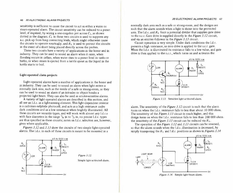
46 20 ELECTRONIC ALARM PROJECTS
sensitivity is suffìcient to cause thè Circuit to act as either a water or steam-operated alarm. The Circuit sensitivity can be reduced to a preset level, if required, by wiring a one-megohm pot across C\, as shown dotted in thè diagram. C\ in these two circuits is used to suppress any a.c. pick-up from long connecting leads, which might otherwise cause thè circuits to operate erratically, andR\ is used to protect thè circuits in thè event of a short being placed directly across thè probes.
These two circuits have a variety of applications in thè home and in industry. They can be used to sound an alarm when it rains, when
flooding occurs in cellars, when water rises to a preset level in tanks or baths, or when steam is ejected from a kettle spout as thè liquid in thè kettle starts to boil.
Light-operated alarm projects
Light-operated alarms have a number of applications in thè home and in industry. They can be used to sound an alarm when light enters a normally dark area, such as thè inside of a safe or strong-room, or they can be used to sound an alarm if an intruder or object breaks a projected light beam. They can also be used as smoke-sensitive alarms.
A variety of light-operated alarms are described in this section, and all use an l.d.r. as a light-sensing element. This light-dependent resistor
is a cadmium-sulphide photocell, and acts as a high resistance under dark conditions and as a low resistance when brightly illuminated. All these circuits are versatile types, and will work with almost any l.d.r.s
with face diameters in thè range Vs ?n10 V2 in; no precise l.d.r. types are thus specifìed in these circuits; notes on l.d.r. selection are, however, given where applicable.
Figures 3.12 and 3.13 show thè circuits of two simple light-operated alarms. The l.d.r. in each of these circuits is meant to be mounted in a
4-5 to 13-5V + ve
Figure 3.12.
Simple light-activated alarm.
20 ELECTRONIC ALARM PROJECTS 47
normally dark area such as a safe or strong-room, and thè designs are such that thè alarm sounds when a light is shone into thè protected area. The l.d.r. and R1 form a potential divider that supplies gate drive to thè s.c.r. Gate drive is supplied directly in thè Figure 3.12 Circuit,
and via an emitter-follower in thè Figure 3.13 Circuit. Circuit operation is very simple. Under dark conditions thè l.d.r.
presents a high resistance, so zero drive is applied to thè s.c.r. gate. When thè l.d.r. is illuminated its resistance falls to a low value, and gate drive is then applied to thè s.c.r., which turns on and activates thè
4-5 to 13-5V +ve
Figure 3.13. Sensitive light-activated alarm.
alarm. The sensitivity of thè Figure 3.12 Circuit is such that thè alarm turns on when thè l.d.r. resistance falls to less than about 10 000 ohms. The sensitivity of thè Figure 3.13 Circuit is much higher, and this design turns on when thè l.d.r. resistance falls to less than 200 000 ohms. thè sensitivity of thè Figure 3.13 Circuit can be reduced via R1.
The operation of thè Figure 3.12 and 3.13 circuits can be reversed, so that thè alarm sounds when thè l.d.r. illumination is decreased, by simply transposing thè R\ and l.d.r. positions as shown in Figures 3.14
4-5 to 13'5V +ve

48 20 ELECTRONIC ALARM PROJECTS
and 3.15. These two circuits can be used as simple interrupted-light-beam alarms. Normally, thè l.d.r. rs brightly illuminateci via a projected light- beam and lens System. The l.d.r. presents a low resistance under this condition, and zero drive is applied to thè gate of thè s.c.r., which is thus off. When a person or object enters thè light beam thè l.d.r.
4-5 to 13-5V + ve
Figure 3.15. Alternative light-beam alarm.
resistance rises to a high value, and gate drive is then applied to thè s.c.r., which turns on and sounds thè alarm.
The l.d.r. in thè Figure 3.14 Circuit can be any type that offers a resistance less than 1 000 ohms under thè illuminated condition, and more than 3 000 ohms under thè ‘interrupted’ condition. The Figure
3.15 circuit can be used with any l.d.r. that offers a resistance less than about 50 000 ohms under thè illuminated condition.
The circuits of Figures 3.14 and 3.15 act as useful intrusion alarms in many applications, but are not suitable for use as high-security
burglar alarms. Both circuits can be disabled by shining a bright light, with an intensity greater than that of thè normal light-beam, on to thè l.d.r. face. This vulnerability of thè basic light-beam alarm can be
overcome in a number of ways. Figure 3.16 shows one circuit that overcomes thè problem.
Here, thè l.d.r. is wired in a bridge network formed by Rx - R2- Ri-R* and thè l.d.r., and Qx and Q2 are wired as bridge balance
detectors that apply gate drive to thè s.c.r. The circuit action is such that thè bridge is balanced and thè alarm is off when thè l.d.r. is
illuminated normally by thè light beam, and is such that thè bridge goes out of balance and thè alarm goes on if thè l.d.r. illumination varies from thè normal level by even a small amount. The alarm thus goes on if thè light-beam is interrupted or if a bright light is shone on thè l.d.r. face, and thè circuit acts as an ‘unbeatable’ light-beam alarm.
To understand thè circuit operation, assume thè following points. The circuit is powered from a 10 V supply.Rx is adjusted so its
20 ELECTRONIC ALARM PROJECTS 49
resistance is equal to that of thè l.d.r. in thè normal ‘balanced’ condition in which thè l.d.r. is illuminated by thè light-beam, so 5 V is developed on Qi base and Q2 emitter under this condition. R$ is adjusted so that 5*6 V is developed on Qi emitter, and 44 V is developed on Q2 base, i.e., a forward bias of 600 mV is developed
LIGHT BEAM 4*5 to 13-5V+ve
between thè base-emitter junctions of Q1 and Q2 under thè normal balanced condition. Q\ and Q2 each turn on when thè forward base-emitter bias rises to 650 mV.
Thus, under thè normal balanced condition a forward bias is applied to both Qi and Q2, but is not sufficient to cause either transistor to conduct, so thè s.c.r. and alarm are off. Suppose, however, that thè light-beam is interrupted, so that thè l.d.r. resistance increases. Under
this condition thè voltage at thèLDR—Ri junction falls appreciably below 5 V, so thè Qi forward base-emitter bias rises above 650 mV, and Qi conducts and drives on thè s.c.r. and thè alarm.
Alternatively, suppose that a bright light, with an intensity greater than that of thè basic light-beam, is shone on thè l.d.r. face, so that thè l.d.r. resistance decreases. In this case thè voltage at thè LDR-Ri junction rises appreciably above 5 V, so thè Q2 forward base-emitter bias rises above 650 mV, and Q2 conducts and again drives on thè s.c.r. and thè alarm.
The circuit thus operates thè alarm if thè l.d.r. illumination varies from thè normal light-beam level by an amount sufficient to cause a
voltage change greater than50 mV at thè LDR-R\ junction. The sensitivity of thè circuit can be varied via R3i and can be set to such high levels that thè alarm can be activated by changes in light level too small to be detected by thè human eye.
The l.d.r. used in thè Figure 3.16 circuit can be any type giving a resistance in thè range 200 ohms to 2 000 ohms when illuminated by
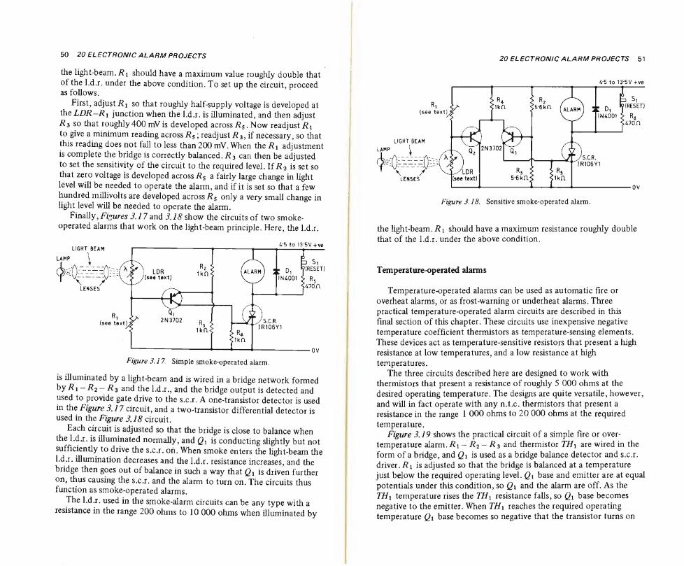
50 20 ELECTRONIC ALARM PROJECTS
thè light-beam.should have a maximum value roughly doublé that °f thè l.d.r. under thè above condition. To set up thè Circuit, proceed as follows.
First, adjust/?i so that roughly half-supply voltage is developed at thè LDR—Rx junction when thè l.d.r. is illuminated, and then adjust Rs so that roughly400 mVis developed across R$. Now readjust Ri to give a minimum reading across R$ ; readjust R3, if necessary, so that this reading does not fall to less than 200 mV. When thè Ri adjustment is complete thè bridge is correctly balanced. R3 can then be adjusted to set thè sensitivity of thè Circuit to thè required level. If R$ is set so
that zero voltage is developed across R$ a fairly large change in light level will be needed to operate thè alami, and if it is set so that a few
hundred millivolts are developed across R$ only a very small change in light level will be needed to operate thè alarm.
Finally,Figures 3.17and 3.18 show thè circuits of two smoke- operated alarms that work on thè light-beam principle. Here, thè l.d.r.
4'5 to 13'5V +ve
is illuminated by a light-beam and is wired in a bridge network formed byRx-R2 — Rz and thè l.d.r., and thè bridge output is detected and used to prò vide gate drive to thè s.c.r. A one-transistor detector is used in thè Figure 3A7 Circuit, and a two-transistor differential detector is used in thè Figure 3A8 Circuit.
Each circuit is adjusted so that thè bridge is dose to balance when thè l.d.r. is illuminated normally, and Q\ is conducting slightly but not suffìciently to drive thè s.c.r. on. When smoke enters thè light-beam thè
l.d.r. illumination decreases and thè l.d.r. resistance increases, and thè bridge then goes out of balance in such a way that Qx is driven further on, thus causing thè s.c.r. and thè alarm to turn on. The circuits thus function as smoke-operated alarms.
The l.d.r. used in thè smoke-alarm circuits can be any type with a resistance in thè range 200 ohms to 10 000 ohms when illuminated by
20 ELECTRONIC ALARM PROJECTS 51
4-5 to 13-5V +ve
thè light-beam. R\ should have a maximum resistance roughly doublé that of thè l.d.r. under thè above condition.
Temperature-operated alarms
Tempera ture-opera ted alarms can be used as automatic fìre or
overheat alarms, or as frost-warning or underheat alarms. Three
practical temperature-operated alarm circuits are described in this fìnal section of this chapter. These circuits use inexpensive negative temperature coefficient thermistors as temperature-sensing elements.
These devices act as temperature-sensitive resistors that present a high resistance at low temperatures, and a low resistance at high
temperatures. The three circuits described here are designed to work with
thermistors that present a resistance of roughly 5 000 ohms at thè desired operating temperature. The designs are quite versatile, however, and will in fact operate with any n.t.c. thermistors that present a resistance in thè range 1 000 ohms to 20 000 ohms at thè required
temperature. Figure 3A9 shows thè practical Circuit of a simple fìre or over-
temperature alarm.R\- R2 — R$ and thermistor TH\ are wired in thè form of a bridge, and Q\ is used as a bridge balance detector and s.c.r.
driver.R% is adjusted so that thè bridge is balanced at a temperature just below thè required operating level. Q\ base and emitter are at equal potentials under this condition, so Q% and thè alarm are off. As thè
TH% temperature rises thè TH1 resistance falls, so Q\ base becomes negative to thè emitter. When TH\ reaches thè required operating temperature Q\ base becomes so negative that thè transistor turns on
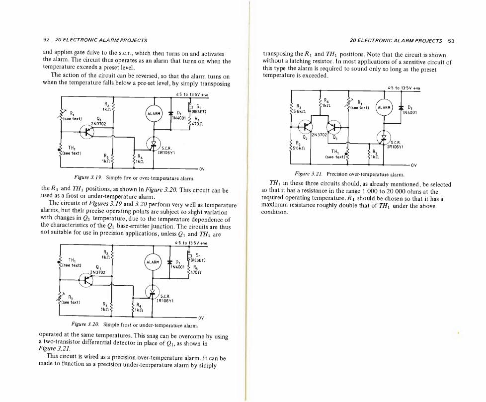
52 20 ELECTRONIC ALARM PROJECTS
and applies gate drive to thè s.c.r., which then turns on and activates thè alarm. The Circuit thus operates as an alarm that turns on when thè temperature exceeds a preset level.
The action of thè Circuit can be reversed, so that thè alarm turns on when thè temperature falls below a pre-set level, by simply transposing
4-5 to 13’5V +ve
Figure 3.19. Simple Tire or over-temperature alarm.
thè Ri and THX positions, as shown in Figure 3.20. This Circuit can be used as a frost or under-temperature alarm.
The circuits of Figures 3.19 and 3.20 perform very well as temperature alarms, but their precise operating points are subject to slight variation
with changes in Q\ temperature, due to thè temperature dependence of
thè characteristics of thè Qx base-emitter junction. The circuits are thus not suitable for use in precision applications, unless Qx and THX are
4'5 to 13*5V +ve
Figure 3.20. Simple frost or under-temperature alarm.
operateci at thè same temperatures. This snag can be overcome by using a two-transistor differential detector in place of Q\, as shown in Figure 3.21.
This Circuit is wired as a precision over-temperature alarm. It can be made to function as a precision under-temperature alarm by simply
20 ELECTRONIC ALARM PROJECTS 53
transposing thè Ai and Tti\ positions. Nòte that thè Circuit is shown without a latching resistor. In most applications of a sensitive Circuit of this type thè alarm is required to sound only so long as thè preset temperature is exceeded.
Figure 3.21. Precision over-temperature alarm.
THi in these three circuits should, as already mentioned, be selected so that it has a resistance in thè range 1 000 to 20 000 ohms at thè required operating temperature. A i should be chosen so that it has a maximum resistance roughly doublé that of TH\ under thè above condition.
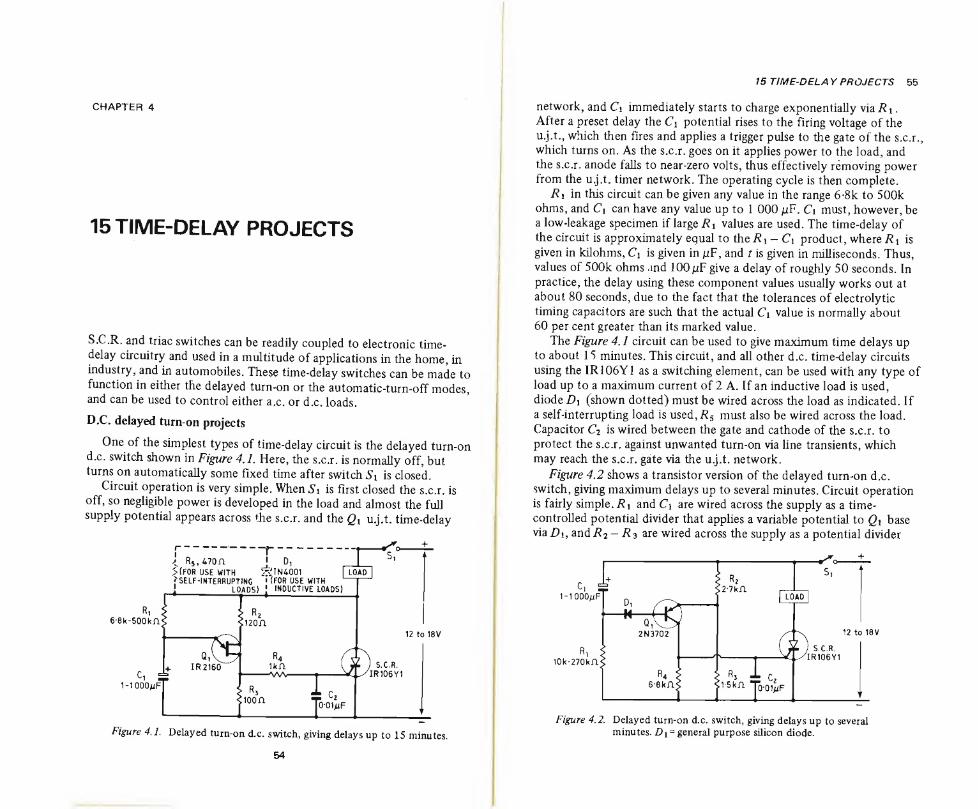
CHAPTER 4
15 TIME-DELAY PROJECTS
S.C.R. and triac switches can be readily coupled to electronic time-
delay circuitry and used in a multitude of applications in thè home, in
industry, and in automobiles. These time-delay switches can be made to function in either thè delayed turn-on or thè automatic-turn-off modes, and can be used to control either a.c. or d.c. loads.
D.C. delayed turn-on projects
One of thè simplest types of time-delay Circuit is thè delayed turn-on d.c. switch shown in Figure 4.1. Here, thè s.c.r. is normally off, but turns on automatically some fixed time after switch Si is closed.
Circuit operation is very simple. When Si is fìrst closed thè s.c.r. is off, so negligale power is developed in thè load and almost thè full supply potential appears across thè s.c.r. and thè Qy u.j.t. time-delay
Figure 4.1. Delayed turn-on d.c. switch, giving delays up to 15 minutes.
54
15 TiME-DELA Y PROJECTS 55
network, and C\ immediately starts to charge exponentially via Ry. After a preset delay thè Cy potential rises to thè fìring voltage of thè u.j.t., which then fìres and applies a trigger pulse to thè gate of thè s.c.r., which turns on. As thè s.c.r. goes on it applies power to thè load, and thè s.c.r. anode falls to near-zero volts, thus effectively rémoving power from thè u.j.t. timer network. The operating cycle is then complete.
Ri in this Circuit can be given any value in thè range 6*8k to 500k ohms, and Ci can have any value up to 1 000 iiF. Ci must, however, be a low-leakage specimen if large Ri values are used. The time-delay of
thè Circuit is approximately equal to thè Ri - Ci product, whereRi is given in kilohms, Ci is given in jLtF, and t is given in milliseconds. Thus, values of 500k ohms and ÌOOjjF give a delay of roughly 50 seconds. In practice, thè delay using these component values usually works out at about 80 seconds, due to thè fact that thè tolerances of electrolytic timing capacitors are such that thè actual Ci value is normally about 60 per cent greater than its marked value.
The Figure 4.1 Circuit can be used to give maximum time delays up to about 15 minutes. This Circuit, and all other d.c. time-delay circuìts
using thè IR106Y1 as a switching element, can be used with any type of load up to a maximum current of 2 A. If an inductive load is used, diode Di (shown dotted) must be wired across thè load as indicated. If a self-interrupting load is used, Rs must also be wired across thè load.
Capacitor C2 is wired between thè gate and cathode of thè s.c.r. to protect thè s.c.r. against unwanted turn-on via line transients, which may reach thè s.c.r. gate via thè u.j.t. network.
Figure 4.2 shows a transistor version of thè delayed turn-on d.c. switch, giving maximum delays up to several minutes. Circuit operation is fairly simple.Ri and Ci are wired across thè supply as a time- controlled potential divider that applies a variable potential to Qi base viaZ)i, andR2- R3 are wired across thè supply as a potential divider
Figure 4.2. Delayed turn-on d.c. switch, giving delays up to several minutes. Z>i = generai purpose Silicon diode.
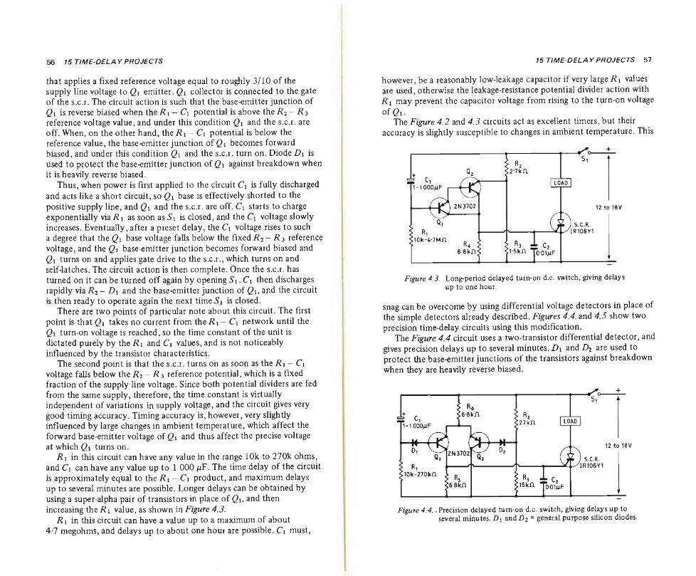
56 15 TIME-DELA Y PROJECTS
that applies a fìxed reference voltage equal to roughly 3/10 of thè supply line voltage to Q\ emitter. Q\ collector is connected to thè gate of thè s.c.r. The Circuit action is such that thè base-emitter junction of Qi is reverse biased when thè R i - C\ potential is above thè R2- R 3
reference voltage value, and under this condition Qi and thè s.c.r. are off. When, on thè other hand, thè Ri - C1 potential is below thè reference value, thè base-emitter junction of Q\ becomes forward biased, and under this condition Q\ and thè s.c.r. turn on. Diode Di is used to protect thè base-emitter junction of Q\ against breakdown when
it is heavily reverse biased. Thus, when power is first applied to thè Circuit C\ is fully discharged
and acts like a short Circuit, so Q\ base is effectively shorted to thè
positive supply line, and Q\ and thè s.c.r. are off. C\ starts to charge exponentially via R\ as soon as Si is closed, and thè C\ voltage slowly
increases. Eventually, after a preset delay, thè C\ voltage rises to such a degree that thè Q\ base voltage falls below thè fìxed R2- R 3 reference voltage, and thè Q\ base-emitter junction becomes forward biased and
Q\ turns on and applies gate drive to thè s.c.r., which turns on and self-latches. The Circuit action is then complete. Once thè s.c.r. has turned on it can be turned off again by opening Si. C\ then discharges rapidly via R2 - Di and thè base-emitter junction of Qi, and thè Circuit
is then ready to operate again thè next time Si is closed. There are two points of particular note about this Circuit. The first
point is that Qi takes no current from thè Ri - Ci network until thè
Qi turn-on voltage is reached, so thè time Constant of thè unit is dictated purely by thè Ri and Ci values, and is not noticeably
influenced by thè transistor characteristics. The second point is that thè s.c.r. turns on as soon as thè Ri - Ci
voltage falls below thè R2- R 3 reference potential, which is a fìxed fraction of thè supply line voltage. Since both potential dividers are fed from thè same supply, therefore, thè time Constant is virtually independent of variations in supply voltage, and thè Circuit gives very good timing accuracy. Timing accuracy is, however, very slightly influenced by large changes in ambient temperature, which affect thè forward base-emitter voltage of Qi and thus affect thè precise voltage
atwhichQi turns on. Ri in this circuit can ha ve any value in thè range lOk to 270k ohms,
and Ci can have any value up to 1 000 fiF. The time delay of thè circuit
is approximately equal to thè Ri - Ci product, and maximum delays up to several minutes are possible. Longer delays can be obtained by
using a super-alpha pair of transistors in place of Qu and then
increasing thè Ri value, as shown in Figure 4.3. Ri in this circuit can have a value up to a maximum of about
4*7 megohms, and delays up to about one hour are possible. Ci must,
15 TIME-DELA Y PROJECTS 57
however, be a reasonably low-leakage capacitor if very large Ri values are used, otherwise thè leakage-resistance potential divider action with Ri may prevent thè capacitor voltage from rising to thè turn-on voltage
of Qi. The Figure 4.2 and 4.3 circuits act as excellent timers, but their
accuracy is slightly susceptible to changes in ambient temperature. This
Figure 4.3. Long-period delayed turn-on d.c. switch, giving delays up to one hour.
snag can be overcome by using differential voltage detectors in place of thè simple detectors already described. Figures 4.4. and 4.5 show two
precision time-delay circuits using this modification. The Figure 4.4 circuit uses a two-transistor differential detector, and
gives precision delays up to several minutes. Di and D2 are used to protect thè base-emitter junctions of thè transistors against breakdown
when they are heavily reverse biased.
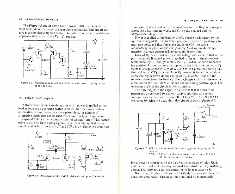
58 15 TIME DELA Y PROJECTS
The Figure 4.5 Circuit uses a four-transistor differential detector, with each side of thè detector super-alpha connected. This Circuit can give precision delays up to one hour. In both circuits thè time-delay is approximately equal to thè Rx - Ci product.
Figure 4.5. Precision long-period delayed turn-on d.c. switch, giving delays up to one hour.
D.C. auto-tum-off projects
Auto-turn-off circuits are designs in which power is applied to thè load as soon as an operating switch is closed, but thè power is then automatically removed again after a preset delay. A number of
alternative techniques can be used to achieve this type of operation. Figure 4.6 shows thè practical Circuit of an auto-turn-off d.c. switch
using two s.c.r.s. In this design power is permanently applied to thè
Circuit, and SCR ì is normally off and SCR2 is on. Under this condition
Figure 4.6. Auto-turn-off d.c. switch, giving delays up to 15 minutes.
15 T/ME-DELA Y PROJECTS 59
zero power is developed across thè load, near-zero voltage is developed across thè u.j.t. timer network, and C2 is fully charged with its SCRi-anode side positive.
Power is applied to thè load by briefly closing push-button switch Si, thus drivingSCRi on. As SCRi goes on its anode drops sharply to near-zero volts, and thus forces thè anode of SCR2 to swing momentarily negative via thè charge of C2. As SCR2 anode swings negative its anode current falls to zero, and it turns off.
Once SCR2 has turned off its anode voltage rises dose to that of thè positive supply line, and power is applied to thè u.j.t. timer network. Simultaneously, C2 charges rapidly via /?3, its SCR2-anode end becom- ing positive. As soon as power is applied to thè u.j.t. timer network Ci starts to charge exponentially via R^9 and after a preset period thè u.j.t. fires and turns SCR2 back on. As SCR2 goes on it forces thè anode of SCRi sharply negative via thè charge of C2, so SCR i turns off and removes power from thè load. C2 then recharges rapidly in thè reverse direction via thè load, its SCRi-anode end becoming positive again. The operating cycle of thè Circuit is then complete.
The only snag with thè Figure 4.6 Circuit is that it needs to be permanently connected to a power supply, and thus consumes a
Constant standby current of about 20 mA (via R 3). This snag can be overcome by using thè s.c.r.-plus-relay circuit shown in Figure 4.7.
Figure 4. 7. SCR relay auto-turn-off d.c. switch, giving delays up to 15 minutes. RLA = 12 V relay with coil resistance in thè range 120 £2 to
1000 12: one set of N/O contacts.
Here, power is connected to thè load via thè contacts of relay RLA, and thè s.c.r. and u.j.t. circuitry are used to control thè relay switching action. The relay has a coil resistance'that is large relative to Ri.
Normally, thè relay is off, so contact RLA fi is open and thè circuit
consumes zero power. Circuit action is initiated by momentarily
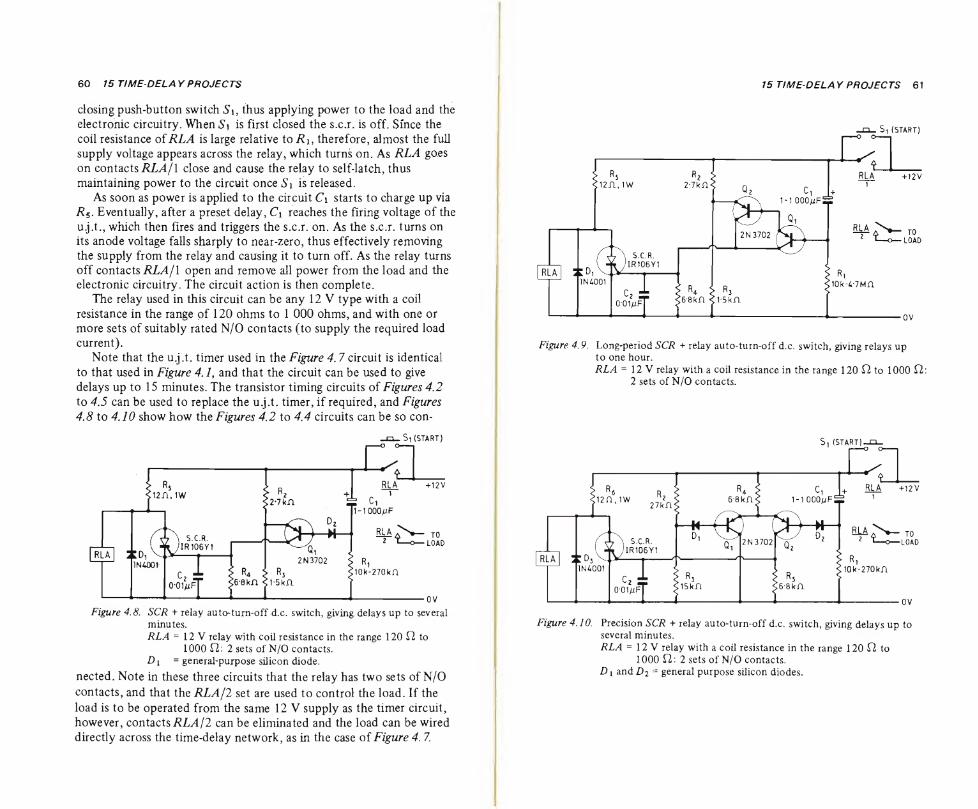
60 15 T/ME-DELA Y PROJECTS
closing push-button switch Si, thus applying power to thè load and thè electronic circuitry. When Si is first closed thè s.c.r. is off. Sfnce thè coil resistance of RLA is large relative io Ri> therefore, almost thè full supply voltage appears across thè relay, which turns on. As RLA goes
on contacts/£/,>!/1 dose and cause thè relay to self-latch, thus maintaining power to thè Circuit once Si is released.
As soon as power is applied to thè Circuit C\ starts to charge up via R5. Eventually, after a preset delay, C\ reaches thè flring voltage of thè u.j.t., which then flres and triggers thè s.c.r. on. As thè s.c.r. turns on its anode voltage falls sharply to near-zero, thus effectively removing thè supply from thè relay and causing it to turn off. As thè relay turns off contacts RLA/Ì open and remove all power from thè load and thè electronic circuitry. The Circuit action is then complete.
The relay used in this Circuit can be any 12 V type with a coil
resistance in thè range of 120 ohms to 1 000 ohms, and with one or more sets of suitably rated N/O contacts (to supply thè required load current).
Note that thè u.j.t. timer used in thè Figure 4.7 Circuit is identical
to that used in Figure 4.7, and that thè Circuit can be used to give
delays up to 15 minutes. The transistor timing circuits of Figures 4.2 to 4.5 can be used to replace thè u.j.t. timer, if required, and Figures 4.8 to 4.10 show how thè Figures 4.2 to 4.4 circuits can be so con-
Si (START)
Figure 4.8. SCR + relay auto-turn-off d.c. switch, giving delays up to several minutes. RLA = 12 V relay with coil resistance in thè range 120 f2 to
1000 f2: 2 sets of N/O contacts. Di = general-purpose Silicon diode.
nected. Note in these three circuits that thè relay has two sets of N/O
contacts, and that thè RLA/2 set are used to control thè load. If thè
load is to be operated from thè same 12 V supply as thè timer Circuit,
however, contacts RLA/2 can be eliminated and thè load can be wired directly across thè time-delay network, as in thè case of Figure 4.7.
15 TIME DELA Y PROJECTS 61
$1 (START)
Figure 4.9. Long-period SCR + relay auto-turn-off d.c. switch, giving relays up to one hour. RLA = 12 V relay with a coil resistance in thè range 120 f2 to 1000 f2:
2 sets of N/O contacts.
Figure 4.10. Precision SCR + relay auto-turn-off d.c. switch, giving delays up to several minutes. RLA = 12 V relay with a coil resistance in thè range 120 f2 to
1000 f2: 2 sets of N/O contacts. Dy and Z)2 = generai purpose Silicon diodes.
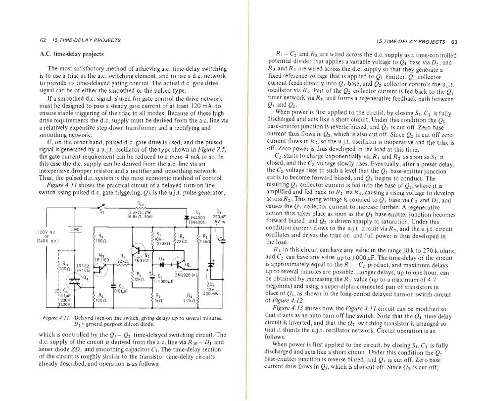
62 15 TiME-DELA Y PROJECTS
A.C. time-delay projects
The most satisfactory method of achieving a.c. time-delay switching is to use a triac as thè a.c. switching element, and to use a d.c. network to provide its time-delayed gating control. The actual d.c. gate drive signal can be of either thè smoothed or thè pulsed type.
If a smoothed d.c. signal is'used for gate control thè drive network must be designed to pass a steady gate current of at least 120 mA, to ensure stable triggering of thè triac in all modes. Because of these high drive requirements thè d.c. supply must be derived from thè a.c. line via a relatively expensive step-down transformer and a rectifying and smoothing network.
If, on thè other hand, pulsed d.c. gate drive is used, and thè pulsed signal is generated by a u.j.t. oscillator of thè type shown in Figure 2.5, thè gate current requirement can be reduced to a mere 4 mA or so. In this case thè d.c. supply can be derived from thè a.c. line via an inexpensive dropper resistor and a rectifìer and smoothing network. Thus, thè pulsed d.c. System is thè most economie method of control.
Figure 4.11 shows thè practical Circuit of a delayed turn-on line switch using pulsed d.c. gate triggering. g3 is thè u.j.t. pulse generator,
Figure 4. IL Delayed turn-on line switch, giving delays up to several minutes. D\ = generai purpose Silicon diode.
which is controlled by thè gì - g2 time-delayed switching Circuit. The d.c. supply of thè Circuit is derived from thè a.c. line viario - Di and zener diode ZDy and smoothing capacitor C\. The time-delay section of thè Circuit is roughly similar to thè transistor time-delay circuits already described, and operation is as follows.
15 TIME-DELA Y PROJECTS 63
Ri - C2 and R2 are wired across thè d.c. supply as a time-controlled potential divider that applies a variable voltage to Qy base via Z)2, and
R3 and R4 are wired across thè d.c. supply so that they generate a fixed reference voltage that is applied to gì emitter. gì collector current feeds directly into Q2 base, and Q2 collector Controls thè u.j.t. oscillator via R2. Part of thè Q2 collector current is fed back to thè Q\ timer network via RSì and forms a regenerative feedback path between gì and g2.
When power is first applied to thè Circuit, by closing Si, C2 is fully discharged and acts like a short Circuit. Under this condition thè gì base-emitter junction is reverse biased, and gì is cut off. Zero base
current thus flows in g2, which is also cut off. Since Q2 is cut off zero
current flows inR2i so thè u.j.t. oscillator is inoperative and thè triac is off. Zero power is thus developed in thè load at this time.
C2 starts to charge exponentially via Ry and/?2 assoonas.S'i is closed, and thè C2 voltage slowly rises. Eventually, after a preset delay, thè C2 voltage rises to such a level that thè gì base-emitter junction starts to become forward biased, and gì begins to conduct. The resulting gì collector current is fed into thè base of g2, where it is amplified and fed back to R2 via Rs, causing a rising voltage to develop across R2. This rising voltage is coupled to gì base via C2 and Z)2, and causes thè gì collector current to increase further. A regenerative action thus takes place as soon as thè gì base-emitter junction becomes forward biased, and g2 is driven sharply to saturation. Under this condition current flows to thè u.j.t. Circuit via Rn, and thè u.j.t. Circuit oscillates and drives thè triac on, and full power is thus developed in thè load.
Ry in this Circuit can have any value in thè range 10 kto 270 k ohms,
and C2 can have any value up to 1 OOOjuF.The time-delay of thè Circuit is approximately equal to thè Ry - C2 product, and maximum delays
up to several minutes are possible. Longer delays, up to one hour, can be obtained by increasing theRy value (up to a maximum of 4*7
megohms) and using a super-alpha connected pair of transistors in
place of gb as shown in thè long-period delayed turn-on switch Circuit of Figure 4.12.
Figure 4.13 shows how thè Figure 4.11 Circuit can be modifìed so that it acts as an auto-turn-off line switch. Note that thè gì time-delay Circuit is inverted, and that thè g2 switching transistor is arranged so that it shunts thè u.j.t. oscillator network. Circuit operation is as follows.
When power is first applied to thè Circuit, by closing Si, Ci is fully discharged and acts like a short Circuit. Under this condition thè gì
base-emitter junction is reverse biased, and gì is cut off. Zero base current thus flows in g2, which is also cut off. Since g2 is cut off,
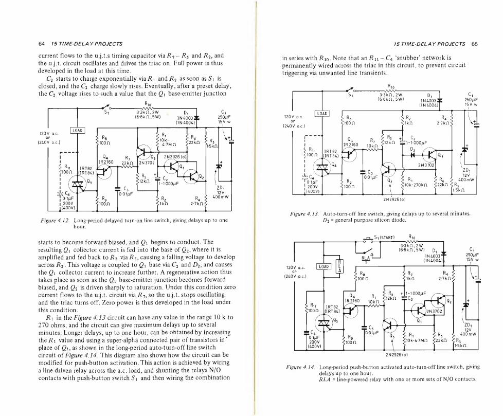
64 15 TIME-DELAY PRO JECTS
current flows to thè u.j.t.s timing capacita- viai?7- R5 and R2t and thè u.j.t. Circuit oscillates and drives thè triac on. Full power is thus developed in thè load at this time.
C2 starts to charge exponentially via Ri and R2 as soon asSi is closed, and thè C2 charge slowly rises. Eventually, after a preset delay, thè C2 voltage rises to such a value that thè Q\ base-emitter junction
Figure 4.12. Long-period delayed turn-on line switch, giving delays up to one hour.
starts to become forward biased, and Q\ begins to conduct. The resulting Q\ collector current is fed into thè base of Q2y where it is amplified and fed back to R2 via R5y causing a falling voltage to develop across R2. This voltage is coupled to Qi base via C2 and D2ì and causes thè Q\ collector current to increase further. A regenerative action thus takes place as soon as thè Q\ base-emitter junction becomes forward biased, and Q2 is driven sharply to saturation. Under this condition zero current flows to thè u.j.t, Circuit via Rn, so thè u.j.t. stops oscillating and thè triac turns off. Zero power is thus developed in thè load under
this condition. R i in thè Figure 4.13 Circuit can have any value in thè range 10 k to
270 ohms, and thè Circuit can give maximum delays up to several
minutes. Longer delays, up to one hour, can be obtainedby increasing thè R\ value and using a super-alpha connected pair of transistors in‘ place of Q\, as shown in thè long-period auto-turn-off line switch Circuit of Figure 4.14. This diagram also shows how thè Circuit can be modifled for push-button activation.This action is achieved by wiring
a line-driven relay across thè a.c. load, and shunting thè relays N/O contacts with push-button switch Si and then wiring thè combination
15 TtME-DELA Y PROJECTS 65
in series with R i0. Note that an R11 - C4 ‘snubber’ network is permanently wired across thè triac in this Circuit, to prevent Circuit
triggering via unwanted line transients.
Figure 4.13. Auto-turn-off line switch, giving delays up to several minutes. D2 = generai purpose Silicon diode.
Figure 4.14. Long-period push-button activated auto-turn-off line switch, giving delays up to one hour. RIA - line-powered relay with one or more sets of N/O contacts.
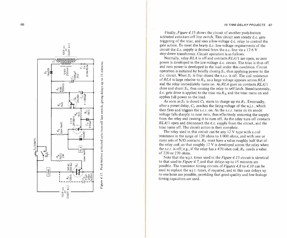
Si
(ST
AR
T)
66
ò <j d o
a 3
O È 3
Ò 3
-i
■l C*.
15 TtME-DELAY PROJECTS 67
Finally, Figure 4.15 shows thè Circuit of another push-button activated auto-turn-off line switch. This Circuit uses steady d.c. gate triggering of thè triac, and uses a low-voltage d.c. relay to control thè gate action. To meet thè heavy d.c. low-voltage requirements of thè Circuit thè d.c. supply is derived from thè a.c. line via a 12*6 V step-down transformer. Circuit operation is as follows.
Normally, relay RLA is off and coniacts RLA/Ì are open, so zero power is developed in thè low-voltage d.c. Circuit. The triac is thus off and zero power is developed in thè load under this condition. Circuit operation is initiated by briefly closingSi, thus applying power to thè d.c. Circuit. When Si is first closed thè s.c.r. is off. The coil resistance of RLA is large relative to R$, so a large voltage appears across RLA and thè relay immediately turns on. As RLA goes on contacts RLA/ì dose and shunt Si, thus causing thè relay to self-latch. Simultaneously, d.c. gate drive is applied to thè triac via R6, and thè triac turns on and applies full power to thè load.
As soon asSi is dosed Ci starts to charge up via/?i. Éventually, after a preset delay, C2 reaches thè firing voltage of thè u.j.t., which then fires and triggers thè s.c.r. on. As thè s.c.r. turns on its anode
voltage falls sharply to near zero, thus effectively removing thè supply from thè relay and causing it to turn off. As thè relay turn off contacts RLA/Ì open and disconnect thè d.c. supply from thè Circuit, and thè triac turns off. The Circuit action is then complete.
The relay used in this Circuit can be any 12 V type with a coil resistance in thè range of 120 ohms to 1 000 ohms, and with one or
more sets of N/O contacts. R5 must have a value roughly half that of* thè relay coil, so that roughly 12 V is developed across thè relay when thè s.c.r. is off; e.g., if thè relay has a 470 ohm coil,/?5 needs a value of 220 or 270 ohms.
Note that thè u.j.t. timer used in thè Figure 4.15 Circuit is identical to that used in Figure 4.7, and that delays up to 15 minutes are possible. The transistor timing circuits of Figures 4.8 to 4.10 can be used to replace thè u.j.t. timer, if required, and in this case delays up to one hour are possible, providing that good-quality and low-leakage timing capacitors are used.
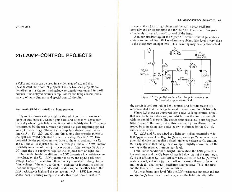
CHAPTER 5
25 LAMP-COIMTROL PROJECTS
S.C.R.s and triacs can be used in a wide range of a.c. and d.c. incandescent lamp control projects. Twenty-fìve such projects are
described in this chapter, and include automatic turn-on and turn-off circuits, time-delayed circuits, lamp flashers and lamp chasers, and a variety of lamp dimmers and special control circuits.
Automatic (light activated) a.c. lamp projects
Figure 5.1 shows a simple light-activated Circuit that turns an a.c.
lamp on automatically when it gets dark, and turns it off again auto¬ ma tically when it gets light. Circuit operation is fairly simple. The lamp is controlled by thè triac, which has pulsed d.c. gate triggering applied via u.j.t. oscillator Q2. The u.j.t.s d.c. supply is derived from thè a.c. line via R5 — Di - ZD\ and Ci, and this supply also provides power to thè light-controlled potential divider formed by Ri and LDR. This potential divider provides emitter drive to thè u.j.t. oscillator viaR2 andZ)2, and Ri is adjusted so that thè voltage at thè Ri -LDR junction is slightly in excess of thè u.j.t.s peak-point or fìring voltage (typically 0*7 times thè d.c. supply voltage) at thè required turn-on light level.
Thus, under bright conditions thè LDR presents a low resistance, so thè voltage on thè Rx - LDR junction is below thè u.j.t.s peak-point voltage. Under this condition, therefore, C2 is unable to charge to thè fìring voltage of thè u.j.t., so thè u.j.t. oscillator is inoperative and thè triac and lamp are off. Under dark conditions, on thè other hand, thè LDR resistance is high and thè voltage on thè R i - LDR junction is above thè u.j.t.s fìring voltage, so under this condition Ci is able to
68
25 LAMP-CONTROL PROJECTS 69
charge to thè u.j.t.s fìring voltage and thè u.j.t. Circuit oscillates normally and drives thè triac and thè lamp on. The Circuit thus gives completely automatic on-off control of thè lamp.
A minor disadvantage of thè Figure 5.1 Circuit is that it generates a certain amount of lamp flicker when thè ambient light level is very dose to thè preset turn-on light level. This flickering may be objectionable if
Figure 5.1. Simple light-activated a.c. lamp, for outdoor use. D2 - generai purpose Silicon diode..
thè Circuit is used for indoor light control, and for this reason it is recommended that thè design be used to control outdoor lights only.
Figure 5.2 shows an improved light-activated lamp control Circuit that is suitable for indoor use, and which turns thè lamp on and off
with no sign of flickering. The Circuit again uses à d.c. pulse-triggered triac to control thè lamp, but in this case thè u.j.t. oscillator is con¬ trolled by a precision light-activated switch formed by thè Q3- Q4 and LDR network.
Ri - LDR and R2 are wired as a light-controlled potential divider that applies a variable voltage to Q4base, and R3-R4 are wired as a potential divider that applies a fixed reference voltage to Q4 emitter. Ri is adjusted so that thè Q4 base voltage is slightly above that of thè emitter at thè required turn-on light level.
Thus, under conditions of bright illumination \heLDR presents a low resistance and thè Q4 base voltage is below that of thè emitter, so Qa is cut off. Since Q4 is cut off zero base current is fed to Q% which is also cut off, and since Q% is cut off zero current flows to thè u.j.t.s emitter viaR7, and thè u.j.t. oscillator is inoperative. Thus, thè triac and thè lamp are off under this condition.
As thè ambient light level falls thè LDR resistance increases and thè voltage on Q4 base rises. Eventually, when thè light intensity falls to
70 25 LAMP-CONTROL PROJECTS
thè preset turn-on level, thè Q4 base voltage rises to such a level that - thè Q4 base-emitter junction becomes forward biased and thè transistor starts to conduct. The resulting collector current of Q4 feeds directly into thè base of where it is amplified, and thè resulting collector
current of Q$ is fed back to Q4 base via Rs - R2 and thè LDR and causes thè 04 base voltage to increase further. Q* thus turns on harder and increases thè drive to Q3) so a regenerative action takes place in which Qz suddenly switches to saturation. Under this condition emitter
current flows to thè u.j.t. via /?7 and Q3, and thè u.j.t. oscillates and
drives thè triac and thè lamp on. Thus, thè triac and thè lamp turn on abruptly when thè light intensity falls to thè preset turn-on level, and thè lamp operates with no sign of flicker. The lamp turns off again when thè LDR illumination rises back above thè preset level, so fully
automatic lamp operation is achieved. The LDR used in thè Figure 5.1 and 5.2 circuits can be any small
cadmium sulphide photocell that offers a resistance in thè range 1 000
Figure 5.2. Improved Iight-activated a.c. lamp, for indoor use.
to 10 000 ohms at thè required turn-on light level. This celi should be mounted at least seven feet above thè ground, so that it is not influenced by shadows thrown by passing people or objects, and should be positioned so that it responds to thè mean light level of thè room or area in which thè controlled lamps are situated. The celi should not be placed in deep shadow or in a position where it is excessively illuminated
by a single point of illumination.
When setting up thè circuits by adjusting/?i, it is important to note that, for satisfactory operation, thè illumination cast on to thè LDR
25 LAMP-CONTROL PROJECTS 11
face by thè lamp must be lower than that cast by thè naturai illumination at thè required preset turn-on level. If this point is not observed a photoelectric positive feedback loop will be created between thè lamp
and thè LDR, and thè Circuit will then function as a lamp flasher or oscillator.
Time-delayed lamp-control projects
All of thè time-delay circuits shown in Chapter 4 can be used to control incandescent lamps, thè final choice of Circuit being a matter o.f individuai preference. Figures 5.3 to 5.6 show thè author’s personal choice of delayed turn-on and auto-turn-off d.c. and a.c. lamp-control circuits.
Figure 5.3 shows a delayed turn-on d.c. lamp Circuit that can give
delays up to 15 minutes. The lamp in this Circuit can be any 12 V type
Figure 5.3. Delayed turn-on d.c. lamp, giving delays up to 15 minutes.
that draws a current less than 2 A. The Circuit is developed from Figure 4.1, and its operation is described in Chapter 4.
Figure 5.4 shows a push-button activated auto-turn-off d.c. lamp Circuit that gives delays up to 15 minutes. The lamp in this Circuit is controlled by relay contacts &L4/1, and thè lamp can thus be any 12 V type with a current rating that can be handled by thè RLA/l contacts.
The relay can be any 12 V type with a coil resistance in thè range 120 to 1 000 ohms, and with one or more sets of suitably rated N/O contacts. The Figure 5.4 Circuit is identical to that of Figure 4.7.
Figure 5.5 shows a delayed turn-on a.c. lamp Circuit that gives delays up to several minutes. Using thè specified triacs thè Circuit can be used to control incandescent lamp loads up to 960 W on 120 V a.c. lines, or
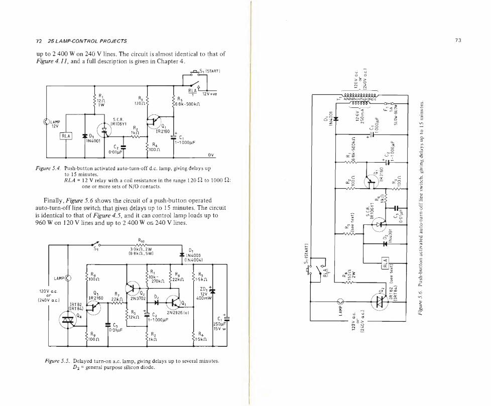
72 25 LAMP-CONTROL PROJECTS
up to 2 400 W on 240 V lines. The Circuit is almost identical to that of Figure 4.11, and a full description is given in Chapter4.
n ^ (START)
Figure 5.4. Push-button activated auto-turn-off d.c. lamp, giving delays up to 15 minutes. RLA = 12 V relay with a coil resistance in thè range 12012 to 1000 12:
one or more sets of N/O contacts.
Finally, Figure 5.6 shows thè Circuit of a push-button operated auto-turn-off line switch that gives delays up to 15 minutes. The Circuit
is identical to that of Figure 4.5, and it can control lamp loads up to 960 W on 120 V lines and up to 2 400 W on 240 V lines.
Figure 5.5. Delayed turn-on a.c. lamp, giving delays up to several minutes. D2 = generai purpose Silicon diode.
Sì
(ST
AR
T)
73
■vQQQQPQQQOQOO
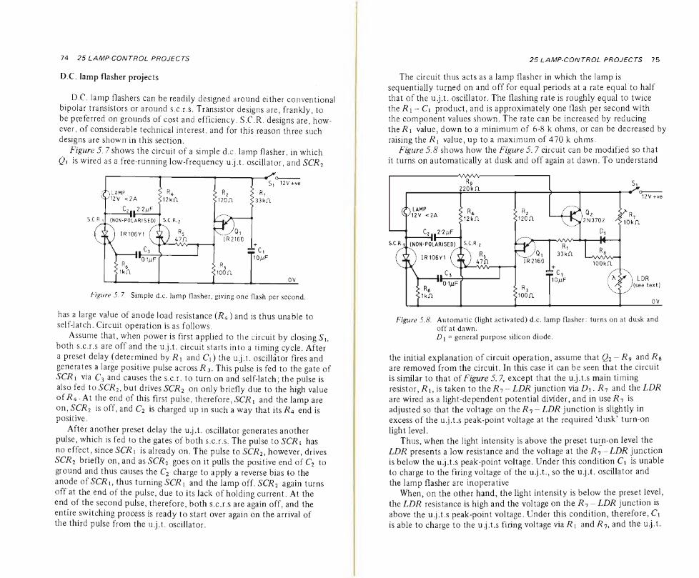
74 25 LAMP-CONTROL PROJECTS
D.C. lamp flasher projects
D.C. lamp flashers can be readily designed around either conventional bipolar transistor or around s.c.r.s. Transistor designs are, frankJy, to be pceferred on grounds of cost and efficiency. S.C.R. designs are, how- ever, of considerable technical interest, and for this reason three such designs are shown in this section.
Figure 5. 7 shows thè Circuit of a simple d.c. lamp flasher, in which
Q) is wired as a free-running low-frequency u.j.t. oscillator, and SCR2
has a large value of anode load resistance (R4) and is thus unable to self-latch. Circuit operation is as follows.
Assume that, when power is first applied to thè circuit by closingSi, both s.c.r.s are off and thè u.j.t. circuit starts into a timing cycle. After a preset delay (determined by Ri and Ci) thè u.j.t. oscillator fires and generates a large positive pulse across /?3. This pulse is fed to thè gate of SCR i via C3 and causes thè s.c.r. to turn on and self-latch; thè pulse is also fed to SCR2ì but drives SCR2 on only briefly due to thè high value of/?4.At thè end of this first pulse, therefore, SCR\ and thè lamp are on, SCR2 is off, and C2 is charged up in such a way that its R$ end is positive.
After another preset delay thè u.j.t. oscillator generates another pulse, which is fed to thè gates of both s.c.r.s. The pulse to SCR 1 has no effect, since SCRi is already on. The pulse to SCR2, however, drives SCR2 briefly on, and as SCR2 goes on it pulls thè positive end of C2 to
ground and thus causes thè C2 charge to apply a reverse bias to thè
anode ofSCRh thus turning SCR 1 and thè lamp off. SCR2 again turns off at thè end of thè pulse, due to its Jack of holding current. At thè
end of thè second pulse, therefore, both s.c.r.s are again off, and thè entire switching process is ready to start over again on thè arrivai of thè third pulse from thè u.j.t. oscillator.
25 LAMP-CONTROL PROJECTS 75
The circuit thus acts as a lamp flasher in which thè lamp is
sequentially turned on and off for equal periods at a rate equal to half that of thè u.j.t. oscillator. The flashing rate is roughly equal to twice thè R \ - Ci product, and is approximately one flash per second with thè component values shown. The rate can be increased by reducing the/?i value, down to a minimum of 6*8 k ohms, or can be decreased by
raising thè R\ value, up to a maximum of 470 k ohms. Figure 5.8 shows how thè Figure 5. 7 circuit can be modified so that
it turns on automatically at dusk and off again at dawn. To understand
Figure 5.8. Automatic (light activated) d.c. lamp flasher: turns on at dusk and off at dawn. D1 = generai purpose Silicon diode.
thè initial explanation of circuit operation, assume that Q2 - R9 and R& are removed from thè circuit. In this case it can be seen that thè circuit is similar to that of Figure 5. 7, except that thè u.j.t.s main timing resistor, Ri, is taken to the/?7 - LDR junction via Di. Ri and thè LDR are wired as a light-dependent potential divider, and in use Ri is adjusted so that thè voltage on th e Ri-LDR junction is slightly in excess of thè u.j.t.s peak-point voltage at thè required ‘dusk’ turn-on
light level. Thus, when thè light intensity is above thè preset turn-on level thè
LDR presents a low resistance and thè voltage at thè Rn-LDR junction is below thè u.j.t.s peak-point voltage. Under this condition Ci is unable to charge to thè firing voltage of thè u.j.t., so thè u.j.t. oscillator and
thè lamp flasher are inoperative When, on thè other hand, thè light intensity is below thè preset level,
thè LDR resistance is high and thè voltage on thè Rn-LDR junction is above thè u.j.t.s peak-point voltage. Under this condition, therefore, Ci is able to charge to thè u.j.t.s firing voltage via/?i and/?7, and thè u.j.t.
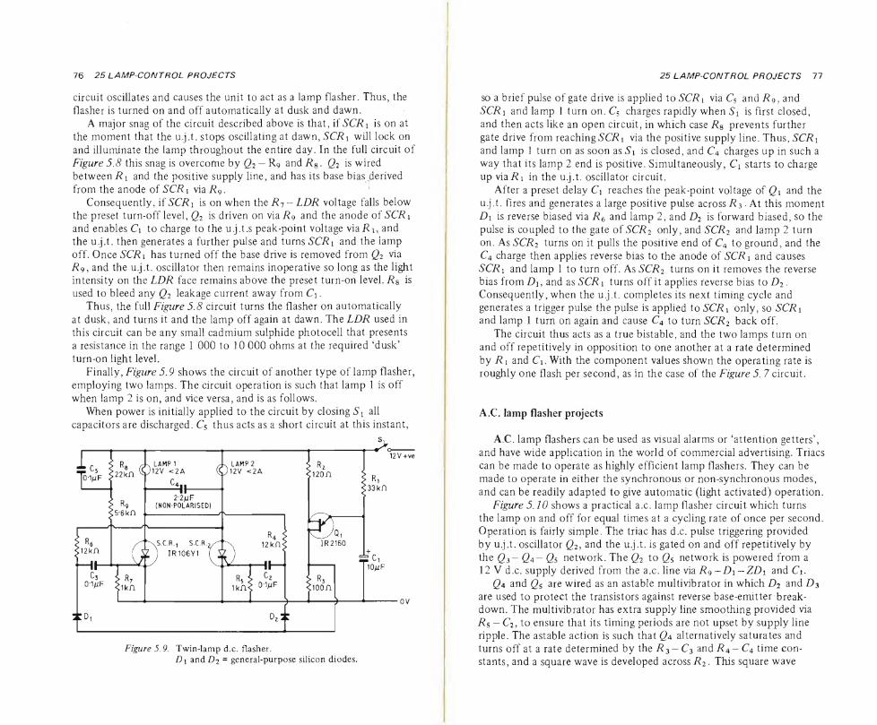
76 25 LAMP-CONTROL PROJECTS
Circuit oscillates and causes thè unit to act as a lamp flasher. Thus, thè flasher is turned on and off automatically at dusk and dawn.
A major snag of thè Circuit described above is that, if SCR i is on at thè moment that thè mj.t. stops oscillating at dawn, SCR 1 will lock on and illuminate thè lamp throughout thè entire day. In thè full Circuit of
Figure 5.8 this snag is overcome by Q2 — R9 and Rg. Q2 is wired betweenRi and thè positive supply line, and has its base bias^derived
from thè anode of SCR 1 via R9. ] Consequently, if SCRi is on when thè R7 - LDR voltage falls below
thè preset turn-off level, Q2 is driven on viaR9 and thè anode of SCR 1
and enables C\ to charge to thè u.j.t.s peak-point voltage via Ri, and thè u.j.t. then generates a further pulse and turns SCR\ and thè lamp off. Once SCR\ has turned off thè base drive is removed from Q2 via R9, and thè u.j.t. oscillator then remains inoperative so long as thè light intensity on thè LDR face remains above thè preset turn-on level. Rg is
used to bleed any Q2 leakage current away from C\. Thus, thè full Figure 5.8 Circuit turns thè flasher on automatically
at dusk, and turns it and thè lamp off again at dawn. The LDR used in this Circuit can be any small cadmium sulphide photocell that presents a resistance in thè range 1 000 to 10 000 ohms at thè required ‘dusk’ turn-on light level.
Finally, Figure 5.9 shows thè Circuit of another type of lamp flasher, employing two lamps. The Circuit operation is such that lamp 1 is off when lamp 2 is on, and vice versa, and is as follows.
When power is initially applied to thè Circuit by closingSj all capacitors are discharged. C5 thus acts as a short circuit at this instant,
Figure 5.9. Twin-lamp d.c. flasher. Dy and £>2 = general-purpose Silicon diodes.
25 LAMP-CONTROL PROJECTS 11
so a brief pulse of gate drive is applied to SCR\ via C5 and R9, and
SCR 1 and lamp 1 turn on. C5 charges rapidly when Si is flrst closed, and then acts like an open circuit, in which case R8 prevents further gate drive from reachingSCRi via thè positive supply line. Thus, SCR 1 and lamp 1 turn on as soon as Si is closed, and C4 charges up in such a way that its lamp 2 end is positive. Simultaneously, Cx starts to charge up via Ri in thè u.j.t, oscillator circuit.
After a preset delay C\ reaches thè peak-point voltage of Q\ and thè u.j.t. fires and generates a large positive pulse across R3. At this moment
Di is reverse biased via R6 and lamp 2, and D2 is forward biased, so thè pulse is coupled to thè gate of SCR2 only, and SCR2 and lamp 2 turn on. As SCR2 turns on it pulls thè positive end of C4 to ground, and thè C4 charge then applies reverse bias to thè anode of SCRi and causes SCRy and lamp 1 to turn off. As SCR2 turns on it removes thè reverse bias from D\, and as SCR 1 turns off it applies reverse bias to D2. Consequently, when thè u.j.t. completes its next timing cycle and generates a trigger pulse thè pulse is applied to SCRi only, so SCRi and lamp 1 turn on again and cause C4 to turn SCR2 back off.
The circuit thus acts as a true bistable, and thè two lamps turn on
and off repetitively in opposition to one another at a rate determined by Ri and Ci. With thè component values shown thè operating rate is roughly one flash per second, as in thè case of thè Figure 5. 7 circuit.
A.C. lamp flasher projects
A.C. lamp flashers can be used as visual alarms or ‘attention getters’, and have wide application in thè world of commercial advertising. Triacs can be made to operate as highly efficient lamp flashers. They can be made to operate in either thè synchronous or non-synchronous modes, and can be readily adapted to give automatic (light activated) operation.
Figure 5.10 shows a practical a.c. lamp flasher circuit which turns thè lamp on and off for equal times at a cycling rate of once per second. Operation is fairly simple. The triac has d.c. pulse triggering provided by u.j.t. oscillator Q2, and thè u.j.t. is gated on and off repetitively by
thè Qs~ Qa~ Qs network. The Q2 to Qs network is powered from a 12 V d.c. supply derived from thè a.c. line via R9-D\ ~ZD\ and C\.
Qa and Qs are wired as an astable multivibrator in which D2 and D3
are used to protect thè transistor against reverse base-emitter break- down. The multivibrator has extra supply line smoothing provided via Rs - C2, to ensure that its timing periods are not upset by supply line ripple. The astable action is such that Qa alternatively saturates and turns off at a rate determined by thè R3- C3 and R4- C4 time con- stants, and a square wave is developed across R2. This square wave
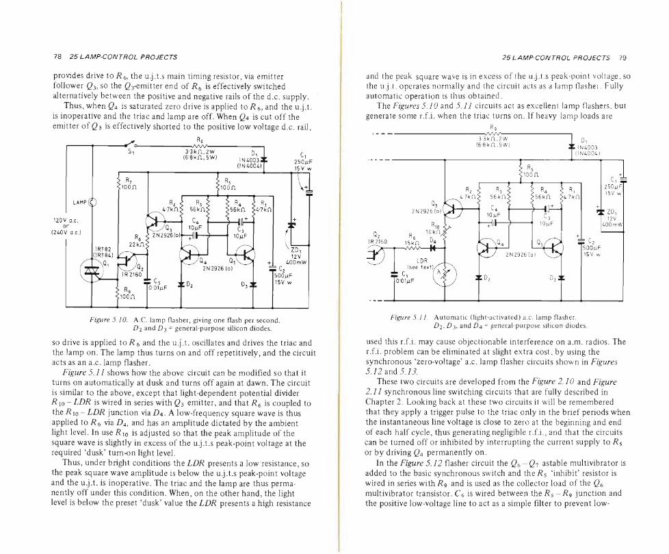
78 25 LAMP-CONTROL PROJECTS
provides drive to R6) thè u.j.t.s main timing resistor, via emitter follower Q3, so thè 23-emitter end of R6 is effectively switched
alternatively between thè positive and negative rails of thè d.c. supply.
Thus, when £4 is saturated zero drive is applied toR6,and theu.j.t. is inoperative and thè triac and lamp are off. When Q4 is cut off thè emitter of Q3 is effectively shorted to thè positive low voltage d.c. rail,
Figure 5.10. A.C. lamp flasher, giving one flash per second. D'i and D3 = general-purpose Silicon diodes.
so drive is applied to Re and thè u.j.t. oscillates and drives thè triac and thè lamp on. The lamp thus turns on and off repetitively, and thè Circuit acts as an a.c. lamp flasher.
Figure 5.11 shows how thè above Circuit can be modified so that it turns on automatically at dusk and turns off again at dawn. The Circuit is similar to thè above, except that light-dependent potential divider R10 - LDR is wired in series withQ3 emitter, and that R6 is coupled to thè Rio -LDR junction via £>4. A low-frequency square wave is thus applied lo Re via £>4, and has an amplitude dictated by thè ambient light level. In use .Rio is adjusted so that thè peak amplitude of thè square wave is slightly in excess of thè u.j.t.s peak-point voltage at thè required ‘dusk’ tum-on light level.
Thus, under bright conditions thè LDR presents a low resistance, so thè peak square wave amplitude is below thè u.j.t.s peak-point voltage and thè u.j.t. is inoperative. The triac and thè lamp are thus perma- nently off under this condition. When, on thè other hand, thè light level is below thè preset ‘dusk’ value thè LDR presents a high resistance
25LAMP-CONTROL PROJECTS 79
and thè peak square wave is in excess of thè u.j.t.s peak-point voltage, so thè u.j.t. operates normally and thè Circuit acts as a lamp flasher. Fully automatic operation is thus obtained.
The Figures 5.10 and 5.11 circuits act as excellent lamp flashers, but generate some r.f.i. when thè triac turns on. lf heavy lamp loads are
r9
Figure 5.11. Automatic (light-activated) a.c. lamp flasher. £>2. D3, and Z)4 = general-purpose Silicon diodes.
used this r.f.i. may cause objectionable interference on a.m. radios. The r.f.i. problem can be eliminated at slight extra cost, by using thè synchronous ‘zero-voltage’ a.c. lamp flasher circuits shown in Figures 5.12 and 5.13.
These two circuits are developed from thè Figure 2.10 and Figure 2.11 synchronous line switching circuits that are fully described in
Chapter 2. Looking back at these two circuits it will be remembered that they apply a trigger pulse to thè triac only in thè brief periods when thè instantaneous line voltage is dose to zero at thè beginning and end
of each half cycle, thus generating negligible r.f.i., and that thè circuits can be turned off or inhibited by interrupting thè current supply to R5 or by driving Q4 permanently on.
In thè Figure 5.12 flasher Circuit thè Qb - Qi astable multivibrator is added to thè basic synchronous switch and theR5 ‘inhibit’ resistor is wired in series with R9 and is used as thè collector load of thè Q6 multivibrator transistor. Ce is wired between thè Rs -R9 junction and thè positive low-voltage line to act as a simple filter to prevent low-
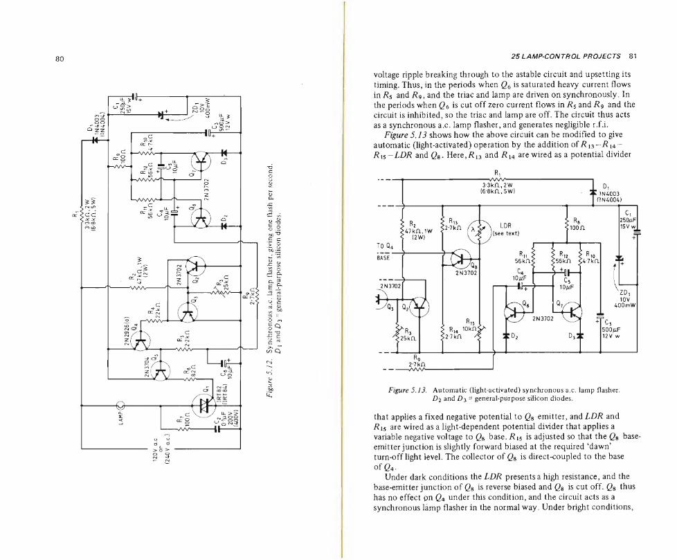
Fig
ure
5.1
2.
Synch
ronous
a.c. l
amp f
lash
er,
giv
ing o
ne
flas
h p
er s
econd.
D i
and £
>3 =
gen
eral
-pu
rpo
se S
ilic
on d
iod
es.
25 LAMP-CONTROL PROJECTS 81
voltage ripple breaking through to thè astable Circuit and upsetting its timing. Thus, in thè periods when Q6 is saturated heavy current flows in Rs and R9, and thè triac and lamp are driven on synchronously. In thè periods when Q6 is cut off zero current flows in Rs and R9 and thè Circuit is inhibited, so thè triac and lamp are off. The Circuit thus acts as a synchronous a.c. lamp flasher, and generates negligible r.f.i.
Figure 5.13 shows how thè above circuit can be modified to give automatic (light-activated) operation by thè addition of R i3 —R14-
R\s~LDR and Qs. Here,/?13 and Ru are wired as a potential divider
Ri
Figure 5.13. Automatic (light-activated) synchronous a.c. lamp flasher. Di and Z)3 = general-purpose Silicon diodes.
that applies a fixed negative potential to Q% emitter, and LDR and R i5 are wired as a light-dependent potential divider that applies a variable negative voltage to Q% base. R15 is adjusted so that thè Q% base- emitter junction is slightly forward biased at thè required ‘dawn’ turn-off light level. The collector of Q% is direct-coupled to thè base
of 04- Under dark conditions thè LDR presents a high resistance, and thè
base-emitter junction of Q% is reverse biased and Qs is cut off. Q% thus has no effect pn Q4 under this condition, and thè circuit acts as a
synchronous lamp flasher in thè normal way. Under bright conditions,
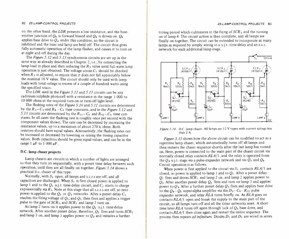
82 25 LAMP.CONTROL PROJECTS
on thè other hand, thè LDR presents a low resistance, and thè base- emitter junction of Q8 is forward biased and Q8 is driven on. Q8 applies base drive to Q4 under this condition, so thè Circuit is inhibited and thè triac and lamp are held off. The Circuit thus gives fully automatic operation of thè lamp flasher, and causes it to turn on at night and off during thè day.
The Figure 5.12 and 5.13 synchronous circuits are set up in thè same way as already described in Chapter 2, i.e., by connecting thè lamp load in place and then reducing thè R3 value until full-wave lamp
operation is just obtained. The voltage across C\ should be checked when 7? 3 is adjusted, to ensure that it does not fall appreciably below thè nominai 10 V value. The Circuit should only be used with lamp loads with total ratings in excess of a couple of hundred watts using thè specified triacs.
The LDR used in thè Figure 5.11 and 5.13 circuits can be any cadmium sulphide photocell with a resistance in thè range 1 000 to 10 000 ohms at thè required turn-on or turn-off light level.
The flashing rates of thè Figure 5.10 and 5.77 circuits are determined by thè 7^3-C3 and R4 — C4 time constants, and in thè Figure 5.12 and 5.13 circuits are determined by thqRu-Cs and/?i2-C4 time con¬ stants. In all cases thè flashing rate is roughly once per second with thè component values shown. The rate can be decreased by increasing thè resistance values, up to a maximum of about 270 k ohms. Both resistors should have equal values. Alternatively, thè flashing rates can be increased or decreased by lowering or raising thè timing capacitor values. Both capacitors should be given equal values, and can be in thè range 1 //F to 1 000 fiF.
D.C. lamp chaser projects
Lamp chasers are circuits in which a number of lights are arranged so that they turn on sequentially, with a preset time delay between each operation, until they are all finally on together. Figure 5.14 shows a practical d.c. chaser of this type.
Normally, with S\ open, all lamps and s.c.r.s are off, and all capacitors are discharged. When S\ is first closed power is applied to lamp 1 and to thè Q\ u.j.t. time-delay Circuit, and Cy starts to charge exponentially via/?i. Note at this stage that all s.c.r.s are off, so zero power is applied to thè Q2 or Q3 networks. After a preset delay
reaches thè firing voltage of gì, and Q\ then fires and applies a trigger pulse to thè gate ofSCRi, and SCR\ and lamp 2 turn on.
As lamp 2 turns on it applies power to thè Q2 u.j.t. time-delay network. After another preset delay, therefore, Q2 fìres and turns SCR2 and lamp 3 on, and lamp 3 applies power to Q3 and initiates a further
25 LAMP-CONTROL PROJECTS 83
timing period which culminates in thè firing of SCR3 and thè turning on of lamp 4. The circuit action is then complete, and all lamps are finally on together. The Circuit can be extended to incorporate as many lamps as required by simply wiring in a u.j.t. time-delay and an s.c.r. network for each additional lamp stage.
Figure 5.14. D.C. lamp chaser. All lamps are 12 V types with current ratings less than 2 A.
Figure 5.15 shows how thè above circuit can be modified to act as a repetitive lamp chaser, which automatically turns off all lamps and then restarts thè chaser sequence shortly after thè last lamp has turned on. Here, power is connected to thè main part of thè chaser circuit via normally closed relay contacts RLA/l, and thè relay is operated from thè Q$ u.j.t. stage via a pulse-expander network and via Q4 and Qs. Circuit operation is as follows.
When power is first applied to thè circuit via S\ contacts RLA/\ are closed, so power is applied to lamp 1 and to Q\. After a preset delay Qi fires and drives SCRi and lamp 2 on, and lamp 2 applies power to
Q2. After another preset delay Q2 fires and turn on lamp 3 and applies
power to Qs. After a further preset delay Qs fires and applies base drive
to thè Q4-Qs super-alpha amplifìer via thèDs-C4-Ri2 pulse expander network, and relay RLA turns briefly on. As RLA goes on contacts RLA/l open and break thè supply to thè main part of thè
circuit, so all lamps turn off and all thè timer networks reset. A short time hiexRLA turns off again through lack of Q4 base drive, and contacts RLA/l then dose again and restart thè entire sequence. The process then repeats ad infmitum. Diodes D\ and D2 are wired in series
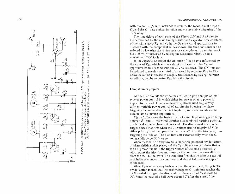
84
£
- s 2 S a rt *0 a)
Oj « c P *0 cd
SgS —• O vi — O <D
u 4> Q) W O
« O rt s ” M <«G
O 3 ;£
§ « >» ■2 o g 2
■o *°> S Va SQ n S.2^
oiQft:
<rJ'
■è E*,
25 LAMP-CONTROL PROJECTS 85
with/?n in thè Q3 u.j.t. network to counter thè forward volt drops of D3 and thè Qs base-emitter junction and ensure stable triggering of thè 12 V relay.
The time delays of each stage of thè Figure 5.14 and 5.15 circuits are determined by thè main timing resistor and capacitor time constants of thè u.j.t. stages (R1 and C{ in thè Q\ stage), and approximate to 1 second with thè component values shown. The time constants can be reduced by lowering thè timing resistor values, down to a minimum of 6-8 k ohms, or increased by raising thè resistance values, up to a maximum of 500 k ohms.
In thè Figure 5.15 Circuit thè ON time of thè relay is influenced by thè value of /?i3, which acts as a shunt discharge path for C4, and approximates to 1 second with thè /?i3 value shown. The ON time can
be reduced to roughly one third of a second by reducing/?i3 to 33 k ohms, or can be increased to roughly fìve seconds by raising thè value to infìnity, i.e., by removing/?i3 from thè Circuit.
Lamp dimmer projects
All thè triac circuits shown so far are used to give a simple on/off type of power control in which either full power or zero power is
applied to thè load. Triacs can, however, also be used to give very effìcient variable power control of a.c. circuits by using thè phase triggering technique described in Chapter 1, and such circuits can be
used in lamp dimming applications. Figure 5.16a shows thè basic Circuit of a simple phase-triggered lamp
dimmer. R ! and C\ are wired together as a combined variable potential divider and variable phase shift network. The diac is used as a simple trigger device that fìres when thè C\ voltage rises to roughly 35 V (in either polarity) and then partially discharges C\ into thè triac gate, thus
triggering thè triac on. The diac turns off automatically when thè C\ voltage falls below 30 V or so.
When/?i is set to a very low value negligible potential divider action or phase shifting takes place, and thè C\ voltage closely follows that of thè a.c. power line until thè trigger voltage of thè diac is reached, at which point thè triac fìres and turns on thè lamp and removes all drive from thè R\-C\ network. The triac thus fìres shortly after thè start of each half-cycle under this condition, and almost full power is applied
to thè load. When R\ is set to a very high value, on thè other hand, thè potential
divider action is such that thè peak voltage on C\ only just reaches thè 35 V needed to trigger thè diac, and thè phase shift of C\ is dose to 90°. Since thè peak of a half-wave occurs 90° after thè start of thè
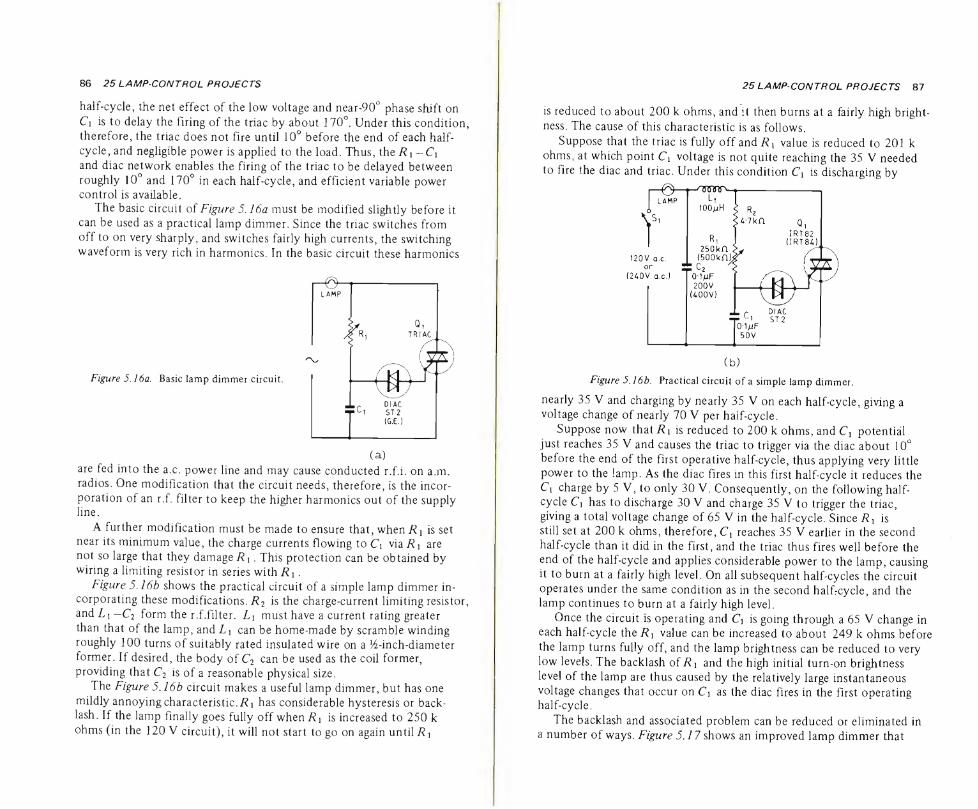
86 25 LAMP'CONTROL PROJECTS
half-cycle, thè net effect of thè low voltage and near-90° phase shift on
C\ is to delay thè fìring of thè triac by about 170°. Under this condition, therefore, thè triac does not Tire until 10° before thè end of each half- cycle, and negligible power is applied to thè load. Thus, thè RX~CX and diac network enables thè firing of thè triac to be delayed between roughly 10° and 170° in each half-cycle, and efficient variable power control is available.
The basic Circuit of Figure 5.16a must be modifìed slightly before it can be used as a practical lamp dimmer. Since thè triac switches from off to on very sharply, and switches fairly high currents, thè switching
waveform is very rich in harmonics. In thè basic Circuit these harmonics
Figure 5.16a. Basic lamp dimmer Circuit.
are fed into thè a.c. power line and may cause conducted r.f.i. on a.m. radios. One modifìcation that thè Circuit needs, therefore, is thè incor¬ poration of an r.f. filter to keep thè higher harmonics out of thè supply line.
A further modifìcation must be made to ensure that, when Ri is set near its minimum value, thè charge currents flowing to C\ via R x are not so large that they damage R i. This protection can be obtained by wiring a limiting resistor in series with Ri.
Figure 5.16b shows thè practical circuit of a simple lamp dimmer in- corporating these modifications. R2 is thè charge-current limiting resistor, and Lx-C2 form thè r.f.filter. Lx must have a current rating greater than that of thè lamp, and Li can be home-made by scramble winding roughly 100 turns of suitably rated insulated wire on a ^-inch-diameter former. If desired, thè body of C2 can be used as thè coil former, providing that C2 is of a reasonable physical size.
The Figure 5A6b circuit makes a useful lamp dimmer, but has one
mildly annoyingcharacteristic./?] has considerable hysteresis or back- lash. If thè lamp fìnally goes fully off when R\ is increased to 250 k ohms (in thè 120 V circuit), it will not start to go on again until/?]
25 LAMP-CONTROL PROJECTS 87
is reduced to about 200 k ohms, and it then burns at a fairly high bright-
ness. The cause of this characteristic is as follows.
Suppose that thè triac is fully off and/?] value is reduced to 201 k ohms, at which point Cx voltage is not quite reaching thè 35 V needed to fìre thè diac and triac. Under this condition Cx is discharging by
Figure 5.16b. Practical circuit of a simple lamp dimmer.
nearly 35 V and charging by nearly 35 V on each half-cycle, giving a voltage change of nearly 70 V per half-cycle.
Suppose now that /? i is reduced to 200 k ohms, and Cx potentiàl just reaches 35 V and causes thè triac to trigger via thè diac about 10° before thè end of thè first operative half-cycle, thus applying very little power to thè lamp. As thè diac fìres in this first half-cycle it reduces thè C\ charge by 5 V, to only 30 V. Consequently, on thè following half- cycle C\ has to discharge 30 V and charge 35 V to trigger thè triac, giving a total voltage change of 65 V in thè half-cycle. Since Rx is stili set at 200 k ohms, therefore, Cx reaches 35 V earlier in thè second half-cycle than it did in thè first, and thè triac thus fires well before thè end of thè half-cycle and applies considerable power to thè lamp, causing it to burn at a fairly high level. On all subsequent half-cycles thè circuit operates under thè same condition as in thè second half-cycle, and thè lamp continues to burn at a fairly high level.
Once thè circuit is operating and Ci is going through a 65 V change in each half-cycle thè Rx value can be increased to about 249 k ohms before thè lamp turns fully off, and thè lamp brightness can be reduced to very low levels. The backlash ofRx and thè high initial turn-on brightness level of thè lamp are thus caused by thè relatively large instantaneous voltage changes that occur on Ci as thè diac fìres in thè first operating half-cycle.
The backlash and associated problem can be reduced or eliminated in a number of ways. Figure 5.17 shows an improved lamp dimmer that
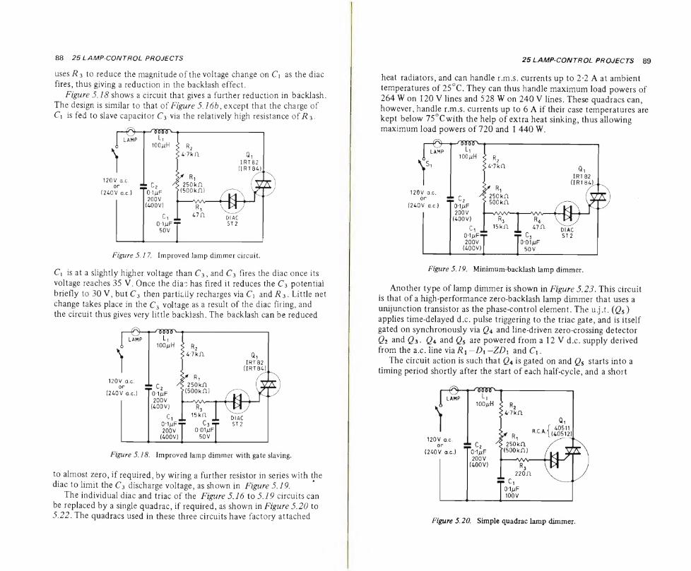
88 25 LAMP-CONTROL PROJECTS
uses R 3 to reduce thè magnitude of thè voltage change on C\ as thè diac fires, thus giving a reduction in thè backiash effect.
Figure 5.18 shows a circuit that gives a further reduction in backiash. The design is similar to that of Figure 5.16by except that thè charge of Ci is fed to slave capacitor C3 via thè relatively high resistance ofR$.
Figure 5.17. Improved lamp dimmer Circuit.
Ci is at a slightly higher voltage than C3, and C3 fires thè diac once its
voltage reaches 35 V. Once thè diac has fired it reduces thè C3 potential briefly to 30 V, but C3 then partially recharges via and R$. Little net change takes place in thè C3 voltage as a result of thè diac fìring, and thè circuit thus gives very little backiash. The backiash can be reduced
Figure 5.18. Improved lamp dimmer with gate slaving.
to almost zero, if required, by wiring a further resistor in series with thè diac to limit thè C3 discharge voltage, as shown in Figure 5.19.
The individuai diac and triac of thè Figure 5.16 to 5.19 circuits can be replaced by a single quadrac, if required, as shown in Figure 5.20 to 5.22. The quadracs used in these three circuits have factory attached
25 LAMP-CONTROL PROJECTS 89
heat radiators, and can handle r.m.s. currents up to 2*2 A at ambient
temperatures of 25°C. They can thus handle maximum load powers of 264 W on 120 V lines and 528 W on 240 V lines. These quadracs can, however, handle r.m.s. currents up to 6 A if their case temperatures are kept below 75°G with thè help of extra heat sinking, thus allowing maximum load powers of 720 and 1 440 W.
Figure 5.19. Minimum-backlash lamp dimmer.
Another type of lamp dimmer is shown in Figure 5.23. This circuit is that of a high-performance zero-backlash lamp dimmer that uses a unijunction transistor as thè phase-control element. The u.j.t. (Qs)
applies time-delayed d.c. pulse triggering to thè triac gate, and is itself gated on synchronously via QA and line-driven zero-crossing detector Qi and Q2. QA and Qs are powered from a 12 V d.c. supply derived from thè a.c. line via R j —Di —ZD\ and C\.
The circuit action is such that QA is gated on and Qs starts into a timing period shortly after thè start of each half-cycle, and a short
Figure 5.20. Simple quadrac lamp dimmer.
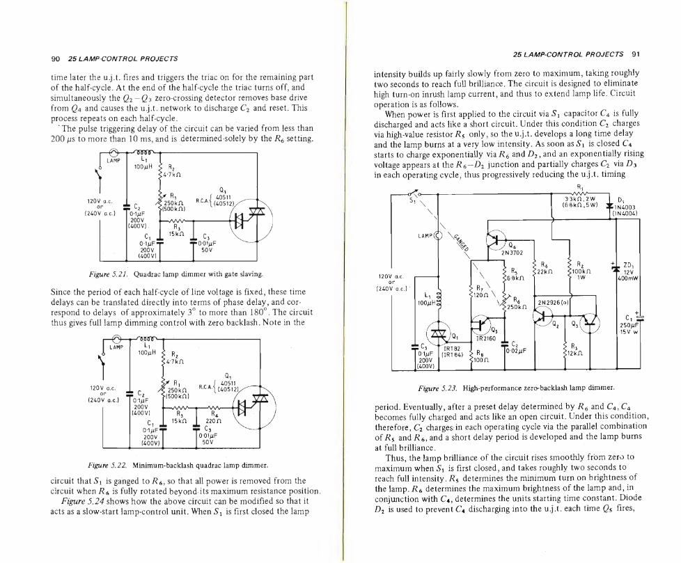
90 25 LAMP-CONTROL PROJECTS
time la ter thè u.j.t. fìres and triggers thè triac on for thè remaining part
of thè half-cycle. At thè end of thè half-cycle thè triac turns off, and simultaneously thè g2-g3 zero-crossing detector removes base drive
from Q4 and causes thè u.j.t. network to discharge C2 and reset. This process repeats on each half-cycle.
' The pulse triggering delay of thè Circuit can be varied from less than 200 /zs to more than 10 ms, and is determined-solely by thè Ró setting.
Figure 5.21. Quadrac lamp dimmer with gate slaving.
Since thè period of each half-cycle of line voltage is fixed, these time delàys can be translated directly into terms of phase delay, and cor- respond to delays of approximately 3° to more than 180°. The Circuit thus gives full lamp dimming control with zero backlash. Note in thè
Figure 5.22. Minimum-backlash quadrac lamp dimmer.
Circuit that S\ is ganged to /?6, so that all power is removed from thè Circuit when /?6 is fully rotated beyond its maximum resistance position.
Figure 5.24 shows how thè above circuit can be modifìed so that it acts as a slow-start lamp-control unit. When Sx is fìrst closed thè lamp
25 LAMP-CONTROL PROJECTS 91
intensity builds up fairly slowly from zero to maximum, taking roughly two seconds to reach full brilliance. The circuit is designed to eliminate high turn-on inrush lamp current, and thus to extend lamp life. Circuit
operation is as follows. When power is fìrst applied to thè circuit via S\ capacitor C4 is fully
discharged and acts like a short circuit. Under this condition C2 charges via high-value resistor R$ only, so thè u.j.t. develops a long time delay and thè lamp burns at a very low intensity. As soon as Si is closed C4 starts to charge exponentiaìly via/?6 and D2, and an exponentially rising
voltage appears at the/?6—D2 junction and partially charges C2 via D$ in each operating cycle, thus progressively reducing thè u.j.t. timing
Figure 5.23. High-performance zero-backlash lamp dimmer.
period. Eventually, after a preset delay determined by /?6 and C4, C4 becomes fully charged and acts like an open circuit. Under this condition, therefore, C2 charges; in each operating cycle via thè parallel combination of/?5 and/?6, and a short delay period is developed and thè lamp burns
at full brilliance. Thus, thè lamp brilliance of thè circuit rises smoothly from zero to
maximum when Si is fìrst closed, and takes roughly two seconds to reach full intensity. R$ determines thè minimum turn on brightness of thè lamp./?6 determines thè maximum brightness of thè lamp and, in conjunction with C4, determines thè units starting time Constant. Diode
D2 is used to prevent C4 discharging into thè u.j.t. each time Qs fìres,
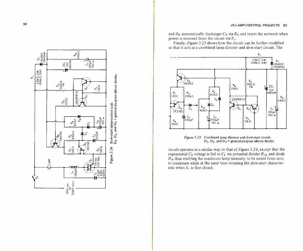
92
cn O
K è
25 LAMP-CONTROL PROJECTS 93
andD4 automatically discharges C4 via £9 and resets thè network when power is removed from thè Circuit via S{.
Finally, Figure 5,25 shows how thè Circuit can be further modified so that it acts as a combined lamp dimmer and slow-start Circuit. The
Figure 5,25. Combined lamp dimmer and slow-start Circuit. D2j D3, and D4 = general-purpose Silicon diodes.
Circuit operates in a similar way to that of Figure 5.24, except that thè exponential C4 voltage is fed to C2 via potential divider Rì0 and diode D3, thus enabling thè maximum lamp intensity to be varied from zero to maximum while at thè same time retaining thè slow-start character- istic when Si is first closed.
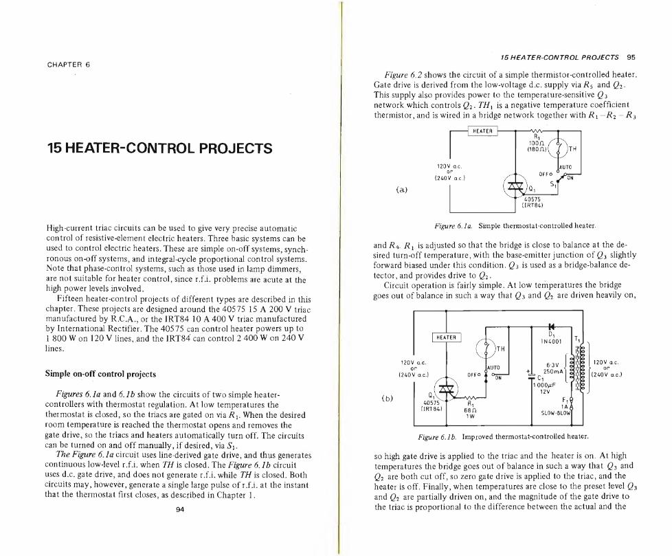
CHAPTER 6
15 HEATER-CONTROL PROJECTS
High-current triac circuits can be used to give very precise automatic
control of resistive-element electric heaters. Three basic systems can be
used to control electric heaters. These are simple on-off systems, synch-
ronous on-off systems, and integral-cycle proportional control systems. Note that phase-control systems, such as those used in lamp dimmers,
are not suitable for heater control, since r.f.i. problems are acute at thè high power levels involved.
Fifteen heater-control projects of different types are described in this chapter. These projects are designed around thè 40575 15 A 200 V triac manufactured by R.C.A., or thè IRT84 10 A 400 V triac manufactured by International Rectifier. The 40575 can control heater powers up to 1 800 W on 120 V lines, and thè IRT84’ can control 2 400 W on 240 V lines.
Simple on-off control projects
Figures 6. la and b.7£> show thè circuits of two simple heater- controllers with thermostat regulation. At low temperatures thè
thermostat is closed, so thè triacs are gated on via Rx. When thè desired room temperature is reached thè thermostat opens and removes thè
gate drive, so thè triacs and heaters automatically turn off. The circuits can be turned on and off manually, if desired, via S\.
The Figure 6Ja Circuit uses line-derived gate drive, and thus generates continuous low-level r.f.i. when TH is closed. The Figure 6.Ih Circuit uses d.c. gate drive, and does not generate r.f.i. while TH is closed. Both circuits may, howevèr, generate a single large pulse of r.f.i. at thè instant that thè thermostat First closes, as described in Chapter 1.
94
15 HEA TER-CONTROL PROJECTS 95
Figure 6.2 shows thè Circuit of a simple thermistor-controlled heater. Gate drive is derived from thè low-voltage d.c. supply via R5 and Q2. This supply also provides power to thè temperature-sensitive Q3 network which Controls Q2. THX is a negative temperature coefficient thermistor, and is wired in a bridge network together with Ri -R2 -R$
(a)
and R4. R ! is adjusted so that thè bridge is dose to balance at thè de¬ sired turn-off temperature, with thè base-emitter junction of Q3 slightly forward biased under this condition. Q$ is used as a bridge-balance de¬
tector, and provides drive to Q2. Circuit operation is fairly simple. At low temperatures thè bridge
goes out of balance in such a way that Q3 and Q2 are driven heavily on,
so high gate drive is applied to thè triac and thè heater is on. At high temperatures thè bridge goes out of balance in such a way that Q3 and
Q2 are both cut off, so zero gate drive is applied to thè triac, and thè heater is off. Finally, when temperatures are dose to thè preset level Q3 and Q2 are partially driven on, and thè magnitude of thè gate drive to
thè triac is proportional to thè difference between thè actual and thè
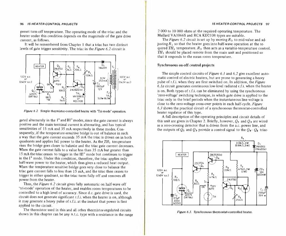
96 15 HEATER-CONTROL PROJECTS
preset turn-off temperature. The operating mode of thè triac and thè heater under this condition depends on thè magnitude of thè gate drive current, as follows.
It will be remembered from Chapter 1 that a triac has two distinct levels of gate trigger sensitivity. The triac in thè Figure 6.2 Circuit is
Figure 6.2. Simple thermistor-controUed heater with ‘Tri-mode’ operation.
gated alternately in thè I+ and III+ modes, since thè gate current is always positive and thè main terminal current is alternating, and has typical
sensitivities of 15 mA and 35 mA respectively in these modes. Con- sequently, if thè temperature-sensitive bridge is out of balance in such a way that thè gate current exceeds 35 mÀ thè triac is driven on in both quadrants and applies full power to thè heater. As thè THi temperature rises thè bridge goes closer to balance and thè triac gate current decreases. When thè gate current falls to a value less than 35 mA but greater than 15 mAthe triac ceases to trigger in thè III+ mode but continues to trigger in thè I+ mode. Under this condition, therefore, thè triac applies only half-wave power to thè heater, which thus gives a reduced heat output. When thè temperature sensitive bridge goes very dose to balance thè triac gate current falls to less than 15 mA, and thè triac then ceases to trigger in either quadrant, so thè triac turns fully off and removes all power from thè heater.
Thus, thè Figure 6.2 Circuit gives fully automatic on half-wave off
‘tri-mode’ operation of thè heater, and enables room temperatures to be controlled to a high level of accuracy. Since d.c. gate drive is used, thè Circuit does not generate signifìcant r.f.i. when thè heater is ón, although it may generate a heavy pulse of r.f.i. at thè instant that power is fìrst applied to thè Circuit.
The thermistor used in this and all other thermistor-regulated circuits
shown in this chapter can be any n.t.c. type with a resistance in thè range
15 HEA TER-CONTROL PROJECTS 97
2 000 to 10 000 ohms at thè required operating temperature. The Mullard VA1066S and RCA KD2108 types are suitable.
The Figure 6.2 Circuit is set up by moving R3 to mid-value and ad- justingi?! so that thè heater goes into half-wave operation at thè re¬ quired THX temperature. R3 then acts as a variable-temperature control. THi should be placed remote from thè main unit and positioned so that it responds to thè mean room temperature.
Synchronous on-off control projects
The simple control circuits of Figure 6.1 and 6.2 give excellent auto¬ matic control of electric heaters, but are prone to generating a heavy pulse of r.f.i. when they are fìrst switched on. In addition, thè Figure 6.la Circuit generates continuous low-level radiated r.f.i. when thè heater
is on. Both types of r.f.i. can be eliminated by using thè synchronous ‘zero-voltage’ switching technique, in which gate drive is applied to thè triac only in thè brief periods when thè instantaneous line voltage is
dose to thè zero-voltage cross-over points in each half-cycle. Figure 6.3 shows thè practical Circuit of a synchronous thermostat-controlled heater regulator of this type.
A full description of thè operating principles and Circuit details of
this unit are given in Chapter 2. Briefly, however, Q2 and Q$ are wired
as a zero-crossing detector that is driven from thè a.c. power line, and thè outputs of Q2 and Qi provide a control signal to thè Qs triac-
Ri
Figure 6.3. Synchronous thermostat-controUed heater.
98 15 HEATERCONTROL PROJECTS
gate-drive network. Q4 and Qs are powered from a 10 V d.c. supply derived from thè power line via R i -Di - Ci and zener diode ZDi.
The Circuit action is such that a heavy pulse of gate drive is applied to thè triac only when thè instantaneous line voltage is dose to zero at thè cross-over points near thè beginning and end of each half-cycle, and when base drive is available to Q4 via Rs. The Circuit thus gives r.f.i.- free operation of thè heater, and can be inhibited or turned off by simply removing thè R5 current. In Figure 6.3 thermostat TH is wired
in series with Rs, and thus gives automatic on-off control of thè heater.
At low temperatures thè thermostat is closed and thè Circuit gives synchronous operation of thè heater. At high temperatures thè thermo¬ stat is open and thè Circuit is inhibited, so thè heater is off. The Circuit can be turned on and off manually, if required, via Si.
The Figure 6.3 Circuit is very easy to set up, since R3 is thè only adjustable component in thè design (apart from thè thermostat). It should be noted, however, that (as pointed out in Chapter 2) this component must be adjusted to suit thè particular resistive load that is used with thè triac. If a multi-value load, such as a two or three-bar heater, is used, thè ^3 adjustment must be made with thè load in its
minimum-load position, i.e., with only one of thè heater bars turned on. Once thè initial^a adjustment has been made thè Circuit will function correctly in all positions of thè multi-value load.
The R3 adjustment is in practice very simple. The selected heater is simply connected in place (turned to its minimum load position),
R* is set to give maximum resistance, and SY is turned to thè ON position. The ^3 value is then gradually reduced until it is just past
thè point at which thè heater turns full on; thè adjustment is then
complete. The voltage across Ci should be checked when ^3 is adjusted, to ensure that it does not fall below thè nominai 10 V value. The Circuit is then ready for use.
Figures 6.4 and 6.5 show how thè basic synchronous control Circuit can be modified to give thermistor regulation of thè heater. In thè Figure 6.4 Circuit R$ —R9 — R10—Rn and thermistor 77/iare wired as a temperature-sensitive bridge, and Q6 is wired as a simple bridge- balance detector similar to that used in thè Figure 6.2 Circuit. The Figure 6.5 Circuit is similar, except that differential amplifìer Q^ — Qi is used as thè bridge-balance detector.
In both cases thè Circuit action is such that Q$ is driven hard on when room temperatures are low, in which case current is available to ^5, so thè triac turns on synchronously and applies full power to thè heater. When temperatures are high, on thè other hand, Q6 is fully cut off and zero current flows in , so thè Circuit is inhibited and zero power is fed to thè heater. Finally, when temperatures are dose to thè
15 HE A TER-CONTROL PROJECTS 99
preset value Q& is driven partially on, and thè magnitudes of both thè Rs and thè triac-gate-drive currents are proportional to thè difference
between thè actual and thè preset temperatures. The triac is gated alternately in thè I"and III" modes, so tri-mode operation of thè heater is given under this condition. The circuits thus give excellent
Figure 6.4. Synchronous thermistor-controlled heater.
regulation of room temperature. The regulation of thè Figure 6.5 circuit
is slightly better than that of Figure 6.4, since thè operating point of
Figure 6.4 is influenced by thermally generated shifts in thè Vhe potential of Q&, while thè Figure 6.5 differential circuit is ùnaffected
by such changes.
The procedure for setting up thè two circuits is identical. First, connect thè heater in place, set S\ to thè ON position, and then adjust ^3 in thè same way as described for thè Figure 6.3 circuit. Next, set R9 to mid-value, raise THi to thè required turn-off temperature, and then adjust ^uso that thè heater goes into half-wave operation under this condition. All adjustments are then complete, and thè circuits are ready for use. R9 enables thè tum-off temperature to be varied a few
degrees ab out thè value preset by Rn. Finally,Figure 6.6 and 6.7 show how thè PA424 integrated circuit
described in Chapter 2 can be used for synchronous on-off heater- control. In thè Figure 6.6 circuit a thermostat is coupled to thè i.c.s differential amplifìer input via Rt —R% and ^4, and thè circuit action is such that thè triac is turned on synchronously when thè thermostat is closed, but is off when thè thermostat is open.
100 15 HE A TER-CONTROL PROJECTS
In thè Figure 6.7 Circuit a thermistor and variable resistor are wired to thè amplifier input, and thè Circuit Works in thè same way as that of
Figure 6.5. The triac is turned on synchronously at low temperatures, is off at high temperatures, and is operated in thè synchronous tri-mode at temperatures very dose to thè pre-set value.
R,
Figure 6.5. Alternative synchronous thermistor-controlled heater.
Integral-cycle variable-power projects
All thè circuits that we have looked at so far give a simple on-off
control of electric heaters, and thus give only a coarse control of heat output . Fully variable r.f.i.-free control of heater output can be
Figure 6.6. Synchronous thermostat-controUed heater using i.c.
15 HE A TER-CONTROL PROJECTS 101
obtained by using a synchronous integral-cycle triac switching technique, in which power is applied to thè heater for only a definite integrai number of half-cycles out of (say) every one hundred. Thus, if power is applied for only fifty half-cycles in each hundred thè heater will operate at 50 per cent of full power, and if power is applied for ninety half-cycles in every hundred it will operate at 90 per cent of full power, and so on.
Figure 6.1. Synchronous thermistor-controlled heater using i.c.
Figure 6.8 shows thè practical Circuit of an integral-cycle variable- power heater controller. Circuit operation is fairly simple. Qi~Q%- Qt-Qs are wired as a normal synchronous controller, and Q$-Qn are wired as an astable (free-running) multivibrator that applies a rectangular on-off control signal to R$. The astable action is such that Q6 and Qn switch on and off repetitively in opposition to one another. When Q6 is
on, base drive is applied to Qs via Rs, and thè triac is turned on synchronously. When Q6 is off all base drive is removed from and thè triac is off. The astable multivibrator has a total cycling period of approximately one second, and its mark-space ratio is fully variable
between 11:1 and 1:11 via Ri2. Consequently, thè heater power is fully variable between approximately 8 per cent and 92 per cent of
maximum via Rn. The heater can be turned fully off or fully on via
Si, if required. The manually operated variable-power facility can be readily added
to any of thè synchronous control circuits described earlier by simply adding thè multivibrator and a suitable selector switch to these designs,
so that they can be made to give either automatic or manual control via thè selector switch. Figures 6.9 and 6.10 show how thè circuits of
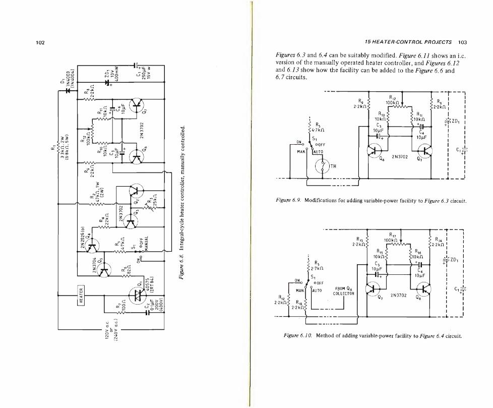
102
Fig
ure
6.8
. In
tegra
l-cy
cle
heate
r contr
oll
er, m
anu
ally
co
ntr
oll
ed.
15 HEATER-CONTROL PROJECTS 103
Fìgures 6.3 and 6.4 can be suitably modified. Figure 6.11 shows an i.c. version of thè manually operated heater controller, and Figures 6.12 and 6.13 show how thè facility can be added to thè Figure 6.6 and 6.7 circuits.
Figure 6.9. Modiflcations for adding variable-power facility to Figure 6.3 Circuit.
Figure 6.10. Method of adding variable-power facility to Figure 6.4 Circuit.
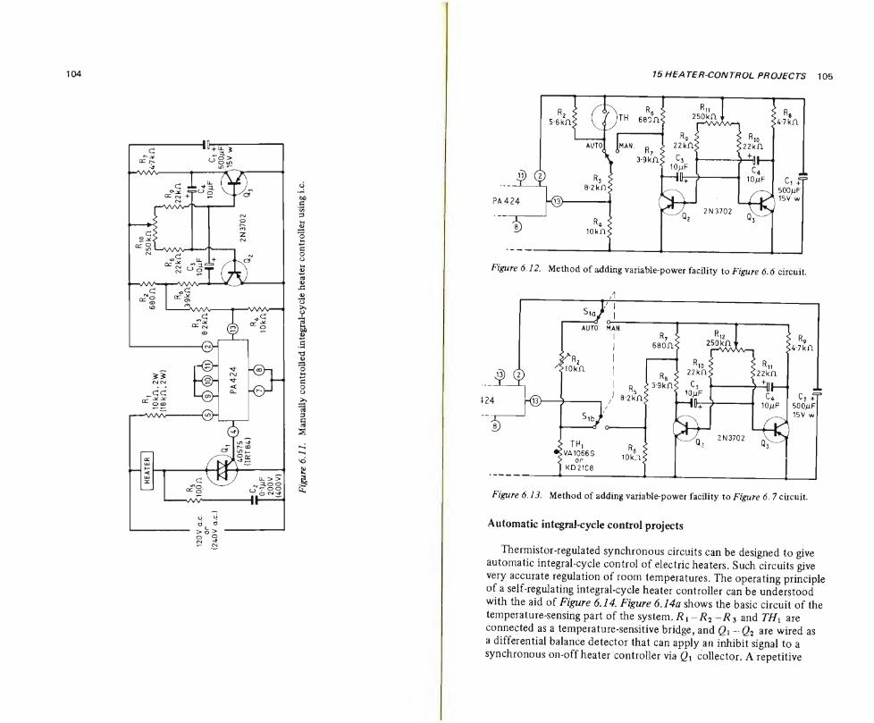
104
ci
e*
3
15 HE A TER-CON TROL PROJECTS 105
Figure 6.13. Method of adding vaiiable-power facility to Figure 6.7 Circuit.
Automatic integral-cycle control projects
Thermistor-regulated synchronous circuits can be designed to give automa tic integral-cycle control of electric heaters. Such circuits give very accurate regulation of room temperatures. The operating principle of a self-regulating integral-cycle heater controller can be understood with thè aid of Figure 6,14. Figure 6.14a shows thè basic Circuit of thè temperature-sensing part of thè System. Rx ~R2 -Rz and THX are connected as a temperature-sensitive bridge, and Q\ are wired as a differential balance detector that can apply an inhibit signal to a
synchronous on-off heater controller via Q\ collector. A repetitive
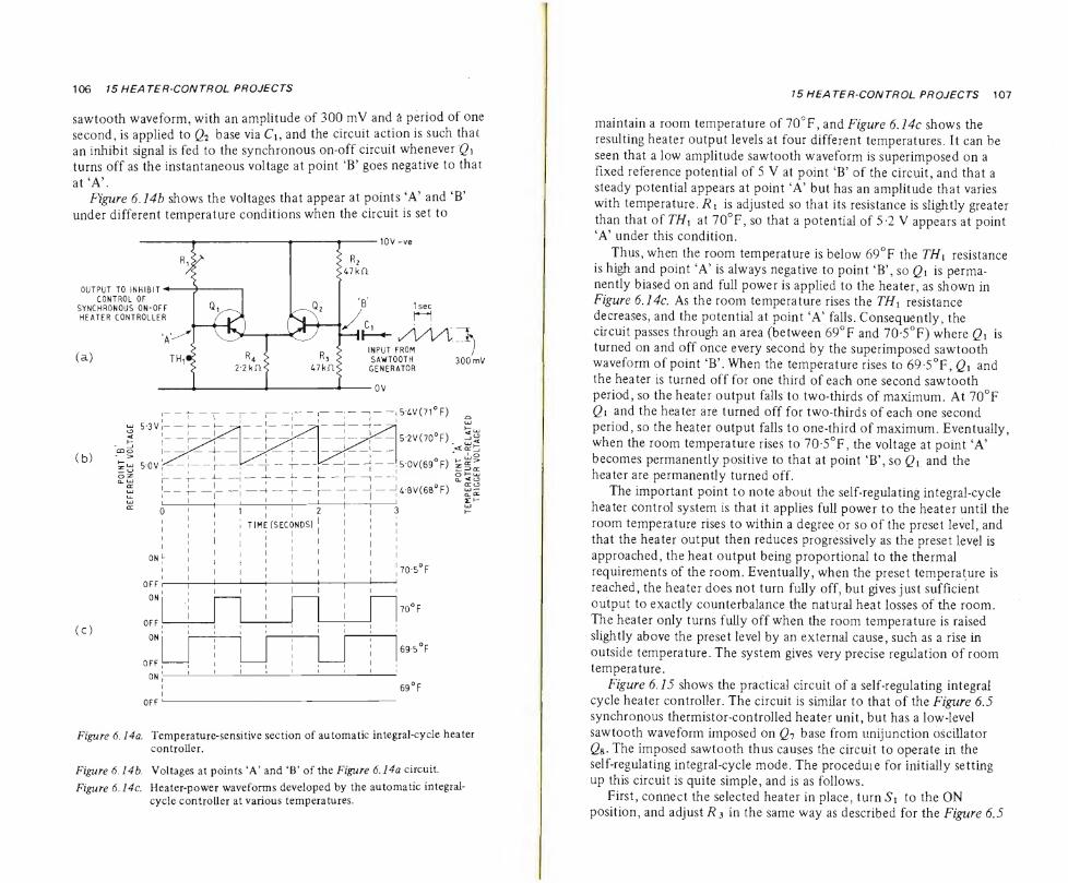
106 15 HEATER-CONTROL PROJECTS
sawtooth waveform, with an amplitude of 300 mV and à period of one second, is applied to g2 base via Ci, and thè Circuit action is such that an inhibit signal is fed to thè synchronous on-off Circuit whenever gì turns off as thè instantaneous voltage at point ‘ET goes negative to that
at ‘A’. Figure 6.14b shows thè voltages that appear at points ‘A’ and ‘B’
under different temperature conditions when thè Circuit is set to
Figure 6.14a. Temperature-sensitive section of automatic integral-cycle heater controller.
Figure 6.14b. Voltages at points ‘A’ and ‘B’ of thè Figure 6.l4a Circuit
Figure 6.14c. Heater-power waveforms developed by thè automatic integral- cycle controller at various temperatures.
15 HEATE R-CONTROL PROJECTS 107
maintain a room temperature of 70° F, and Figure 6.14c shows thè resulting heater output levels at four different temperatures. It can be seen that a low amplitude sawtooth waveform is superimposed on a Fixed reference potential of 5 V at point ‘B’ of thè Circuit, and that a steady potential appears at point ‘A’ but has an amplitude that varies
with temperature, is adjusted so that its resistance is slightly greater
than that of TH\ at 70°F, so that a potential of 5-2 V appears at point ‘A’ under this condition.
Thus, when thè room temperature is below 69°F thè THV resistance is high and point ‘A’ is always negative to point ‘B’, so gì is perma¬ nenti biased on and full power is applied to thè heater, as shown in Figure 6.14c. As thè room temperature rises thè THi resistance decreases, and thè potential at point ‘A’ falls. Consequently, thè Circuit passes through an area (between 69°F and 70*5°F) where gì is turned on and off once every second by thè superimposed sawtooth waveform of point ‘B\ When thè temperature rises to 69-5°F, g, and thè heater is turned off for one third of each one second sawtooth period, so thè heater output falls to two-thirds of maximum. At 70°F gì and thè heater are turned off for two-thirds of each one second period, so thè heater output falls to one-third of maximum. Eventuali, when thè room temperature rises to 70-5°F, thè voltage at point ‘A’ becomes permanenti positive t0 that at point ‘B’, so gì and thè heater are permanenti turned off.
The important point to note aboiit thè self-regulating integral-cycle heater control System is that it applies full power to thè heater until thè room temperature rises to within a degree or so of thè preset level, and that thè heater output then reduces progressively as thè preset level is
approached, thè heat output being proportional to thè thermal requirements of thè room. Eventuali, when thè preset temperature is reached, thè heater does not turn fully off, but gives just sufficient
output to exactly counterbalance thè naturai heat losses of thè room.
The heater only turns fully off when thè room temperature is raised
slightly above thè preset level by an external cause, such as a rise in
outside temperature. The System gives very precise regulation of room temperature.
Figure 6.15 shows thè practical Circuit of a self-regulating integrai cycle heater controller. The Circuit is similar to that of thè Figure 6.5 synchronous thermistor-controlled heater unit, but has a low-level sawtooth waveform imposed on g7 base from unijunction oscillato gg. The imposed sawtooth thus causes thè circuit to operate in thè self-regulating integral-cycle mode. The procedui e for initially setting up this circuit is quite simple, and is as follows.
First, connect thè selected heater in place, turn Si to thè ON position, and adjusti?3 in thè same way as described for thè Figure 6.5
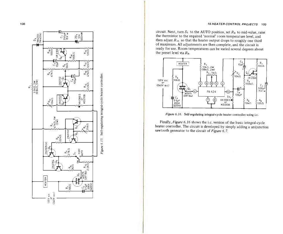
-M
V-
1 3-
3kA
,2W
Di
(6'8
kA,5
W)
3 *
1N40
03
(IN
4004)
Fig
ure
6.1
5.
Sel
f-re
gula
ting i
nte
gra
l-cy
cle
heate
r co
ntr
oll
er.
15 HEA TER CONTROL PROJECTS 109
Circuit. Next, turn Si to thè AUTO position, set R9 to mid-value, raise thè thermistor to thè required ‘normal’ room temperature level, and then adjust Ru so that thè heater output drops to roughly one third of maximum. All adjustments are then complete, and thè Circuit is ready for use. Room temperatures can be varied several degrees about thè preset level via R9.
Figure 6.16. Self-regulating integral-cycle heater controller using Le.
Finally, Figure 6.16 shows thè i.c. version of thè basic integral-cycle heater controller. The circuit is developed by simply adding a unijunction sawtooth generator to thè circuit of Figure 6.7.
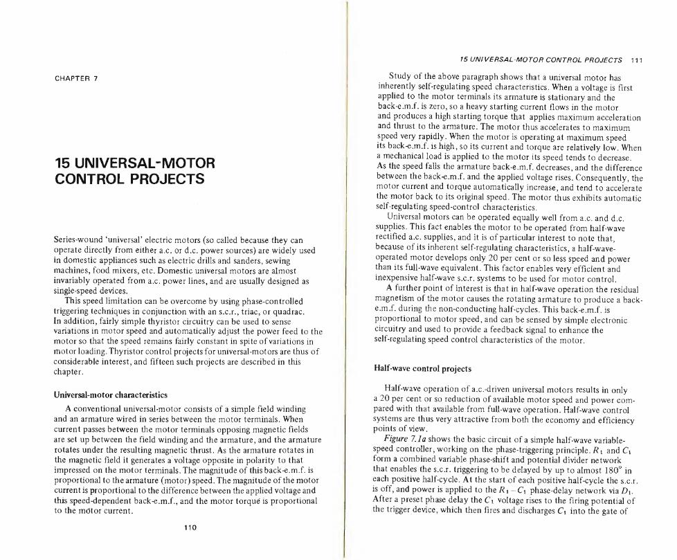
CHAPTER 7
15 UNIVERSAL-MOTOR CONTROL PROJECTS
Series-wound ‘universal’ electric motors (so called because they can
operate directly from either a.c. or d.c. power sources) are widely used in domestic appliances such as electric drills and sanders, sewing
machines, food mixers, etc. Domestic universal motors are aimost invariably operated from a.c. power lines, and are usually designed as single-speed devices.
This speed limitation can be overcome by using phase-controlled
triggering techniques in conjunction with an s.c.r., triac, or quadrac. In addition, fairly simple thyristor circuitry can be used to sense variations in motor speed and automatically adjust thè power feed to thè motor so that thè speed remains fairly Constant in spite of variations in
motor loading. Thyristor control projects for universal-motors are thus of considerable interest, and fìfteen such projects are described in this chapter.
Universal-motor characteristics
A conventional universal-motor consists of a simple field winding and an armature wired in series between thè motor terminals. When current passes between thè motor terminals opposing magnetic fields
are set up between thè field winding and thè armature, and thè armature
rotates under thè resulting magnetic thrust. As thè armature rotates in thè magnetic field it generates a voltage opposite in polarity to that impressed on thè motor terminals. The magnitude of this back-e.m.f. is proportional to thè armature (motor) speed. The magnitude of thè motor
current is proportional to thè difference between thè applied voltage and
this speed-dependent back-e.m.f., and thè motor torqué is proportional to thè mOtor current.
no
15 UN! VERSAL-MOTOR CONTROL PROJECTS 111
Study of thè above paragraph shows that a universal motor has inherently self-regulating speed characteristics. When a voltage is first applied to thè motor terminals its armature is stationary and thè back-e.m.f. is zero, so a heavy starting current flows in thè motor and produces a high starting torque that applies maximum acceleration and thrust to thè armature. The motor thus accelerates to maximum speed very rapidly. When thè motor is operating at maximum speed its back-e.m.f. is high, so its current and torque are relatively low. When a mechanical load is applied to thè motor its speed tends to decrease. As thè speed falls thè armature back-e.m.f. decreases, and thè difference between thè back-e.m.f. and thè applied voltage rises. Consequently, thè motor current and torque automatically increase, and tend to accelerate thè motor back to its originai speed. The motor thus exhibits automatic self-regulating speed-control characteristics.
Universal motors can be operated equally well from a.c. and d.c. supplies. This fact enables thè motor to be operated from half-wave rectified a.c. supplies, and it is of particular interest to note that,
because of its inherent self-regulating characteristics, a half-wave-
operated motor develops only 20 per cent or so less speed and power than its full-wave equivalent. This factor enables very effìcient and
inexpensive half-wave s.c.r. Systems to be used for motor control.
A further point of interest is that in half-wave operation thè residuai
magnetism of thè motor causes thè rotating armature to produce a back- e.m.f. during thè non-conducting half-cycles. This back-e.m.f. is
proportional to motor speed, and can be sensed by simple electronic circuitry and used to provide a feedback signal to enhance thè
self-regulating speed control characteristics of thè motor.
Half-wave control projects
Half-wave operation of a.c.-driven universal motors results in only a 20 per cent or so reduction of available motor speed and power com- pared with that available from full-wave operation. Half-wave control Systems are thus very attractive from both thè economy and effìciency points of view.
Figure 7. la shows thè basic Circuit of a simple half-wave variable- speed controller, working on thè phase-triggering principle. Ri and C\ form a combined variable phase-shift and potential divider network that enables thè s.c.r. triggering to be delayed by up to aimost 180° in each positive half-cycle. At thè start of each positive half-cycle thè s.c.r. is off, and power is applied to thè Ri - Ci phase-delay network via Di.
After a preset phase delay thè C\ voltage rises to thè fìring potential of thè trigger device, which then fìres and discharges C\ into thè gate of
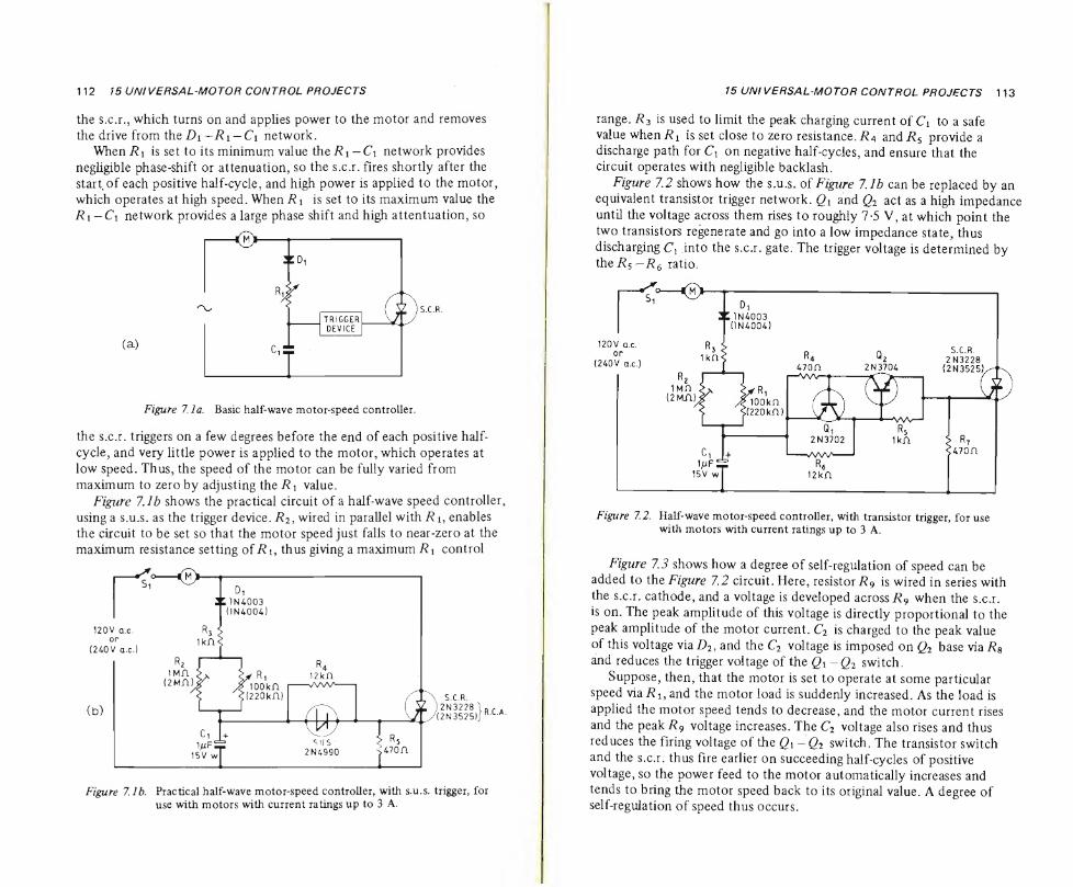
112 75 UNÌVERSAL-MOTOR CONTROL PROJECTS
thè s.c.r., which turns on and applies power to thè motor and removes thè drive from thè Di —R1 — Ci network.
When/?i is set to its minimum value the/?i-Ci network provides negligible phase-shift or attenuation, so thè s.c.r. fires shortly after thè start of each positive half-cycle, and high power is applied to thè motor, which operates at high speed. When Ri is set to its maximum value thè Ri—Ci network provides alarge phase shift and high attentuation, so
Figure 7Aa. Basic half-wave motor-speed controller.
thè s.c.r. triggers on a few degrees before thè end of each positive half- cycle, and very little power is applied to thè motor, which operates at low speed. Thus, thè speed of thè motor can be fully varied from
maximum to zero by adjusting thè R\ value. Figure 7.1b shows thè practical Circuit of a half-wave speed controller,
using a s.u.s. as thè trigger device. /?2, wired in parallel with R i, enables thè Circuit to be set so that thè motor speed just falls to near-zero at thè maximum resistance setting ofRi, thus giving a maximum Ri control
Figure 7Ab. Practical half-wave motor-speed controller, with s.u.s. trigger, for use with motors with current ratings up to 3 A.
75 UNÌ VERSAL-MOTOR CONTROL PROJECTS 113
range. R3 is used to limit thè peak charging current of Ci to a safe value when is set dose to zero resistance. Ra and Rs provide a discharge path for Cx on negative half-cycles, and ensure that thè Circuit operates with negligible backlash.
Figure 7.2 shows how thè s.u.s. of Figure 7.1b can be replaced by an equivalent transistor trigger network. Qi and Q2 act as a high impedance until thè voltage across them rises to roughly 7*5 V, at which point thè two transistors regenerate and go into a low impedance state, thus
discharging Cx into thè s.c.r. gate. The trigger voltage is determined by the/?5-/?6 ratio.
Figure 7.2. Half-wave motor-speed controller, with transistor trigger, for use with motors with current ratings up to 3 A.
Figure 7.3 shows how a degree of self-regulation of speed can be added to thè Figure 7.2 circuit. Here, resistor/?9 is wired in series with thè s.c.r. cathode, and a voltage is developed across R9 when thè s.c.r. is on. The peak amplitude of this voltage is directly proportional to thè peak amplitude of thè motor current. C2 is charged to thè peak value
of this voltage via Z)2, and thè C2 voltage is imposed on Q2 base via Rg and reduces thè trigger voltage of thè Qx -Q2 switch.
Suppose, then, that thè motor is set to operate at some particular speed via/?!, and thè motor load is suddenly increased. As thè load is applied thè motor speed tends to decrease, and thè motor current rises and thè peak/?9 voltage increases. The C2 voltage also rises and thus reduces thè firing voltage of thè Qi -Q2 switch. The transistor switch and thè s.c.r. thus fire earlier on succeeding half-cycles of positive voltage, so thè power feed to thè motor automatically increases and tends to bring thè motor speed back to its originai value. A degree of self-regulation of speed thus occurs.
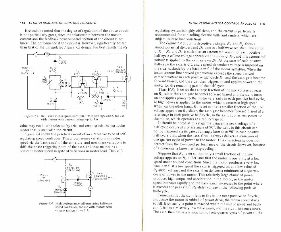
114 15 UNIVERSAL-MOTOFt CONTROL PROJECTS
It should be noted that thè degree of regulation of thè above Circuit is not particularly great, sirice thè relationship between thè motor current and thè feedback power-control section of thè Circuit is not linear. The performance if thè Circuit is, however, significantly better than that of thè unregulated Figure 7.2 design. For best results the/?9
Figure 7.3. Half-wave motor-speed controller, with self-regulation, for use with motors with current ratings up to 3 A.
value may need to be selected by trial and error to suit thè particular
motor that is used with thè Circuit. Figure 7.4 shows thè practical Circuit of an alternative type of self-
regulating speed controller. This Circuit senses variations in motor speed via thè back-e.m.f. of thè armature, and uses these variations to shift thè phase-triggering point of thè s.c.r. and thus maintains a
Constant motor speed in spite of variations in motor load. This self-
S.C.R. 2N3228 \
(2N3525)/ R.C.A.
Figure 7.4. High performance self-regulatìng half-wave speed controller, for use with motors with current ratings up to 3 A.
15 UNI VERSAL-MOTOR CONTROL PROJECTS 115
regulating System is highly efficient, and thè Circuit is particularly
recommended for controlling electric drills and sanders, which are subject to large load variations.
The Figure 7.4 Circuit is deceptively simple. Rx and R2 form a
simple potential divider, and Di acts as a half-wave rectifier. The action ofR\—R2 and Di is such that an attenuated version of each positive half-cycle of line voltage appears on thè slider of R2, and this attenuated voitage is applied to thè s.c.r. gate via D2. At thè start of each positive
half-cycle thè s.c.r. is off, and a speed-dependent voltage is imposed on thè s.c.r. cathode by thè back-e.m.f. of thè motor armature. When thè
instantaneous line-derived gate voltage exceeds thè speéd-derived cathode voltage in each positive half-cycle D2 and thè s.c.r. gate become forward biased, and thè s.c.r. then triggers on and applies power to thè motor for thè remaining part of thè half-cycle.
Thus, i[R2 is set so that a large fraction of thè line voltage appears onR2 slider thè s.c.r. gate becomes forward biased and thè s.c.r. turns
on and applies power to thè motor very early in each positive half-cycle, so high power is applied to thè motor, which operates at high speed. When, on thè other hand, R2 is set so that a smaller fraction of thè line voltage appears on R2 slider, thè s.c.r. gate becomes forward biased at a later stage in each positive half-cycle, so thè s.c.r. applies less power to thè motor, which operates at a reduced speed.
It should be noted at this stage that, since thè peak voltage of a half-cycle occurs at a phase angle of 90°, thè s.c.r. in this circuit can not be triggered via its gate at an angle later than 90° in each positive half-cycle. I.E., when thè s.c.r. fires, it always delivers a minimum of one quarter-cycle of power to thè motor. This characteristic does not
detract from thè low-speed performance of thè circuit, however, because of a phenomena known as ‘skip-cycling’.
Suppose that R2 is set so that only a small fraction of thè line voltage appears on R2 slider, and that thè motor is operating at a low speed under no-load conditions. Since thè motor produces a very low back-e.m.f. at a low speed thè s.c.r. is triggered on at a low value of /?2-slider voltage, and thè s.c.r. then delivers a minimum of a quarter- cycle of power to thè motor. This relatively large chunk of power produces high torque and acceleration in thè motor, so thè motor
speed increases rapidly and thè back-e.m.f. increases to thè point where it exceeds thè peak (90°) R2 -slider voltage in thè following positive half-cycle.
Consequently, thè s.c.r. fails to fire in thè next positive half-cycle, and, since thè motor is robbed of power drive, thè motor speed starts to fall. Eventually, a point is reached where thè motor speed and back- e.m.f. fall to a relatively low value again, and thè s.c.r. fires once more. The s.c.r. then delivers a minimum of one quarter-cycle of power to thè
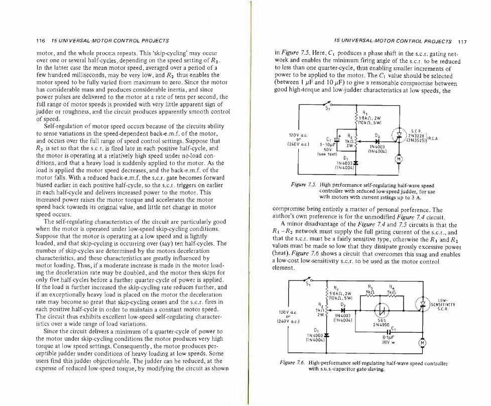
116 15 UNfVERSAL’MOTOR CONTROL PROJECTS
motor, and thè whole process repeats. This ‘skip-cycling’ may occur over one or several half-cycles, depending on thè speed setting of R2. In thè latter case thè mean motor speed, averaged over a period of a few hundred milliseconds, may be very low, and R2 thus enables thè motor speed to be fully varied from maximum to zero. Since thè motor has considerable mass and produces considerable inertia, and since power pulses are delivered to thè motor at a rate of tens per second, thè full range of motor speeds is provided with very little apparent sign of judder or roughness, and thè Circuit produces apparently smooth control of speed.
Self-regulation of motor speed occurs because of thè circuits ability to sense variations in thè speed-dependent back-e.m.f. of thè motor, and occurs over thè full range òf speed control settings. Suppose that R2 is set so that thè s.c.r. is fìred late in each positive half-cycle, and thè motor is operating at a relatively high speed under no-load con- ditions, and that a heavy load is suddenly applied to thè motor. As thè load is applied thè motor speed decreases, and thè back-e.m.f. of thè motor falls. With a réduced back-e.m.f. thè s.c.r. gate becomes forward biased earlier in each positive half-cycle, so thè s.c.r. triggers on earlier in each half-cycle and delivers increased power to thè motor. This increased power raises thè motor torque and accelerates thè motor speed back towards its originai value, and little net change in motor speed occurs.
The self-regulating characteristics of thè Circuit are particularly good when thè motor is operated under low-speed skip-cycling conditions. Suppose that thè motor is operating at a low speed and is lightly loaded, and that skip-cycling is occurring over (say) ten half-cycles. The number of skip-cycles are determined by thè motors deceleration characteristics, and these characteristics are greatly influenced by motor loading. Thus, if a moderate increase is made in thè motor load- ing thè deceleration rate may be doubled, and thè motor then skips for only rive half-cycles before a further quarter-cycle of power is applied. If thè load is further increased thè skip-cycling rate reduces further, and
if an exceptionally heavy load is placed on thè motor thè deceleration rate may become so great that skip-cycling ceases and thè s.c.r. fires in each positive half-cycle in order to maintain a Constant motor speed.
The Circuit thus exhibits excellent low-speed self-regulating character¬ istics over a wide range of load variations.
Since thè Circuit delivers a minimum ofa quarter-cycle of power to thè motor under skip-cycling conditions thè motor produces very high torque at low speed settings. Consequently, thè motor produces per- ceptible judder under conditions of heavy loading at low speeds. Some
users find this judder objectionable. The judder can be reduced, at thè expense of reduced low-speed torque, by modifying thè Circuit as shown
15 UNI VERSA L -MOTOR CONTROL PR OJECTS 117
in Figure 7.5. Here, Cx produces a phase shift in thè s.c.r. gating net¬ work and enables thè minimum firing angle of thè s.c.r. to be reduced
to less than one quarter-cycle, thus enabling smaller increments of power to be applied to thè motor. The Ci value should be selected (between 1 fiF and 10 (iF) to give a reasonable compromise between good high-torque and low-judder characteristics at low speeds, thè
Figure 7.5. High performance self-regulating half-wave speed controller with reduced low-speed judder, for use with motors with current ratings up to 3 A.
compromise being entirely a matter of personal preference. The
author’s own preference is for thè unmodifìed Figure 7.4 Circuit.
A minor disadvantage of thè Figure 7.4 and 7.5 circuits is that thè Ri -R2 network must supply thè full gating current of thè s.c.r., and that thè s.c.r. must be a fairly sensitive type, otherwise thè Rx and/?2 values must be made so low that they dissipate grossly excessive power
(heat). Figure 7.6 shows a Circuit that overcomes this snag and enables a low-cost low-sensitivity s.c.r. to be used as thè motor control element.
Figure 7.6. High-performance self-regulating half-wave speed controller with s.u.s.-capacitor gate-slaving.
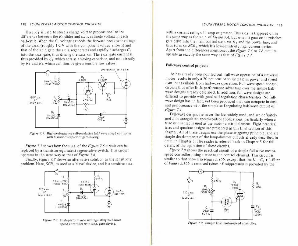
118 15 UN1VERSAL-MOTOR CONTROL PROJECTS
Here, C\ is used to store a charge voltage proportional to thè difference between the/^-slider and s.c.r. cathode voltage in each half-cycle. When thè C\ voltage exceeds thè forward breakover voltage
of thè s.u.s. (roughly 1*2 V with thè component values shown) and
that of thè s.c.r. gate thè s.u.s. regenerates and rapidly discharges C\ into thè s.c.r. gate, thus driving thè s.c.r. on. The s.c.r. gate current is
thus provided by Cu which acts as a slaving capacitar, and not directly
by Ri and R2> which can thus be given sensibly low values.
Figure 7.7. High-performance self-regulating half-wave speed controller with transistor-capacitor gate-slaving.
Figure 7.7 shows how thè s.u.s. of thè Figure 7.6 Circuit can be
replaced by a transistor-equivalent regenerative switch. This Circuit
operates in thè same way as that of Figure 7.6. Finally, Figure 7.8 shows an alternative solution to thè sensitivity
problem. Here, SCRi is used as a ‘slave’ device, and is a sensitive s.c.r.
Figure 7.8. High-performance self-regulating half-wave speed controller with s.c.r. gate-slaving.
15 UN! VERSAL-MOTOR CONTROL PROJECTS 119
with a current rating of 1 amp or greater. This s.c.r. is triggered on in thè same way as thè s.c.r. of Figure 7.4, but when it goes on it switches gate drive mto thè main control s.c.r. via Rz and thè power line, and thus turns on SCR2, which is a low-sensitivity high-current device. Apart from thè differences mentioned, thè Figure 7.6 to 7.8 circuits operate in exactly thè same way as that of Figure 7.4.
Full-wave control projects
As has al ready been pointed out, full-wave operation of a universa] motor results in only a 20 per cent or so increase in power and speed over that available from half-wave operation. Full-wave speed control circuits thus offer little performance advantage over thè simple half- wave designs already described. In addition, full-wave designs are
difficult to provide with good self-regulation characteristics. No full- wave design has, in fa et, yet been produced that can compete in cost
and performance with thè simple self-regulating half-wave Circuit of Figure 7.4.
Full-wave designs are never-the-less widely used, and are defìnitely useful in unregulated speed-control applications, particularly when a triac or quadrac is used as thè motor-control element. Eight practical
triac and quadrac designs are presented in this final section of this
chapter. All of these designs use thè phase-triggering principle, and are simple developments of thè lamp-dimmer circuits already described in detail in Chapter 5. The reader is referred back to Chapter 5 for full details of thè operation of these circuits.
Figure 7.9 shows thè practical Circuit of a simple full-wave motor- speed controller, using a triac as thè control element. This Circuit is similar to that shown in Figure 5.16b, except that thè Lx - C2 r.f.-filter of Figure 5.16b is removed (since r.f. suppression is provided by thè
Figure 7.9. Simple triac motor-speed controller.
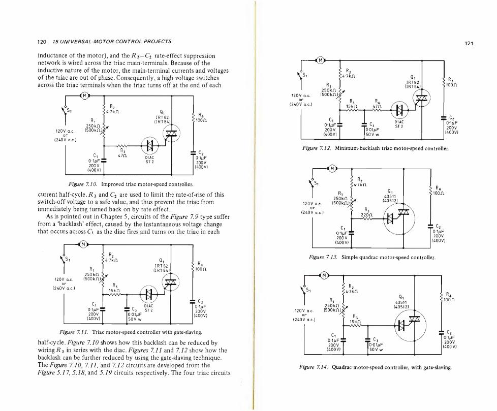
120 15 UNIVERSAL-MOTOR CONTROL PROJECTS
inductance of thè motor), and thè R3-C2 rate-effect suppression network is wired across thè triac main-terminals. Because of thè inductive nature of thè motor, thè main-terminal currents and voltages of thè triac are out of phase. Consequently, a high voltage switches across thè triac terminals when thè triac turns off at thè end of each
Figure 7.10. Improved triac motor-speed controller.
current half-cycle.7?3 and C2 are used to limit thè rate-of-rise of this switch-off voltage to a safe value, and thus prevent thè triac from immediately being turned back on by rate effect.
As is pointed out in Chapter 5, circuits of thè Figure 7.9 type suffer from a ‘backlash’ effect, caused by thè instantaneous voltage change
that occurs across Ci as thè diac flres and turns on thè triac in each
Figure 7.11. Triac motor-speed controller with gate-slaving.
half-cycle. Figure 7.10 shows how this backlash can be reduced by
wiring/?3 in series with thè diac. Fìgures 7.11 and 7.12 show how thè backlash can be further reduced by using thè gate-slaving technique.
The Figure 7.10, 7.77, and 7.72 circuits are developed from thè Figure 5.17, 5.18, and 5.19 circuits respectively. The four triac circuits
121
Figure 7.14. Quadrac motor-speed controller, with gate-slaving.
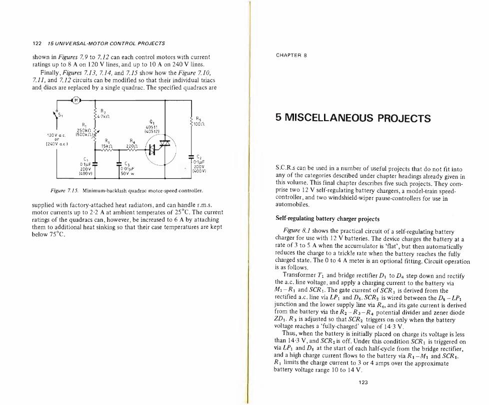
122 15 UNIVERSAL-MOTOR CONTROL PROJECTS
shown in Figures 7.9 to 7.12 can each control motors with current ratings up to 8 A on 120 V lines, and up to 10 A on 240 V lines.
Finally, Figures 7.13, 7.14, and 7.15 show how thè Figure 7.10, 7.77, and 7.12 circuits can be modified so that their individuai triacs and diacs are replaced by a single quadrac. The specified quadracs are
Figure 7.15. Minimum-backlash quadrac motor-speed controller.
supplied with factory-attached heat radiators, and can handle r.m.s. motor currents up to 2*2 A at ambient temperates of 25°C. The current ratings of thè quadracs can, however, be increased to 6 A by attaching them to additional heat sinking so that their case temperatures are kept below 75°C.
CHAPTER 8
5 MISCELLANEOUS PROJECTS
S C.R.s can be used in a number of useful projects that do not fit into any of thè categories described under chapter headings already given in this volume. This final chapter describes flve such projects. They com-
prise two 12 V self-regulating battery chargers, a model-train speed- controller, and two windshield-wiper pause-controllers for use in automobiles.
Self-regulating battery charger projects
Figure 8.1 shows thè practical Circuit of a self-regulating battery charger for use with 12 V batteries. The device charges thè battery at a
rate of 3 to 5 A when thè accumulator is ‘fiat*, but then automatically reduces thè charge to a trickle rate when thè battery reaches thè fully
charged state. The 0 to 4 A meter is an optional fitting. Circuit operation is as follows.
Transformer T\ and bridge rectifìer D\ to Z>4 step down and rectify thè a.c. line voltage, and apply a charging current to thè battery via
M\—Ri andSCRi. The gate current of SCRi is derived from thè rectified a.c. line via LPi and Ds. SCR2 is wired between thè Ds -LP\ junction and thè lower supply line via R6, and its gate current is derived from thè battery via theR2 -R3-R4 potential divider and zener diode ZD1. 7? 3 is adjusted so that SCR2 triggers on only when thè battery voltage reaches a ‘fully-charged’ value of 14-3 V.
Thus, when thè battery is initially placed on charge its voltage is less than 14*3 V, and SCR2is off. Under this conditionSCRi is triggered on via LP1 and D5 at thè start of each half-cycle from thè bridge rectifìer, and a high charge current flows to thè battery via Ri -Mi and SCRi. Ri limits thè charge current to 3 or 4 amps over thè approximate battery voltage range 10 to 14 V.
123
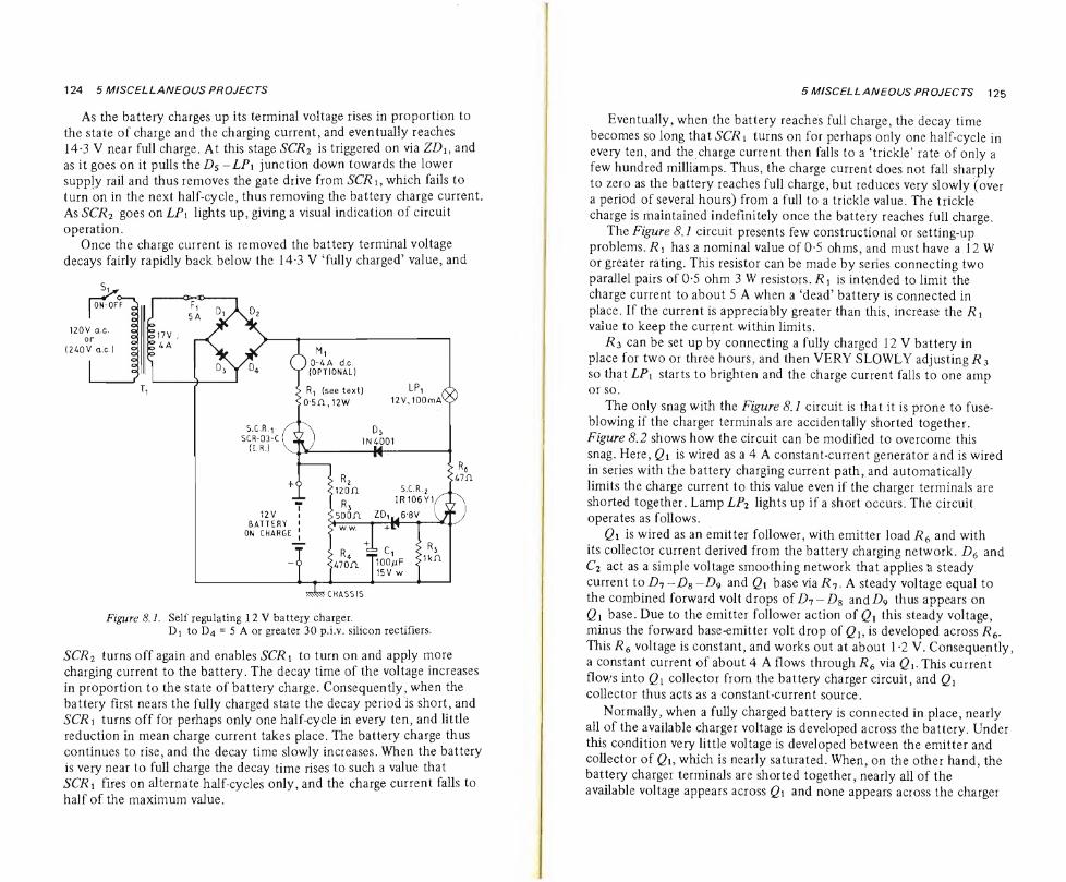
124 5 MtSCELLANEOUS PROJECTS
As thè battery charges up its terminal voltage rises in proportion to thè state of charge and thè charging current, and eventually reaches 14*3 V near full charge. At this stage SCR2 is triggered on via ZDU and as it goes on it pulls thè Ds —LP\ junction down towards thè lower supply rail and thus removes thè gate drive from SCR i, which fails to turn on in thè next half-cycle, thus removing thè battery charge current. As SCR2 goes on LP\ lights up, giving a visual indication of Circuit
operation. Once thè charge current is removed thè battery terminal voltage
decays fairly rapidly back below thè 14*3 V ‘fully charged’ value, and
Figure 8.1. Self regulating 12 V battery charger. Di to D4 = 5 A or greater 30 p.i.v. Silicon rectifiers.
SCR2 turns off again and enables SCR\ to turn on and apply more charging current to thè battery. The decay time of thè voltage increases
in proportion to thè state of battery charge. Consequently, when thè battery fìrst nears thè fully charged state thè decay period is short, and SCR\ turns off for perhaps only one half-cycle in every ten, and little
reduction in mean charge current takes place. The battery charge thus continues to rise, and thè decay time slowly increases. When thè battery is very near to full charge thè decay time rises to such a value that SCR\ fìres on alternate half-cycles only, and thè charge current falls to half of thè maximum value.
5 MtSCELLANEOUS PROJECTS 125
Eventually, when thè battery reaches full charge, thè decay time becomes so long that SCR\ turns on for perhaps only one half-cycle in every ten, and thè charge current then falls to a ‘trickle’ rate of only a few hundred milliamps. Thus, thè charge current does not fall sharply to zero as thè battery reaches full charge, but reduces very slowly (over a period of several hours) from a full to a trickle value. The trickle charge is maintained indefìnitely once thè battery reaches full charge.
The Figure 8.1 Circuit presents few constructional or setting-up problems./?i has a nominai value of 0*5 ohms, and must have a 12 W or greater rating. This resistor can be made by series connecting two parallel pairs of 0*5 ohm 3 W resistors.Ri is intended to limit thè charge current to about 5 A when a ‘dead’ battery is connected in
place. If thè current is appreciably greater than this, increase thè R i value to keep thè current within limits.
R$ can be set up by connecting a fully charged 12 V battery in place for two or three hours, and then VERY SLOWLY adjustingR3 so that LP\ starts to brighten and thè charge current falls to one amp or so.
The only snag with thè Figure 8.1 Circuit is that it is prone to fuse- blowingif thè charger terminals are accidentally shorted together.
Figure 8.2 shows how thè Circuit can be modifìed to overcome this
snag. Here, Gì is wired as a 4 A constant-current generator and is wired in series with thè battery charging current path, and automatically limits thè charge current to this value even if thè charger terminals are shorted together. Lamp LP2 lights up if a short occurs. The Circuit operates as follows.
Gì is wired as an emitter follower, with emitter load R6 and with its collector current derived from thè battery charging network. D6 and C2 act as a simple voltage smoothing network that applies a steady
current toD7-Ds-D9 and Gì base viaR7. A steady voltage equal to thè combined forward volt drops of D7-Z)8 andD9 thus appears on Gì base. Due to thè emitter follower action of Q1 this steady voltage, minus thè forward base-emitter volt drop of Gì, is developed across R6. This R6 voltage is Constant, and works out at about 1 *2 V. Consequently, a Constant current of about 4 A flows through R6 via Gì* This current flov/s into Gì collector from thè battery charger Circuit, and Gì collector thus acts as a constant-current source.
Normally, when a fully charged battery is connected in place, nearly all of thè available charger voltage is developed across thè battery. Under this condition very little voltage is developed between thè emitter and collector of Gì, which is nearly saturated. When, on thè other hand, thè battery charger terminals are shorted together, nearly all of thè available voltage appears across Gì and none appears across thè charger
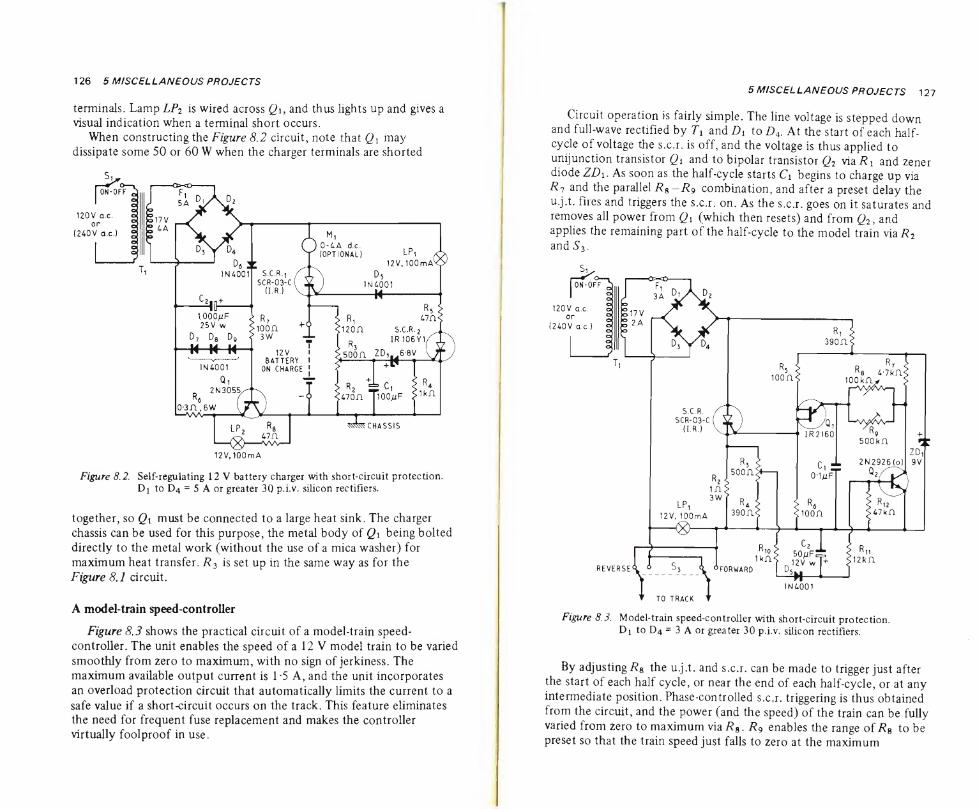
126 5 MtSCELLANEOUS PROJECTS
terminals. Lamp LP2 is wired across Q\y and thus lights up and gives a visual indication when a terminal short occurs.
When constructing thè Figure 8.2 Circuit, note that Qx may dissipate some 50 or 60 W when thè charger terminals are shorted
Figure 8.2. Self-regulating 12 V battery charger with short-circuit protection. Di to D4 = 5 A or greater 30 p.i.v. Silicon rectiflers.
together, so Q\ must be connected to a large heat sink. The charger chassis can be used for this purpose, thè metal body of Qi being bolted
directly to thè metal work (without thè use of a mica washer) for maximum heat transfer. R3 is set up in thè same way as for thè Figure 8.1 circuit.
A model-train speed-controller
Figure 8.3 shows thè practical circuit of a model-train speed- controller. The unit enables thè speed of a 12 V model train to be varied
smoothly from zero to maximum, with no sign of jerkiness. The maximum available output current is 1*5 A, and thè unit incorporates an overload protection circuit that automatically limits thè current to a
safe value if a short-circuit occurs on thè track. This feature eliminates thè need for frequent fuse replacement and makes thè controller virtually foolproof in use.
5 MfSCELLANEOUS PROJECTS 127
Circuit operation is fairly simple. The line voltage is stepped down and full-wave rectified by 7\ and Dx to Z)4. At thè start of each half- cycle of voltage thè s.c.r. is off, and thè voltage is thus applied to unijunction transistor Qi and to bipolar transistor Q2 via Ri and zener diode ZDi. As soon as thè half-cycle starts Cx begins to charge up via R-j and thè parallel R$— R9 combination, and after a preset delay thè u.j.t. fiies and triggers thè s.c.r. on. As thè s.c.r. goes on it saturates and removes all power from Qx (which then resets) and from Q2, and applies thè remaining part of thè half-cycle to thè model train v[aR2
and S3.
Figure 8.3. Model-train speed-controller with short-circuit protection. Di to D4 = 3 A or greater 30 p.i.v. Silicon rectiflers.
By adjusting/?e thè u.j.t. and s.c.r. can be made to trigger just after thè start of each half cycle, or near thè end of each half-cycle, or at any
intermediate position. Phase-controlled s.c.r. triggering is thus obtained from thè circuit, and thè power (and thè speed) of thè train can be fully varied from zero to maximum via R&. R9 enables thè range of Rg to be preset so that thè train speed just falls to zero at thè maximum
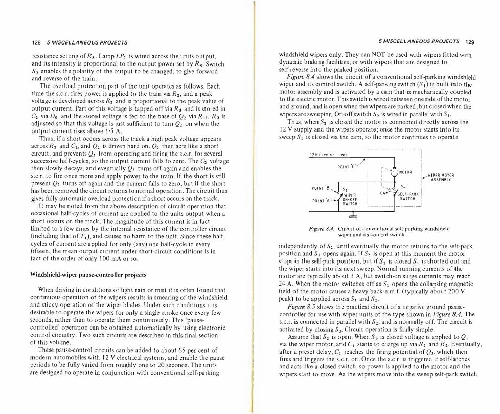
128 5 M/SCELLANEOUS PROJECTS
resistance setting of R%. Lamp LP\ is wired across thè units output, and its intensity is proportional to thè output power set by R$. Switch S3 enables thè polarity of thè output to be changed, to give forward and reverse of thè train.
The overload protection part of thè unit operates as follows. Each time thè s.c.r. fires power is applied to thè train via R2, and a peak voltage is developed across R2 and is proportional to thè peak value of output current. Part of this voltage is tapped off via R3 and is stored in C2 via Ds, and thè stored voltage is fed to thè base of Q2 viaRn. R3 is adjusted so that this voltage is just suffìcient to turn Q2 on when thè output current rises above 1*5 A.
Thus, if a short occurs across thè track a high peak voltage appears across R2 and C2, and Q2 is driven hard on. Q2 then acts like a short Circuit, and prevents Q\ from operating and fìring thè s.c.r. for several successive half-cycles, so thè output current falls to zero. The C2 voltage then slowly decays, and eventually Q2 turns off again and enables thè s.c.r. to fìre once more and apply power to thè train. If thè short is stili present Q2 turns off again and thè current falls to zero, but if thè short
has been removed thè Circuit returns tonormal operation. The Circuit thus gives fully automatic overload protection if a short occurs on thè track.
It may be noted from thè above description of Circuit operation that occasionai half-cycles of current are applied to thè units output when a short occurs on thè track. The magnitude of this current is in fact
limited to a few amps by thè internai resistance of thè controller circuit
(including that of 7\), and causes no harm to thè unit. Since these half- cycles of current are applied for only (say) one half-cycle in every fìfteen, thè mean output current under short-circuit conditions is in fact of thè order of only 100 mA or so.
Windshield-wiper pause-controller projects
When driving in conditions of light rain or mist it is often found that continuous operation of thè wipers results in smearing of thè windshield and sticky operation of thè wiper blades. Under such conditions it is
desirable to operate thè wipers for only a single stroke!once every few
seconds, rather than to operate them continuously. This ‘pause-
controlled’ operation can be obtained automatically by using electronic control circuitry. Two such circuits are described in this final section of this volume.
These pause-control circuits can be added to about 65 per cent of modern automobiles with 12 V electrical systems, and enable thè pause periods to be fully varied from roughly one to 20 seconds. The units are designed to operate in conjunction with conventional self-parking
5 M/SCELLANEOUS PROJECTS 129
windshield wipers only. They can NOT be used with wipers fitted with dynamic braking facilities, or with wipers that are designed to self-reverse into thè parked position.
Figure 8.4 shows thè circuit of a conventional self-parking windshield wiper and its control switch. A self-parking switch (Si) is built into thè motor assembly and is activated by a cam that is mechanically coupled to thè electric motor. This switch is wired between one side of thè motor and ground, and is open when thè wipers are parked, but closed when thè wipers are sweeping. On-off switch S2 is wired in parallel with Sy.
Thus, when S2 is closed thè motor is connected directly across thè 12 V supply and thè wipers operate; once thè motor starts into its sweep Si is closed via thè cam, so thè motor contìnues to operate
WIPER MOTOR ASSEMBIY
Figure iSA. Circuit of conventional self-parking windshield wiper and its control switch.
independently of S2ì until eventually thè motor returns to thè self-park position and Si opens again. If S2 is open at this moment thè motor stops in thè self-park position, but if S2 is closed Si is shorted out and thè wiper starts into its next sweep. Normal running currents of thè motor are typically about 3 A, but switch-on surge currents may reach 24 A. When thè motor switches off as Si opens thè collapsing magnetic
fìeld of thè motor causes a heavy back-e.m.f. (typically about 200 V peak) to be applied across Si and S2.
Figure 8.5 shows thè practical circuit of a negative ground pause- controller for use with wiper units of thè type shown in Figure 8.4. The s.c.r. is connected in parallel with S2, and is normally off. The circuit is activated by closingS3. Circuit operation is fairly simple.
Assume that S2 is open. When S3 is closed voltage is applied to Qi via thè wiper motor, and Cx starts to charge up via R\ and R2. Eventually, after a preset delay, Cy reaches thè fìring potentialof Qi, which then fires and triggers thè s.c.r. on. Once thè s.c.r. is triggered it self-latches and acts like a closed switch, so power is applied to thè motor and thè wipers start to move. As thè wipers move into thè sweep self-park switch

130 5 MfSCELLANEOUS PROJECTS
Si closes and shorts out thè s.c.r. and Ql Circuit, which turn off and reset, and thè motor completes thè sweep via Si. At thè end of thè sweep Si again opens, so Q\ starts into another timing cycle, at thè end of which it again fires thè s.c.r. and restarts thè wipers. This process continues so long as £3 is closed. When S$ is opened power is no longer applied to Q\ at thè end of each sweep, so Circuit operation ceases.
> Fig. 8.4
Figure 8.5. Windshield-wiper pause-controUer, -ve ground version.
Ri enables thè timing delay periods of thè Circuit to be varied from roughly one to 20 seconds. Di and D2 limit thè switch-off back-e.m.f. of thè motor to about 13 V, thus eliminating thè danger of possible
semiconductor damage at thè moment of switch-off, and C2 limits thè rate-of-rise of thè s.c.r. anode voltage, thus ensuring that thè s.c.r. is not turned on by switching transients.
The positive ground version of thè unit, shown in Figure 8.6, is almost identical to that described above, except that thè Circuit con- nections are changed. In both circuits thè specified s.c.r. has an 8 A average and 80 A surge rating, and thus has ampie safety margins for operating thè wiper motors. The s.c.r. should be mounted on a small heat sink in thè completed circuits, to prevent overheating.
Figure 8.6. Windshield-wiper pause controUer, +ve ground version.
5 MfSCELLANEOUS PROJECTS 131
Before starting construction, make sure that thè wipers are suitable for operation by thè selected pause-controller Circuit. This can be determined very easily, as follows. Gain access to thè vehicle’s wiper control switch terminals via a couple of clip-on wires. Switch on thè ignition, and touch-connect a 5 A to 8 A SLOW-BLOW fuse across thè switch terminals. The wipers should operate in thè normal way. Let thè wipers work through two or three sweeps, and then remove thè fuse half way through a following sweep. The wipers should continue through this sweep and then stop in thè self-park position. If thè wipers work as described, thè electronic unit can safely be used on thè vehicle. If, on thè other hand, thè fuse blows during these tests, or thè wipers fai! to self-park, thè unit can not be used on thè vehicle.
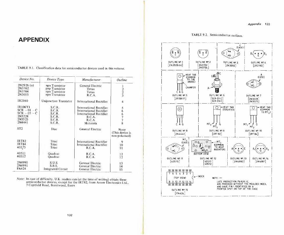
APPENDIX
TABLE 9.1. Classifìcation data for semiconductor devices used in this volume.
Device No. Device Type Manufacturer Ou dine
2N2926 (o) npn Transistor General Electric 1 2N3702 pnp Transistor Texas 2 2N3704 npn Transistor Texas 2 2N3055 npn Transistor R.C.A. 3
IR2160 Unijunction Transistor International Rectifìer 4
IR106Y1 S.C.R. International Rectifìer 5 SCR -01 -C S.C.R. International Rectifìer 6 SCR - 03 - C S.C.R. International Rectifìer 6 2N3228 S.C.R. R.C.A. 7 2N3525 S.C.R. R.C.A. 7 2N4441 S.C.R. Motorola 8
ST2 Diac General Electric None (This device is non-polarised)
IRT82 Triac International Rectifìer 9 IRT84 Triac International Rectifìer 10 40575 Triac R.C.A. 11
40511 Quadrac R.C.A. 12 40512 Quadrac R.C.A. 12
2N4990 S.U.S. General Electric 13 2N4991 S.B.S. General Electric 14 PA424 Integrated Circuit General Electric 15
Note: In case of difficuity, U.K. readers can (at thè time of writing) obtain these semiconductor devices, except for thè IRT82, from Arrow Electronics Ltd., 7 Coptfold Road, Brentwood, Essex
132
Appendix 133
TABLE 9.2. Semiconductor outlines.
OUTLINE N®. 1 [2 N 2926(o)]
OUTLINE N®. 2 f 2N37021 [2N3704-J
OUTLINE N®. 3 [2N3055]
O .HEAT TAB ^
OUTLINE N®. 4
[IR2160]
fih (COMMON TO THE ANODE)
CHAMFER
C AG OUTLINE NP.5
[iR 106 Y l]
' ' I^ucat tao —^— - uriT t»
©
C A G
OUTLINE N®. 8
[2N4441]
OUTLINE N®. 6 OUTLINE H9. 7 f SCR-01-C1 | [2N3228] [sCR-03-cJ L2N3525]
MT,-
0 ♦HEAT TA8 ■ f|C,m ATFFM o
\\ jULM 1 £l/| l
1 MT
( MT,-*' f G
(COMMON TO MT2)
OUTLINE N®. 9
[IRT82]
^MTZ (COMMON TO HEAT RADIATORI
OUTLINE N®. IO [IRT 84]
80TT0M VIEW
OUTLINE N® 11 [40575]
TP TT Tf W TT TT TT 7 6 5 4 3 2 1
OUTLINE N®. 12 [40511] [40512]
OUTLINE N®. 13 [2N4990]
OUTLINE N® 14 [2 N 4991]
(TOP VIEW)
8 9 10 11 12 13 14
OUTLINE N®. 15
I [PA424] |
-INDEX NOTE : —
LATE PRODUCTION PA424 I.C. ARE PRODUCED WITHOUT THE MOULDED INDEX. AND HAVE PIN 1 IDENTIFIED BY A PRINTED SPOT ON TOP OF THE CASE
.

Index
A.C, circuits, 8 half-wave on-off, 8 full-wave control, 9
A.C. lamp flasher projects, 77, 78 automatic, 79
synchronous, 81 A.C. time-delay projects, 62 A.C. power switch
with s.b.s. aided triggering, 24 with transistor-aided d.c. triggering,
25 with u.j.t. triggering, 26
A.C. power switching projects, 23 Alarm projects
burglar, 39 self-latching, 42 tamper-proof, 41
contact-operated, 38 electronic, 28 Tire, 39,52 frost, 52 light-beam, 47
unbeatable, 49 light-operated, 46 non-latching, 7 over-temperature, 52, 53 remote-operated, 39 self-latching, 7 smoke-operated, 50 steam-operated, 44 temperature-operated, 51 under-temperature, 52 water-operated, 44
Automatic integral-cycle control projects, 105
Automatic light-activated a.c. lamp projects, 68
indoor use, 70 outdoor use, 69
Automatic overload-switching projects, 35
Automatic turn-off d.c. switch, 58
Basic a.c. circuits, 8
Basic d.c. circuits, 4 s.c.r., 4
Basic d.c. switch s.c.r., 2 triac, 12
Basic principles s.c.r., 1 triac, 11
Basic theory, s.c.r., 1 Battery-charger projects, self-
regulating, 123 Bistable, s.c.r., 6 Burglar alarm, 39
Cadmium-sulphide photocell, 46 Capacitor turn-off Circuit, 5 Characteristics
s.c.r., 2 universal-motor, 110
Classification data, 132 Contact-operated alarm projects, 38
Data, classification, 132 D.C. circuits, s.c.r., 4 D.C. delayed turn-on projects, 82 D.C. lamp-flasher projects, 74 D.C. light-activated lamp flasher, 75 D.C. on-off circuits, 4
s.c.r., 4 Delay projects, 54
a.c., 62 d.c., 58
Delayed turn-on line switch, 64 Diac, 20
ST2, 86, 119, 132, 133
Electronic alarm projects, 38
Fire alarm, 39, 52 Frost alarm, 52 Full-wave a.c. control Circuit, 9
135

136 INDEX
Full-wave control projects, 119 FulFwave line switch, 11 Full-wave s.c.r, on-off Circuit
with a,c. load, 10 with d.c. load, 10
Gate sensitivity, triac, 12
Half-wave control projects, 111 Half-wave motor-speed controller, 112
with self-regulation, 114 high-performance, 114
with transistor trigger, 113 Half-wave universal-motor control
projects, 110 Heater control projects, 94 Heater controller,
self-regulating, 107 Heater, thermistor-controlled, 95, 97
synchronous, 97, 99, 101 with tri-mode operation, 96
High performance lamp dimmer, 92
Integral-cycle heater controller, self- regulating, 107
Integral-cycle variable power projects, 100
automatic, 105 Interference, radio frequency, 16 IR106Y1, 38, 126 IR2160, 26,54, 127, 132, 133 IRT82, 23,94, 132, 133 IRT84, 23,94, 132, 133 Isolated-input line switch, 27
Lamp-chaser projects d.c., 82 repetitive, 83
Lamp-control projects, 68 time-delayed, 71
Lamp-control unit, 91 Lamp-dimmer projects, 85
high-performance, 92 phase-triggered, 85 simple quadrac, 89 single-lamp, 87 with gate slaving, 88
Lamp-flasher projects a.c., 77
Lamp-flasher projects (contd) automatic, 79
synchronous, 81 d.c., 74 light-activated, 75 twin-lamp d.c., 76
L.A.S.C.R., 18 Light-activated a.c. lamp projects, 68
indoor use, 70 outdoor use, 69
Light-activated alarm, 46 Light-activated s.c.r., 18 Light-beam alarm, 47 Light-dependent resistor, 46 Light-operated alarms, 46 Line-triggered a.c. power switch, 23
MiscelJaneous projects, 123 Miscellaneous thyristor and trigger
devices, 18 Model-train speed-controller, 126 Motor-speed controller, half-wave,
112
high-performance, 114 with self-regulation, 114 with transistor trigger, 113
Motor-speed controller, quadrac, 121 with gate slaving, 121
Motor-speed controller, triac, 119 with gate slaving, 120
On-off circuits automatic overload switch, 35 automatic turn-off, d.c., 58 basic d.c. switch, s.c.r., 2
triac, 12 d.c. triggered line switch, 13 delayed turn-on, 54
line, 64 full-wave line switch, 11 full-wave with d.c. load, 10 half-wave a.c., 8 half-wave line driven, 9 isolated-input line switch, 27 push-button self-latching line
switch, 29 steam-operated, 27, 28 synchronous, 97 water-operated, 27, 28
Oscillator, relaxation, u.j.t., 21 Outlines, 133
INDEX 137
Over-temperature alarm, 52
PA424, 32, 100, 104, 109, 132, 133 Phase-triggered power-control
principles, 15 waveforms, 15
Photocell, cadmium sulphide, 46 Power-control projects, 100
automatic, 105 Power switching, a.c., 23 Precision over-temperature alarm, 53 Push-button operated self-latching line
switch, 29
Quadrac, 20 motor-speed controller, 121
with gate slaving, 121 40511, 89, 121, 122, 132, 133 40512, 89, 121, 122, 132, 133
Radio-frequency interference, 16 Rate effect demonstration Circuit, 8 Relaxation oscillator, 21
waveforms, 22 Remote-operated alarm, 39 Repetitive lamp chaser, 83
S.B.S., 19 symbol, 20 2N4991, 24, 132, 133
S.C.R. basic a.c. circuits, 8 basic d.c. circuits, 4 basic d.c. switch, 2 basic principles and projects, 1 basic theory, 1 bistable, 6 capacitor turn-off Circuit, 5 characteristics, 2 d.c. on-off Circuit, 4 full-wave a.c. control, 9 full-wave line switch, 11 full-wave on-off Circuit with a.c.
load, 10 with d.c. load, 10
half-wave a.c. on-off Circuit, 8 IR106Y1, 4,38,54,124,126,
132,133
S.C.R. (contd) line-driven half-wave on-off
Circuit, 9 non-latching alarm circuit, 7 rate-effect demonstration
circuit, 8 symbol, 2 transistor equivalent, 2 2N3228, 9, 112, 132, 133 2N3525, 9, 112, 132, 133 2N4441, 130, 132, 133 SCR-03-C, 124,126,132,133
S.C.S., 18 symbol, 18
Self-latching alarm circuit, 7 Self-latching burglar alarm, 42 Self-regulating battery-charger
projects, 123 Semiconductor
classification data, 132 outlines, 133
Sensitivity, triac gate, 12 Silicon bilateral switch, 19 Silicon controlled switch, 18
symbol, 18 Silicon unilateral switch, 19
symbol, 19 Simple lamp dimmer, 87 Simple quadrac lamp dimmer, 89 Smoke-operated alarm, 50 Speed-controller, model train, 126 Steam-operated alarms, 44 Steam-operated line switch, 27, 28 S.U.S.
symbol, 19 2N4990, 112, 132, 133
Switch automatic overload, 35 d.c. triggered line, 13 full-wave line, 11 isolated-input line, 27 line-triggered, 13, 14
a.c. power, 33 push-button self-latching line, 29 s.c.r. basic, 2 Silicon bilateral, 19 Silicon controlled, 18 Silicon unilateral, 19 steam-operated, 27, 28 synchronous, 29, 30, 34 three-way line, 14 triac, 12 water-operated, 27, 28

138 iNDEX
Symbols diac, 20 l.a.s.e.r., 18 quadrac, 20 s.b.s., 20 s.c.r., 2 s.c.s., 18 s.u.s., 19 triac, 11 unijunction transistor, 21
Synchronous on-off control projects, 97
Synchronous power-switching projects, 29
zero-switching, 30 using i.c., 34
Synchronous thermostat-controlled heaters, 97
Tamper-proof burglar alami, 41 Tempera ture-opera ted alarms, 51 Thermistor-controlled heater, 95
synchronous, 97, 99, 101 with tri-mode operation, 96
Three-way line switch, 14 Thyristor devices, miscellaneous, 18 Time-delay projects, 54 Time-delayed lamp-control projects,
71 Transistor equivalent of s.c.r., 2 Triac
basic principles and projects, 11 basic switch with d.c. gate dtive,
11 d.c. triggered line switch, 13 gate sensitivity, 12 IRT82, 13,62,94,95,132,133
Triac (contd) IRT84, 13,62,94,95,132,133 line-triggered line switch, 13, 14 motor-speed controller, 119
with gate slaving, 120 phase-triggered power control
principles, 15 symbol, 11 three-way line switch, 14 waveforms, 15 40575, 94,95, 132, 133
Trigger devices, miscellaneous, 18 Twin-lamp d.c. flasher, 76
Unbeatable light-beam alarm, 49 Under-temperature alarm, 52 Unijunction transistor, 21
1R2160, 26,54,127,132,133 Simple relaxation oscillator, 21
waveforms, 22 symbol, 21
Universal-motor characteristics, 110 Universal-motor control projects, 110
half-wave, 111
Water-opera ted alarms, 44 Water or steam-operated line switch,
27, 28 Windshield wiper pause controller
projects, 128
Zero-switching synchronous overload switch,
self-latching, 36
osmoscienza
20129 MILANO - VIALE DEI MILLE, 4
TELEFONI 73.82.146 • 73.32.104
I
ì
I
!
110 THYRISTOR PROJECTS using SCRs and TRIACS
During recent years there have been many advances in semi¬ conductor design, and devices have been developed that are capable of controlling larger currents than are used with thè normal transistor. Particularly important are semiconductor power switches that can handle currents that previously could only be controlled by relays. Described in this volume are many projects making use of thyristor devices capable of handling mains voltages that can control currents of tens or hundred of amperes. S.C.R.s and triacs can be used in many applications, such as controlling electric lamps, motors, heaters and alarm systems and can be used to replace mechanical switches and relays in many a.c. and d.c. control systems. The projects described, which range from simple electronic alarms to highly sophisticated self-regulating electric-heater power controllers, should be of equa! interest to thè electronics amateur, to thè student of electronics and to thè professional engineer. As in R. M. Marston's previous books, all thè projects are designed round internationaliy available components and all have been fully evaluated by thè author.
Nci^ésfechnicàlBoòki Butterworfhs, Borough Green, Sevenoaks, Kent TN15 8PH
0 TH
YR
IST
OR
PR
OJE
CT
S
usin
g s.c
.r.s
and tr
iacs
Marsto
n
110 THYRISTOR PROJECTS using SCRs and TRIACS
i LP1 R5
'RIAC 11
R6!
\ \rla
\ X1-! p "di
SCR1
R.M. Marston
110 THYRISTOR PROJECTS using SCRs and TRIACS
During recent years there have been many advances in semi¬ conductor design, and devices have been developed that are capable of controlling larger currents than are used with thè normal transistor. Particularly important are semiconductor power switches that can handle currents that previously could only be controlled by relays. Described in this volume are many projects making use of thyristor devices capable of handling mains voltages that can control currents of tens or hundred of amperes. S.C.R.s and triacs can be used in many applications, such as controlling electric lamps, motors, heaters and alarm systems and can be used to replace mechanical switches and relays in many a.c. and d.c. control systems. The projects described, which range from simple electronic alarms to highly sophisticated self-regulating electric-heater power controllers, should be of equal interest to thè electronics amateur, to thè student of electronics and to thè professional engineer. As in R. M. Marston's previous books, all thè projects are designed round internationaliy available components and all have been fully evaluated by thè author.
Butterworfhs, Borough Green, Sevenoaks, Kent TN15 8PH