
1050fb
16
1 LTC1050 1050fb – + 7 8 13 14 16 17 11 4 1/2 LTC1043 5V C S 1μF C H 1μF DIFFERENTIAL INPUT 12 0.01μF R1 CMRR > 120dB AT DC CMRR > 120dB AT 60Hz DUAL SUPPLY OR SINGLE 5V GAIN = 1 + R2/R1 V OS = 5μV COMMON MODE INPUT VOLTAGE EQUALS THE SUPPLIES R2 1050 TA01 –5V 1μF –5V 5V 4 7 3 2 6 V OUT LTC1050 Precision Zero-Drift Operational Amplifier with Internal Capacitors ■ No External Components Required ■ Noise Tested and Guaranteed ■ Low Aliasing Errors ■ Maximum Offset Voltage: 5μ V ■ Maximum Offset Voltage Drift: 0.05μ V/°C ■ Low Noise: 1.6μ V P-P (0.1Hz to 10Hz) ■ Minimum Voltage Gain: 130dB ■ Minimum PSRR: 125dB ■ Minimum CMRR: 120dB ■ Low Supply Current: 1mA ■ Single Supply Operation: 4.75V to 16V ■ Input Common Mode Range Includes Ground ■ Output Swings to Ground ■ Typical Overload Recovery Time: 3ms The LTC ® 1050 is a high performance, low cost zero-drift operational amplifier. The unique achievement of the LTC1050 is that it integrates on-chip the two sample-and- hold capacitors usually required externally by other chop- per amplifiers. Further, the LTC1050 offers better com- bined overall DC and AC performance than is available from other chopper stabilized amplifiers with or without internal sample-and-hold capacitors. The LTC1050 has an offset voltage of 0.5μ V, drift of 0.01μ V/°C, DC to 10Hz, input noise voltage of 1.6μ V P-P and a typical voltage gain of 160dB. The slew rate of 4V/μ s and a gain bandwidth product of 2.5MHz are achieved with only 1mA of supply current. Overload recovery times from positive and negative satu- ration conditions are 1.5ms and 3ms respectively, which represents an improvement of about 100 times over chop- per amplifiers using external capacitors. Pin 5 is an optional external clock input, useful for synchronization purposes. The LTC1050 is available in standard 8-pin metal can, plastic and ceramic dual-in-line packages as well as an SO-8 package. The LTC1050 can be an improved plug-in replacement for most standard op amps. ■ Thermocouple Amplifiers ■ Electronic Scales ■ Medical Instrumentation ■ Strain Gauge Amplifiers ■ High Resolution Data Acquisition ■ DC Accurate RC Active Filters High Performance, Low Cost Instrumentation Amplifier Noise Spectrum FEATURES DESCRIPTIO U APPLICATIO S U TYPICAL APPLICATIO U FREQUENCY (Hz) 40 VOLTAGE NOISE DENSITY (nV/√Hz) 80 100 140 160 10 1k 10k 100k 1050 TA02 0 100 120 60 20 , LTC and LT are registered trademarks of Linear Technology Corporation.
-
Upload
alex-alexandru -
Category
Documents
-
view
213 -
download
0
Transcript of 1050fb

1
LTC1050
1050fb
–
+7 8
13 14
16 17
11
4
1/2 LTC1043
5V
CS1µF
CH1µF
DIFFERENTIALINPUT
12
0.01µF
R1
CMRR > 120dB AT DCCMRR > 120dB AT 60HzDUAL SUPPLY OR SINGLE 5VGAIN = 1 + R2/R1VOS = 5µVCOMMON MODE INPUT VOLTAGE EQUALS THE SUPPLIES
R2
1050 TA01
–5V
1µF–5V
5V
4
73
2
6VOUTLTC1050
Precision Zero-DriftOperational Amplifier
with Internal Capacitors
No External Components Required Noise Tested and Guaranteed Low Aliasing Errors Maximum Offset Voltage: 5µV Maximum Offset Voltage Drift: 0.05µV/°C Low Noise: 1.6µVP-P (0.1Hz to 10Hz) Minimum Voltage Gain: 130dB Minimum PSRR: 125dB Minimum CMRR: 120dB Low Supply Current: 1mA Single Supply Operation: 4.75V to 16V Input Common Mode Range Includes Ground Output Swings to Ground Typical Overload Recovery Time: 3ms
The LTC®1050 is a high performance, low cost zero-driftoperational amplifier. The unique achievement of theLTC1050 is that it integrates on-chip the two sample-and-hold capacitors usually required externally by other chop-per amplifiers. Further, the LTC1050 offers better com-bined overall DC and AC performance than is availablefrom other chopper stabilized amplifiers with or withoutinternal sample-and-hold capacitors.
The LTC1050 has an offset voltage of 0.5µV, drift of0.01µV/°C, DC to 10Hz, input noise voltage of 1.6µVP-Pand a typical voltage gain of 160dB. The slew rate of 4V/µsand a gain bandwidth product of 2.5MHz are achieved withonly 1mA of supply current.
Overload recovery times from positive and negative satu-ration conditions are 1.5ms and 3ms respectively, whichrepresents an improvement of about 100 times over chop-per amplifiers using external capacitors. Pin 5 is an optionalexternal clock input, useful for synchronization purposes.
The LTC1050 is available in standard 8-pin metal can,plastic and ceramic dual-in-line packages as well as anSO-8 package. The LTC1050 can be an improved plug-inreplacement for most standard op amps.
Thermocouple Amplifiers Electronic Scales Medical Instrumentation Strain Gauge Amplifiers High Resolution Data Acquisition DC Accurate RC Active Filters
High Performance, Low Cost Instrumentation Amplifier Noise Spectrum
FEATURES DESCRIPTIO
U
APPLICATIO SU
TYPICAL APPLICATIO
U
FREQUENCY (Hz)
40
VOLT
AGE
NOIS
E DE
NSIT
Y (n
V/√H
z)
80
100
140
160
10 1k 10k 100k
1050 TA02
0100
120
60
20
, LTC and LT are registered trademarks of Linear Technology Corporation.

2
LTC1050
1050fb
ORDER PARTNUMBER
A
U
G
W
A
W
U
W
ARBSOLUTE XI TI SOperating Temperature Range
LTC1050AC/C .................................. –40°C to 85°CLTC1050H ..................................... – 40°C to 125°CLTC1050AM/M (OBSOLETE) .......... –55°C to 125°C
Total Supply Voltage (V+ to V–) .............................. 18VInput Voltage ........................ (V+ + 0.3V) to (V– – 0.3V)Output Short-Circuit Duration ......................... IndefiniteStorage Temperature Range ................ –65°C to 150°CLead Temperature (Soldering, 10 sec)................. 300°C
WU U
PACKAGE/ORDER I FOR ATIO
LTC1050ACHLTC1050CHLTC1050AMHLTC1050MH
ORDER PARTNUMBER
10501050HTJMAX = 150°C
(Note 1)
TOP VIEW
V+ (CASE)
NC
NC
–IN OUT
EXT CLOCKINPUT
+IN
V –
87
6
53
2
1
4
H PACKAGE8-LEAD TO-5 METAL CAN
S8 PART MARKING
LTC1050CS8LTC1050HS8
1
2
3
4
8
7
6
5
TOP VIEW
NC
V+
OUT
EXT CLOCKINPUT
NC
–IN
+IN
V–
S8 PACKAGE8-LEAD PLASTIC SO
–
+
TJMAX = 150°C, θJA = 150°C/W
1
2
3
4
8
7
6
5
TOP VIEW
NC
–IN
+IN
V–
NC
V+
OUT
EXT CLOCKINPUT
N8 PACKAGE8-LEAD PDIP
1
2
3
4
5
6
7
TOP VIEW
N PACKAGE14-LEAD PDIP
14
13
12
11
10
9
8
NC
NC
NC
–IN
+IN
NC
V –
NC
NC
NC
V+
OUT
NC
NC
TJMAX = 150°C, θJA = 70°C/W
TJMAX = 150°C, θJA = 100°C/W
ORDER PARTNUMBER
LTC1050ACN8LTC1050CN8
ORDER PARTNUMBER
LTC1050CN
Consult LTC Marketing for parts specified with wider operating temperature ranges.
J8 PACKAGE 8-LEAD CERDIPTJMAX = 150°C, θJA = 100°C/W
LTC1050ACJ8LTC1050CJ8LTC1050AMJ8LTC1050MJ8
OBSOLETE PACKAGE
OBSOLETE PACKAGE
ELECTRICAL C CHARA TERISTICSLTC1050AM LTC1050AC
PARAMETER CONDITIONS MIN TYP MAX MIN TYP MAX UNITSInput Offset Voltage (Note 3) ±0.5 ±5 ±0.5 ±5 µVAverage Input Offset Drift (Note 3) ±0.01 ±0.05 ±0.01 ±0.05 µV/°CLong Term Offset Voltage Drift 50 50 nV/√MoInput Offset Current (Note 5) ±20 ±60 ±20 ±60 pA
±300 ±150 pAInput Bias Current (Note 5) ±10 ±30 ±10 ±30 pA
±2000 ±100 pAInput Noise Voltage 0.1Hz to 10Hz (Note 6) 1.6 2.1 1.6 2.1 µVP-P
DC to 1Hz 0.6 0.6 µVP-P
The denotes specifications which apply over the full operating temperaturerange, otherwise specifications are at TA = 25°C. VS = ±5V
Consider the N8 Package for Alternate Source

3
LTC1050
1050fb
ELECTRICAL C CHARA TERISTICSLTC1050AM LTC1050AC
PARAMETER CONDITIONS MIN TYP MAX MIN TYP MAX UNITSInput Noise Current f = 10Hz (Note 4) 1.8 1.8 fA/√HzCommon Mode Rejection Ratio VCM = V– to 2.7V 114 140 114 140 dB
110 110 dBPower Supply Rejection Ratio VS = ±2.375V to ±8V 125 140 125 140 dBLarge-Signal Voltage Gain RL = 10k, VOUT = ±4V 130 160 130 160 dBMaximum Output Voltage Swing RL = 10k ±4.7 ±4.85 ±4.7 ±4.85 V
RL = 100k ±4.95 ±4.95 VSlew Rate RL = 10k, CL = 50pF 4 4 V/µsGain Bandwidth Product 2.5 2.5 MHzSupply Current No Load 1 1.5 1 1.5 mA
2.3 2.3 mAInternal Sampling Frequency 2.5 2.5 kHz
The denotes specifications which apply over the full operating temperaturerange, otherwise specifications are at TA = 25°C. VS = ±5V
The denotes specifications which apply over the full operating temperature range, otherwise specifications are at TA = 25°C.VS = ±5V
LTC1050M/H LTC1050CPARAMETER CONDITIONS MIN TYP MAX MIN TYP MAX UNITSInput Offset Voltage (Note 3) ±0.5 ±5 ±0.5 ±5 µVAverage Input Offset Drift (Note 3) ±0.01 ±0.05 ±0.01 ±0.05 µV/°CLong Term Offset Voltage Drift 50 50 nV/√MoInput Offset Current (Note 5) ±20 ±100 ±20 ±125 pA
±300 ±200 pAInput Bias Current (Note 5) ±10 ±50 ±10 ±75 pA
±2000 ±150 pAInput Noise Voltage RS = 100Ω, 0.1Hz to 10Hz (Note 6) 1.6 1.6 µVP-P
RS = 100Ω, DC to 1Hz 0.6 0.6 µVP-P
Input Noise Current f = 10Hz (Note 4) 1.8 1.8 fA/√HzCommon Mode Rejection Ratio VCM = V– to 2.7V 114 130 114 130 dB
LTC1050M/C 110 110 dBLTC1050H 100 dB
Power Supply Rejection Ratio VS = ±2.375V to ±8V, LTC1050M/C 120 140 120 140 dBLTC1050H 110 dB
Large-Signal Voltage Gain RL = 10k, VOUT = ±4V 120 160 120 160 dBMaximum Output Voltage Swing RL = 10k ±4.7 ±4.85 ±4.7 ±4.85 V
RL = 100k ±4.95 ±4.95 VSlew Rate RL = 10k, CL = 50pF 4 4 V/µsGain Bandwidth Product 2.5 2.5 MHzSupply Current No Load 1 1.5 1 1.5 mA
2.3 2.3 mAInternal Sampling Frequency 2.5 2.5 kHz
Note 1: Absolute Maximum Ratings are those values beyond which the lifeof the device may be impaired.Note 2: Connecting any terminal to voltages greater than V+ or less thanV– may cause destructive latchup. It is recommended that no sourcesoperating from external supplies be applied prior to power-up of theLTC1050.Note 3: These parameters are guaranteed by design. Thermocouple effectspreclude measurement of these voltage levels in high speed automatic testsystems. VOS is measured to a limit determined by test equipmentcapability.
Note 4: Current Noise is calculated from the formula: In = √(2q • Ib)where q = 1.6 • 10–19 Coulomb.Note 5: At TA ≤ 0°C these parameters are guaranteed by design and nottested.Note 6: Every lot of LTC1050AM and LTC1050AC is 100% tested forBroadband Noise at 1kHz and sample tested for Input Noise Voltage at0.1Hz to 10Hz.

4
LTC1050
1050fb
C CHARA TERISTICS
UW
ATYPICAL PERFOR CE
Offset Voltagevs Sampling Frequency
10HzP-P Noisevs Sampling Frequency
Common Mode Input Rangevs Supply Voltage
Supply Current vs TemperatureSupply Current vs Supply VoltageShort-Circuit Output Currentvs Supply Voltage
SAMPLING FREQUENCY, fS (kHz)2.0
OFFS
ET V
OLTA
GE (µ
V)
6
8
10
4.0
1050 G01
4
2
02.5 3.0 3.5 4.5
VS = ±5V
SAMPLING FREQUENCY, fS (Hz)100
0
10Hz
PEA
K-TO
-PEA
K NO
ISE
(µV)
2
4
8
1k 10k
1050 G02
6
1
3
7
5
VS = ±5V
SUPPLY VOLTAGE (V)0
COM
MON
MOD
E RA
NGE
(V)
0
4
±8
1050 G03
–4
–8±2 ±4 ±6±1 ±3 ±5 ±7
8
–2
2
–6
6VCM = V –
Sampling Frequencyvs Supply Voltage
Sampling Frequencyvs Temperature Overload Recovery
TOTAL SUPPLY VOLTAGE, V+ TO V – (V)4
1.5
SAM
PLIN
G FR
EQUE
NCY,
f S (k
Hz)
2.0
2.5
3.0
3.5
6 8 10 12
1050 G04
14 16
TA = 25°C
AMBIENT TEMPERATURE, TA (°C)–50
0
SAM
PLIN
G FR
EQUE
NCY,
f S (k
Hz)
2
5
0 50 75
1050 G05
1
4
3
–25 25 100 125
VS = ±5V
TOTAL SUPPLY VOLTAGE, V + TO V – (V)4
0
SUPP
LY C
URRE
NT, I
S (m
A)
0.25
0.50
0.75
1.00
1.50
6 8 10 12
1050 G07
14 16
1.25
TA = 25°C
AMBIENT TEMPERATURE, TA (°C)–50
0
SUPP
LY C
URRE
NT, I
S (m
A)
0.2
0.6
0.8
1.0
2.0
1.4
0 50 75
1050 G08
0.4
1.6
1.8
1.2
–25 25 100 125
VS = ±5V
TOTAL SUPPLY VOLTAGE, V + TO V – (V)4
–30SHOR
T-CI
RCUI
T OU
TPUT
CUR
RENT
, IOU
T (m
A)
–20
–10
0
2
6
6 8 10 12
1050 G09
14 16
4ISOURCE
VOUT = V –
ISINKVOUT = V +
200mV
0V
0V
–5V
INPUT
OUTPUT
AV = –100 0.5ms/DIVVS = ±5V
1050 G6

5
LTC1050
1050fb
C CHARA TERISTICS
UW
ATYPICAL PERFOR CE
Gain/Phase vs Frequency
FREQUENCY (Hz)
0
VOLT
AGE
GAIN
(dB)
PHASE SHIFT (DEGREES)
20
60
100
120
100 10k 100k 10M
1050 G10
–20
1k 1M
80
40
–40
180
160
120
80
60
200
100
140
220
PHASE
GAIN
VS = ±5VTA = 25°CCL = 100pFRL ≥ 1k
Small-Signal Transient Response Large-Signal Transient Response
LTC1050 DC to 1Hz Noise
0.5µV
10 SEC1050 G13
LTC1050 DC to 10Hz Noise
1µV
1 SEC1050 G14
100mVSTEP
AV = 1RL = 10kCL = 100pFVS = ±5V
1050 G11
2V
AV = 1RL = 10kCL = 100pFVS = ±5V
1050 G12
VOUT
VIN = 6V
6
LTC1050
1050fb
U
SA
O
PPLICATI
WU U
I FOR ATIOACHIEVING PICOAMPERE/MICROVOLTPERFORMANCE
Picoamperes
In order to realize the picoampere level of accuracy of theLTC1050, proper care must be exercised. Leakage currentsin circuitry external to the amplifier can significantly degradeperformance. High quality insulation should be used (e.g.,Teflon, Kel-F); cleaning of all insulating surfaces to removefluxes and other residues will probably be necessary—particularly for high temperature performance. Surfacecoating may be necessary to provide a moisture barrier inhigh humidity environments.
Board leakage can be minimized by encircling the inputconnections with a guard ring operated at a potential closeto that of the inputs: in inverting configurations the guardring should be tied to ground; in noninverting connectionsto the inverting input (see Figure 1). Guarding both sidesof the printed circuit board is required. Bulk leakage reduc-tion depends on the guard ring width.
Microvolts
Thermocouple effect must be considered if the LTC1050’sultralow drift is to be fully utilized. Any connection of dis-similar metals forms a thermoelectric junction producingan electric potential which varies with temperature (Seebeckeffect). As temperature sensors, thermocouples exploit thisphenomenon to produce useful information. In low driftamplifier circuits the effect is a primary source of error.
Connectors, switches, relay contacts, sockets, resistors,solder and even copper wire are all candidates for thermal
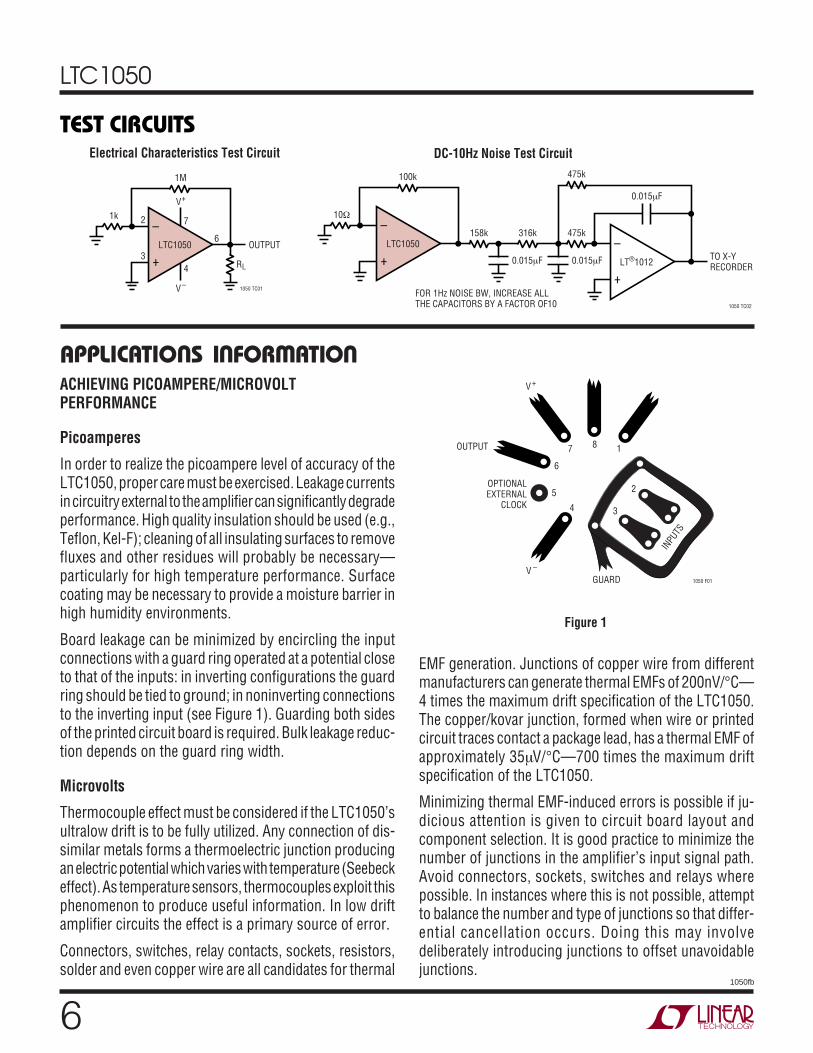
TEST CIRCUITS
–
+LTC1050 OUTPUT
1050 TC01
V+
1k
1M
6
72
34 RL
V –
–
+LTC1050 –
+LT®1012
1050 TC02
10Ω
100k
158k 316k 475k
475k
0.015µF
FOR 1Hz NOISE BW, INCREASE ALL THE CAPACITORS BY A FACTOR OF10
0.015µF
0.015µF
TO X-YRECORDER
Electrical Characteristics Test Circuit DC-10Hz Noise Test Circuit
EMF generation. Junctions of copper wire from differentmanufacturers can generate thermal EMFs of 200nV/°C—4 times the maximum drift specification of the LTC1050.The copper/kovar junction, formed when wire or printedcircuit traces contact a package lead, has a thermal EMF ofapproximately 35µV/°C—700 times the maximum driftspecification of the LTC1050.
Minimizing thermal EMF-induced errors is possible if ju-dicious attention is given to circuit board layout andcomponent selection. It is good practice to minimize thenumber of junctions in the amplifier’s input signal path.Avoid connectors, sockets, switches and relays wherepossible. In instances where this is not possible, attemptto balance the number and type of junctions so that differ-ential cancellation occurs. Doing this may involvedeliberately introducing junctions to offset unavoidablejunctions.
8 17
V +
V –
6
OUTPUT
1050 F01
5OPTIONALEXTERNAL
CLOCK 4
GUARD
2
3
INPU
TS
Figure 1

7
LTC1050
1050fb
Figure 2 is an example of the introduction of an unneces-sary resistor to promote differential thermal balance.Maintaining compensating junctions in close physical prox-imity will keep them at the same temperature and reducethermal EMF errors.
U
SA
O
PPLICATI
WU U
I FOR ATIOPACKAGE-INDUCED OFFSET VOLTAGE
Package-induced thermal EMF effects are another impor-tant source of errors. It arises at the copper/kovar junctionsformed when wire or printed circuit traces contact apackage lead. Like all the previously mentioned thermalEMF effects, it is outside the LTC1050’s offset nulling loopand cannot be cancelled. The input offset voltage specifi-cation of the LTC1050 is actually set by the package-inducedwarm-up drift rather than by the circuit itself. The thermaltime constant ranges from 0.5 to 3 minutes, dependingupon package type.
OPTIONAL EXTERNAL CLOCK
An external clock is not required for the LTC1050 tooperate. The internal clock circuit of the LTC1050 sets thenominal sampling frequency at around 2.5kHz. This fre-quency is chosen such that it is high enough to remove theamplifier 1/f noise, yet still low enough to allow internalcircuits to settle.The oscillator of the internal clock circuithas a frequency 4 times the sampling frequency and itsoutput is brought out to Pin 5 through a 2k resistor. Whenthe LTC1050 operates without using an external clock,Pin 5 should be left floating and capacitive loading on thispin should be avoided. If the oscillator signal on Pin 5 isused to drive other external circuits, a buffer with lowinput capacitance is required to minimize loading on thispin. Figure 3 illustrates the internal sampling frequencyversus capacitive loading at Pin 5.
–
+LTC1050 OUTPUT
1050 F02
NOMINALLYUNNECESSARY
RESISTOR USED TOTHERMALLY BALANCE
OTHER INPUT RESISTOR
RESISTOR LEAD, SOLDERCOPPER TRACE JUNCTION
LEAD WIRE/SOLDER/COPPERTRACE JUNCTION
Figure 2
When connectors, switches, relays and/or sockets arenecessary they should be selected for low thermal EMFactivity. The same techniques of thermally balancing andcoupling the matching junctions are effective in reducingthe thermal EMF errors of these components.
Resistors are another source of thermal EMF errors.Table 1 shows the thermal EMF generated for differentresistors. The temperature gradient across the resistor isimportant, not the ambient temperature. There are twojunctions formed at each end of the resistor and if thesejunctions are at the same temperature, their thermalEMFs will cancel each other. The thermal EMF numbersare approximate and vary with resistor value. High valuesgive higher thermal EMF.Table 1. Resistor Thermal EMFRESISTOR TYPE THERMAL EMF/°C GRADIENT
Tin Oxide ~mV/°C
Carbon Composition ~450µV/°C
Metal Film ~20µV/°C
Wire Wound Evenohm ~2µV/°C Manganin ~2µV/°C
CAPACITANCE LOADING (pF)1
1
SAM
PLIN
G FR
EQUE
NCY,
f S (k
Hz)
2
105 100
1050 F03
3VS = ±5V
Figure 3. Sampling Frequency vs Capacitance Loading at Pin 5

8
LTC1050
1050fb
U
SA
O
PPLICATI
WU U
I FOR ATIOWhen an external clock is used, it is directly applied toPin 5. The internal oscillator signal on Pin 5 has very lowdrive capability and can be overdriven by any externalsignal. When the LTC1050 operates on ±5V power sup-plies, the external clock level is TTL compatible.
Using an external clock can affect performance of theLTC1050. Effects of external clock frequency on inputoffset voltage and input noise voltage are shown in theTypical Performance Characteristics section. The sam-pling frequency is the external clock frequency dividedby 4. Input bias currents at temperatures below 100°Care dominated by the charge injection of input switchesand they are basically proportional to the samplingfrequency. At higher temperatures, input bias currentsare mainly due to leakage currents of the input protectiondevices and are insensitive to the sampling frequency.
LOW SUPPLY OPERATION
The minimum supply for proper operation of the LTC1050is typically below 4V (±2V). In single supply applications,
PSRR is guaranteed down to 4.7V (±2.35V) to ensureproper operation down to the minimum TTL specifiedvoltage of 4.75V.
PIN COMPATIBILITY
The LTC1050 is pin compatible with the 8-pin versions of7650, 7652 and other chopper-stabilized amplifiers. The7650 and 7652 require the use of two external capacitorsconnected to Pin 1 and Pin 8 that are not needed for theLTC1050. Pin 1 and Pin 8 of the LTC1050 are not con-nected internally while Pin 5 is an optional external clockinput pin. The LTC1050 can be a direct plug-in for the 7650and 7652 even if the two capacitors are left on the circuitboard.
In applications operating from below 16V total powersupply, (±8V), the LTC1050 can replace many industrystandard operational amplifiers such as the 741, LM101,LM108, OP07, etc. For devices like the 741 and LM101,the removal of any connection to Pin 5 is all that isneeded.
U
SA
O
PPLICATITYPICAL
–
+LTC1050
–5V
5V
–
+LTC1050
7
5V
5V2.5V
–5V
2
34
61N4148
2N2907
–5V
10kZERO R2
0.1%
OUTPUT±2.5V
R10.1%
GAINTRIM
7
4
6
*
C**
1050 TA03
3
2
2k
301kRN60C
120Ω
51Ω2W *
**
OPTIONAL REFERENCE OUT TO MONITORING 10-BIT A/D CONVERTERAT GAIN = 1000, 10Hz PEAK-TO-PEAK NOISE IS <0.5LSB FOR 10-BIT RESOLUTION
LT1009350ΩBRIDGE
Strain Gauge Signal Conditioner with Bridge Excitation

9
LTC1050
1050fb
U
SA
O
PPLICATITYPICAL
Single Supply Thermocouple Amplifier
–
+LTC1050
7
5V
0.068µF
0°C ~ 100°C TEMPERATURE RANGE
100Ω1k1%
2
3
1050 TA04
7
2
4 5
5V
40.1µF
TYPE K
+–
6 VOUT10mV/°C
255k1%
K
LT1025A
GND R–
–
+LTC1050
7
1050 TA06
5V
TYPE K
2
LT1004-1.2
34
100k1%
6 5V = NO AIR FLOW0V = AIR FLOW
1k
AMBIENTTEMPERATURE
STILL AIR
10k
43.2Ω1%
240Ω–
+
–
+
AIR FLOW
Air Flow Detector
–
+LTC1050
7
0.33µF
10µF
0°C ~ 500°C TEMPERATURE RANGE2°C MAX ERROR*THERMOCOUPLE LINEARIZATION CODE AVAILABLE FROM LTC
1k0.1%
62
4
2
3
1050 TA05
8
2
4 5
4 1µF
LTC1092
TO µP*
1µF
TYPE J
+–
6
0.1µF
178k0.1% 1N4148
3.4k1%
47Ω
J
LT1025A
GND R–
VIN
CS
+IN
–IN
GND
VCC
CLK
DOUT
VREF
1
2
3
4
8
7
6
5
LT1021C-5
VIN = 9V
+
Battery-Operated Temperature Monitor with 10-Bit Serial Output A/D

10
LTC1050
1050fb
U
SA
O
PPLICATITYPICAL
Fast Precision Inverter
–
+LTC1050
72
34
FULL POWER BANDWIDTH = 2MHzSLEW RATE ≥ 40V/µsSETTLING TIME = 5µs TO 0.01% (10V STEP)OFFSET VOLTAGE = 5µVOFFSET DRIFT = 50nV/°C
6
5V
100pF10k
INPUT
1000pF
–5V
–
+LT318A
72
34
6 OUTPUT
5V
5pF
–5V
10k
10k1%
10k
1050 TA07
10k
±100mA Output Drive
–
+LTC1050
72
34
–5V
5V
FULL POWER BANDWIDTH = 10kHzVOS = 5µVVOS/∆T = 50nV/°CGAIN = 10
6
100pF5V
–5V
10kVIN
RL
±100mA
1050 TA08
100k
VOUT
LT1010
Ground Referred Precision Current Sources
–
+LTC1050
72
34
+
–
V +
2N2222
LT1034
10k
6RSET
1050 TA09
0 ≤ IOUT ≤ 25mA*0.2V ≤ VOUT ≤ (V +) – 2V*MAXIMUM CURRENT LIMITED BY POWER DISSIPATION OF 2N2222
1.235VRSET
IOUT =
VOUT
–
+LTC1050
73
24
+
–
V – LT1034
2N2907
10k6 RSET
0 ≤ IOUT ≤ 25mA*(V –) + 2V ≤ VOUT ≤ –1.8V*MAXIMUM CURRENT LIMITED BY POWER DISSIPATION OF 2N2907
1.235VRSET
IOUT =
VOUT

11
LTC1050
1050fb
Precision Voltage Controlled Current Sourcewith Ground Referred Input and Output
U
SA
O
PPLICATITYPICAL
–
+
8 7
14 13
17 16
11
4
LTC1043
5V
1µF1µF
1k
12
0.001µF
VIN100Ω
IOUT =
1050 TA10
5V
4
73
2
INPUT0V TO
3.2V 62N2222LTC1050
0.68µF
100Ω
Sample-and-Hold Amplifier
–
+6 5
16 17
2
LTC1043
CL0.01µF
FOR 1V ≤ VIN ≤ 4V, THE HOLD STEP IS ≤300µV.ACQUISTION TIME IS DETERMINED BY THE SWITCH RON.CL TIME CONSTANT
1050 TA11
2
3NC
SAMPLE HOLD
6VOUT
VIN
LTC1050
Ultraprecision Voltage Inverter
–
+
7 8
13 14
16 17
11
LTC1043
C11µF
C21µF
FOR VS = ±5V, (V –) + 1.8V < VIN < V+
VOUT = –VIN ±20ppmMATCHING BETWEEN C1 AND C2 NOT REQUIRED
12
0.01µF
1050 TA12
VOUT
VIN
V+
V –
4
72
3
6LTC1050

12
LTC1050
1050fb
U
SA
O
PPLICATITYPICAL
Instrumentation Amplifier with Low Offset and Input Bias Current
–
+
OUTPUT
1050 TA13
OFFSET VOLTAGE ≤ ±10µVINPUT BIAS CURRENT = 15pACMRR = 100dB FOR GAIN = 100INPUT REFERRED NOISE = 5µVP-P FOR C = 0.1µF
= 20µVP-P FOR C = 0.01µF
2
3
–
+
61k
0.1%LTC1050
INPUT
–
+3
2
6LTC1050
–
+
2
36
LTC1050
1k0.1%
100k0.1%
C
100k0.1%
Instrumentation Amplifier with 100V Common Mode Input Voltage
–
+LTC1050
72
34
1050 TA14
V+
V –
6VOUT
OUTPUT OFFSET ≤5mVFOR 0.1% RESISTORS, CMRR = 54dB
–
+LTC1050
72
3
+
– 4
V+
1k
1k
V –
6
1k
1M
1M
VIN 1M
Single Supply Instrumentation Amplifier
–
+LTC1050
72
34
1050 TA15
V+
6VOUT
OUTPUT OFFSET ≤5mVFOR 0.1% RESISTORS, CMRR = 54dB
–
+LTC1050
72
34
V+
1k
1k6
1M
1M
–VIN
+VIN

13
LTC1050
1050fb
U
SA
O
PPLICATITYPICAL
Photodiode Amplifier
–
+LTC1050
72
34
1050 TA16
5V
6VOUT
500k
500k
HP5082-4204
15pF
6 Decade Log Amplifier
–
+LTC1050
72
3
2
3
VIN
VOUT
IIN
4
7
4
5V
0.0022µF
10k0.1%
–5V
5V
–5V
IIN1µA
6 62.5V
25k
1050 TA17
LT1009
–
+
22pF
5V
MAT-01MAT-01
15.7k0.1%
1k*0.1%
VOUT = –LOG = –LOG = –LOG(VIN) – 2VERROR REFERRED TO INPUT <1%FOR INPUT CURRENT RANGE 1nA ~ 1mA*TEL LAB TYPE Q81†CORRECTS FOR NONLINEARITIES
3k1%
2M†
1% 1N4148†
2.5M0.1%
LTC1050
( ) VIN10mV( )
DC Accurate, 10Hz, 7th Order Lowpass Bessel Filter
–
+LTC1050
73
24
8V
–8V
6VOUT
1050 TA18
C20.047µF
C10.047µF
• WIDEBAND NOISE 52µVRMS• LINEAR PHASE• VIN ≤ ±6V• CLOCK TO CUTOFF FREQUENCY RATIO = 200:1
fCLK2kHz
8V
0.1µF
8
7
6
5
1
2
3
4
R′196k
C0.47µF
0.1µF
–8V
VIN
R16k
R′196k
LTC1062
1N4148
14
LTC1050
1050fb
J8 1298
0.014 – 0.026(0.360 – 0.660)
0.200(5.080)
MAX
0.015 – 0.060(0.381 – 1.524)
0.1253.175MIN
0.100(2.54)BSC
0.300 BSC(0.762 BSC)
0.008 – 0.018(0.203 – 0.457)
0° – 15°
0.045 – 0.068(1.143 – 1.727)
FULL LEADOPTION
0.023 – 0.045(0.584 – 1.143)
HALF LEADOPTION
CORNER LEADS OPTION (4 PLCS)
0.045 – 0.065(1.143 – 1.651)
0.005(0.127)
MIN
0.405(10.287)
MAX
0.220 – 0.310(5.588 – 7.874)
1 2 3 4
8 7 6 5
0.025(0.635)
RAD TYP
NOTE: LEAD DIMENSIONS APPLY TO SOLDER DIP/PLATE OR TIN PLATE LEADS
U
PACKAGE DESCRIPTIO
0.050(1.270)
MAX
0.010 – 0.045*(0.254 – 1.143)
SEATINGPLANE
0.040(1.016)
MAX 0.165 – 0.185(4.191 – 4.699)
GAUGEPLANE
REFERENCEPLANE
0.500 – 0.750(12.700 – 19.050)
0.305 – 0.335(7.747 – 8.509)
0.335 – 0.370(8.509 – 9.398)
DIA
H8(TO-5) 0.200 PCD 1197
LEAD DIAMETER IS UNCONTROLLED BETWEEN THE REFERENCE PLANE AND 0.045" BELOW THE REFERENCE PLANE
FOR SOLDER DIP LEAD FINISH, LEAD DIAMETER IS0.016 – 0.024
(0.406 – 0.610)
*
**
0.016 – 0.021**(0.406 – 0.533)
0.200(5.080)
TYP
0.027 – 0.045(0.686 – 1.143)
0.028 – 0.034(0.711 – 0.864)
0.110 – 0.160(2.794 – 4.064)
INSULATINGSTANDOFF
45°TYP PIN 1
OBSOLETE PACKAGES
H Package8-Lead TO-5 Metal Can (.200 Inch PCD)
(Reference LTC DWG # 05-08-1320)
J8 Package8-Lead CERDIP (Narrow .300 Inch, Hermetic)
(Reference LTC DWG # 05-08-1110)

15
LTC1050
1050fb
Information furnished by Linear Technology Corporation is believed to be accurate and reliable.However, no responsibility is assumed for its use. Linear Technology Corporation makes no represen-tation that the interconnection of its circuits as described herein will not infringe on existing patent rights.
U
PACKAGE DESCRIPTIO
N8 10980.100(2.54)BSC
0.065(1.651)
TYP
0.045 – 0.065(1.143 – 1.651)
0.130 ± 0.005(3.302 ± 0.127)
0.020(0.508)
MIN0.018 ± 0.003(0.457 ± 0.076)
0.125(3.175)
MIN
0.009 – 0.015(0.229 – 0.381)
0.300 – 0.325(7.620 – 8.255)
0.325+0.035–0.015+0.889–0.3818.255( )
1 2 3 4
8 7 6 5
0.255 ± 0.015*(6.477 ± 0.381)
0.400*(10.160)
MAX
*THESE DIMENSIONS DO NOT INCLUDE MOLD FLASH OR PROTRUSIONS. MOLD FLASH OR PROTRUSIONS SHALL NOT EXCEED 0.010 INCH (0.254mm)
0.016 – 0.050(0.406 – 1.270)
0.010 – 0.020(0.254 – 0.508)
× 45°
0°– 8° TYP0.008 – 0.010
(0.203 – 0.254)
SO8 1298
0.053 – 0.069(1.346 – 1.752)
0.014 – 0.019(0.355 – 0.483)
TYP
0.004 – 0.010(0.101 – 0.254)
0.050(1.270)
BSC
1 2 3 4
0.150 – 0.157**(3.810 – 3.988)
8 7 6 5
0.189 – 0.197*(4.801 – 5.004)
0.228 – 0.244(5.791 – 6.197)
DIMENSION DOES NOT INCLUDE MOLD FLASH. MOLD FLASH SHALL NOT EXCEED 0.006" (0.152mm) PER SIDEDIMENSION DOES NOT INCLUDE INTERLEAD FLASH. INTERLEAD FLASH SHALL NOT EXCEED 0.010" (0.254mm) PER SIDE
*
**
N14 1098
0.020(0.508)
MIN
0.125(3.175)
MIN
0.130 ± 0.005(3.302 ± 0.127)
0.045 – 0.065(1.143 – 1.651)
0.065(1.651)
TYP
0.018 ± 0.003(0.457 ± 0.076)
0.100(2.54)BSC
0.005(0.125)
MIN
0.009 – 0.015(0.229 – 0.381)
0.300 – 0.325(7.620 – 8.255)
0.325+0.035–0.015+0.889–0.3818.255( )
0.255 ± 0.015*(6.477 ± 0.381)
0.770*(19.558)
MAX
31 2 4 5 6 7
891011121314
*THESE DIMENSIONS DO NOT INCLUDE MOLD FLASH OR PROTRUSIONS. MOLD FLASH OR PROTRUSIONS SHALL NOT EXCEED 0.010 INCH (0.254mm)
N8 Package8-Lead PDIP (Narrow .300 Inch)(Reference LTC DWG # 05-08-1510)
N Package14-Lead PDIP (Narrow .300 Inch)(Reference LTC DWG # 05-08-1510)
S8 Package8-Lead Plastic Small Outline (Narrow .150 Inch)
(Reference LTC DWG # 05-08-1610)

16
LTC1050
1050fb
LINEAR TECHNOLOGY CORPORATION 1991
LW/TP 0802 1K • PRINTED IN USA
RELATED PARTSPART NUMBER DESCRIPTION COMMENTS
LTC1051 Dual Zero-Drift Op Amp’s Dual Version of the LTC1050
LTC2050 Zero-Drift Op Amp SOT-23 Package
LTC2051 Zero-Drift Op Amp’s Dual Version of the LTC2050 in an MS8 Package
LTC2053 Zero-Drift Instrumentation Amp 110dB CMRR, MS8 Package, Gain Programmable
Linear Technology Corporation1630 McCarthy Blvd., Milpitas, CA 95035-7417(408) 432-1900 FAX: (408) 434-0507 www.linear.com
U
SA
O
PPLICATITYPICALDC Accurate 10th Order Max Flat Lowpass Filter
–
+LTC1050
72
34
–5V
5V
6 VOUT(DC ACCURATE)
1050 TA19
8
7
6
5
1
2
3
4
C
C
0.1µF 0.1µF
5V–5V
VIN
LTC1062
8
7
6
5
1
2
3
4
C
R
5V
fCLK
–5VLTC1062
R0.12R
• 60dB/OCT. SLOPE• PASSBAND ERROR <0.1dB FOR 0 ≤ f ≤ 0.67fCUTOFF• THD = 0.04%, WIDEBAND NOISE = 120µVRMS• fCLK ≅ 100kHz
fCLK100
• fCUTOFF = 0.9 ( )0.2244fCUTOFF
• RC =
DC Accurate, Noninverting 2nd Order Lowpass Filter
–
+LTC1050
72
34
C2
1050 TA20
5V
–5V
6VOUT
VIN
C1
R2
R3
R4
Q = 0.707, fC = 20Hz. FOR fC = 10Hz, THE RESISTOR (R1, R2) VALUES SHOULD BE DOUBLED
R1
COMPONENT VALUESDC GAIN
1246810
R3∞
10k10.5k10.2k10.2k10.1k
R40
10k31.6k51.1k71.5k90.9k
R132.4k11.8k18.7k14k
11.8k10.5k
R218.7k24.3k34.8k46.4k54.9k61.9k
C10.47µF0.47µF0.22µF0.22µF0.22µF0.22µF
C20.22µF0.47µF0.47µF0.47µF0.47µF0.47µF
Gain of 1, 10Hz 3rd Order Bessel DC Accurate Lowpass Filter
–
+LTC1050
72
34
C20.22µF
C10.47µF
1050 TA21
5V
–5V
6
C32µF
R224.3k
R147.5k
R35.9k


