104-AIO16A and 104-AIO16E PC/104 HIGH-PERFORMANCE ANALOG I ...
39
10623 Roselle Street, San Diego, CA 92121 (858) 550-9559 Fax (858) 550-7322 [email protected] www.accesio.com 104-AIO16A and 104-AIO16E PC/104 HIGH-PERFORMANCE ANALOG I/O BOARDs USER MANUAL M104-AIO16A.A1k
Transcript of 104-AIO16A and 104-AIO16E PC/104 HIGH-PERFORMANCE ANALOG I ...

10623 Roselle Street, San Diego, CA 92121 (858) 550-9559 Fax (858) 550-7322
[email protected] www.accesio.com
104-AIO16A and 104-AIO16E
PC/104 HIGH-PERFORMANCE ANALOG
I/O BOARDs
USER MANUAL
M104-AIO16A.A1k
Manual 104-AIO16A and 104-AIO16E 2
Notice The information in this document is provided for reference only. ACCES does not assume any liability arising out of the application or use of the information or products described herein. This document may contain or reference information and products protected by copyrights or patents and does not convey any license under the patent rights of ACCES, nor the rights of others. IBM PC, PC/XT, and PC/AT are registered trademarks of the International Business Machines Corporation. Printed in USA. Copyright 2008 by ACCES I/O Products, Inc. 10623 Roselle Street, San Diego, CA 92121. All rights reserved.
WARNING!! ALWAYS CONNECT AND DISCONNECT YOUR FIELD CABLING WITH THE COMPUTER POWER OFF. ALWAYS TURN COMPUTER POWER
OFF BEFORE INSTALLING A BOARD. CONNECTING AND DISCONNECTING CABLES, OR INSTALLING BOARDS INTO A
SYSTEM WITH THE COMPUTER OR FIELD POWER ON MAY CAUSE DAMAGE TO THE I/O BOARD AND WILL VOID ALL WARRANTIES,
IMPLIED OR EXPRESSED.

Manual 104-AIO16A and 104-AIO16E 3
Warranty
Prior to shipment, ACCES equipment is thoroughly inspected and tested to applicable specifications. However, should equipment failure occur, ACCES assures its customers that prompt service and support will be available. All equipment originally manufactured by ACCES which is found to be defective will be repaired or replaced subject to the following considerations.
Terms and Conditions
If a unit is suspected of failure, contact ACCES' Customer Service department. Be prepared to give the unit model number, serial number, and a description of the failure symptom(s). We may suggest some simple tests to confirm the failure. We will assign a Return Material Authorization (RMA) number which must appear on the outer label of the return package. All units/components should be properly packed for handling and returned with freight prepaid to the ACCES designated Service Center, and will be returned to the customer's/user's site freight prepaid and invoiced.
Coverage
First Three Years: Returned unit/part will be repaired and/or replaced at ACCES option with no charge for labor or parts not excluded by warranty. Warranty commences with equipment shipment. Following Years: Throughout your equipment's lifetime, ACCES stands ready to provide on-site or in-plant service at reasonable rates similar to those of other manufacturers in the industry.
Equipment Not Manufactured by ACCES
Equipment provided but not manufactured by ACCES is warranted and will be repaired according to the terms and conditions of the respective equipment manufacturer's warranty.
General
Under this Warranty, liability of ACCES is limited to replacing, repairing or issuing credit (at ACCES discretion) for any products which are proved to be defective during the warranty period. In no case is ACCES liable for consequential or special damage arriving from use or misuse of our product. The customer is responsible for all charges caused by modifications or additions to ACCES equipment not approved in writing by ACCES or, if in ACCES opinion the equipment has been subjected to abnormal use. "Abnormal use" for purposes of this warranty is defined as any use to which the equipment is exposed other than that use specified or intended as evidenced by purchase or sales representation. Other than the above, no other warranty, expressed or implied, shall apply to any and all such equipment furnished or sold by ACCES. Ordering Guide
• 104-AIO16A - Full featured version with 16-Bit 500kHz A/D • 104-AIO16E - Economy version with 16-Bit 250kHz A/D
Optional accessories • 104-STA-16A In-stack Screw Terminal Board with interconnecting ribbon cables (2) • 104-SPC-KIT Spacer kit (16-bit PC/104 pass-through connector and hardware kit) • 104-HDW-KIT(X) Mounting hardware kit (X=M (Metric) or S (Standard)) • 104-BP2 Dual PC/104 backplane • Ribbon cables and a variety of terminal connection accessories are also available

Manual 104-AIO16A and 104-AIO16E 4
TABLE OF CONTENTS Ordering Guide ..........................................................................................................................3 Optional accessories.................................................................................................................3
Chapter 1: Introduction...................................................................................... 5 Features ......................................................................................................................................5 Functional Description ..............................................................................................................5
Figure 1-1: Block Diagram......................................................................................................6 Analog Inputs .............................................................................................................................6
Table 1-1: Analog Input Range Selection...............................................................................7 A/D Start......................................................................................................................................7 Oversample ................................................................................................................................7 Calibration ..................................................................................................................................7 A/D FIFO......................................................................................................................................8 Interrupt Request (IRQ) .............................................................................................................8 Analog Outputs (DAC)...............................................................................................................8 Digital I/O ....................................................................................................................................8 Counter/Timer ............................................................................................................................8
Model Options........................................................................................................................9 Included with your board......................................................................................................9
Chapter 2: Installation...................................................................................... 10 Software CD Installation .........................................................................................................10
To Install the Board .............................................................................................................11 Figure 2-1: PC/104 Key Information.....................................................................................11
Chapter 3: Option Selection ............................................................................ 12 Figure 3-1: Option Selection Map.........................................................................................12
Setting the Base Address .......................................................................................................13 Table 3-1: Base Address Jumper Configuration...................................................................13
Chapter 4: Base Address Selection................................................................ 14 Table 4-1: Hex Conversion ...................................................................................................14
Chapter 5: Programming ................................................................................. 15 Table 5-1: Register Definitions .............................................................................................15
Writing to the EEPROM ...........................................................................................................21 Reading from the EEPROM.....................................................................................................22
Chapter 6: Connector Pin Assignments......................................................... 25 Table 6-1: P1, 26-pin Right-Angle Header, Analog Inputs, Analog Outputs ........................25 Table 6-2: P2, 44-pin Right-Angle Header, Digital I/O & Counter/Timers ............................26 Table 6-3: P3, 8-pin Right-Angle Header, External Power...................................................26
Chapter 7: Specifications ................................................................................ 27 Analog Inputs ...........................................................................................................................27 Digital I/O ..................................................................................................................................27 Environmental ..........................................................................................................................27
Appendix A: 82C54 Counter Timer Operation ............................................... 28 Operational Modes ..................................................................................................................28 Programming............................................................................................................................29 Reading and Loading the Counters .......................................................................................30
Appendix B: Calibration .................................................................................. 32 Breakdown: Calibrating the DACs .........................................................................................33 Step-By-Step: Calibrating the DACs ......................................................................................34 Breakdown: Calibrating the A/D.............................................................................................35 Step-By-Step: Calibrating the A/D..........................................................................................36
Table B-1: Factory EEPROM Calibration Locations.............................................................38 Customer Comments ....................................................................................... 39

Manual 104-AIO16A and 104-AIO16E 5
Chapter 1: Introduction This PC/104 based Data Acquisition Module is an ideal solution for embedded applications requiring high-resolution and high-speed analog input, analog output, and digital I/O capabilities. This manual applies to both the “16A” version and the “16E” version, with the primary difference being the achievable sampling speed. Wherever a reference is made to a sampling frequency or clock frequency, 500k applies only to the “16A” version, while 250k applies only to the “16E” version. Features
16-bit resolution A/D Sampling rate
“16A” version: 500ksamples/sec (maximum aggregate) “16E” version: 250ksamples/sec (maximum aggregate)
16 single-ended or 8 differential analog inputs Channel-by-channel ranges of 0-1V, 0-2V, 0-5V, 0-10V, ±1V, ±2V, ±5V, ±10V A/D Start sources: Software, Timer, and External Trigger (rising or falling edge; software
selectable) A/D Modes: Single Channel or Scan Offset / Gain Error Calibration Noise reduction with Channel Oversampling Over-voltage protection of -40V to +55V First In First Out (FIFO) A/D buffer Two 12-bit Digital-to-Analog (DAC) outputs DAC error calibration 16 high-current Digital I/O lines 16-bit programmable counter/timer PC/104 module size and mounting compatibility
Applications
Equipment monitoring Environmental measurements Embedded data acquisition Education/Laboratory
Functional Description This product is a PC/104-based Analog to Digital converter board with 16 single-ended or 8 differential analog inputs. The board is capable of sampling speeds up to 500kHz. Analog input channels are enabled as a consecutive set by software. Each channel within the set is independently configured by jumpers+software to accept one of ten different analog input ranges. Analog to digital conversion starts or “A/D starts” are issued one of three ways: Software Start, Timer Start, or External Trigger Start. A/D starts are software configured to be either rising or falling edge. Additionally, A/D starts are software configured to be Single Channel or Scan. Single Channel samples data once from the next consecutive channel within the enabled set. A Scan samples data from all channels within the set at the fastest possible rate. An onboard FIFO allows the analog data to be buffered and read out at a later time. The FIFO has two flags, FIFO half-full and FIFO full, which can both trigger an IRQ. Two 12-bit DAC outputs are provided. Output ranges of 0-5V and 0-10V are field selectable with jumpers, per output. Also provided are 16 Digital I/O lines in 2 groups of 8 lines. Both Digital I/O bytes are individually software selectable as input or output.

Manual 104-AIO16A and 104-AIO16E 6
A fully programmable 8254 16-bit counter is provided with a maximum input frequency of 10MHz. The clock and output can be accessed externally for extended functionality.
16 S.E./8 DIFF'L
A/D DATA FIFO
STATUS
REGISTER
MUX INCREMENT & CONTROL LOGIC
MUX
VREF
16 S.E.OR
8 DIFF'LANALOGINPUTS
DATA
BUFFERS
ADDRESS
DECODE
SELECT&
CONTROL
REGISTERS
INTERRUPT
CONTROL
A/DTRIGGERSELECTLOGIC
PC
104
BUSA/D START
CH0 HICH0 LO
CH15
16BITCTR
0
16BITCTR
1
16BITCTR
2
CTR2OUT
DUAL 12BIT DAC
DAC A
DAC B
SIGNAL COND.INCL CAL ADJ
SIGNAL COND.INCL CAL ADJ
CONTAINEDIN CPLD
16 BITSDIGITAL
(2x8-BITS)INPUT
OUTPUT
16 BITS
SIGNAL COND.INCL CAL ADJ
EEPROM
(CAL DATA)
CTR0OUT
INTERNAL DATA BUS
10 MHz
16 BIT A/D CONVERTER(500 KSamples/Second)
CTR0INPUT
CONTAINED IN 8254
Figure 1-1: Block Diagram Analog Inputs There are a total of 16 single-ended or 8 differential analog inputs on this board. A consecutive set of channels are enabled/disabled by software. This set of channels is constructed by a start and end channel. Sampling begins on the start channel and continues through every successive channel until the end channel is sampled. Once the end channel has been sampled, the process repeats again from the start channel. All channels within the set are jumper configured as either single-ended or differential. 10 input ranges, 6 bipolar and 4 unipolar, are selectable by jumpers+software. Each jumper configuration allows four voltage ranges to be configured by software for each individual channel (Table 1-1). The unipolar ranges are 0-1V, 0-2V, 0-5V, and 0-10V. The bipolar ranges are ±0.5V, ±1, ±2V, ±2.5V, ±5V, and ±10V. Refer to the option selection map for jumper range settings. Each channel input has an over-voltage protection of -40V to +55V.
Manual 104-AIO16A and 104-AIO16E 7
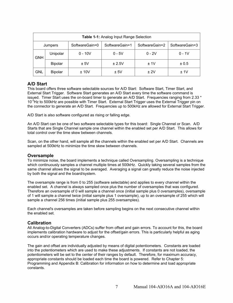
Table 1-1: Analog Input Range Selection
Jumpers SoftwareGain=0 SoftwareGain=1 SoftwareGain=2 SoftwareGain=3
Unipolar 0 - 10V 0 - 5V 0 - 2V 0 - 1V GNH
Bipolar ± 5V ± 2.5V ± 1V ± 0.5
GNL Bipolar ± 10V ± 5V ± 2V ± 1V A/D Start This board offers three software selectable sources for A/D Start: Software Start, Timer Start, and External Start Trigger. Software Start generates an A/D Start every time the software command is issued. Timer Start uses the on-board timer to generate an A/D Start. Frequencies ranging from 2.33 * 10-3Hz to 500kHz are possible with Timer Start. External Start Trigger uses the External Trigger pin on the connector to generate an A/D Start. Frequencies up to 500kHz are allowed for External Start Trigger. A/D Start is also software configured as rising or falling edge. An A/D Start can be one of two software selectable types for this board: Single Channel or Scan. A/D Starts that are Single Channel sample one channel within the enabled set per A/D Start. This allows for total control over the time skew between channels. Scan, on the other hand, will sample all the channels within the enabled set per A/D Start. Channels are sampled at 500kHz to minimize the time skew between channels. Oversample To minimize noise, the board implements a technique called Oversampling. Oversampling is a technique which continuously samples a channel multiple times at 500kHz. Quickly taking several samples from the same channel allows the signal to be averaged. Averaging a signal can greatly reduce the noise injected by both the signal and the board/system. The oversample range is from 0 to 255 (software selectable) and applies to every channel within the enabled set. A channel is always sampled once plus the number of oversamples that was configured. Therefore an oversample of 0 will sample a channel once (initial sample plus 0 oversamples), oversample of 1 will sample a channel twice (initial sample plus 1 oversample), up to an oversample of 255 which will sample a channel 256 times (initial sample plus 255 oversamples). Each channel's oversamples are taken before sampling begins on the next consecutive channel within the enabled set. Calibration All Analog-to-Digital Converters (ADCs) suffer from offset and gain errors. To account for this, the board implements calibration hardware to adjust for the offset/gain errors. This is particularly helpful as aging occurs and/or operating temperature changes. The gain and offset are individually adjusted by means of digital potentiometers. Constants are loaded into the potentiometers which are used to make these adjustments. If constants are not loaded, the potentiometers will be set to the center of their ranges by default. Therefore, for maximum accuracy, appropriate constants should be loaded each time the board is powered. Refer to Chapter 5: Programming and Appendix B: Calibration for information on how to determine and load appropriate constants.
Manual 104-AIO16A and 104-AIO16E 8
A/D FIFO The A/D FIFO buffers the data out of the ADC. This allows conversions to happen without constant CPU intervention. Furthermore, the FIFO's half-full and full flags are readable by software. They can also be used to generate interrupts. If the FIFO becomes full, A/D conversions are paused and resume when at least one A/D sample is read out of the FIFO. Interrupt Request (IRQ) This board can be software enabled to generate an IRQ when the A/D FIFO becomes half-full or full. An IRQ can also be generated after the end of a conversion (EOC) or after the end of a scan (EOS). These IRQs help in taking A/D data off the board quickly. The selection of the IRQ to be used is made by selecting one of the IRQ jumpers on the board. The location of these jumpers is shown in the Option Selection Map. Place a jumper on the posts corresponding to the IRQ you wish to select. If you do not intend on using IRQs, do not install a jumper on any IRQ pins. Analog Outputs (DAC) There are two analog outputs on this board. Each analog output is adjusted by output calibration circuitry including a digital potentiometer. The DACs have two output ranges of 0-5V or 0-10V. These are individually chosen through jumper selections on the board. Refer to the option selection map for the jumper selections. Please note that the DACs are labeled DAC A and DAC B on the PC board but typically referred to as DAC 0 and DAC 1 in the manual. These terms are interchangeable as DAC 0 is the same as DAC A, DAC 1 the same as DAC B. The digital calibration potentiometers are serial devices, with data being entered bit by bit. Although the details of writing bit by bit are described in Appendix B, it is expected that data will be loaded using a software subroutine. Make sure that the correct calibration constants are loaded into the digital potentiometers before using the analog outputs. Refer to Appendix B for calibrating the DACs. Lastly, the DACs have a mode of operation called simultaneous update that will update both DACs simultaneously after DAC1 has been written to. Otherwise, each DAC will update upon being written to. Refer to Chapter 5: Programming for configuration details. Digital I/O This board contains an 8255 like Programmable Peripheral Interface (PPI). There are 2 ports, A and B, available for Digital I/O. Both the low byte (port A) and high byte (port B) can be individually software configured as inputs or outputs. In output mode, each port supports readback of the last written values. Each DIO line is capable of sourcing 24mA or sinking 24mA. By default the DIO lines are pulled up with a 10kΩ resistor to 5V. Counter/Timer The highly versatile 8254 contains three counter/timers. Counter/Timer 0 is available for general purpose use. Counter/Timer 1&2 are dedicated for use in timing A/D starts. The output of Counter/Timer 2 is available on the P2 connector. Counter/Timer 0’s clock and output signals are brought out to the connector. Both signals are buffered and capable of sourcing 24mA or sinking 24mA. Counter/Timer 0’s clock is pulled up with a 10KΩ resistor to 5V. Counter/Timer 0’s clock input is software selectable between an internal 10MHz clock and the external Counter/Timer 0 clock on the P2 connector. The maximum allowed frequency for the clock is 10MHz.

Manual 104-AIO16A and 104-AIO16E 9
Model Options
• -DC Onboard DC/DC converter enables operation from a single +5V power supply • -T Extended Temperature Operation (-40° to +85°C) • -FIFOx “x” = FIFO sample capacity
o 2K, 4K (1K is standard size) • -S0x Special number designator, application specific, contact factory
o Examples: latching I/O connectors; configuration jumpers factory set Included with your board The following items are included with your shipment. Please take time now to ensure that no items are damaged or missing.
1. PC/104 Analog and Digital I/O Module 2. Software Master CD (PDF user manual installed with product package) 3. Printed I/O Quick-Start Guide

Manual 104-AIO16A and 104-AIO16E 10
Chapter 2: Installation
You may wish to refer to the printed I/O Quick Start Guide which was included with your product shipment for specific, quick steps to complete the hardware and software installation.
Software CD Installation
The software provided with this board is contained on one CD and must be installed onto your hard disk prior to use. To do this, perform the following steps as appropriate for your operating system. Substitute the appropriate drive letter for your drive where you see D: in the examples below.
WIN98/Me/2000/XP/2003 a. Place the CD into your CD-ROM drive.
b. The CD should automatically run the install program. If the install program does not run, click START | RUN and type , click OK or press
c. Follow the on-screen prompts to install the software for this board.
LINUX a. Please refer to linux.htm on the CD-ROM for information on installing under linux.
Hardware Installation
Install the software package and set all hardware configuration jumpers (refer to Chapter 3, Option Selection) before plugging the hardware into the system. The SETUP Program can also be used to assist in configuring jumpers on the board. Be especially careful with Address Selection. If the addresses of two installed functions overlap, you will experience unpredictable computer behavior. To help avoid this problem, refer to the FINDBASE.EXE program installed from the CD. The setup program does not set the options on the board, these must be set by jumpers. Caution! * ESD A single static discharge can damage your card and cause premature
failure! Please follow all reasonable precautions to prevent a static discharge such as grounding yourself by touching any grounded surface prior to touching the card.

Manual 104-AIO16A and 104-AIO16E 11
To Install the Board 1. Install jumpers for selected options and base address according to your application
requirements, as mentioned above. 2. Remove power from the PC/104 stack. 3. Assemble standoff hardware for stacking and securing the boards. 4. Carefully plug the board onto the PC/104 connector on the CPU or onto the stack,
ensuring proper alignment of the pins before completely seating the connectors together. 5. Install I/O cables onto the board’s I/O connectors and proceed to secure the stack
together or repeat steps 3-5 until all boards are installed using the selected mounting hardware.
6. Check that all connections in your system are correct and secure then power up the system.
7. Run one of the provided sample programs appropriate for your operating system that was installed from the CD to test and validate your installation.
Figure 2-1: PC/104 Key Information

Manual 104-AIO16A and 104-AIO16E 12
Chapter 3: Option Selection Jumpers are available on the board to configure the following: Base address, IRQ and +/-12V source selection DAC output voltage ranges A/D input mode (single ended or differential), range and bipolar / unipolar selections Software can determine the jumper selections by reading the status register at Base Address +12 (see Chapter 5: Programming for more information). Please refer to the Setup Program on the Software Master CD for additional details of selecting the appropriate options for your application. The standard board has a Counter/Timer, two 12-bit DAC Channels, 16 Bits of Digital I/O, and a 16 channel 16-bit A/D Converter with a 1k sample FIFO. There is an optional version of the board that provides an onboard DC/DC converter. If your PC/104 stack has +5V and +/-12V available, a DC/DC converter is not needed.
IRQ9IRQ10
IRQ11IRQ12IRQ14IRQ15IRQ7IRQ6IRQ5IRQ4IRQ3
BIPOLAR UNIPOLAR
GNH GNL
DIFF
S.E.
0-10V
0-5V
DAC B
DAC A
A5
A6
A7
A8
A9
P2Pin 1
P1
Pin
1P3
DC/DC Option 104 Bus EXT-P3±12V SOURCE SELECT
Figure 3-1: Option Selection Map
The board can take ±12V power from the PC/104 bus, an external source, or an optional DC/DC converter. If the DC/DC converter is installed on the board, the two jumpers next to P3 should not be installed, and their posts may be missing. If no DC/DC converter is present, the jumpers should be installed in their right positions to take ±12V power from the PC/104 bus, or the left positions (toward the edge of the board) to take ±12V power from an external source, provided via P3.

Manual 104-AIO16A and 104-AIO16E 13
Setting the Base Address The following table provides a convenient reference for all address jumper configurations. “YES” indicates the jumper is installed.
A9 A8 A7 A6 A5 Address Range
YES YES YES YES 100h - 11Bh
YES YES YES 120h - 13Bh
YES YES YES 140h - 15Bh
YES YES 160h - 17Bh
YES YES YES 180h - 19Bh
YES YES 1A0h - 1BBh
YES YES 1C0h - 1DBh
YES 1E0h - 1FBh
YES YES YES YES 200h - 21Bh
YES YES YES 220h - 23Bh
YES YES YES 240h - 25Bh
YES YES 260h - 27Bh
YES YES YES 280h - 29Bh
YES YES 2A0h - 2BBh
YES YES 2C0h - 2DBh
YES 2E0h - 2FBh
YES YES YES 300h - 31Bh
YES YES 320h - 33Bh
YES YES 340h - 35Bh
YES 360h - 37Bh
YES YES 380h - 39Bh
YES 3A0h - 3BBh
YES 3C0h - 3DBh
3E0h - 3FBh
Table 3-1: Base Address Jumper Configuration
Manual 104-AIO16A and 104-AIO16E 14
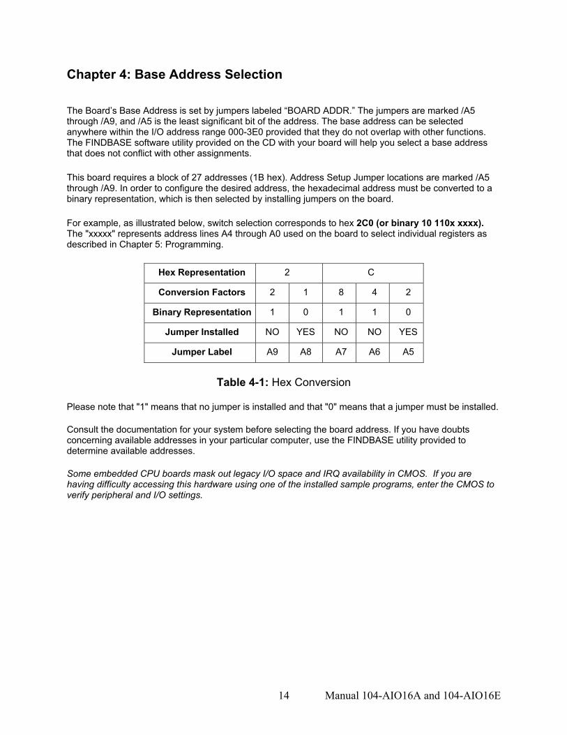
Chapter 4: Base Address Selection
The Board’s Base Address is set by jumpers labeled “BOARD ADDR.” The jumpers are marked /A5 through /A9, and /A5 is the least significant bit of the address. The base address can be selected anywhere within the I/O address range 000-3E0 provided that they do not overlap with other functions. The FINDBASE software utility provided on the CD with your board will help you select a base address that does not conflict with other assignments. This board requires a block of 27 addresses (1B hex). Address Setup Jumper locations are marked /A5 through /A9. In order to configure the desired address, the hexadecimal address must be converted to a binary representation, which is then selected by installing jumpers on the board. For example, as illustrated below, switch selection corresponds to hex 2C0 (or binary 10 110x xxxx). The "xxxxx" represents address lines A4 through A0 used on the board to select individual registers as described in Chapter 5: Programming.
Hex Representation 2 C
Conversion Factors 2 1 8 4 2
Binary Representation 1 0 1 1 0
Jumper Installed NO YES NO NO YES
Jumper Label A9 A8 A7 A6 A5
Table 4-1: Hex Conversion
Please note that "1" means that no jumper is installed and that "0" means that a jumper must be installed. Consult the documentation for your system before selecting the board address. If you have doubts concerning available addresses in your particular computer, use the FINDBASE utility provided to determine available addresses. Some embedded CPU boards mask out legacy I/O space and IRQ availability in CMOS. If you are having difficulty accessing this hardware using one of the installed sample programs, enter the CMOS to verify peripheral and I/O settings.

Manual 104-AIO16A and 104-AIO16E 15
Chapter 5: Programming A/D Order of Operations: Behavior may become unpredictable if these steps are not followed. This is a guide of steps to take before beginning an A/D conversion. 1) Configure the channel gains (Base Address + 2-5). 2) Configure the start and end channel (Base Address + 6). 3) Configure the number of oversamples per channel (Base Address + 7). 4) Configure Counter/Timer 1&2 if using Timer Start or External Start Trigger (Base Address + 8- B). If using External Start Trigger, connect the trigger source to P2 pin 39. 5) Configure the A/D Start Source as Software Start, Timer Start, or External Start Trigger. Configure A/D Start as rising or falling edge. Configure A/D Start as Single Channel or Scan. (Base Address + 11). Once this address is written to, A/D conversions will be enabled if the A/D Start Source is either Timer Start or External Start Trigger. If the A/D Start Source is Software Start, conversions will begin after a write to Base Address + 1. 6) Read A/D data from the A/D Data FIFO with a read from Base Address + 0-1. It is helpful to use the flags in Base Address + 12 and the IRQ flags in Base Address + 13 when deciding to read A/D data.
Offset Write Function Read Function 0 1 A/D Software Start
A/D Data
2 3 4 5
A/D Programmable Gain Configuration
6 A/D Start/End Ch Configuration 7 A/D Oversample Configuration 8 9 A B
Counter/Timer Configuration Counter/Timer Configuration
C D
DAC 0 Output Data
E F
DAC 1 Output Data
10 DAC Configuration
11 A/D Start & Counter/Timer 0 Clock Configuration
12 A/D, DAC, FIFO Status Flags 13 IRQ Configuration IRQ Status 14 Port A DIO (8255) Port A DIO (8255) 15 Port B DIO (8255) Port B DIO (8255) 16 17 DIO Configuration (8255) 18 EEPROM access EEPROM access 19 Calibration access 1A 1B Reset Register
1C-1E 1F Board Model
Table 5-1: Register Definitions

Manual 104-AIO16A and 104-AIO16E 16
NOTE: Reading and writing words (16 bits) may only be done on even address boundaries (ie: Base Address + 0, + 2, etc). Reading and writing bytes (8 bits) can be done on even or odd boundaries. Base Address + 0-1 (read) A/D Data Base Address +0
Bit 7 Bit 6 Bit 5 Bit 4 Bit 3 Bit 2 Bit 1 Bit 0 ad7 ad6 ad5 ad4 ad3 ad2 ad1 ad0
Base Address +1 Bit 7 Bit 6 Bit 5 Bit 4 Bit 3 Bit 2 Bit 1 Bit 0 ad15 ad14 ad13 ad12 ad11 ad10 ad9 ad8
ad15-ad0 -> A/D data
Reading a word from Base Address + 0 or two consecutive byte reads, first Base Address + 0 and then Base Address + 1, will grab one conversion’s data from the A/D FIFO. If issuing two byte reads, it is important to know that the A/D FIFO increments to the next conversion’s data only after the byte read from Base Address + 1. The byte read from Base Address + 0 must be done before the byte read from Base Address + 1 or the lower data byte will be lost.
Base Address + 1 (write) A/D Software Start
Bit 7 Bit 6 Bit 5 Bit 4 Bit 3 Bit 2 Bit 1 Bit 0 Software start
Writing any value to this address will begin one A/D Start.
Base Address + 2-5 (write) A/D Programmable Gain Configuration Base Address +2
Bit 7 Bit 6 Bit 5 Bit 4 Bit 3 Bit 2 Bit 1 Bit 0 Ch3 SoftwareGain Ch2 SoftwareGain Ch1 SoftwareGain Ch0 SoftwareGain
Base Address +3 Bit 7 Bit 6 Bit 5 Bit 4 Bit 3 Bit 2 Bit 1 Bit 0 Ch7 SoftwareGain Ch6 SoftwareGain Ch5 SoftwareGain Ch4 SoftwareGain
Base Address +4 Bit 7 Bit 6 Bit 5 Bit 4 Bit 3 Bit 2 Bit 1 Bit 0
Ch11 SoftwareGain Ch10 SoftwareGain Ch9 SoftwareGain Ch8 SoftwareGain
Base Address +5 Bit 7 Bit 6 Bit 5 Bit 4 Bit 3 Bit 2 Bit 1 Bit 0
Ch15 SoftwareGain Ch14 SoftwareGain Ch13 SoftwareGain Ch12 SoftwareGain softwareGain = "00" = 0 softwareGain = "01" = 1 softwareGain = "10" = 2 softwareGain = "11" = 3

Manual 104-AIO16A and 104-AIO16E 17
Writing to these addresses will set the Software Gain per channel (see Table 1-1: Analog Input Range Selection)
Base Address + 6 (write) A/D Start/End Channel Configuration Bit 7 Bit 6 Bit 5 Bit 4 Bit 3 Bit 2 Bit 1 Bit 0 end3 end2 end1 end0 start3 start2 start1 start0
start3-start0 -> A/D start channel (0-15) end3-end0 -> A/D end channel (0-15)
Writing to this address will set the start and end address of the enabled set of channels.
Base Address + 7 (write) A/D Oversample Configuration
Bit 7 Bit 6 Bit 5 Bit 4 Bit 3 Bit 2 Bit 1 Bit 0 overSamp7 overSamp6 overSamp5 overSamp4 overSamp3 overSamp2 overSamp1 overSamp0
overSamp7-overSamp0 -> Channel Oversample (0-255) Writing to this address will set the number of oversamples to take per channel.
Base Address + 8-B Counter/Timer Configuration Counter/Timer 0 is fully programmable for general use. Counter/Timer 1&2 are concatenated together (output of Counter/Timer 1 is routed to the clock input of Counter/Timer 2). The concatenated Counter/Timer 1&2 are used for A/D Start: both Timer Start and External Start Trigger. The output of Counter/Timer 2 is the source for the aforementioned A/D Starts. The output of Counter/Timer 2 is available on Pin 43 of connector P2.
For detailed information on programming the 8254 Counter/Timer device, please refer to Appendix A.
Base Address + C-D (write) DAC 0 Output Data Base Address + C
Bit 7 Bit 6 Bit 5 Bit 4 Bit 3 Bit 2 Bit 1 Bit 0 da7 da6 da5 da4 da3 da2 da1 da0
Base Address + D
Bit 7 Bit 6 Bit 5 Bit 4 Bit 3 Bit 2 Bit 1 Bit 0 X X X X da11 da10 da9 da8
da11-da0 -> DAC 0 data Writing a 12-bit value to this address will output the corresponding voltage on DAC 0 (refer the Option Selection map for output voltage range). If the DAC simultaneous bit (Base Address + 10, bit 1) is set, then DAC 0’s output will update after writing to DAC 1.

Manual 104-AIO16A and 104-AIO16E 18
Base Address + E-F (write) DAC 1 Output Data Base Address + E
Bit 7 Bit 6 Bit 5 Bit 4 Bit 3 Bit 2 Bit 1 Bit 0 da7 da6 da5 da4 Da3 da2 da1 da0
Base Address + F
Bit 7 Bit 6 Bit 5 Bit 4 Bit 3 Bit 2 Bit 1 Bit 0 X X X X da11 da10 da9 da8
da11-da0 -> DAC 1 data Writing a 12-bit value to this address will output the corresponding voltage on DAC 1 (refer the Option Selection map for output voltage range).
Base Address + 10 (write) DAC Configuration Bit 7 Bit 6 Bit 5 Bit 4 Bit 3 Bit 2 Bit 1 Bit 0
X X X X X X X simultaneous
simultaneous -> '0' = DACs update when written '1' = DACs update upon write to DAC 1 Writing a ‘1’ to Bit 0 will set the DAC simultaneous bit. This causes both DACs to be updated on a write to DAC 1. Base Address + 11 (write) A/D Start & Counter/Timer 0 Clock Configuration
Bit 7 Bit 6 Bit 5 Bit 4 Bit 3 Bit 2 Bit 1 Bit 0 X X X clkSrc startEdge startType startSource1 startSource0
Writing to this address will configure the A/D Start Source, A/D Start Type, A/D Start as rising or falling edge, and Counter/Timer 0’s clock source. Below are the different configuration bit patterns:
A/D Start Source • Software startSource0 = ‘0’; startSource1 = ‘0’ • Timer startSource0 = ‘1’; startSource1 = ‘0’ • External startSource0 = ‘0’; startSource1 = ‘1’
A/D Start Type
• Single Channel startType = ‘0’ • Scan startType = ‘1’
A/D Start Edge
• Rising startEdge = ‘0’ • Falling startEdge = ‘1’
Counter/Timer0 Clock
• Internal 10MHz clkSrc = ‘0’ • External Pin clkSrc = ‘1’

Manual 104-AIO16A and 104-AIO16E 19
Base Address + 12 (read) A/D, DAC, FIFO Status Flags Bit 7 Bit 6 Bit 5 Bit 4 Bit 3 Bit 2 Bit 1 Bit 0
fifoFull halfFull empty dac1 dac0 gainMode single-ended bipolar
Reading from this address will show the status of the following flags:
bipolar ‘0’ = jumpers set to unipolar ‘1’ = jumpers set to bipolar single-ended ‘0’ = jumpers set to differential ‘1’ = jumpers set to single-ended gainMode ‘0’ = jumpers set to GNL ‘1’ = jumpers set to GNH dac0 ‘0’ = DAC 0 has 0-10V range ‘1’ = DAC 0 has 0-5V range dac1 ‘0’ = DAC 1 has 0-10V range ‘1’ = DAC 1 has 0-5V range empty ‘0’ = A/D Data FIFO is empty ‘1’ = A/D Data FIFO is not empty halfFull ‘0’ = A/D FIFO is at least half full ‘1’ = A/D FIFO is not at least half full fifoFull ‘0’ = A/D Data FIFO is full ‘1’ = A/D Data FIFO is not full Base Address + 13 (read/write) IRQ Configuration and Status Base Address + 13 write
Bit 7 Bit 6 Bit 5 Bit 4 Bit 3 Bit 2 Bit 1 Bit 0 X X X X fullIrqEn halfFullIrqEn eosIrqEn eocIrqEn
Writing to this address will configure the IRQs for End of Conversion (EOC), End of Scan (EOS), A/D Data FIFO at least half full, and A/D Data FIFO full. Below are the IRQ enable bit patterns: eocIrqEn ‘0’ = disable the EOC IRQ ‘1’ = enable the EOC IRQ eosIrqEn ‘0’ = disable the EOS IRQ ‘1’ = enable the EOS IRQ halfFullIrqEn ‘0’ = disable the A/D Data FIFO ‘1’ = enable the A/D Data FIFO is at least half full IRQ is at least half full IRQ fullIrqEn ‘0’ = disable the A/D Data FIFO ‘1’ = enable the A/D Data FIFO full IRQ full IRQ Base Address + 13 read
Bit 7 Bit 6 Bit 5 Bit 4 Bit 3 Bit 2 Bit 1 Bit 0 fullIrq halfFullIrq eosIrq eocIrq X X X X
Once any of the above IRQ enables are set to ‘1’, the corresponding condition will cause an IRQ to be generated. All four enables can be set at the same time. A read of this address allows the ability to see which IRQ flag generated the IRQ. Below are the IRQ flags: eocIrq ‘0’ = no EOC IRQ occurred ‘1’ = EOC IRQ occurred eosIrq ‘0’ = no EOS IRQ occurred ‘1’ = EOS IRQ occurred halfFullIrq ‘0’ = no A/D FIFO is at least ‘1’ = A/D FIFO is at least half full IRQ occurred half full IRQ occurred fullIrq ‘0’ = no FIFO full IRQ occurred ‘1’ = FIFO full IRQ occurred Reading this address also clears any of the IRQ flags that are set.

Manual 104-AIO16A and 104-AIO16E 20
Base Address + 14 (read/write) Port A DIO (8255) Bit 7 Bit 6 Bit 5 Bit 4 Bit 3 Bit 2 Bit 1 Bit 0 a7 a6 a5 a4 a3 a2 a1 a0
a7-a0 -> Port A data Reading from this address will return the digital data on Port A. Writing to this address will output the digital data on Port A. Readback is supported while in the output mode. Be sure to refer to Base Address + 17 for controlling Port A’s input/output direction. Base Address + 15 (read/write) Port B DIO (8255)
Bit 7 Bit 6 Bit 5 Bit 4 Bit 3 Bit 2 Bit 1 Bit 0 b7 b6 b5 b4 b3 b2 b1 b0
b7-b0 -> Port B data Reading from this address will return the digital data on Port B. Writing to this address will output the digital data on Port B. Readback is supported while in the output mode. Be sure to refer to Base Address + 17 for controlling Port B’s input/output direction. Base Address + 16 Unused Base Address + 17 (write) DIO Configuration (8255)
Bit 7 Bit 6 Bit 5 Bit 4 Bit 3 Bit 2 Bit 1 Bit 0 modeSetFlag X X PortADir X X portBDir X
Writing to this address configures the input/output direction for Ports A and B. A ‘1’ must always be written to bit 7 when configuring. Below are the Port direction bits: modeSetFlag ‘0’ = configuration not enabled ‘1’ = configuration enabled portADir ‘0’ = Port A is output ‘1’ = Port A is input (default) portBDir ‘0’ = Port B is output ‘1’ = Port B is input (default) Base Address + 18 (read/write) EEPROM access Base Address + 18 read
Bit 7 Bit 6 Bit 5 Bit 4 Bit 3 Bit 2 Bit 1 Bit 0 data X X X X X X X
Base Address + 18 write
Bit 7 Bit 6 Bit 5 Bit 4 Bit 3 Bit 2 Bit 1 Bit 0 data X X X X X X SClk
The EEPROM is intended to hold calibration data for the A/D Gain and Offset correction, and the Gain Correction data for both DACs. Calibration is only needed for GNL/GNH and BIP/UNI jumper selected ranges, so a total of 4 A/D Input calibration data pairs are used. Consult the provided calibration program or sample code for information on the locations in the EEPROM used to store the calibration data. Although the EEPROM is intended to contain calibration data, it is unlikely your program will need to keep calibration data for the ranges you are not going to use. In this case you can use those locations in the EEPROM for your own purposes.
Manual 104-AIO16A and 104-AIO16E 21
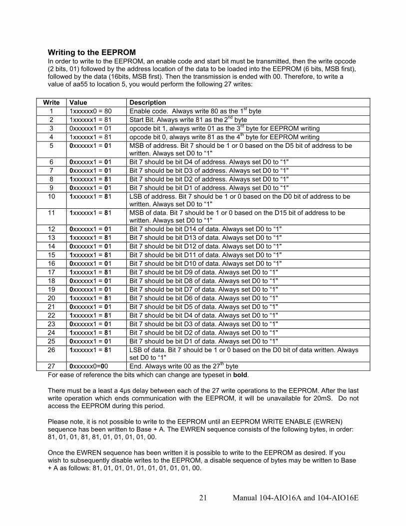
Writing to the EEPROM In order to write to the EEPROM, an enable code and start bit must be transmitted, then the write opcode (2 bits, 01) followed by the address location of the data to be loaded into the EEPROM (6 bits, MSB first), followed by the data (16bits, MSB first). Then the transmission is ended with 00. Therefore, to write a value of aa55 to location 5, you would perform the following 27 writes:
Write Value Description 1 1xxxxxx0 = 80 Enable code. Always write 80 as the 1st byte 2 1xxxxxx1 = 81 Start Bit. Always write 81 as the 2nd byte 3 0xxxxxx1 = 01 opcode bit 1, always write 01 as the 3rd byte for EEPROM writing 4 1xxxxxx1 = 81 opcode bit 0, always write 81 as the 4th byte for EEPROM writing 5 0xxxxxx1 = 01 MSB of address. Bit 7 should be 1 or 0 based on the D5 bit of address to be
written. Always set D0 to “1" 6 0xxxxxx1 = 01 Bit 7 should be bit D4 of address. Always set D0 to “1" 7 0xxxxxx1 = 01 Bit 7 should be bit D3 of address. Always set D0 to “1" 8 1xxxxxx1 = 81 Bit 7 should be bit D2 of address. Always set D0 to “1" 9 0xxxxxx1 = 01 Bit 7 should be bit D1 of address. Always set D0 to “1"
10 1xxxxxx1 = 81 LSB of address. Bit 7 should be 1 or 0 based on the D0 bit of address to be written. Always set D0 to “1"
11 1xxxxxx1 = 81 MSB of data. Bit 7 should be 1 or 0 based on the D15 bit of address to be written. Always set D0 to “1"
12 0xxxxxx1 = 01 Bit 7 should be bit D14 of data. Always set D0 to “1" 13 1xxxxxx1 = 81 Bit 7 should be bit D13 of data. Always set D0 to “1" 14 0xxxxxx1 = 01 Bit 7 should be bit D12 of data. Always set D0 to “1" 15 1xxxxxx1 = 81 Bit 7 should be bit D11 of data. Always set D0 to “1" 16 0xxxxxx1 = 01 Bit 7 should be bit D10 of data. Always set D0 to “1" 17 1xxxxxx1 = 81 Bit 7 should be bit D9 of data. Always set D0 to “1" 18 0xxxxxx1 = 01 Bit 7 should be bit D8 of data. Always set D0 to “1" 19 0xxxxxx1 = 01 Bit 7 should be bit D7 of data. Always set D0 to “1" 20 1xxxxxx1 = 81 Bit 7 should be bit D6 of data. Always set D0 to “1" 21 0xxxxxx1 = 01 Bit 7 should be bit D5 of data. Always set D0 to “1" 22 1xxxxxx1 = 81 Bit 7 should be bit D4 of data. Always set D0 to “1" 23 0xxxxxx1 = 01 Bit 7 should be bit D3 of data. Always set D0 to “1" 24 1xxxxxx1 = 81 Bit 7 should be bit D2 of data. Always set D0 to “1" 25 0xxxxxx1 = 01 Bit 7 should be bit D1 of data. Always set D0 to “1" 26 1xxxxxx1 = 81 LSB of data. Bit 7 should be 1 or 0 based on the D0 bit of data written. Always
set D0 to “1" 27 0xxxxxx0=00 End. Always write 00 as the 27th byte For ease of reference the bits which can change are typeset in bold. There must be a least a 4µs delay between each of the 27 write operations to the EEPROM. After the last write operation which ends communication with the EEPROM, it will be unavailable for 20mS. Do not access the EEPROM during this period. Please note, it is not possible to write to the EEPROM until an EEPROM WRITE ENABLE (EWREN) sequence has been written to Base + A. The EWREN sequence consists of the following bytes, in order: 81, 01, 01, 81, 81, 01, 01, 01, 01, 00. Once the EWREN sequence has been written it is possible to write to the EEPROM as desired. If you wish to subsequently disable writes to the EEPROM, a disable sequence of bytes may be written to Base + A as follows: 81, 01, 01, 01, 01, 01, 01, 01, 01, 00.

Manual 104-AIO16A and 104-AIO16E 22
Reading from the EEPROM Similarly, reading a word takes 10 writes (enable code, start bit, read opcode (2 bits 1,0) and the address (6 bits, MSB first)), followed by 16 reads to acquire the data from the EEPROM, followed by one write to terminate communication with the EEPROM. Therefore, to read from address 4, perform the following writes and reads:
Write Value Description 1 1xxxxxx0 = 80 Enable code. Always write 80 as the 1st byte 2 1xxxxxx1 = 81 Start Bit. Always write 81 as the 2nd byte. 3 1xxxxxx1 = 81 Opcode Bit 1. Always write 81 as the 3rd byte for reading 4 0xxxxxx1 = 01 Opcode Bit 0. Always write 01 as the 4th byte for reading 5 0xxxxxx1 = 01 MSB of address. Bit 7 should be 1 or 0 based on the D5 bit of address in the
EEPROM to be Read. Always set D0 to “1" 6 0xxxxxx1 = 01 Bit 7 should be bit D4 of address. Always set D0 to “1" 7 0xxxxxx1 = 01 Bit 7 should be bit D3 of address. Always set D0 to “1" 8 1xxxxxx1 = 81 Bit 7 should be bit D2 of address. Always set D0 to “1" 9 0xxxxxx1 = 01 Bit 7 should be bit D1 of address. Always set D0 to “1"
10 0xxxxxx1 = 01 LSB of address. Bit 7 should be 1 or 0 based on the D0 bit of address to be read. Always set D0 to “1"
Read 1 Bit D7 of this Read returns the Most Significant Bit (D15) of the 16-bit data stored at the address specified in writes 4 through 9.
Read 2 D7 contains bit D14 from the word at the specified address Read 3 D7 contains bit D13 from the word at the specified address Read 4 D7 contains bit D12 from the word at the specified address Read 5 D7 contains bit D11 from the word at the specified address Read 6 D7 contains bit D10 from the word at the specified address Read 7 D7 contains bit D9 from the word at the specified address Read 8 D7 contains bit D8 from the word at the specified address Read 9 D7 contains bit D7 from the word at the specified address Read 10 D7 contains bit D6 from the word at the specified address Read 11 D7 contains bit D5 from the word at the specified address Read 12 D7 contains bit D4 from the word at the specified address Read 13 D7 contains bit D3 from the word at the specified address Read 14 D7 contains bit D2 from the word at the specified address Read 15 D7 contains bit D1 from the word at the specified address Read 16 D7 contains bit D0 from the word at the specified address Write 11 0xxxxxx0 = 00 End. Always write 00 as the last step
For ease of reference the bits which can change are typeset in bold. There must be a least a 4µs delay between each of the 11 write and 16 read operations to the EEPROM. After the last write operation which ends communication with the EEPROM, it will be unavailable for 20mS. Do not access the EEPROM during this period. The Software Master CD contains sample programs demonstrating the use of the EEPROM in a variety of languages, including a “driverlet” which encapsulates the complexities of the process. Using this “driverlet” is as simple as passing the address and data in the EEPROM you wish to write, or the address from which to read, to our functions. It is highly recommended that you use the provided source code as a basis for your own programs.

Manual 104-AIO16A and 104-AIO16E 23
Base Address + 19 (write) Calibration access Bit 7 Bit 6 Bit 5 Bit 4 Bit 3 Bit 2 Bit 1 Bit 0 data X X X X X X SClk
The board contains 4 digital potentiometers used to calibrate the device. The four calibration corrections provided are: A/D Offset (00), A/D Gain (01), Gain for DAC0 (10), and DAC1 (11). These four corrections are internally addressed 0, 1, 2, and 3. Each calibration correction consists of a value from 0 - 255 (8 bits) corresponding to the internal value of the digital potentiometer. A/D Offset corresponds to the “B” in a Y=mX+B equation. A/D Gain is the “m” term of the same equation. DAC Gain represents “m” in the equation Y=mX. The nature of the DAC circuitry eliminates the need to provide offset (B) calibration. The value you load into these calibration potentiometers is normally read from the EEPROM and written here only during program initialization, and only needs to be written once per power-on cycle. To load one of the calibration correction values you must write the address (0-3) of the correction you wish to load, the 8-bit value you wish to load, and an End byte. Similar to the operation of the EEPROM, the calibration correction values are loaded serially into the digital potentiometers in the board. Therefore, to load a value of 4F into the A/D Gain potentiometer, the following writes are performed: Write Value Description 1 1xxxxxx0=80 Enable code. Always write 80 as the 1st byte 2 0xxxxxx1=01 3 1xxxxxx1=81
These two bits are the address of the potentiometer to write. 00 is A/D offset, 01 is gain, 10 is DAC0 gain, 11 is DAC1 gain. Write 2 is MSB, Write 3 is LSB.
4 0xxxxxx1=01 MSB of data. Bit D7 of Write 4 should be the D7 bit of the calibration correction value you are loading.
5 1xxxxxx1=81 D7 should be bit D6 of the calibration value 6 0xxxxxx1=01 D7 should be bit D5 of the calibration value 7 0xxxxxx1=01 D7 should be bit D4 of the calibration value 8 1xxxxxx1=81 D7 should be bit D3 of the calibration value 9 1xxxxxx1=81 D7 should be bit D2 of the calibration value 10 1xxxxxx1=81 D7 should be bit D1 of the calibration value 11 1xxxxxx1=81 D7 should be bit D0 of the calibration value 12 0xxxxxx1=01 End. Always Write 00 as the last step
For ease of reference the bits which can change are typeset in bold. For details on the operation of the Digital Potentiometer, refer to the Analog Devices AD8403 datasheet. Base Address + 1A Unused Base Address + 1B (write) Reset Register
Bit 7 Bit 6 Bit 5 Bit 4 Bit 3 Bit 2 Bit 1 Bit 0 X X X masterReset dacReset dioReset digPotReset fifoReset
Writing to this address will reset the following: fifoReset ‘0’ = N/A ‘1’ = reset the A/D Data FIFO digPotReset ‘0’ = N/A ‘1’ = reset the digital calibration potentiometers dioReset ‘0’ = N/A ‘1’ = reset the 8255 Port A and Port B dacReset ‘0’ = N/A ‘1’ = reset the DACs back to zero masterReset ‘0’ = N/A ‘1’ = reset all of the above + all configuration addresses

Manual 104-AIO16A and 104-AIO16E 24
Base Address + 1C – 1E Unused Base Address + 1F (read) Board Model
Bit 7 Bit 6 Bit 5 Bit 4 Bit 3 Bit 2 Bit 1 Bit 0 0 0 0 0 0 0 104E 104A
Reading from this address will indicate the presence and model number, or absence of the board. 104A ‘0’ = N/A ‘1’ = “104A” model detected Byte value = “01” 104E ‘0’ = N/A ‘1’ = “104E” model detected Byte value = “02” No card detected Byte value = “FF”

Manual 104-AIO16A and 104-AIO16E 25
Chapter 6: Connector Pin Assignments
Pin Signal Name Description Pin Signal Name Description
1 Ch0(SE)/Ch0+(DIFF) Channel 0 Singled-ended or Channel 0 differential non-inverting input 2 Ch8(SE)/Ch0-(DIFF) Channel 8 Single-ended or
Channel 0 differential inverting input
3 AGND Analog Ground 4 Ch9(SE)/Ch1-(DIFF) Channel 9 Single-ended or Channel 1 differential inverting input
5 Ch1(SE)/Ch1+(DIFF) Channel 1 Singled-ended or Channel 1 differential non-inverting input 6 AGND Analog Ground
7 Ch2(SE)/Ch2+(DIFF) Channel 2 Singled-ended or Channel 2 differential non-inverting input 8 Ch10(SE)/Ch2-(DIFF) Channel 10 Single-ended or
Channel 2 differential inverting input
9 AGND Analog Ground 10 Ch11(SE)/Ch3-(DIFF) Channel 11 Single-ended or Channel 3 differential inverting input
11 Ch3(SE)/Ch3+(DIFF) Channel 3 Singled-ended or Channel 3 differential non-inverting input 12 AGND Analog Ground
13 Ch4(SE)/Ch4+(DIFF) Channel 4 Singled-ended or Channel 4 differential non-inverting input 14 Ch12(SE)/Ch4-(DIFF) Channel 12 Single-ended or
Channel 4 differential inverting input
15 AGND Analog Ground 16 Ch13(SE)/Ch5-(DIFF) Channel 13 Single-ended or Channel 5 differential inverting input
17 Ch5(SE)/Ch5+(DIFF) Channel 5 Singled-ended or Channel 5 differential non-inverting input 18 AGND Analog Ground
19 Ch6(SE)/Ch6+(DIFF) Channel 6 Singled-ended or Channel 6 differential non-inverting input 20 Ch14(SE)/Ch6-(DIFF) Channel 14 Single-ended or
Channel 6 differential inverting input
21 AGND Analog Ground 22 Ch15(SE)/Ch7-(DIFF) Channel 15 Single-ended or Channel 7 differential inverting input
23 Ch7(SE)/Ch7+(DIFF) Channel 7 Singled-ended or Channel 7 differential non-inverting input 24 AGND Analog Ground
25 DAC 0 Digital to Analog Output Channel 0 26 DAC 1 Digital to Analog Output Channel 1
Table 6-1: P1, 26-pin Right-Angle Header, Analog Inputs, Analog Outputs
Manual 104-AIO16A and 104-AIO16E 26
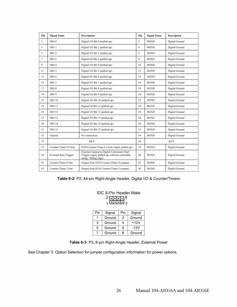
Pin Signal Name Description Pin Signal Name Description
1 DIO 0 Digital I/O Bit 0 (pulled-up) 2 DGND Digital Ground
3 DIO 1 Digital I/O Bit 1 (pulled-up) 4 DGND Digital Ground
5 DIO 2 Digital I/O Bit 2 (pulled-up) 6 DGND Digital Ground
7 DIO 3 Digital I/O Bit 3 (pulled-up) 8 DGND Digital Ground
9 DIO 4 Digital I/O Bit 4 (pulled-up) 10 DGND Digital Ground
11 DIO 5 Digital I/O Bit 5 (pulled-up) 12 DGND Digital Ground
13 DIO 6 Digital I/O Bit 6 (pulled-up) 14 DGND Digital Ground
15 DIO 7 Digital I/O Bit 7 (pulled-up) 16 DGND Digital Ground
17 DIO 8 Digital I/O Bit 8 (pulled-up) 18 DGND Digital Ground
19 DIO 9 Digital I/O Bit 9 (pulled-up) 20 DGND Digital Ground
21 DIO 10 Digital I/O Bit 10 (pulled-up) 22 DGND Digital Ground
23 DIO 11 Digital I/O Bit 11 (pulled-up) 24 DGND Digital Ground
25 DIO 12 Digital I/O Bit 12 (pulled-up) 26 DGND Digital Ground
27 DIO 13 Digital I/O Bit 13 (pulled-up) 28 DGND Digital Ground
29 DIO 14 Digital I/O Bit 14 (pulled-up) 30 DGND Digital Ground
31 DIO 15 Digital I/O Bit 15 (pulled-up) 32 DGND Digital Ground
33 Unused No connection 34 DGND Digital Ground
35 KEY 36 KEY
37 Counter/Timer 0 Clock 8254 Counter/Timer 0 Clock (input; pulled up) 38 DGND Digital Ground
39 External Start Trigger External Analog to Digital Conversion Start Trigger (input; pulled-up; software selectable rising / falling edge)
40 DGND Digital Ground
41 Counter/Timer 0 Out Output from 8254 Counter/Timer 0 (output) 42 DGND Digital Ground
43 Counter/Timer 2 Out Output from 8254 Counter/Timer 2 (output) 44 DGND Digital Ground
Table 6-2: P2, 44-pin Right-Angle Header, Digital I/O & Counter/Timers
Pin Signal Pin Signal 1 Ground 2 Ground 3 Ground 4 +12V 5 Ground 6 -12V 7 Ground 8 Ground
Table 6-3: P3, 8-pin Right-Angle Header, External Power
See Chapter 3: Option Selection for jumper configuration information for power options.

Manual 104-AIO16A and 104-AIO16E 27
Chapter 7: Specifications
Analog Inputs ADC Type Successive approximation Sampling rate “16A” version: 500ksamples/sec (maximum aggregate) “16E” version: 250ksamples/sec (maximum aggregate) Resolution 16-bit Number of channels 16 single-ended or 8 differential (jumper selectable) Bipolar ranges ±0.5V, ±1, ±2V, ±2.5V, ±5V, and ±10V (jumper+software selectable) Unipolar ranges 0-1V, 0-2V, 0-5V, 0-10V (jumper+software selectable) Board Calibration Programmable Digital Potentiometers to calibrate for gain/offset error System Calibration Program provided to calibrate entire system Input impedance 1MΩ A/D Start Sources Software Start, Timer Start, and External Start Trigger (rising or falling edge; software selectable) A/D Start Types Single Channel or Scan (software selectable) Channel Oversampling 0-255 consecutive samples/channel (software selectable) Overvoltage protection -40 to +55V Crosstalk 60dB @ 400kHz Analog Outputs Channels 2 Resolution 12-bit Voltage Ranges 0-5V, 0-10V (jumper selectable) Conversion Frequency 100k conversions/sec Simultaneous Update Yes Digital I/O Type 8255 (Port A and Port B only) Lines 16, programmable as inputs or outputs in groups of 8 (pulled-up) Input voltage Logic low: 0V(min) to 0.8V(max)
Logic high: 2V(min) to 5V(max) Output voltage Logic low: 0V(min) to 0.55V(max) Logic high: 2V(min) to 5V(max) Output current Logic low 24mA(max) sink Logic high 24mA(max) source Counter/Timer Type 82C54 programmable interval counter Available Counters Counter 0 Input Frequency 10MHz (max) Counter size 16-bit Clock Internal 10MHz or Externally supplied (software selectable; pulled-up) Clock Period 100ns (min) Clock Pulse Width High/Low 30ns (min)/40ns (min) Input/Output Voltage/Current Same as Digital I/O Environmental Operating Temperature 0° to +70°C, optional -40° to +85°C Storage Temperature -40° to +105°C Humidity 5% to 90% RH, without condensation Power required Bus powered: +5V at 40mA typical w/ no external I/O connections
+12V at 24mA “” -12V at 23mA “” DC/DC option: +5V at 180mA typical w/ no ext. I/O connections

Manual 104-AIO16A and 104-AIO16E 28
Appendix A: 82C54 Counter Timer Operation The board contains one type 8254 programmable counter/timer. The 8254 consists of three, 16-bit, presettable down-counters. Each counter can be programmed to any count between 2 and 65,535 in binary format, depending on the mode chosen. The programmed value is a divisor and the output frequency equals the input frequency divided by the programmed value. In this manual these three counter/timers are designated Counter/Timer 0, Counter/Timer 1, and Counter/Timer 2. Counter/Timer 0 is for general use. Counter/Timer 1’s output in the clock input to Counter/Timer 2. The output of Counter/Timer 2 is used for A/D Start or for general use (timer not needed for A/D Start). Refer to the block diagram for more information. Operational Modes The 8254 modes of operation are described in the following paragraphs to familiarize you with the versatility and power of this device. For those interested in more detailed information, a full description of the 8254 programmable interval timer can be found in the Intel (or equivalent manufacturers) data sheets. The following conventions apply for use in describing operation of the 8254 : Clock: A positive pulse into the counter's clock input. Trigger: A rising edge input to the counter's gate input. Counter Loading: Programming of a binary count into the counter.
Mode 0: Pulse on Terminal Count After the counter is loaded, the output is set low and will remain low until the counter decrements to zero. The output then goes high and remains high until a new count is loaded into the counter. A trigger enables the counter to start decrementing.
Mode 1: Retriggerable One-Shot The output goes low on the clock pulse following a trigger to begin the one-shot pulse and goes high when the counter reaches zero. Additional triggers result in reloading the count and starting the cycle over. If a trigger occurs before the counter decrements to zero, a new count is loaded. Thus, this forms a re-triggerable one-shot. In mode 1, a low output pulse is provided with a period equal to the counter count-down time.
Mode 2: Rate Generator This mode provides a divide-by-N capability where N is the count loaded into the counter. When triggered, the counter output goes low for one clock period after N counts, reloads the initial count, and the cycle starts over. This mode is periodic, the same sequence is repeated indefinitely until the gate input is brought low.
Mode 3: Square Wave Generator This mode operates periodically like mode 2. The output is high for half of the count and low for the other half. If the count is even, then the output is a symmetrical square wave. If the count is odd, then the output is high for (N+1)/2 counts and low for (N-1)/2 counts. Periodic triggering or frequency synthesis are two possible applications for this mode. Note that in this mode, to achieve the square wave, the counter decrements by two for the total loaded count, then reloads and decrements by two for the second part of the wave form.

Manual 104-AIO16A and 104-AIO16E 29
Mode 4: Software Triggered Strobe This mode sets the output high and, when the count is loaded, the counter begins to count down. When the counter reaches zero, the output will go low for one input period. The counter must be reloaded to repeat the cycle. A low gate input will inhibit the counter. This mode can be used to provide a delayed software trigger for initiating A/D conversions.
Mode 5: Hardware Triggered Strobe In this mode, the counter will start counting after the rising edge of the trigger input and will go low for one clock period when the terminal count is reached. The counter is retriggerable. The output will not go low until the full count after the rising edge of the trigger. Programming On this card the 8254 counters occupy the following addresses (hex): Base Address + 8: Read/Write Counter 0 Base Address + 9: Read/Write Counter 1 Base Address + A: Read/Write Counter 2 Base Address + B: Write to Counter Control register The counters are programmed by writing a control byte into a counter control register. The control byte specifies the counter to be programmed, the counter mode, the type of read/write operation, and the modulus. The control byte format is as follows:
Bit 7 Bit 6 Bit 5 Bit 4 Bit 3Bit 2Bit 1 Bit 0
SC1 SC0 RW1 RW0 M2 M1 M0 BCD
SC0-SC1: These bits select the counter that the control byte is destined for.
SC1 SC0 Function
0 0 1 1
0 1 0 1
Program Counter 0 Program Counter 1 Program Counter 2 Read/Write Cmd.*
* See section on READING AND LOADING THE COUNTERS. RW0-RW1: These bits select the read/write mode of the selected counter.
RW1 RW0 Counter Read/Write Function
0 0 1 1
0 1 0 1
Counter Latch Command Read/Write LS Byte Read/Write MS Byte Read/Write LS Byte, then MS Byte
M0-M2: These bits set the operational mode of the selected counter.

Manual 104-AIO16A and 104-AIO16E 30
MODE M2 M1 M0
0 1 2 3 4 5
0 0 X X 1 1
0 0 1 1 0 0
0 1 0 1 0 1
BCD: Set the selected counter to count in binary (BCD = 0) or BCD (BCD = 1). Reading and Loading the Counters If you attempt to read the counters on the fly when there is a high input frequency, you will most likely get erroneous data. This is partly caused by carries rippling through the counter during the read operation. Also, the low and high bytes are read sequentially rather than simultaneously and, thus, it is possible that carries will be propagated from the low to the high byte during the read cycle. To circumvent these problems, you can perform a counter-latch operation in advance of the read cycle. To do this, load the RW1 and RW2 bits with zeroes. This instantly latches the count of the selected counter (selected via the SC1 and SC0 bits) in a 16-bit hold register. (An alternative method of latching counter(s) which has an additional advantage of operating simultaneously on several counters is by use of a readback command to be discussed later.) A subsequent read operation on the selected counter returns the held value. Latching is the best way to read a counter on the fly without disturbing the counting process. You can only rely on directly read counter data if the counting process is suspended while reading, by bringing the gate low, or by halting the input pulses. For each counter you must specify in advance the type of read or write operation that you intend to perform. You have a choice of loading/reading (a) the high byte of the count, or (b) the low byte of the count, or (c) the low byte followed by the high byte. This last is of the most general use and is selected for each counter by setting the RW1 and RW0 bits to ones. Of course, subsequent read/load operations must be performed in pairs in this sequence or the sequencing flip-flop in the 8254 chip will get out of step. The readback command byte format is:
Bit 7 Bit 6 Bit 5 Bit 4 Bit 3 Bit 2 Bit 1 Bit 0
1 1 CNT STA C2 C1 C0 0
CNT: When is 0, latches the counters selected by bits C0-C2. STA: When is 0, returns the status byte of counters selected by C0-C2. C0, C1, C2: When high, select a particular counter for readback. C0 selects Counter 0, C1
selects Counter 1, and C2 selects Counter 2. You can perform two types of operations with the readback command. When CNT=0, the counters selected by C0 through C2 are latched simultaneously. When STA=0, the counter status byte is read when the counter I/O location is accessed. The counter status byte provides information about the current output state of the selected counter and its configuration. The status byte returned if STA=0 is:
Manual 104-AIO16A and 104-AIO16E 31
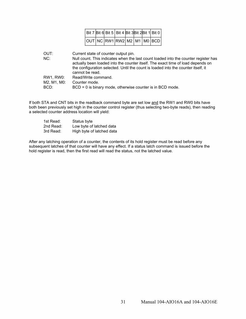
Bit 7 Bit 6 Bit 5 Bit 4 Bit 3Bit 2Bit 1 Bit 0
OUT NC RW1 RW2 M2 M1 M0 BCD
OUT: Current state of counter output pin. NC: Null count. This indicates when the last count loaded into the counter register has
actually been loaded into the counter itself. The exact time of load depends on the configuration selected. Until the count is loaded into the counter itself, it cannot be read.
RW1, RW0: Read/Write command. M2, M1, M0: Counter mode. BCD: BCD = 0 is binary mode, otherwise counter is in BCD mode.
If both STA and CNT bits in the readback command byte are set low and the RW1 and RW0 bits have both been previously set high in the counter control register (thus selecting two-byte reads), then reading a selected counter address location will yield:
1st Read: Status byte 2nd Read: Low byte of latched data 3rd Read: High byte of latched data After any latching operation of a counter, the contents of its hold register must be read before any subsequent latches of that counter will have any effect. If a status latch command is issued before the hold register is read, then the first read will read the status, not the latched value.

Manual 104-AIO16A and 104-AIO16E 32
Appendix B: Calibration This board features digitally controlled potentiometers which are used to adjust the gain and offset of the A/D function and the gain of the DAC function. This allows both the analog inputs and outputs to be calibrated from software in the field. In order to obtain accurate data, the proper values must be loaded into the digital potentiometers each time the board is powered. If no constants are loaded, the potentiometers will power-on to the center of their ranges, which will result in a non- or poorly-calibrated situation. When the board ships from the factory it already has a valid set of calibration constants preloaded into the EEPROM for your immediate use. The various calibration steps are all wrapped up in a calibration program for your use. This program runs in DOS (and compatible environments only) and is written in Borland C/C++ 3.1 with source code provided. You will need a DVM and a calibrated voltage source to run the program. The following steps are only necessary if you are writing your own calibration program, e.g. for a new operating system. If you are unable to run the provided calibration program, it is recommended you examine its source code for details on performing the calibration in your own code. The rest of the chapter is broken down into several sections. First is an overview, a kind of “executive summary” describing the two major steps involved in calibrating the board. Following this is a breakdown of the 5 calibration steps for the DAC. This breakdown is an “engineering summary” providing enough detail that someone very familiar with the board could proceed. Then an in-depth step-by-step walkthrough is provided. Following this is a breakdown of the steps for the ADC. Finally an in-depth step-by-step walkthrough is provided for the ADC. Steps are numbered consistently between the overview, breakdown, and step-by-step sections of this section so you can easily flip between them to build an understanding of the process. Overview: Calibrating without using the provided calibration program This overview applies to both the DAC calibration and ADC calibration. Two parts exist to the calibration process, and understanding these two parts is key to the entire procedure. Step 1. Determine the calibration constants. Step 2. Write the calibration constants into the calibration potentiometers. Step 1 only needs to be performed if the board’s data begins to appear out-of-calibration. A good rule of thumb is to determine new calibration constants every six to twelve months of regular use. If your environment undergoes frequent environmental changes, more frequent calibration may be indicated. When the board ships from the factory it already has a valid set of calibration constants preloaded into the EEPROM for your immediate use. Step 2, writing the calibration constants into the digital calibration potentiometers, must occur each time the board is powered-up (or reset). Typically, each time your program executes you’ll write these values, even if the program was run before.
Manual 104-AIO16A and 104-AIO16E 33
Many devices using digital potentiometers require the software to load the calibration coefficients from a file-on-disk, matching the file to the board based on a manually entered serial number, or some similarly complex method. This board instead contains EEPROM to store the calibration constants. This makes it very simple: the board remembers its own constants, there’s no need for a file on disk, or serial number lookup databases, etc. The details are different between A/D and DAC calibration, and are discussed separately, below. Breakdown: Calibrating the DACs DAC calibration is very simple, and provides a clear introduction to several of the concepts used in calibrating the A/D. The process is designed to evaluate the differences between what you’ve asked the DAC to output and what it really produces. This difference is the amount the board is out of calibration. By adjusting digital potentiometers in the DAC circuit, you reduce this calibration error by successive approximation until it reaches zero. When it is zero, and the board is calibrated, you store the amount of adjustment for later use. First, let’s expand Step 1 mentioned above into its component sub-steps for the DAC: Step 1. Determine the Calibration Constants for the DAC 1.1 Output a value corresponding to a known voltage1 on a DAC 1.2 Measure the output value of the DAC with a DVM 1.3 Adjust the value in the digital calibration potentiometer for that DAC until the voltage read
by the DVM matches the known value being output. 1.4 Store the value from the digital calibration potentiometer into a spot2 in the EEPROM for
use on the next and subsequent board initializations. 1.5 Repeat steps for the other DAC. Step 2. Write the Calibration Constants into the Calibration Potentiometers
For details on Step 2, please refer to section “Step 2" near the end of this appendix. 1: The value corresponding to a known voltage to output depends on the range of the DAC as selected by jumpers on the board. Software can determine the current jumper configured range using the status register at Base + 8 (Chapter 6). 2: The correct spot in EEPROM varies with the DAC number being calibrated, and the currently selected range (see note 1). Please note, you could use any location in the EEPROM you want, as long as you always use the same location. We recommend you use the same locations as our provided Calibration program, drivers, and samples, as shown in Table B-1, following.
Manual 104-AIO16A and 104-AIO16E 34
Step-By-Step: Calibrating the DACs Now let’s describe these steps in detail. 1.1 Output a known value to the DAC. You should determine the maximum range of the DAC using
Base + 12 (see Chapter 5). Pick a value approximately 5% lower than this maximum. By using a value lower than the maximum you avoid calibrating off-the-end of the range. Alternately, choose the voltage most likely to be output by your application in your own use. For example, if you’re going to be using primarily voltages near 6.2 Volts, you may want to calibrate it at that voltage. Just substitute whatever voltage you choose in the math that follows. Output this value to the DAC under calibration. For example, if your DAC is jumpered for the 0-10 Volt output range, a value of 9.5 Volts (95% of 10 Volts) would be a good choice. Convert this voltage to a 12-bit digital count value (Counts = (Volts / MaxVolts) * MaxCounts, so: Counts = (9.5 / 10) * (2^12 - 1) = 0.95 * 4095 = 3890.25. Only a 12-bit integer numbers can be written to the DAC, so we’ll use 3890 as our count value. This equates to F32 hex, which we’ll write to the DAC under calibration. Its important that you are precise when calibrating, so don’t forget about that 0.25 count we threw away. If we run the equation backwards to determine what voltage F32 counts equates to, we don’t get 9.5 volts. Let’s run the math: Volts = (Counts / MaxCounts) * MaxVolts, so Volts = (F32 / FFF) * 10 = 0.9499 * 10 = 9.499 Volts. Not quite 9.5 volts.
1.2 Measure the output value of the DAC with a DVM. Now that we know precisely what output
voltage to expect, connect a DVM to the DAC output pin on P1 (pin 25 or pin 26 for DAC 0 or DAC 1, respectively. Use Pin 24 for ground.) The DVM should be set for DC voltage measurement. Once connected the DVM should read 9.499 Volts, but may not be exactly correct. Remember, if you’re using a different “known output value”, you should see a number near it, not near 9.499.
1.3 Adjust the value in the digital calibration potentiometer for the DAC you’re calibrating until the
reading on the DVM shows your known output value. You adjust this potentiometer’s value using the process described in Base + 19 in Chapter 5. Probably the best way to quickly find the correct value is to initialize the potentiometer with half its maximum value (use 80hex), then increment or decrement the value until the DVM reads accurately.
1.4 Once you’ve determined the value that correctly adjusts the DAC output to match the known
output voltage, store it in the EEPROM for later use. Doing so allows you to re-write the value into the calibration potentiometer on the next board initialization without resorting to storing the values in a reference database or calibration configuration files on a hard disk or floppies, etc. The location into which you store the value varies based on the DAC number you’re calibrating and the range you have selected on the board via jumpers. Consult Table B-1 for a list of the locations the provided Calibration software, samples, and drivers use.
1.5 Repeat these steps for the other DAC. When you’ve finished these steps the DACs are calibrated. The next time the board is reset, only Step 2 needs to be performed. In brief, this involves reading the value out of the correct EEPROM location and writing it to the calibration potentiometer. The details of Step 2 are described near the end of this appendix, following.

Manual 104-AIO16A and 104-AIO16E 35
Breakdown: Calibrating the A/D A/D Calibration, while fundamentally different than the DAC calibration process described above, is also very similar. In the A/D calibration you are determining the amount of calibration error, adjusting the digital potentiometers until the error is eliminated, and storing the adjustment for later use. Unlike the DAC, there are two digital potentiometers for the A/D (offset adjust and gain adjust). The same two steps apply: Step 1. Determine the calibration constants. Step 2. Write the calibration constants into the calibration potentiometers. First, let’s expand Step 1 into its component sub-steps for the A/D: Step 1. Determine the Calibration Constants for the A/D 1.1 Offset Adjust 1.1.1 Apply Ground to the A/D input. 1.1.2 Acquire the voltage using the A/D converter. 1.1.3 Adjust the value in the digital calibration potentiometer for the A/D until the voltage read
by the A/D indicates 1 count1. 1.1.4 Store the value from the digital calibration potentiometer into a spot2 in the EEPROM for
use on the next and subsequent board initializations. 1.2 Gain Adjust 1.2.1 Apply a known voltage3 to the A/D Input. 1.2.2 Acquire the voltage using the A/D converter. 1.2.3 Adjust the value in the digital calibration potentiometer for the A/D until the voltage read
by the A/D matches the input voltage. 1.2.4 Store the value from the digital calibration potentiometer into a spot2 in the EEPROM for
use on the next and subsequent board initializations. Step 2. Write the Calibration Constants into the Calibration Potentiometers
For details on step 2, please refer to the section “Step 2" near the end of this appendix. Note 1: Zero calibration is performed to a value of “1" count instead of “0" to avoid railing the inputs, a condition where you calibrate the board off the end of a range due to the inability of the device to report voltages above the maximum or below the minimum. Note 2: The correct spot in EEPROM varies with the A/D range and single-ended/differential selection being calibrated. We recommend you use the same locations as our provided Calibration program, drivers, and samples, as shown in Table B-1, below. Note 3: The known voltage to use varies with the jumper selected A/D input range. For best results apply a voltage within 5% of the full scale voltage for your selected range.

Manual 104-AIO16A and 104-AIO16E 36
Step-By-Step: Calibrating the A/D Step 1. Determine the Calibration Constants for the A/D 1.1 Offset Adjust 1.1.1 Apply Ground to the A/D input. For best results, all channels should be grounded. Any single
channel would also work. To ground a single channel in single-ended mode, connect its input pin on connector P2 to a ground pin on P2. For example, to ground Channel 0, connect P2 Pin 1 to P2 Pin 3. To “ground” a channel in Differential mode, connect the channel’s pin, and the channel+8's pin together (and preferably to ground.) For example, to “ground” channel 0 in differential mode, connect Channel 0 (P2 Pin 1) to Channel 8 (P2 Pin 2) (and preferably to ground, P2 Pin 3 as well).
1.1.2 Acquire the voltage using the A/D converter. The simplest way is using the Software Mode.
Software mode is described in Chapter 5: Programming. In essence it consists of five steps: Set Channel, Set Gain, Start Conversion, Wait for End of Conversion, Read Data. For calibration purposes the Channel should be whichever channel is grounded. The Channel Scan Limits register at Base +2 should contain only that one channel. Read the data using the EMPTY bit to indicate when data is available. Software gain at Base +4 should be configured for whichever range you’ll actually be using, or the Gain x1 setting. The software gain amplifier is a laser-trimmed part and does not need separate calibration per setting. For optimum results data should be heavily averaged to eliminate any noise from the computations.
1.1.3 Adjust the value in the digital calibration potentiometer for the A/D until the voltage read by the
A/D indicates 1 count. Many methods of determining values for the digital calibration potentiometer exist. One possible method: Set the Pot to “0" and take a reading. If the result is off-scale (reading 0000 or FFFF counts) set the Pot to “FF” and take another reading. One of these two readings will not be “railed” off-scale. Increment or decrement the Pot load value until the data read from the A/D reads 0001. For the most accurate results, continue decrementing or incrementing the Pot until the reading first becomes 0000.
1.1.4 Store the value from the digital calibration potentiometer into a spot in the EEPROM for use on
the next and subsequent board initializations. The correct spot in EEPROM varies with the A/D range and single-ended/differential selection being calibrated. We recommend you use the same locations as our provided Calibration program, drivers, and samples, as shown in Table B-1, below. Write the value using the procedure outlined in the description of Base + 19 in Chapter 5. For example, if calibrating the Offset of the 0-10 Volts Single-Ended setting of the board, we recommend you write the calibration Potentiometer value into the “5" location of the EEPROM.

Manual 104-AIO16A and 104-AIO16E 37
1.2 Gain Adjust 1.2.1 Apply a known voltage to the A/D Input. When adjusting the gain, a known voltage very near the
maximum input of the A/D converter will result in a good reading across the entire range. Alternately, calibrating the A/D to a voltage near the actual application voltage you’ll be expecting in your system results in perfect readings in your specific system. In the vast majority of cases, either calibration method will result in correct data. Continuing our example from above, when calibrating the 0-10V range a voltage near 10 Volts is recommended: we’ll use 9.95 Volts as our Known Voltage. Using a calibrated voltage source apply your known voltage to the inputs of at least one A/D channel. The other channels should not have signals connected, or should be grounded. To connect a known voltage to channel 0, connect the voltage to P2 Pin 1, and use P2 Pin 3 as the reference ground.
1.2.2 Acquire the voltage using the A/D converter. See step 1.1.2 1.2.3 Adjust the value in the digital calibration potentiometer for the A/D until the voltage read by the
A/D matches the input voltage. Many methods of determining values for the digital calibration potentiometer exist. One possible method: Set the Pot to “0" and take a reading. If the result is off-scale (reading 0000 or FFFF counts) set the Pot to “FF” and take another reading. One of these two readings will not be “railed” off-scale. Increment or decrement the Pot load value until the data read from the A/D reads the Known Voltage. To convert from counts to voltage use the following equation: Volts=Span*Counts/MaxCounts-Offset. MaxCounts on a 16-bit A/D is 65536, and Span and Offset vary with the selected range. In any unipolar range, Offset is zero, and the Span is equal to the maximum voltage. In any bipolar range the Span is equal to the maximum input voltage minus the minimum input voltage, and Offset is half of this value. For example, ±5Volt range has a Span of 10V and an Offset of 5V. If the A/D reads FFE9 counts on a 0-10V range, the voltage being indicated is 10*FAE9/FFFF-0, or 9.801 Volts.
1.2.4 Store the value from the digital calibration potentiometer into a spot in the EEPROM for use on
the next and subsequent board initializations. The correct spot in EEPROM varies with the A/D range and single-ended/differential selection being calibrated. We recommend you use the same locations as our provided Calibration program, drivers, and samples, as shown in Table B-1, below. Write the value using the procedure outlined in the description of Base + 19 in Chapter 5. For example, if calibrating the Gain of the 0-10 Volts Single-Ended setting of the board, we recommend you write the calibration potentiometer value into the “D" location of the EEPROM.
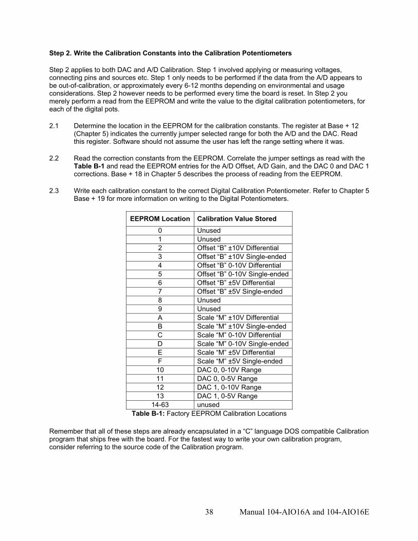
Manual 104-AIO16A and 104-AIO16E 38
Step 2. Write the Calibration Constants into the Calibration Potentiometers Step 2 applies to both DAC and A/D Calibration. Step 1 involved applying or measuring voltages, connecting pins and sources etc. Step 1 only needs to be performed if the data from the A/D appears to be out-of-calibration, or approximately every 6-12 months depending on environmental and usage considerations. Step 2 however needs to be performed every time the board is reset. In Step 2 you merely perform a read from the EEPROM and write the value to the digital calibration potentiometers, for each of the digital pots. 2.1 Determine the location in the EEPROM for the calibration constants. The register at Base + 12
(Chapter 5) indicates the currently jumper selected range for both the A/D and the DAC. Read this register. Software should not assume the user has left the range setting where it was.
2.2 Read the correction constants from the EEPROM. Correlate the jumper settings as read with the
Table B-1 and read the EEPROM entries for the A/D Offset, A/D Gain, and the DAC 0 and DAC 1 corrections. Base + 18 in Chapter 5 describes the process of reading from the EEPROM.
2.3 Write each calibration constant to the correct Digital Calibration Potentiometer. Refer to Chapter 5
Base + 19 for more information on writing to the Digital Potentiometers.
EEPROM Location Calibration Value Stored 0 Unused 1 Unused 2 Offset “B” ±10V Differential 3 Offset “B” ±10V Single-ended 4 Offset “B” 0-10V Differential 5 Offset “B” 0-10V Single-ended6 Offset “B” ±5V Differential 7 Offset “B” ±5V Single-ended 8 Unused 9 Unused A Scale “M” ±10V Differential B Scale “M” ±10V Single-ended C Scale “M” 0-10V Differential D Scale “M” 0-10V Single-endedE Scale “M” ±5V Differential F Scale “M” ±5V Single-ended 10 DAC 0, 0-10V Range 11 DAC 0, 0-5V Range 12 DAC 1, 0-10V Range 13 DAC 1, 0-5V Range
14-63 unused Table B-1: Factory EEPROM Calibration Locations
Remember that all of these steps are already encapsulated in a “C” language DOS compatible Calibration program that ships free with the board. For the fastest way to write your own calibration program, consider referring to the source code of the Calibration program.

Manual 104-AIO16A and 104-AIO16E 39
Customer Comments
If you experience any problems with this manual or just want to give us some feedback, please email us at: [email protected]. Please detail any errors you find and include your mailing address so that we can send you any manual updates.
10623 Roselle Street, San Diego CA 92121
Tel. (858)550-9559 FAX (858)550-7322 www.accesio.com