1022 IEEE TRANSACTIONS ON MICROWAVE …dl.edatop.com/mte/ansoft/edatop.com_Investigation of a...1022...
10
1022 IEEE TRANSACTIONS ON MICROWAVE THEORY AND TECHNIQUES, VOL. 58, NO. 4, APRIL 2010 Investigation of a Wideband 90 Hybrid Coupler With an Arbitrary Coupling Level Leung Chiu, Member, IEEE, and Quan Xue, Senior Member, IEEE Abstract—This paper presents a new class of wideband 90 hy- brid coupler with an arbitrary coupling level. The physical size of the proposed coupler is close to that of a conventional two-section branch-line coupler, but it has an additional phase inverter. The impedance bandwidth of the proposed coupler is close to that of a four-section branch-line coupler. The proposed coupler is a backward-wave coupler with a port assignment different from that of a conventional branch-line coupler. The design formulas of the proposed coupler are proved based on its even- and odd-mode half structures. We demonstrated three couplers at the center frequency of 2 GHz with different design parameters. Index Terms—Bandwidth enhancement, 90 hybrid coupler, parallel-strip phase inverter. I. INTRODUCTION R ECENTLY, some kinds of (double-sided) parallel-strip circuits have been proposed [1]–[8]. The parallel-strip line is a kind of balanced transmission line with a piece of dielectric substrate sandwiched between two conductor strips. Parallel-strip lines can be employed for RF and microwave ap- plications and have the advantages of a balanced transmission line, a wide range of characteristic impedance, simple transi- tion with other transmission lines and lumped elements, and a phase inverter. In our research group, various designs making use of those unique properties were proposed, such as balanced devices [1], [2], filters [3], [4], and power dividers [5], [6]. A parallel-strip phase inverter is an especially useful technique for introducing a 180 phase delay without increasing the trans- mission line length, using the via hole to connect the signal of one line to the ground of the other, and vice versa, effectively swapping the signal and ground lines at the junction. It has been of particular interest to the designs of compact and wideband 180 hybrid couplers [7]. Power dividers achieving enhanced port-to-port isolation and wideband bandpass filters employing phase inverter are reported in [6] and [3], respectively. The de- tails of the geometry and the lumped circuit model of the par- allel-strip phase inverter are reported in [6]. Manuscript received July 17, 2009; revised December 28, 2009. First pub- lished March 15, 2010; current version published April 14, 2010. This work was supported in part by the Research Grants Council of Hong Kong SAR, China, under Grant CityU7002354. L. Chiu is with the State Key Laboratory of Millimeter Waves, School of Information Science and Engineering, Southeast University, Nanjing 210096, China (e-mail: [email protected]). Q. Xue is with the State Key Laboratory of Millimeter Waves, City University of Hong Kong, Kowloon, Hong Kong (e-mail: [email protected]). Color versions of one or more of the figures in this paper are available online at http://ieeexplore.ieee.org. Digital Object Identifier 10.1109/TMTT.2010.2042835 Fig. 1. Schematic diagrams of proposed 90 hybrid coupler with various schemes. Directional couplers with either 90 or 180 phase shifts are the critical circuit elements of all wireless communications sys- tems. Generally, the critical design issues for a directional cou- pler include: 1) impedance bandwidth; 2) port-to-port isolation; 3) magnitude imbalance; and 4) phase imbalance. In partic- ular, 90 hybrid couplers such as the branch-line coupler, the Lange-line coupler, and the coupled-line coupler are extensively studied and utilized in various RF and microwave systems. They function as power combiner/dividers with a 90 phase shift, and they are particularly useful in many components such as bal- anced or Doherty amplifiers, balanced mixers, and antenna- or array-fed networks. A wideband parallel-strip 90 hybrid coupler using a phase inverter was originally proposed in [8], and its schematic dia- gram is shown in Fig. 1(a). The physical size of the proposed de- sign is close to a conventional two-section branch-line coupler, but its performance in terms of the above four design issues is similar to that of a four-section branch-line coupler. In fact, two different designs with exactly the same theoretical performance are shown in Fig. 1(b) and (c). The single phase inverter design shown in Fig. 1(a) is chosen because the phase inverter discon- tinuities always degrade the coupler performance and it is easier to analyze compared with the designs shown in Fig. 1(b) and (c). 0018-9480/$26.00 © 2010 IEEE Authorized licensed use limited to: CityU. Downloaded on April 28,2010 at 08:07:33 UTC from IEEE Xplore. Restrictions apply.
Transcript of 1022 IEEE TRANSACTIONS ON MICROWAVE …dl.edatop.com/mte/ansoft/edatop.com_Investigation of a...1022...
1022 IEEE TRANSACTIONS ON MICROWAVE THEORY AND TECHNIQUES, VOL. 58, NO. 4, APRIL 2010
Investigation of a Wideband 90 Hybrid CouplerWith an Arbitrary Coupling Level
Leung Chiu, Member, IEEE, and Quan Xue, Senior Member, IEEE
Abstract—This paper presents a new class of wideband 90 hy-brid coupler with an arbitrary coupling level. The physical size ofthe proposed coupler is close to that of a conventional two-sectionbranch-line coupler, but it has an additional phase inverter. Theimpedance bandwidth of the proposed coupler is close to thatof a four-section branch-line coupler. The proposed coupler is abackward-wave coupler with a port assignment different fromthat of a conventional branch-line coupler. The design formulas ofthe proposed coupler are proved based on its even- and odd-modehalf structures. We demonstrated three couplers at the centerfrequency of 2 GHz with different design parameters.
Index Terms—Bandwidth enhancement, 90 hybrid coupler,parallel-strip phase inverter.
I. INTRODUCTION
R ECENTLY, some kinds of (double-sided) parallel-stripcircuits have been proposed [1]–[8]. The parallel-strip
line is a kind of balanced transmission line with a piece ofdielectric substrate sandwiched between two conductor strips.Parallel-strip lines can be employed for RF and microwave ap-plications and have the advantages of a balanced transmissionline, a wide range of characteristic impedance, simple transi-tion with other transmission lines and lumped elements, and aphase inverter. In our research group, various designs makinguse of those unique properties were proposed, such as balanceddevices [1], [2], filters [3], [4], and power dividers [5], [6]. Aparallel-strip phase inverter is an especially useful techniquefor introducing a 180 phase delay without increasing the trans-mission line length, using the via hole to connect the signal ofone line to the ground of the other, and vice versa, effectivelyswapping the signal and ground lines at the junction. It has beenof particular interest to the designs of compact and wideband180 hybrid couplers [7]. Power dividers achieving enhancedport-to-port isolation and wideband bandpass filters employingphase inverter are reported in [6] and [3], respectively. The de-tails of the geometry and the lumped circuit model of the par-allel-strip phase inverter are reported in [6].
Manuscript received July 17, 2009; revised December 28, 2009. First pub-lished March 15, 2010; current version published April 14, 2010. This work wassupported in part by the Research Grants Council of Hong Kong SAR, China,under Grant CityU7002354.
L. Chiu is with the State Key Laboratory of Millimeter Waves, School ofInformation Science and Engineering, Southeast University, Nanjing 210096,China (e-mail: [email protected]).
Q. Xue is with the State Key Laboratory of Millimeter Waves, City Universityof Hong Kong, Kowloon, Hong Kong (e-mail: [email protected]).
Color versions of one or more of the figures in this paper are available onlineat http://ieeexplore.ieee.org.
Digital Object Identifier 10.1109/TMTT.2010.2042835
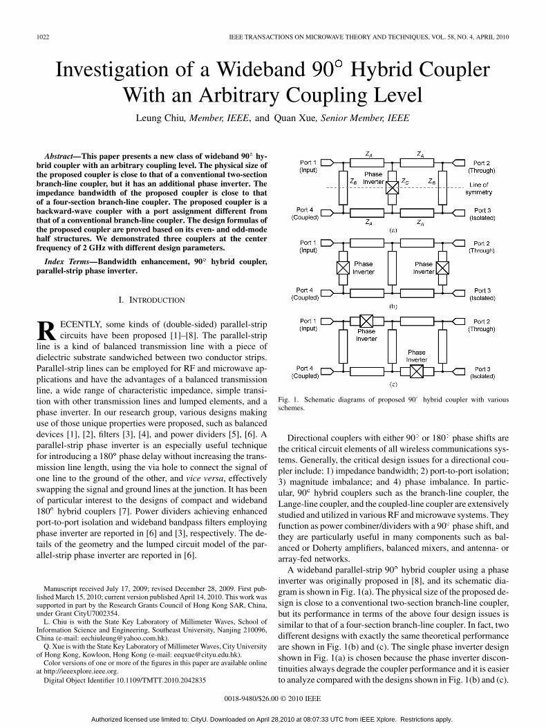
Fig. 1. Schematic diagrams of proposed 90 hybrid coupler with variousschemes.
Directional couplers with either 90 or 180 phase shifts arethe critical circuit elements of all wireless communications sys-tems. Generally, the critical design issues for a directional cou-pler include: 1) impedance bandwidth; 2) port-to-port isolation;3) magnitude imbalance; and 4) phase imbalance. In partic-ular, 90 hybrid couplers such as the branch-line coupler, theLange-line coupler, and the coupled-line coupler are extensivelystudied and utilized in various RF and microwave systems. Theyfunction as power combiner/dividers with a 90 phase shift, andthey are particularly useful in many components such as bal-anced or Doherty amplifiers, balanced mixers, and antenna- orarray-fed networks.
A wideband parallel-strip 90 hybrid coupler using a phaseinverter was originally proposed in [8], and its schematic dia-gram is shown in Fig. 1(a). The physical size of the proposed de-sign is close to a conventional two-section branch-line coupler,but its performance in terms of the above four design issues issimilar to that of a four-section branch-line coupler. In fact, twodifferent designs with exactly the same theoretical performanceare shown in Fig. 1(b) and (c). The single phase inverter designshown in Fig. 1(a) is chosen because the phase inverter discon-tinuities always degrade the coupler performance and it is easierto analyze compared with the designs shown in Fig. 1(b) and (c).
0018-9480/$26.00 © 2010 IEEE
Authorized licensed use limited to: CityU. Downloaded on April 28,2010 at 08:07:33 UTC from IEEE Xplore. Restrictions apply.
CHIU AND XUE: INVESTIGATION OF WIDEBAND 90 HYBRID COUPLER WITH ARBITRARY COUPLING LEVEL 1023
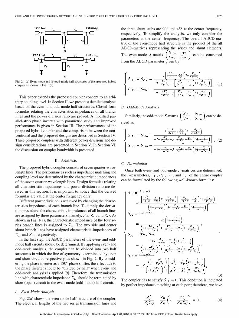
Fig. 2. (a) Even-mode and (b) odd-mode half structures of the proposed hybridcoupler as shown in Fig. 1(a).
This paper extends the proposed coupler concept to an arbi-trary coupling level. In Section II, we present a detailed analysisbased on the even- and odd-mode half structures. Closed-formformulas relating the characteristics impedances of all branchlines and the power division ratio are proved. A modified par-allel-strip phase inverter with parametric study and improvedperformance is given in Section III. The performances of theproposed hybrid coupler and the comparison between the con-ventional and the proposed designs are described in Section IV.Three proposed couplers with different power divisions and de-sign considerations are presented in Section V. In Section VI,the discussion on coupler bandwidth is presented.
II. ANALYSIS
The proposed hybrid coupler consists of seven quarter-wave-length lines. The performances such as impedance matching andcoupling level are determined by the characteristic impedancesof the seven quarter-wavelength lines. Design formulas relatingall characteristic impedances and power division ratio are de-rived in this section. It is important to notice that the derivedformulas are valid at the center frequency only.
Different power division is achieved by changing the charac-teristics impedance of each branch line. To simply the deriva-tion procedure, the characteristic impedances of all branch linesare assigned by three parameters, namely, , , and . Asshown in Fig. 1(a), the characteristic impedance of the four se-ries branch lines is assigned to . The two side and centershunt branch lines have assigned characteristic impedances of
and , respectively.In the first step, the ABCD parameters of the even- and odd-
mode half circuits should be determined. By applying even- andodd-mode analysis, the coupler can be divided into two halfstructures in which the line of symmetry is terminated by openand short circuits, respectively, as shown in Fig. 2. By consid-ering the phase inverter as a 180 phase shifter, the effect due tothe phase inverter should be “divided by half” when even- andodd-mode analysis is applied [9]. Therefore, the transmissionline with characteristic impedance should be terminated byshort (open) circuit in the even-mode (odd-mode) half circuit.
A. Even-Mode Analysis
Fig. 2(a) shows the even-mode half structure of the coupler.The electrical lengths of the two series transmission lines and
the three shunt stubs are 90 and 45 at the center frequency,respectively. To simplify the analysis, we only consider theparameters at the center frequency. The overall ABCD-ma-trix of the even-mode half structure is the product of the allABCD-matrices representing the series and shunt elements.
The even-mode -matrix can be conversed
from the ABCD parameter given by
(1)
B. Odd-Mode Analysis
Similarly, the odd-mode -matrix can be de-
rived as
(2)
C. Formulation
Once both even- and odd-mode -matrices are determined,the -parameters, , , , and of the entire couplercan be formulated by the following well-known formulas:
(3)The coupler has to satisfy . This condition is indicatedby perfect impedance matching at each port; therefore, we have
(4)
Authorized licensed use limited to: CityU. Downloaded on April 28,2010 at 08:07:33 UTC from IEEE Xplore. Restrictions apply.
1024 IEEE TRANSACTIONS ON MICROWAVE THEORY AND TECHNIQUES, VOL. 58, NO. 4, APRIL 2010
Substituting (4) into (3), we have
(5)
We can observe three issues about the proposed coupler from(5). First, implies that port 3 is the isolated port ifport 1 is assigned as the input port. Second, the phase differencebetween the signals at the through port (port 2) and coupledport (port 4) is exactly 90 , where , , , and arepositive and purely real numbers. Third, the power division ratio
, which is defined as the ratio of signal power at the throughport to that at coupled port, is a function of and . canbe expressed as
(6)
By solving (4) and (6), we can get the circuit parameters ,, and as the functions of and , hence we have
(7)
(8)
The value of is unique for a given , while the values ofand are not unique. For a given power division ratio,
we will have high degree of freedom of choosing the values ofthe circuit parameters and if both and satisfy(8). Perfect impedance matching and port-to-port isolation isalways achieved at the center frequency with different frequencyresponses if a different set of and is chosen.
The series branch lines are connected to the four ports. It canslightly reduce the discontinuity at the four T-junctions if thevalue of is assigned to same as the port impedance. We have
(9)
All of the designed couplers in this paper will be based on (9).For the case of , we will have discussion in the Ap-pendix. Therefore, becomes unique and can be expressed as
(10)
Substituting (7), (9), and (10) into (5), the scattering matrix ofthe proposed coupler at the center frequency can be representedas follows:
(11)
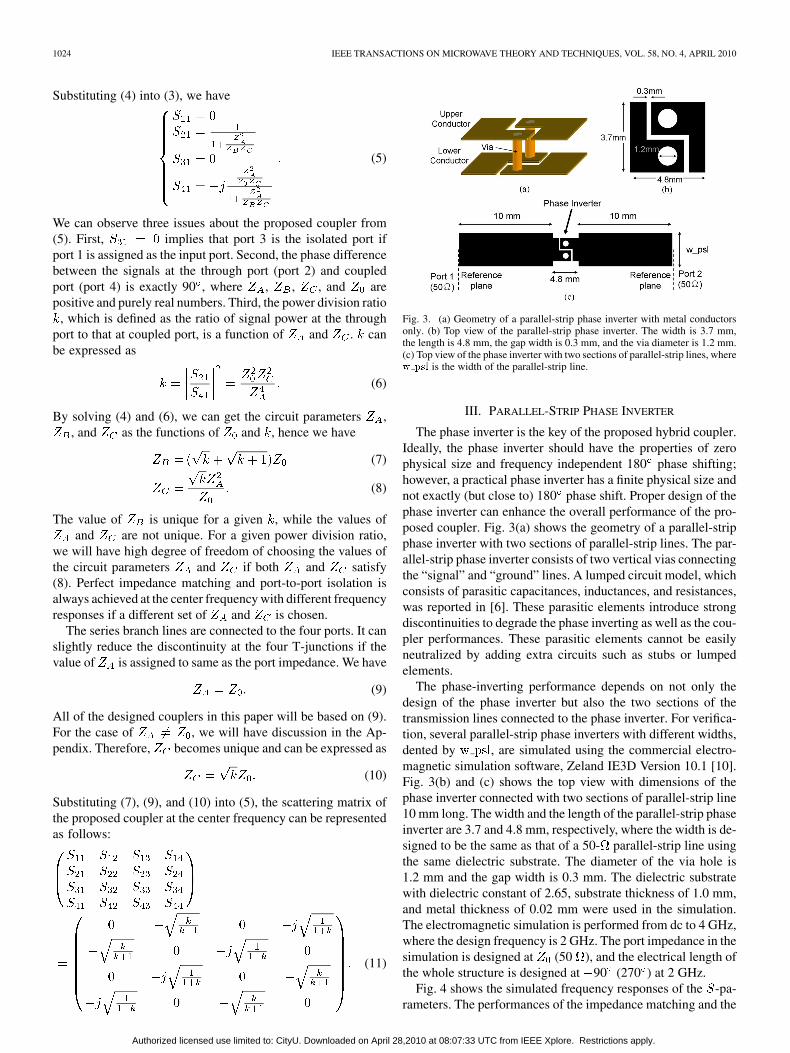
Fig. 3. (a) Geometry of a parallel-strip phase inverter with metal conductorsonly. (b) Top view of the parallel-strip phase inverter. The width is 3.7 mm,the length is 4.8 mm, the gap width is 0.3 mm, and the via diameter is 1.2 mm.(c) Top view of the phase inverter with two sections of parallel-strip lines, where� ��� is the width of the parallel-strip line.
III. PARALLEL-STRIP PHASE INVERTER
The phase inverter is the key of the proposed hybrid coupler.Ideally, the phase inverter should have the properties of zerophysical size and frequency independent 180 phase shifting;however, a practical phase inverter has a finite physical size andnot exactly (but close to) 180 phase shift. Proper design of thephase inverter can enhance the overall performance of the pro-posed coupler. Fig. 3(a) shows the geometry of a parallel-stripphase inverter with two sections of parallel-strip lines. The par-allel-strip phase inverter consists of two vertical vias connectingthe “signal” and “ground” lines. A lumped circuit model, whichconsists of parasitic capacitances, inductances, and resistances,was reported in [6]. These parasitic elements introduce strongdiscontinuities to degrade the phase inverting as well as the cou-pler performances. These parasitic elements cannot be easilyneutralized by adding extra circuits such as stubs or lumpedelements.
The phase-inverting performance depends on not only thedesign of the phase inverter but also the two sections of thetransmission lines connected to the phase inverter. For verifica-tion, several parallel-strip phase inverters with different widths,dented by , are simulated using the commercial electro-magnetic simulation software, Zeland IE3D Version 10.1 [10].Fig. 3(b) and (c) shows the top view with dimensions of thephase inverter connected with two sections of parallel-strip line10 mm long. The width and the length of the parallel-strip phaseinverter are 3.7 and 4.8 mm, respectively, where the width is de-signed to be the same as that of a 50- parallel-strip line usingthe same dielectric substrate. The diameter of the via hole is1.2 mm and the gap width is 0.3 mm. The dielectric substratewith dielectric constant of 2.65, substrate thickness of 1.0 mm,and metal thickness of 0.02 mm were used in the simulation.The electromagnetic simulation is performed from dc to 4 GHz,where the design frequency is 2 GHz. The port impedance in thesimulation is designed at (50 ), and the electrical length ofthe whole structure is designed at 90 (270 ) at 2 GHz.
Fig. 4 shows the simulated frequency responses of the -pa-rameters. The performances of the impedance matching and the
Authorized licensed use limited to: CityU. Downloaded on April 28,2010 at 08:07:33 UTC from IEEE Xplore. Restrictions apply.
CHIU AND XUE: INVESTIGATION OF WIDEBAND 90 HYBRID COUPLER WITH ARBITRARY COUPLING LEVEL 1025
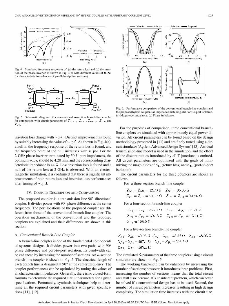
Fig. 4. Simulated frequency responses of: (a) the return loss and (b) the inser-tion of the phase inverter as shown in Fig. 3(c) with different values of � ���
(or characteristic impedances of parallel-strip line sections).
Fig. 5. Schematic diagram of a conventional �-section branch-line couplerfor comparison with circuit parameters of � � � � �� , � � � � �� , and� .
insertion loss change with . Distinct improvement is foundby suitably increasing the value of . As shown in Fig. 4(a),a null in the frequency response of the return loss is found, andthe frequency point of the null increases with . For the2-GHz phase inverter terminated by 50- port impedances, theoptimum should be 4.20 mm, and the corresponding char-acteristic impedance is 44 . Less insertion loss is found and anull of the return loss at 2 GHz is observed. With an electro-magnetic simulation, it is confirmed that there is significant im-provements of both return loss and insertion loss performancesafter tuning of .
IV. COUPLER DESCRIPTION AND COMPARISON
The proposed coupler is a transmission-line 90 directionalcoupler. It divides power with 90 phase difference at the centerfrequency. The port locations of the proposed coupler are dif-ferent from those of the conventional branch-line coupler. Theoperation mechanisms of the conventional and the proposedcouplers are explained and their differences are shown in thissection.
A. Conventional Branch-Line Coupler
A branch-line coupler is one of the fundamental componentsof systems designs. It divides power into two paths with 90phase difference and port-to-port isolation. Its bandwidth canbe enhanced by increasing the number of sections. An -sectionbranch-line coupler is shown in Fig. 5. The electrical length ofeach branch line is designed at 90 at the center frequency. Thecoupler performances can be optimized by tuning the values ofall characteristic impedances. Generally, there is no closed-formformula to determine the required circuit parameters for a givenspecifications. Fortunately, synthesis techniques help to deter-mine all the required circuit parameters with given specifica-tions [11], [12].
Fig. 6. Performance comparison of the conventional branch-line couplers andthe proposed hybrid coupler. (a) Impedance matching. (b) Port-to-port isolation.(c) Magnitude imbalance. (d) Phase imbalance.
For the purposes of comparison, three conventional branch-line couplers are simulated with approximately equal power di-vision. All circuit parameters can be found based on the designmethodology presented in [11] and are finely tuned using a cir-cuit simulator (Agilent Advanced Design System) [13]. An idealtransmission-line model is used in the simulation, and the effectof the discontinuities introduced by all T-junctions is omitted.All circuit parameters are optimized with the goals of mini-mizing the magnitudes of (return loss) and (port-to-portisolation).
The circuit parameters for the three couplers are shown asfollows.
For a three-section branch-line coupler
For a four-section branch-line coupler
For a five-section branch-line coupler
The simulated -parameters of the three couplers using a circuitsimulator are shown in Fig. 5.
The working bandwidth can be enhanced by increasing thenumber of sections; however, it introduces three problems. First,increasing the number of sections means that the total circuitarea will also increase. It is an inherent problem, which can neverbe solved if a conventional design has to be used. Second, thenumber of circuit parameters increases resulting in high designcomplexity. The simulation time increases with the circuit size.
Authorized licensed use limited to: CityU. Downloaded on April 28,2010 at 08:07:33 UTC from IEEE Xplore. Restrictions apply.
1026 IEEE TRANSACTIONS ON MICROWAVE THEORY AND TECHNIQUES, VOL. 58, NO. 4, APRIL 2010
Third, it always results in very high characteristic impedancetransmission lines, which are implemented by very narrow lines.The narrow lines lead to a difficulty in fabrication, increasing therelative fabrication errors, and reducing the power handling. Forexample, the transmission lines with characteristic impedance
in the five-section coupler are extremelydifficult to be realized by standard printed circuit board fabri-cation technology. These are the main reasons why the numberof sections is limited to four or five. To solve this problem, theslotted ground technique [14] and offset parallel-strip lines [6]have been proposed to realize the high characteristic impedanceline easily; therefore, a multisection branch-line coupler withoutvery narrow lines was proposed. The number of sections islimited to four or five if the conventional branch-line coupler hasequal power division using standard printed circuit board (PCB)fabrication technology.
B. Proposed Coupler
A circuit model of the proposed hybrid coupler with the fol-lowing circuit parameters was built in circuit simulator for com-parison:
Similarly, ideal transmission-line and phase-inverter models areused in the simulation. In addition, the effect of the discontinu-ities introduced by all T-junctions is neglected. The simulated
-parameters of the proposed coupler are shown in Fig. 5. Itis found that the proposed coupler achieves relative impedancebandwidth of about 96%, which is between that of four-sectionand five-section branch-line couplers if 10-dB return loss isthe reference. Besides, there is one null in the frequency re-sponses of both return loss and port-to-port isolation, whilenulls can be found in that of the optimized -section branch-linecoupler.
The behavior of the backward-wave coupling can be analyt-ically proven by the following expressions, which come fromsubstituting (4) into (1) and (2):
(12)
It has been proven that the proposed branch-line coupler witha phase inverter is a backward-wave coupler, contrary to theconventional one which is a forward-wave coupler, if all portimpedances are matched [15].
V. COUPLER WITH AN ARBITRARY COUPLING LEVEL
A. Parallel-Strip-Line-to-Microstrip-Line Transition
A common SMA connector is used to connect unbalancedtransmission lines such as microstrip line and coplanar wave-guide, while the parallel-strip line is balanced on differentialtransmission lines. In this paper, a linearly tapered microstrip-line-to-parallel-strip-line transition is used for the measurementpurpose. By removing part of the ground plane of the microstripline, the field distribution in the 50- microstrip line gradually
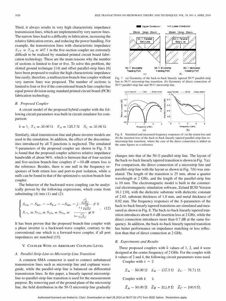
Fig. 7. (a) Geometry of the back-to-back linearly tapered 50-� parallel-stripline to 50-� microstrip-line transition. (b) Geometry of direct connection of50-� parallel-strip line and 50-� microstrip line.
Fig. 8. Simulated and measured frequency responses of: (a) the return loss and(b) the insertion loss of the back-to-back linearly tapered parallel-strip-line-to-microstrip-line transition, where the case of the direct connection is added onthe same figures as a reference.
changes into that of the 50- parallel-strip line. The layout ofthe back-to-back linearly tapered transition is shown in Fig. 7(a).For comparison, the direct connection of a microstrip line andparallel-strip line with the layout as shown in Fig. 7(b) was sim-ulated. The length of the transition is 25 mm, about a quarterwavelength at 2 GHz, and the length of the parallel-strip lineis 10 mm. The electromagnetic model is built in the commer-cial electromagnetic simulation software, Zeland IE3D Version10.1 [10], with the dielectric substrate with dielectric constantof 2.65, substrate thickness of 1.0 mm, and metal thickness of0.02 mm. The frequency responses of the -parameters of theback-to-back linearly tapered transitions are simulated and mea-sured as shown in Fig. 8. The back-to-back linearly tapered tran-sition introduces about 0.4-dB insertion loss at 2 GHz, while thedirect connection introduces more than 0.7 dB at the same fre-quency. In addition, the back-to-back linearly tapered transitionhas better performance on impedance matching or less reflec-tion than that of direct connection at 2 GHz.
B. Experiments and Results
Three proposed couplers with values of 1, 2, and 4 weredesigned at the center frequency of 2 GHz. For the coupler with
values of 2 and 4, the following circuit parameters were used.Coupler with
Coupler with
Authorized licensed use limited to: CityU. Downloaded on April 28,2010 at 08:07:33 UTC from IEEE Xplore. Restrictions apply.

CHIU AND XUE: INVESTIGATION OF WIDEBAND 90 HYBRID COUPLER WITH ARBITRARY COUPLING LEVEL 1027
Fig. 9. Simulated and measured frequency responses of the proposed couplers with different values of �. Magnitude of �-parameters with: (a) � � �, (b) � � �,and (c) � � �. Phase differences with through and coupled ports with: (d) � � �, (e) � � �, and (f) � � �.
All couplers were fabricated on the same dielectric substratewith dielectric constant of 2.65, substrate thickness of 1.0 mm,and metal thickness of 0.02 mm by a standard printed circuitboard fabrication technique. All dimensions of the coupler werefinely tuned by using electromagnetic simulation software (Ze-land IE3D Version 10.1) [10] to take into account the effect ofthe discontinuities introduced by all T-junctions and the phaseinverter. The -parameters of all couplers were measured by anetwork analyzer. Fig. 9 shows that simulated and measured re-sults of the three fabricated couplers. The three fabricated cou-plers have relative impedance bandwidth of about 98%. Withthis bandwidth, all couplers achieve more than 20-dB port-to-port isolation and 90 phase difference between the coupled andthrough ports with less than 2 phase error. Good agreement be-tween the simulation and the measurement is achieved.
C. Design Consideration
For most of the practical applications, a hybrid couplershould be designed to work within a frequency band. Thedesign specification should include both acceptable magnitudeand phase imbalances within certain bandwidth. By properchoosing value of , the overall bandwidth of the proposedcoupler can be widened. It is always preferred that the couplerhas wider overall bandwidth as possible.
This issue is discussed by starting an example. We need todesign a coupler with a specification of equal power divisionwith no more than 1-dB magnitude imbalance and not more than5 phase imbalance.
Normally, if 0 dB is chosen, the circuitparameters are given as follows:
Fig. 10. Simulated frequency responses of the �� � and �� � with: (a) � � �
(0 dB) and (b) � � ������ (�1 dB).
Fig. 10(a) shows the simulated -parameters of the coupler withthe above parameters. The simulated bandwidths of impedancematching, 1-dB magnitude imbalance, and 5 phase imbalanceare 97.80%, 48.20%, and 105.6%, respectively. Therefore, theoverall working bandwidth under the required specificationshould be 48.20%.
It is critical to point out that it is not necessary to achieve 0-dBmagnitude imbalance at the center frequency. As observed fromFig. 10(b), the value of varies with frequency where attendsminimum at the center frequency. From the specification, theminimum acceptable values should be 0.7943
1 dB . If is chosen, the circuit parameters are asfollows:
Fig. 10(b) shows the simulated -parameters of the couplerwith the above parameters. The simulated bandwidths of
Authorized licensed use limited to: CityU. Downloaded on April 28,2010 at 08:07:33 UTC from IEEE Xplore. Restrictions apply.
1028 IEEE TRANSACTIONS ON MICROWAVE THEORY AND TECHNIQUES, VOL. 58, NO. 4, APRIL 2010
Fig. 11. Simulated relationship of the relative bandwidth and parameter � with different values of �. (a) Impedance bandwidth with �� � � �10 dB. (b)Bandwidth with magnitude imbalance bandwidth with �� �� � �0.1 dB. (c) Isolation bandwidth with �� � � �20 dB. (d) Phase imbalance bandwidthwith � � � � � � .
impedance matching, 1-dB magnitude imbalance, and 5 phaseimbalance are 97.40%, 65.80%, and 105.6%, respectively.Hence, the overall working bandwidth under the same spec-ification should be 65.80%. The simulation shows that thecoupler using the second set of circuit parameters results inwider overall bandwidth than that using first set. By assigningthe minimum acceptable value of for a given specification,the coupler can achieve more bandwidth.
VI. DISCUSSION ON COUPLER BANDWIDTH
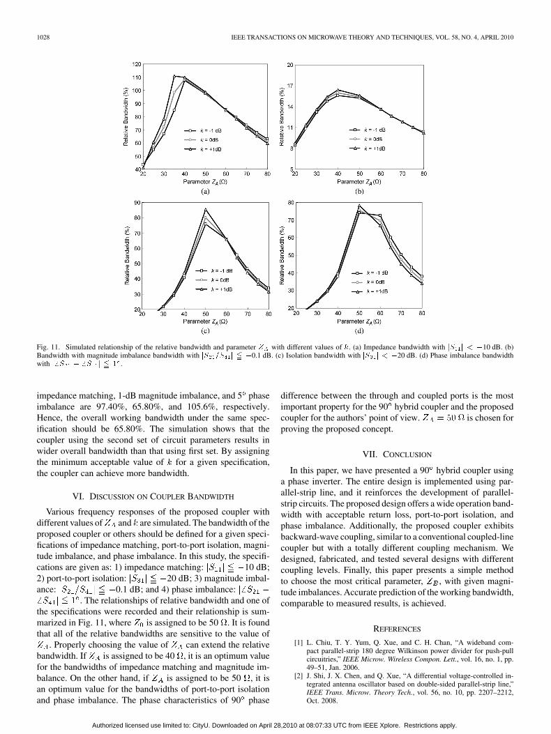
Various frequency responses of the proposed coupler withdifferent values of and are simulated. The bandwidth of theproposed coupler or others should be defined for a given speci-fications of impedance matching, port-to-port isolation, magni-tude imbalance, and phase imbalance. In this study, the specifi-cations are given as: 1) impedance matching: 10 dB;2) port-to-port isolation: 20 dB; 3) magnitude imbal-ance: 0.1 dB; and 4) phase imbalance:
. The relationships of relative bandwidth and one ofthe specifications were recorded and their relationship is sum-marized in Fig. 11, where is assigned to be 50 . It is foundthat all of the relative bandwidths are sensitive to the value of
. Properly choosing the value of can extend the relativebandwidth. If is assigned to be 40 , it is an optimum valuefor the bandwidths of impedance matching and magnitude im-balance. On the other hand, if is assigned to be 50 , it isan optimum value for the bandwidths of port-to-port isolationand phase imbalance. The phase characteristics of 90 phase
difference between the through and coupled ports is the mostimportant property for the 90 hybrid coupler and the proposedcoupler for the authors’ point of view. is chosen forproving the proposed concept.
VII. CONCLUSION
In this paper, we have presented a 90 hybrid coupler usinga phase inverter. The entire design is implemented using par-allel-strip line, and it reinforces the development of parallel-strip circuits. The proposed design offers a wide operation band-width with acceptable return loss, port-to-port isolation, andphase imbalance. Additionally, the proposed coupler exhibitsbackward-wave coupling, similar to a conventional coupled-linecoupler but with a totally different coupling mechanism. Wedesigned, fabricated, and tested several designs with differentcoupling levels. Finally, this paper presents a simple methodto choose the most critical parameter, , with given magni-tude imbalances. Accurate prediction of the working bandwidth,comparable to measured results, is achieved.
REFERENCES
[1] L. Chiu, T. Y. Yum, Q. Xue, and C. H. Chan, “A wideband com-pact parallel-strip 180 degree Wilkinson power divider for push-pullcircuitries,” IEEE Microw. Wireless Compon. Lett., vol. 16, no. 1, pp.49–51, Jan. 2006.
[2] J. Shi, J. X. Chen, and Q. Xue, “A differential voltage-controlled in-tegrated antenna oscillator based on double-sided parallel-strip line,”IEEE Trans. Microw. Theory Tech., vol. 56, no. 10, pp. 2207–2212,Oct. 2008.
Authorized licensed use limited to: CityU. Downloaded on April 28,2010 at 08:07:33 UTC from IEEE Xplore. Restrictions apply.

CHIU AND XUE: INVESTIGATION OF WIDEBAND 90 HYBRID COUPLER WITH ARBITRARY COUPLING LEVEL 1029
[3] K. W. Wong, L. Chiu, and Q. Xue, “Wideband parallel-strip bandpassfilter using phase inverter,” IEEE Microw. Wireless Compon. Lett., vol.18, no. 8, pp. 503–505, Aug. 2008.
[4] J. X. Chen, C. H. K. Chin, and Q. Xue, “Double-sided parallel-stripline with an inserted conductor plane and its applications,” IEEE Trans.Microw. Theory Tech., vol. 55, no. 9, pp. 1899–1904, Sep. 2007.
[5] T. Yang, J. X. Chen, and Q. Xue, “Three-way out-of-phase power di-vider,” Electron. Lett., vol. 44, no. 7, pp. 482–483, Mar. 2008.
[6] L. Chiu and Q. Xue, “A parallel-strip ring power divider with high iso-lation and arbitrary power-dividing ratio,” IEEE Trans. Microw. TheoryTech., vol. 55, no. 11, pp. 2419–2426, Nov. 2007.
[7] L. Chiu, Q. Xue, and C. H. Chan, “A compact wideband parallel-strip180 degree hybrid coupler,” Microw. Opt. Technol. Lett., to be pub-lished.
[8] L. Chiu and Q. Xue, “Wideband parallel-strip 90 hybrid coupler withphase inverter,” Electron. Lett., vol. 44, no. 11, pp. 687–688, May 2008.
[9] S. Rehnmark, “Wide-band balanced line microwave hybrids,” IEEETrans. Microw. Theory Tech., vol. MTT-25, no. 10, pp. 825–830, Oct.1977.
[10] IE3D 10.1, Zeland Software, Inc. Fremont, CA.[11] W. M. Fathelbab, “The synthesis of a class of branch-line directional
couplers,” IEEE Trans. Microw. Theory Tech., vol. 56, no. 8, pp.1985–1994, Aug. 2008.
[12] R. Levy and L. F. Lind, “Synthesis of symmetrical branch-guide direc-tional couplers,” IEEE Trans. Microw. Theory Tech., vol. MTT-16, no.2, pp. 80–89, Feb. 1968.
[13] “Agilent Advanced Design System” Agilent Headquarters, Palo Alto,CA. [Online]. Available: http://eesof.tm.agilent.com/
[14] C. W. Tang, M. G. Chen, Y. S. Lin, and J. W. Wu, “Broadband mi-crostrip branch-line coupler with defected ground structure,” Electron.Lett., vol. 42, no. 25, pp. 1458–1460, Dec. 2006.
[15] R. K. Mongia, I. J. Bahi, P. Bhartia, and J. Hong, RF and MicrowaveCoupled-Line Circuits. Norwood, MA: Artech House, 2007.
Leung Chiu (M’05) received the B.Eng. and Ph.D degrees in electronic engi-neering from the City University of Hong Kong, Hong Kong, in 2004 and 2008,respectively.
His research interests include microwave circuits and antenna arrays.
Quan Xue (M’02–SM’04) received the B.S., M.S., and Ph.D. degrees in elec-tronic engineering from the University of Electronic Science and Technology ofChina (UESTC), Chengdu, China, in 1988, 1990, and 1993, respectively.
Following graduation, he remained with UESTC as a Lecturer and became afull Professor in 1997. He worked briefly with the Chinese University of HongKong prior to joining the City University of Hong Kong in 1999, initially as a Re-search Fellow and currently as an Associate Professor, Director of the AppliedElectromagnetics Laboratory, and Deputy Director of the State Key Laboratoryof Millimeter Waves of China. Since May 2004, he has been the Principal Tech-nological Specialist of the State Integrated Circuit (IC) Design Base, Chengdu,Sichuan Province, China. He has authored or coauthored over 140 internation-ally referred journal papers and over 50 international conference papers. Hiscurrent research interests include antennas, power amplifier linearization, mi-crowave components and subsystems, monolithic microwave integrated circuits(ICs) and RFICs.
Dr. Xue was the cosupervisor of two IEEE Microwave Theory and Tech-niques Society (IEEE MTT-S) International Microwave Symposium (IMS) BestStudent Contest papers (third place in 2003 and first place in 2004). He is thecoordinator of the IEEE MTT-S Administrative Committee (AdCom) Member-ship Services Region 10 and the coordinator of Regional Initiatives/China Ini-tiatives (Ad Hoc).
Authorized licensed use limited to: CityU. Downloaded on April 28,2010 at 08:07:33 UTC from IEEE Xplore. Restrictions apply.

专注于微波、射频、天线设计人才的培养 易迪拓培训 网址:http://www.edatop.com
H F S S 视 频 培 训 课 程 推 荐
HFSS 软件是当前最流行的微波无源器件和天线设计软件,易迪拓培训(www.edatop.com)是国内
最专业的微波、射频和天线设计培训机构。
为帮助工程师能够更好、更快地学习掌握 HFSS 的设计应用,易迪拓培训特邀李明洋老师主讲了
多套 HFSS 视频培训课程。李明洋老师具有丰富的工程设计经验,曾编著出版了《HFSS 电磁仿真设计
应用详解》、《HFSS 天线设计》等多本 HFSS 专业图书。视频课程,专家讲解,直观易学,是您学习
HFSS 的最佳选择。
HFSS 学习培训课程套装
该套课程套装包含了本站全部 HFSS 培训课程,是迄今国内最全面、最
专业的HFSS培训教程套装,可以帮助您从零开始,全面深入学习HFSS
的各项功能和在多个方面的工程应用。购买套装,更可超值赠送 3 个月
免费学习答疑,随时解答您学习过程中遇到的棘手问题,让您的 HFSS
学习更加轻松顺畅…
课程网址:http://www.edatop.com/peixun/hfss/11.html
HFSS 天线设计培训课程套装
套装包含 6 门视频课程和 1 本图书,课程从基础讲起,内容由浅入深,
理论介绍和实际操作讲解相结合,全面系统的讲解了 HFSS 天线设计
的全过程。是国内最全面、最专业的 HFSS 天线设计课程,可以帮助
您快速学习掌握如何使用 HFSS 设计天线,让天线设计不再难…
课程网址:http://www.edatop.com/peixun/hfss/122.html
更多 HFSS 视频培训课程:
两周学会 HFSS —— 中文视频培训课程
课程从零讲起,通过两周的课程学习,可以帮助您快速入门、自学掌握 HFSS,是 HFSS 初学者
的最好课程,网址:http://www.edatop.com/peixun/hfss/1.html
HFSS 微波器件仿真设计实例 —— 中文视频教程
HFSS 进阶培训课程,通过十个 HFSS 仿真设计实例,带您更深入学习 HFSS 的实际应用,掌握
HFSS 高级设置和应用技巧,网址:http://www.edatop.com/peixun/hfss/3.html
HFSS 天线设计入门 —— 中文视频教程
HFSS 是天线设计的王者,该教程全面解析了天线的基础知识、HFSS 天线设计流程和详细操作设
置,让 HFSS 天线设计不再难,网址:http://www.edatop.com/peixun/hfss/4.html
更多 HFSS 培训课程,敬请浏览:http://www.edatop.com/peixun/hfss

`
专注于微波、射频、天线设计人才的培养 易迪拓培训 网址:http://www.edatop.com
关于易迪拓培训:
易迪拓培训(www.edatop.com)由数名来自于研发第一线的资深工程师发起成立,一直致力和专注
于微波、射频、天线设计研发人才的培养;后于 2006 年整合合并微波 EDA 网(www.mweda.com),
现已发展成为国内最大的微波射频和天线设计人才培养基地,成功推出多套微波射频以及天线设计相
关培训课程和 ADS、HFSS 等专业软件使用培训课程,广受客户好评;并先后与人民邮电出版社、电
子工业出版社合作出版了多本专业图书,帮助数万名工程师提升了专业技术能力。客户遍布中兴通讯、
研通高频、埃威航电、国人通信等多家国内知名公司,以及台湾工业技术研究院、永业科技、全一电
子等多家台湾地区企业。
我们的课程优势:
※ 成立于 2004 年,10 多年丰富的行业经验
※ 一直专注于微波射频和天线设计工程师的培养,更了解该行业对人才的要求
※ 视频课程、既能达到现场培训的效果,又能免除您舟车劳顿的辛苦,学习工作两不误
※ 经验丰富的一线资深工程师讲授,结合实际工程案例,直观、实用、易学
联系我们:
※ 易迪拓培训官网:http://www.edatop.com
※ 微波 EDA 网:http://www.mweda.com
※ 官方淘宝店:http://shop36920890.taobao.com
专注于微波、射频、天线设计人才的培养
官方网址:http://www.edatop.com 易迪拓培训 淘宝网店:http://shop36920890.taobao.com