(10 Aug 1981) Acknowledgement - Electrical and Computer...
48
1 SPICE Version 2G User’s Guide (10 Aug 1981) A.Vladimirescu, Kaihe Zhang, A.R.Newton, D.O.Pederson, A.Sangiovanni-Vincentelli Department of Electrical Engineering and Computer Sciences University of California Berkeley, Ca., 94720 Acknowledgement: Dr. Richard Dowell and Dr. Sally Liu have contributed to develop the present SPICE version. SPICE was originally developed by Dr. Lawrence Nagel and has been modified extensively by Dr. Ellis Cohen. SPICE is a general-purpose circuit simulation program for nonlinear dc, nonlinear transient, and linear ac ana- lyses. Circuits may contain resistors, capacitors, inductors, mutual inductors, independent voltage and current sources, four types of dependent sources, transmission lines, and the four most common semiconductor devices: diodes, BJT’s, JFET’s, and MOSFET’s. SPICE has built-in models for the semiconductor devices, and the user need specify only the pertinent model parameter values. The model for the BJT is based on the integral charge model of Gummel and Poon; however, if the Gummel- Poon parameters are not specified, the model reduces to the simpler Ebers-Moll model. In either case, charge storage effects, ohmic resistances, and a current-dependent output conductance may be included. The diode model can be used for either junction diodes or Schottky barrier diodes. The JFET model is based on the FET model of Shichman and Hodges. Three MOSFET models are implemented; MOS1 is described by a square-law I-V characteristic MOS2 is an analytical model while MOS3 is a semi-empirical model. Both MOS2 and MOS3 include second-order effects such as channel length modulation, subthreshold conduction, scattering limited velocity satura- tion, small-size effects and charge-controlled capacitances. 1. TYPES OF ANALYSIS 1.1. DC Analysis The dc analysis portion of SPICE determines the dc operating point of the circuit with inductors shorted and capacitors opened. A dc analysis is automatically performed prior to a transient analysis to determine the transient initial conditions, and prior to an ac small-signal analysis to determine the linearized, small-signal models for non- linear devices. If requested, the dc small-signal value of a transfer function (ratio of output variable to input source), input resistance, and output resistance will also be computed as a part of the dc solution. The dc analysis can also be used to generate dc transfer curves: a specified independent voltage or current source is stepped over a user-specified range and the dc output variables are stored for each sequential source value. If requested, SPICE
Transcript of (10 Aug 1981) Acknowledgement - Electrical and Computer...
1
SPICE Version 2G User’s Guide
(10 Aug 1981)
A.Vladimirescu, Kaihe Zhang,A.R.Newton, D.O.Pederson, A.Sangiovanni-Vincentelli
Department of Electrical Engineering and Computer SciencesUniversity of California
Berkeley, Ca., 94720
Acknowledgement: Dr. Richard Dowell and Dr. Sally Liu have contributed to develop the present SPICE version.
SPICE was originally developed by Dr. Lawrence Nagel and has been modified extensively by Dr. Ellis Cohen.
SPICE is a general-purpose circuit simulation program for nonlinear dc, nonlinear transient, and linear ac ana-
lyses. Circuits may contain resistors, capacitors, inductors, mutual inductors, independent voltage and current
sources, four types of dependent sources, transmission lines, and the four most common semiconductor devices:
diodes, BJT’s, JFET’s, and MOSFET’s.
SPICE has built-in models for the semiconductor devices, and the user need specify only the pertinent model
parameter values. The model for the BJT is based on the integral charge model of Gummel and Poon; however, if
the Gummel- Poon parameters are not specified, the model reduces to the simpler Ebers-Moll model. In either case,
charge storage effects, ohmic resistances, and a current-dependent output conductance may be included. The diode
model can be used for either junction diodes or Schottky barrier diodes. The JFET model is based on the FET
model of Shichman and Hodges. Three MOSFET models are implemented; MOS1 is described by a square-law I-V
characteristic MOS2 is an analytical model while MOS3 is a semi-empirical model. Both MOS2 and MOS3 include
second-order effects such as channel length modulation, subthreshold conduction, scattering limited velocity satura-
tion, small-size effects and charge-controlled capacitances.
1. TYPES OF ANALYSIS
1.1. DC Analysis
The dc analysis portion of SPICE determines the dc operating point of the circuit with inductors shorted and
capacitors opened. A dc analysis is automatically performed prior to a transient analysis to determine the transient
initial conditions, and prior to an ac small-signal analysis to determine the linearized, small-signal models for non-
linear devices. If requested, the dc small-signal value of a transfer function (ratio of output variable to input
source), input resistance, and output resistance will also be computed as a part of the dc solution. The dc analysis
can also be used to generate dc transfer curves: a specified independent voltage or current source is stepped over a
user-specified range and the dc output variables are stored for each sequential source value. If requested, SPICE

2
also will determine the dc small-signal sensitivities of specified output variables with respect to circuit parameters.
The dc analysis options are specified on the .DC, .TF, .OP, and .SENS control cards.
If one desires to see the small-signal models for nonlinear devices in conjunction with a transient analysis
operating point, then the .OP card must be provided. The dc bias conditions will be identical for each case, but the
more comprehensive operating point information is not available to be printed when transient initial conditions are
computed.
1.2. AC Small-Signal Analysis
The ac small-signal portion of SPICE computes the ac output variables as a function of frequency. The pro-
gram first computes the dc operating point of the circuit and determines linearized, small-signal models for all of the
nonlinear devices in the circuit. The resultant linear circuit is then analyzed over a user-specified range of frequen-
cies. The desired output of an ac small- signal analysis is usually a transfer function (voltage gain, transimpedance,
etc). If the circuit has only one ac input, it is convenient to set that input to unity and zero phase, so that output vari-
ables have the same value as the transfer function of the output variable with respect to the input.
The generation of white noise by resistors and semiconductor devices can also be simulated with the ac
small-signal portion of SPICE. Equivalent noise source values are determined automatically from the small-signal
operating point of the circuit, and the contribution of each noise source is added at a given summing point. The total
output noise level and the equivalent input noise level are determined at each frequency point. The output and input
noise levels are normalized with respect to the square root of the noise bandwidth and have the units Volts/rt Hz or
Amps/rt Hz. The output noise and equivalent input noise can be printed or plotted in the same fashion as other out-
put variables. No additional input data are necessary for this analysis.
Flicker noise sources can be simulated in the noise analysis by including values for the parameters KF and AF
on the appropriate device model cards.
The distortion characteristics of a circuit in the small-signal mode can be simulated as a part of the ac small-
signal analysis. The analysis is performed assuming that one or two signal frequencies are imposed at the input.
The frequency range and the noise and distortion analysis parameters are specified on the .AC, .NOISE, and
.DISTO control lines.
1.3. Transient Analysis
The transient analysis portion of SPICE computes the transient output variables as a function of time over a
user-specified time interval. The initial conditions are automatically determined by a dc analysis. All sources which
are not time dependent (for example, power supplies) are set to their dc value. For large-signal sinusoidal simula-
tions, a Fourier analysis of the output waveform can be specified to obtain the frequency domain Fourier
coefficients. The transient time interval and the Fourier analysis options are specified on the .TRAN and .FOURIER
control lines.

3
1.4. Analysis at Different Temperatures
All input data for SPICE is assumed to have been measured at 27 deg C (300 deg K). The simulation also
assumes a nominal temperature of 27 deg C. The circuit can be simulated at other temperatures by using a .TEMP
control line.
Temperature appears explicitly in the exponential terms of the BJT and diode model equations. In addition,
saturation currents have a built-in temperature dependence. The temperature dependence of the saturation current in
the BJT models is determined by:
IS(T1) = IS(T0)*((T1/T0)**XTI)*exp(q*EG*(T1-T0)/(k*T1*T0))
where k is Boltzmann’s constant, q is the electronic charge, EG is the energy gap which is a model parameter, and
XTI is the saturation current temperature exponent (also a model parameter, and usually equal to 3). The tempera-
ture dependence of forward and reverse beta is according to the formula:
beta(T1)=beta(T0)*(T1/T0)**XTB
where T1 and T0 are in degrees Kelvin, and XTB is a user-supplied model parameter. Temperature effects on beta
are carried out by appropriate adjustment to the values of BF, ISE, BR, and ISC. Temperature dependence of the
saturation current in the junction diode model is determined by:
IS(T1) = IS(T0)*((T1/T0)**(XTI/N))*exp(q*EG*(T1-T0)/(k*N*T1*T0))
where N is the emission coefficient, which is a model parameter, and the other symbols have the same meaning as
above. Note that for Schottky barrier diodes, the value of the saturation current temperature exponent, XTI, is usu-
ally 2.
Temperature appears explicitly in the value of junction potential, PHI, for all the device models. The tem-
perature dependence is determined by:
PHI(TEMP) = k*TEMP/q*log(Na*Nd/Ni(TEMP)**2)
where k is Boltzmann’s constant, q is the electronic charge, Na is the acceptor impurity density, Nd is the donor
impurity density, Ni is the intrinsic concentration, and EG is the energy gap.
Temperature appears explicitly in the value of surface mobility, UO, for the MOSFET model. The tempera-
ture dependence is determined by:
UO(TEMP) = UO(TNOM)/(TEMP/TNOM)**(1.5)
The effects of temperature on resistors is modeled by the formula:
value(TEMP) = value(TNOM)*(1+TC1*(TEMP-TNOM)+TC2*(TEMP-TNOM)**2))
where TEMP is the circuit temperature, TNOM is the nominal temperature, and TC1 and TC2 are the first- and
second-order temperature coefficients.

4
2. CONVERGENCE
Both dc and transient solutions are obtained by an iterative process which is terminated when both of the fol-
lowing conditions hold:
1) The nonlinear branch currents converge to within a tolerance of 0.1 percent or 1 picoamp (1.0E-12 Amp),
whichever is larger.
2) The node voltages converge to within a tolerance of 0.1 percent or 1 microvolt (1.0E-6 Volt), whichever is
larger.
Although the algorithm used in SPICE has been found to be very reliable, in some cases it will fail to con-
verge to a solution. When this failure occurs, the program will print the node voltages at the last iteration and ter-
minate the job. In such cases, the node voltages that are printed are not necessarily correct or even close to the
correct solution.
Failure to converge in the dc analysis is usually due to an error in specifying circuit connections, element
values, or model parameter values. Regenerative switching circuits or circuits with positive feedback probably will
not converge in the dc analysis unless the OFF option is used for some of the devices in the feedback path, or the
.NODESET card is used to force the circuit to converge to the desired state.
3. INPUT FORMAT
The input format for SPICE is of the free format type. Fields on a card are separated by one or more blanks, a
comma, an equal (=) sign, or a left or right parenthesis; extra spaces are ignored. A card may be continued by
entering a + (plus) in column 1 of the following card; SPICE continues reading beginning with column 2.
A name field must begin with a letter (A through Z) and cannot contain any delimiters. Only the first eight
characters of the name are used.
A number field may be an integer field (12, -44), a floating point field (3.14159), either an integer or floating
point number followed by an integer exponent (1E-14, 2.65E3), or either an integer or a floating point number fol-
lowed by one of the following scale factors:
T=1E12 G=1E9 MEG=1E6 K=1E3 MIL=25.4E-6
M=1E-3 U=1E-6 N=1E-9 P=1E-12 F=1E-15
Letters immediately following a number that are not scale factors are ignored, and letters immediately following a
scale factor are ignored. Hence, 10, 10V, 10VOLTS, and 10HZ all represent the same number, and M, MA, MSEC,
and MMHOS all represent the same scale factor. Note that 1000, 1000.0, 1000HZ, 1E3, 1.0E3, 1KHZ, and 1K all
represent the same number.

5
4. CIRCUIT DESCRIPTION
The circuit to be analyzed is described to SPICE by a set of element cards, which define the circuit topology
and element values, and a set of control cards, which define the model parameters and the run controls. The first
card in the input deck must be a title card, and the last card must be a .END card. The order of the remaining cards
is arbitrary (except, of course, that continuation cards must immediately follow the card being continued).
Each element in the circuit is specified by an element card that contains the element name, the circuit nodes to
which the element is connected, and the values of the parameters that determine the electrical characteristics of the
element. The first letter of the element name specifies the element type. The format for the SPICE element types is
given in what follows. The strings XXXXXXX, YYYYYYY, and ZZZZZZZ denote arbitrary alphanumeric
strings. For example, a resistor name must begin with the letter R and can contain from one to eight characters.
Hence, R, R1, RSE, ROUT, and R3AC2ZY are valid resistor names.
Data fields that are enclosed in lt and gt signs ’< >’ are optional. All indicated punctuation (parentheses,
equal signs, etc.) are required. With respect to branch voltages and currents, SPICE uniformly uses the associated
reference convention (current flows in the direction of voltage drop).
Nodes must be nonnegative integers but need not be numbered sequentially. The datum (ground) node must
be numbered zero. The circuit cannot contain a loop of voltage sources and/or inductors and cannot contain a cutset
of current sources and/or capacitors. Each node in the circuit must have a dc path to ground. Every node must have
at least two connections except for transmission line nodes (to permit unterminated transmission lines) and MOS-
FET substrate nodes (which have two internal connections anyway).
5. TITLE CARD, COMMENT CARDS AND .END CARD
5.1. Title Card
Examples:
POWER AMPLIFIER CIRCUITTEST OF CAM CELL
This card must be the first card in the input deck. Its contents are printed verbatim as the heading for each
section of output.
5.2. .END Card
Examples:
.END

6
This card must always be the last card in the input deck. Note that the period is an integral part of the name.
5.3. Comment Card
General Form:
* <any comment>
Examples:
* RF=1K GAIN SHOULD BE 100* MAY THE FORCE BE WITH MY CIRCUIT
The asterisk in the first column indicates that this card is a comment card. Comment cards may be placed
anywhere in the circuit description.
6. ELEMENT CARDS
6.1. Resistors
General form:
RXXXXXXX N1 N2 VALUE <TC=TC1<,TC2>>
Examples:
R1 1 2 100RC1 12 17 1K TC=0.001,0.015
N1 and N2 are the two element nodes. VALUE is the resistance (in ohms) and may be positive or negative
but not zero. TC1 and TC2 are the (optional) temperature coefficients; if not specified, zero is assumed for both.
The value of the resistor as a function of temperature is given by:
value(TEMP) = value(TNOM)*(1+TC1*(TEMP-TNOM)+TC2*(TEMP-TNOM)**2))
6.2. Capacitors and Inductors
General form:
CXXXXXXX N+ N- VALUE <IC=INCOND>LYYYYYYY N+ N- VALUE <IC=INCOND>
Examples:
CBYP 13 0 1UFCOSC 17 23 10U IC=3VLLINK 42 69 1UHLSHUNT 23 51 10U IC=15.7MA

7
N+ and N- are the positive and negative element nodes, respectively. VALUE is the capacitance in Farads or
the inductance in Henries.
For the capacitor, the (optional) initial condition is the initial (time-zero) value of capacitor voltage (in Volts).
For the inductor, the (optional) initial condition is the initial (time-zero) value of inductor current (in Amps) that
flows from N+, through the inductor, to N-. Note that the initial conditions (if any) apply ’only’ if the UIC option is
specified on the .TRAN card.
Nonlinear capacitors and inductors can be described.
General form :
CXXXXXXX N+ N- POLY C0 C1 C2 ... <IC=INCOND>LYYYYYYY N+ N- POLY L0 L1 L2 ... <IC=INCOND>
C0 C1 C2 ...(and L0 L1 L2 ...) are the coefficients of a polynomial describing the element value. The capaci-
tance is expressed as a function of the voltage across the element while the inductance is a function of the current
through the inductor. The value is computed as
value=C0+C1*V+C2*V**2+...value=L0+L1*I+L2*I**2+...
where V is the voltage across the capacitor and I the current flowing in the inductor.
6.3. Coupled (Mutual) Inductors
General form:
KXXXXXXX LYYYYYYY LZZZZZZZ VALUE
Examples:
K43 LAA LBB 0.999KXFRMR L1 L2 0.87
LYYYYYYY and LZZZZZZZ are the names of the two coupled inductors, and VALUE is the coefficient of
coupling, K, which must be greater than 0 and less than or equal to 1. Using the ’dot’ convention, place a ’dot’ on
the first node of each inductor.
6.4. Transmission Lines (Lossless)
General form:
TXXXXXXX N1 N2 N3 N4 Z0=VALUE <TD=VALUE> <F=FREQ <NL=NRMLEN>>+ <IC=V1,I1,V2,I2>
Examples:
T1 1 0 2 0 Z0=50 TD=10NS

8
N1 and N2 are the nodes at port 1; N3 and N4 are the nodes at port 2. Z0 is the characteristic impedance.
The length of the line may be expressed in either of two forms. The transmission delay, TD, may be specified
directly (as TD=10ns, for example). Alternatively, a frequency F may be given, together with NL, the normalized
electrical length of the transmission line with respect to the wavelength in the line at the frequency F. If a frequency
is specified but NL is omitted, 0.25 is assumed (that is, the frequency is assumed to be the quarter-wave frequency).
Note that although both forms for expressing the line length are indicated as optional, one of the two must be
specified.
Note that this element models only one propagating mode. If all four nodes are distinct in the actual circuit,
then two modes may be excited. To simulate such a situation, two transmission-line elements are required. (see the
example in Appendix A for further clarification.)
The (optional) initial condition specification consists of the voltage and current at each of the transmission
line ports. Note that the initial conditions (if any) apply ’only’ if the UIC option is specified on the .TRAN card.
One should be aware that SPICE will use a transient time-step which does not exceed 1/2 the minimum
transmission line delay. Therefore very short transmission lines (compared with the analysis time frame) will cause
long run times.
6.5. Linear Dependent Sources
SPICE allows circuits to contain linear dependent sources characterized by any of the four equations
i=g*v v=e*v i=f*i v=h*i
where g, e, f, and h are constants representing transconductance, voltage gain, current gain, and transresistance,
respectively. Note: a more complete description of dependent sources as implemented in SPICE is given in Appen-
dix B.
6.6. Linear Voltage-Controlled Current Sources
General form:
GXXXXXXX N+ N- NC+ NC- VALUE
Examples:
G1 2 0 5 0 0.1MMHO
N+ and N- are the positive and negative nodes, respectively. Current flow is from the positive node, through
the source, to the negative node. NC+ and NC- are the positive and negative controlling nodes, respectively.
VALUE is the transconductance (in mhos).

9
6.7. Linear Voltage-Controlled Voltage Sources
General form:
EXXXXXXX N+ N- NC+ NC- VALUE
Examples:
E1 2 3 14 1 2.0
N+ is the positive node, and N- is the negative node. NC+ and NC- are the positive and negative controlling
nodes, respectively. VALUE is the voltage gain.
6.8. Linear Current-Controlled Current Sources
General form:
FXXXXXXX N+ N- VNAM VALUE
Examples:
F1 13 5 VSENS 5
N+ and N- are the positive and negative nodes, respectively. Current flow is from the positive node, through
the source, to the negative node. VNAM is the name of a voltage source through which the controlling current
flows. The direction of positive controlling current flow is from the positive node, through the source, to the nega-
tive node of VNAM. VALUE is the current gain.
6.9. Linear Current-Controlled Voltage Sources
General form:
HXXXXXXX N+ N- VNAM VALUE
Examples:
HX 5 17 VZ 0.5K
N+ and N- are the positive and negative nodes, respectively. VNAM is the name of a voltage source through
which the controlling current flows. The direction of positive controlling current flow is from the positive node,
through the source, to the negative node of VNAM. VALUE is the transresistance (in ohms).
6.10. Independent Sources
General form:
VXXXXXXX N+ N- <<DC> DC/TRAN VALUE> <AC <ACMAG <ACPHASE>>>IYYYYYYY N+ N- <<DC> DC/TRAN VALUE> <AC <ACMAG <ACPHASE>>>
Examples:
VCC 10 0 DC 6
10
VIN 13 2 0.001 AC 1 SIN(0 1 1MEG)ISRC 23 21 AC 0.333 45.0 SFFM(0 1 10K 5 1K)VMEAS 12 9
N+ and N- are the positive and negative nodes, respectively. Note that voltage sources need not be grounded.
Positive current is assumed to flow from the positive node, through the source, to the negative node. A current
source of positive value, will force current to flow out of the N+ node, through the source, and into the N- node.
Voltage sources, in addition to being used for circuit excitation, are the ’ammeters’ for SPICE, that is, zero valued
voltage sources may be inserted into the circuit for the purpose of measuring current. They will, of course, have no
effect on circuit operation since they represent short-circuits.
DC/TRAN is the dc and transient analysis value of the source. If the source value is zero both for dc and
transient analyses, this value may be omitted. If the source value is time-invariant (e.g., a power supply), then the
value may optionally be preceded by the letters DC.
ACMAG is the ac magnitude and ACPHASE is the ac phase. The source is set to this value in the ac analysis.
If ACMAG is omitted following the keyword AC, a value of unity is assumed. If ACPHASE is omitted, a value of
zero is assumed. If the source is not an ac small-signal input, the keyword AC and the ac values are omitted.
Any independent source can be assigned a time-dependent value for transient analysis. If a source is assigned
a time-dependent value, the time-zero value is used for dc analysis. There are five independent source functions:
pulse, exponential, sinusoidal, piece-wise linear, and single-frequency FM. If parameters other than source values
are omitted or set to zero, the default values shown will be assumed. (TSTEP is the printing increment and TSTOP
is the final time (see the .TRAN card for explanation)).
1. Pulse PULSE(V1 V2 TD TR TF PW PER)
Examples:
VIN 3 0 PULSE(-1 1 2NS 2NS 2NS 50NS 100NS)
parameters default values units
V1 (initial value) Volts or Amps
V2 (pulsed value) Volts or Amps
TD (delay time) 0.0 seconds
TR (rise time) TSTEP seconds
TF (fall time) TSTEP seconds
PW (pulse width) TSTOP seconds
PER(period) TSTOP seconds
A single pulse so specified is described by the following table:
11
time value
0 V1
TD V1
TD+TR V2
TD+TR+PW V2
TD+TR+PW+TF V1
TSTOP V1
Intermediate points are determined by linear interpolation.
2. Sinusoidal SIN(VO VA FREQ TD THETA)
Examples:
VIN 3 0 SIN(0 1 100MEG 1NS 1E10)
parameters default value units
VO (offset) Volts or Amps
VA (amplitude) Volts or Amps
FREQ (frequency) 1/TSTOP Hz
TD (delay) 0.0 seconds
THETA (damping factor) 0.0 1/seconds
The shape of the waveform is described by the following table:
time value
0 to TD VO
TD to TSTOP VO + VA*exp(-(time-TD)*THETA)*sine(twopi*FREQ*(time+TD))
3. Exponential EXP(V1 V2 TD1 TAU1 TD2 TAU2)
Examples:
VIN 3 0 EXP(-4 -1 2NS 30NS 60NS 40NS)

12
parameters default values units
V1 (initial value) Volts or Amps
V2 (pulsed value) Volts or Amps
TD1 (rise delay time) 0.0 seconds
TAU1 (rise time constant) TSTEP seconds
TD2 (fall delay time) TD1+TSTEP seconds
TAU2 (fall time constant) TSTEP seconds
The shape of the waveform is described by the following table:
time value
0 to TD1 V1
TD1 to TD2 V1+(V2-V1)*(1-exp(-(time-TD1)/TAU1))
TD2 to TSTOP V1+(V2-V1)*(1-exp(-(time-TD1)/TAU1))
+(V1-V2)*(1-exp(-(time-TD2)/TAU2))
4. Piece-Wise Linear PWL(T1 V1 <T2 V2 T3 V3 T4 V4 ...>)
Examples:
VCLOCK 7 5 PWL(0 -7 10NS -7 11NS -3 17NS -3 18NS -7 50NS -7)
Parameters and default values
Each pair of values (Ti, Vi) specifies that the value of the source is Vi(in Volts or Amps) at time=Ti. The value of the source at intermediate valuesof time is determined by using linear interpolation on the input values.
5. Single-Frequency FM SFFM(VO VA FC MDI FS)
Examples:
V1 12 0 SFFM(0 1M 20K 5 1K)
parameters default values units
VO (offset) Volts or Amps
VA (amplitude) Volts or Amps
FC (carrier frequency) 1/TSTOP Hz
MDI (modulation index)
FS (signal frequency) 1/TSTOP Hz

13
The shape of the waveform is described by the following equation:
value = VO + VA*sine((twopi*FC*time) + MDI*sine(twopi*FS*time))
7. SEMICONDUCTOR DEVICES
The elements that have been described to this point typically require only a few parameter values to specify
completely the electrical characteristics of the element. However, the models for the four semiconductor devices
that are included in the SPICE program require many parameter values. Moreover, many devices in a circuit often
are defined by the same set of device model parameters. For these reasons, a set of device model parameters is
defined on a separate .MODEL card and assigned a unique model name. The device element cards in SPICE then
reference the model name. This scheme alleviates the need to specify all of the model parameters on each device
element card.
Each device element card contains the device name, the nodes to which the device is connected, and the dev-
ice model name. In addition, other optional parameters may be specified for each device: geometric factors and an
initial condition.
The area factor used on the diode, BJT and JFET device card determines the number of equivalent parallel
devices of a specified model. The affected parameters are marked with an asterisk under the heading ’area’ in the
model descriptions below. Several geometric factors associated with the channel and the drain and source diffu-
sions can be specified on the MOSFET device card.
Two different forms of initial conditions may be specified for devices. The first form is included to improve
the dc convergence for circuits that contain more than one stable state. If a device is specified OFF, the dc operating
point is determined with the terminal voltages for that device set to zero. After convergence is obtained, the pro-
gram continues to iterate to obtain the exact value for the terminal voltages. If a circuit has more than one dc stable
state, the OFF option can be used to force the solution to correspond to a desired state. If a device is specified OFF
when in reality the device is conducting, the program will still obtain the correct solution (assuming the solutions
converge) but more iterations will be required since the program must independently converge to two separate solu-
tions. The .NODESET card serves a similar purpose as the OFF option. The .NODESET option is easier to apply
and is the preferred means to aid convergence.
The second form of initial conditions are specified for use with the transient analysis. These are true ’initial
conditions’ as opposed to the convergence aids above. See the description of the .IC card and the .TRAN card for a
detailed explanation of initial conditions.

14
7.1. Junction Diodes
General form:
DXXXXXXX N+ N- MNAME <AREA> <OFF> <IC=VD>
Examples:
DBRIDGE 2 10 DIODE1DCLMP 3 7 DMOD 3.0 IC=0.2
N+ and N- are the positive and negative nodes, respectively. MNAME is the model name, AREA is the area
factor, and off indicates an (optional) starting condition on the device for dc analysis. If the area factor is omitted, a
value of 1.0 is assumed. The (optional) initial condition specification using IC=VD is intended for use with the UIC
option on the .TRAN card, when a transient analysis is desired starting from other than the quiescent operating
point.
7.2. Bipolar Junction Transistors (BJT’s)
General form:
QXXXXXXX NC NB NE <NS> MNAME <AREA> <OFF> <IC=VBE,VCE>
Examples:
Q23 10 24 13 QMOD IC=0.6,5.0Q50A 11 26 4 20 MOD1
NC, NB, and NE are the collector, base, and emitter nodes, respectively. NS is the (optional) substrate node.
If unspecified, ground is used. MNAME is the model name, AREA is the area factor, and OFF indicates an
(optional) initial condition on the device for the dc analysis. If the area factor is omitted, a value of 1.0 is assumed.
The (optional) initial condition specification using IC=VBE,VCE is intended for use with the UIC option on the
.TRAN card, when a transient analysis is desired starting from other than the quiescent operating point. See the .IC
card description for a better way to set transient initial conditions.
7.3. Junction Field-Effect Transistors (JFET’s)
General form:
JXXXXXXX ND NG NS MNAME <AREA> <OFF> <IC=VDS,VGS>
Examples:
J1 7 2 3 JM1 OFF
ND, NG, and NS are the drain, gate, and source nodes, respectively. MNAME is the model name, AREA is
the area factor, and OFF indicates an (optional) initial condition on the device for dc analysis. If the area factor is
omitted, a value of 1.0 is assumed. The (optional) initial condition specification, using IC=VDS,VGS is intended
for use with the UIC option on the .TRAN card, when a transient analysis is desired starting from other than the
quiescent operating point (see the .IC card for a better way to set initial conditions).

15
7.4. MOSFET’s
General form:
MXXXXXXX ND NG NS NB MNAME <L=VAL> <W=VAL> <AD=VAL> <AS=VAL>+ <PD=VAL> <PS=VAL> <NRD=VAL> <NRS=VAL> <OFF> <IC=VDS,VGS,VBS>
Examples:
M1 24 2 0 20 TYPE1M31 2 17 6 10 MODM L=5U W=2UM31 2 16 6 10 MODM 5U 2UM1 2 9 3 0 MOD1 L=10U W=5U AD=100P AS=100P PD=40U PS=40UM1 2 9 3 0 MOD1 10U 5U 2P 2P
ND, NG, NS, and NB are the drain, gate, source, and bulk (substrate) nodes, respectively. MNAME is the model
name. L and W are the channel length and width, in meters. AD and AS are the areas of the drain and source diffu-
sions, in sq-meters. Note that the suffix U specifies microns (1E-6 m) and P sq-microns (1E-12 sq-m). If any of L,
W, AD, or AS are not specified, default values are used. The user may specify the values to be used for these
default parameters on the .OPTIONS card. The use of defaults simplifies input deck preparation, as well as the edit-
ing required if device geometries are to be changed. PD and PS are the perimeters of the drain and source junctions,
in meters. NRD and NRS designate the equivalent number of squares of the drain and source diffusions; these
values multiply the sheet resistance RSH specified on the .MODEL card for an accurate representation of the parasi-
tic series drain and source resistance of each transistor. PD and PS default to 0.0 while NRD and NRS to 1.0. OFF
indicates an (optional) initial condition on the device for dc analysis. The (optional) initial condition specification
using IC=VDS,VGS,VBS is intended for use with the UIC option on the .TRAN card, when a transient analysis is
desired starting from other than the quiescent operating point. See the .IC card for a better and more convenient
way to specify transient initial conditions.
7.5. .MODEL Card
General form:
.MODEL MNAME TYPE(PNAME1=PVAL1 PNAME2=PVAL2 ... )
Examples:
.MODEL MOD1 NPN BF=50 IS=1E-13 VBF=50
The .MODEL card specifies a set of model parameters that will be used by one or more devices. MNAME is
the model name, and type is one of the following seven types:
NPN NPN BJT model
PNP PNP BJT model
D diode model
NJF N-channel JFET model
PJF P-channel JFET model
NMOS N-channel MOSFET model

16
PMOS P-channel MOSFET model
Parameter values are defined by appending the parameter name, as given below for each model type, followed
by an equal sign and the parameter value. Model parameters that are not given a value are assigned the default
values given below for each model type.
7.6. Diode Model
The dc characteristics of the diode are determined by the parameters IS and N. An ohmic resistance, RS, is
included. Charge storage effects are modeled by a transit time, TT, and a nonlinear depletion layer capacitance
which is determined by the parameters CJO, VJ, and M. The temperature dependence of the saturation current is
defined by the parameters EG, the energy and XTI, the saturation current temperature exponent. Reverse break-
down is modeled by an exponential increase in the reverse diode current and is determined by the parameters BV
and IBV (both of which are positive numbers).
name parameter units default example area
1 IS saturation current A 1.0E-14 1.0E-14 *
2 RS ohmic resistance Ohm 0 10 *
3 N emission coefficient - 1 1.0
4 TT transit-time sec 0 0.1Ns
5 CJO zero-bias junction capacitance F 0 2PF *
6 VJ junction potential V 1 0.6
7 M grading coefficient - 0.5 0.5
8 EG activation energy eV 1.11 1.11 Si
0.69 Sbd
0.67 Ge
9 XTI saturation-current temp. exp - 3.0 3.0 jn
2.0 Sbd
10 KF flicker noise coefficient - 0
11 AF flicker noise exponent - 1
12 FC coefficient for forward-bias - 0.5
depletion capacitance formula
13 BV reverse breakdown voltage V infinite 40.0
14 IBV current at breakdown voltage A 1.0E-3
7.7. BJT Models (both NPN and PNP)

17
The bipolar junction transistor model in SPICE is an adaptation of the integral charge control model of Gum-
mel and Poon. This modified Gummel-Poon model extends the original model to include several effects at high bias
levels. The model will automatically simplify to the simpler Ebers-Moll model when certain parameters are not
specified. The parameter names used in the modified Gummel-Poon model have been chosen to be more easily
understood by the program user, and to reflect better both physical and circuit design thinking.
The dc model is defined by the parameters IS, BF, NF, ISE, IKF, and NE which determine the forward current
gain characteristics, IS, BR, NR, ISC, IKR, and NC which determine the reverse current gain characteristics, and
VAF and VAR which determine the output conductance for forward and reverse regions. Three ohmic resistances
RB, RC, and RE are included, where RB can be high current dependent. Base charge storage is modeled by forward
and reverse transit times, TF and TR, the forward transit time TF being bias dependent if desired, and nonlinear
depletion layer capacitances which are determined by CJE, VJE, and MJE for the B-E junction , CJC, VJC, and
MJC for the B-C junction and CJS, VJS, and MJS for the C-S (Collector-Substrate) junction. The temperature
dependence of the saturation current, IS, is determined by the energy-gap, EG, and the saturation current tempera-
ture exponent, XTI. Additionally base current temperature dependence is modeled by the beta temperature
exponent XTB in the new model.
The BJT parameters used in the modified Gummel-Poon model are listed below. The parameter names used
in earlier versions of SPICE2 are still accepted.
Modified Gummel-Poon BJT Parameters.
name parameter units default example area
1 IS transport saturation current A 1.0E-16 1.0E-15 *
2 BF ideal maximum forward beta - 100 100
3 NF forward current emission coefficient - 1.0 1
4 VAF forward Early voltage V infinite 200
5 IKF corner for forward beta
high current roll-off A infinite 0.01 *
6 ISE B-E leakage saturation current A 0 1.0E-13 *
7 NE B-E leakage emission coefficient - 1.5 2
8 BR ideal maximum reverse beta - 1 0.1
9 NR reverse current emission coefficient - 1 1
10 VAR reverse Early voltage V infinite 200
11 IKR corner for reverse beta
high current roll-off A infinite 0.01 *
12 ISC B-C leakage saturation current A 0 1.0E-13 *
13 NC B-C leakage emission coefficient - 2 1.5
14 RB zero bias base resistance Ohms 0 100 *
18
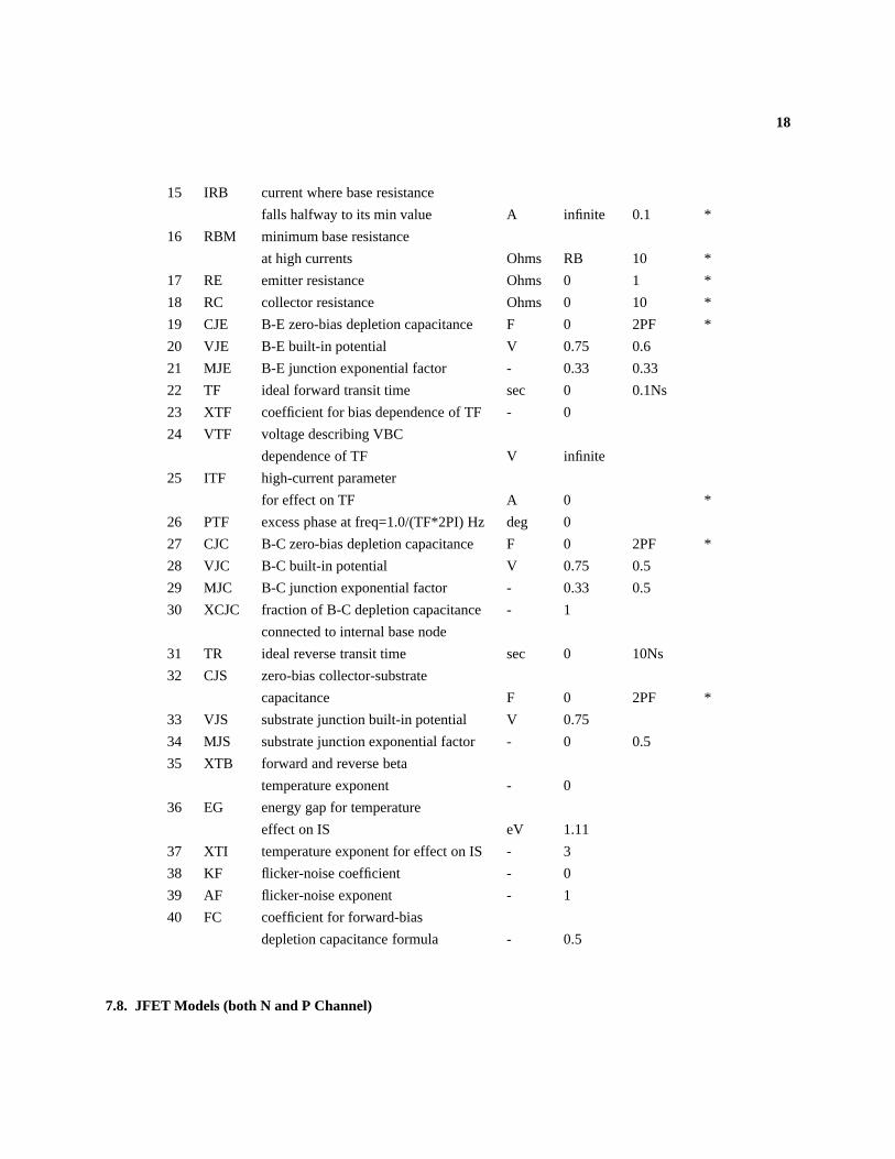
15 IRB current where base resistance
falls halfway to its min value A infinite 0.1 *
16 RBM minimum base resistance
at high currents Ohms RB 10 *
17 RE emitter resistance Ohms 0 1 *
18 RC collector resistance Ohms 0 10 *
19 CJE B-E zero-bias depletion capacitance F 0 2PF *
20 VJE B-E built-in potential V 0.75 0.6
21 MJE B-E junction exponential factor - 0.33 0.33
22 TF ideal forward transit time sec 0 0.1Ns
23 XTF coefficient for bias dependence of TF - 0
24 VTF voltage describing VBC
dependence of TF V infinite
25 ITF high-current parameter
for effect on TF A 0 *
26 PTF excess phase at freq=1.0/(TF*2PI) Hz deg 0
27 CJC B-C zero-bias depletion capacitance F 0 2PF *
28 VJC B-C built-in potential V 0.75 0.5
29 MJC B-C junction exponential factor - 0.33 0.5
30 XCJC fraction of B-C depletion capacitance - 1
connected to internal base node
31 TR ideal reverse transit time sec 0 10Ns
32 CJS zero-bias collector-substrate
capacitance F 0 2PF *
33 VJS substrate junction built-in potential V 0.75
34 MJS substrate junction exponential factor - 0 0.5
35 XTB forward and reverse beta
temperature exponent - 0
36 EG energy gap for temperature
effect on IS eV 1.11
37 XTI temperature exponent for effect on IS - 3
38 KF flicker-noise coefficient - 0
39 AF flicker-noise exponent - 1
40 FC coefficient for forward-bias
depletion capacitance formula - 0.5
7.8. JFET Models (both N and P Channel)

19
The JFET model is derived from the FET model of Shichman and Hodges. The dc characteristics are defined
by the parameters VTO and BETA, which determine the variation of drain current with gate voltage, LAMBDA,
which determines the output conductance, and IS, the saturation current of the two gate junctions. Two ohmic resis-
tances, RD and RS, are included. Charge storage is modeled by nonlinear depletion layer capacitances for both gate
junctions which vary as the -1/2 power of junction voltage and are defined by the parameters CGS, CGD, and PB.
name parameter units default example area
1 VTO threshold voltage V -2.0 -2.0
2 BETA transconductance parameter A/V**2 1.0E-4 1.0E-3 *
3 LAMBDA channel length modulation
parameter 1/V 0 1.0E-4
4 RD drain ohmic resistance Ohm 0 100 *
5 RS source ohmic resistance Ohm 0 100 *
6 CGS zero-bias G-S junction capacitance F 0 5PF *
7 CGD zero-bias G-D junction capacitance F 0 1PF *
8 PB gate junction potential V 1 0.6
9 IS gate junction saturation current A 1.0E-14 1.0E-14 *
10 KF flicker noise coefficient - 0
11 AF flicker noise exponent - 1
12 FC coefficient for forward-bias - 0.5
depletion capacitance formula
7.9. MOSFET Models (both N and P channel)
SPICE provides three MOSFET device models which differ in the formulation of the I-V characteristic. The
variable LEVEL specifies the model to be used:
LEVEL=1 -> Shichman-Hodges
LEVEL=2 -> MOS2 (as described in [1])
LEVEL=3 -> MOS3, a semi-empirical model(see [1])
The dc characteristics of the MOSFET are defined by the device parameters VTO, KP, LAMBDA, PHI and
GAMMA. These parameters are computed by SPICE if process parameters (NSUB, TOX, ...) are given, but user-
specified values always override. VTO is positive (negative) for enhancement mode and negative (positive) for
depletion mode N-channel (P-channel) devices. Charge storage is modeled by three constant capacitors, CGSO,
CGDO, and CGBO which represent overlap capacitances, by the nonlinear thin-oxide capacitance which is distri-
buted among the gate, source, drain, and bulk regions, and by the nonlinear depletion-layer capacitances for both
substrate junctions divided into bottom and periphery, which vary as the MJ and MJSW power of junction voltage
respectively, and are determined by the parameters CBD, CBS, CJ, CJSW, MJ, MJSW and PB. There are two

20
built-in models of the charge storage effects associated with the thin-oxide. The default is the piecewise linear
voltage-dependent capacitance model proposed by Meyer. The second choice is the charge-controlled capacitance
model of Ward and Dutton [1]. The XQC model parameter acts as a flag and a coefficient at the same time. As the
former it causes the program to use Meyer’s model whenever larger than 0.5 or not specified, and the charge-
controlled model when between 0 and 0.5. In the latter case its value defines the share of the channel charge associ-
ated with the drain terminal in the saturation region. The thin-oxide charge storage effects are treated slightly dif-
ferent for the LEVEL=1 model. These voltage-dependent capacitances are included only if TOX is specified in the
input description and they are represented using Meyer’s formulation.
There is some overlap among the parameters describing the junctions, e.g. the reverse current can be input
either as IS (in A) or as JS (in A/m**2). Whereas the first is an absolute value the second is multiplied by AD and
AS to give the reverse current of the drain and source junctions respectively. This methodology has been chosen
since there is no sense in relating always junction characteristics with AD and AS entered on the device card; the
areas can be defaulted. The same idea applies also to the zero-bias junction capacitances CBD and CBS (in F) on
one hand, and CJ (in F/m**2) on the other. The parasitic drain and source series resistance can be expressed as
either RD and RS (in ohms) or RSH (in ohms/sq.), the latter being multiplied by the number of squares NRD and
NRS input on the device card.
name parameter units default example
1 LEVEL model index - 1
2 VTO zero-bias threshold voltage V 0.0 1.0
3 KP transconductance parameter A/V**2 2.0E-5 3.1E-5
4 GAMMA bulk threshold parameter V**0.5 0.0 0.37
5 PHI surface potential V 0.6 0.65
6 LAMBDA channel-length modulation
(MOS1 and MOS2 only) 1/V 0.0 0.02
7 RD drain ohmic resistance Ohm 0.0 1.0
8 RS source ohmic resistance Ohm 0.0 1.0
9 CBD zero-bias B-D junction capacitance F 0.0 20FF
10 CBS zero-bias B-S junction capacitance F 0.0 20FF
11 IS bulk junction saturation current A 1.0E-14 1.0E-15
12 PB bulk junction potential V 0.8 0.87
13 CGSO gate-source overlap capacitance
per meter channel width F/m 0.0 4.0E-11
14 CGDO gate-drain overlap capacitance
per meter channel width F/m 0.0 4.0E-11
15 CGBO gate-bulk overlap capacitance
per meter channel length F/m 0.0 2.0E-10
16 RSH drain and source diffusion

21
sheet resisitance Ohm/sq. 0.0 10.0
17 CJ zero-bias bulk junction bottom cap.
per sq-meter of junction area F/m**2 0.0 2.0E-4
18 MJ bulk junction bottom grading coef. - 0.5 0.5
19 CJSW zero-bias bulk junction sidewall cap.
per meter of junction perimeter F/m 0.0 1.0E-9
20 MJSW bulk junction sidewall grading coef. - 0.33
21 JS bulk junction saturation current
per sq-meter of junction area A/m**2 1.0E-8
22 TOX oxide thickness meter 1.0E-7 1.0E-7
23 NSUB substrate doping 1/cm**3 0.0 4.0E15
24 NSS surface state density 1/cm**2 0.0 1.0E10
25 NFS fast surface state density 1/cm**2 0.0 1.0E10
26 TPG type of gate material: - 1.0
+1 opp. to substrate
-1 same as substrate
0 Al gate
27 XJ metallurgical junction depth meter 0.0 1U
28 LD lateral diffusion meter 0.0 0.8U
29 UO surface mobility cm**2/V-s 600 700
30 UCRIT critical field for mobility
degradation (MOS2 only) V/cm 1.0E4 1.0E4
31 UEXP critical field exponent in
mobility degradation (MOS2 only) - 0.0 0.1
32 UTRA transverse field coef (mobility)
(deleted for MOS2) - 0.0 0.3
33 VMAX maximum drift velocity of carriers m/s 0.0 5.0E4
34 NEFF total channel charge (fixed and
mobile) coefficient (MOS2 only) - 1.0 5.0
35 XQC thin-oxide capacitance model flag
and coefficient of channel charge
share attributed to drain (0-0.5) - 1.0 0.4
36 KF flicker noise coefficient - 0.0 1.0E-26
37 AF flicker noise exponent - 1.0 1.2
38 FC coefficient for forward-bias
depletion capacitance formula - 0.5
39 DELTA width effect on threshold voltage
(MOS2 and MOS3) - 0.0 1.0
40 THETA mobility modulation (MOS3 only) 1/V 0.0 0.1
41 ETA static feedback (MOS3 only) - 0.0 1.0
22
42 KAPPA saturation field factor (MOS3 only) - 0.2 0.5
[1] A. Vladimirescu and S. Liu, "The Simulation of MOS Integrated Circuits Using SPICE2", ERL Memo No. ERL
M80/7,Electronics Research Laboratory, University of California, Berkeley, Oct. 1980.
8. SUBCIRCUITS
A subcircuit that consists of SPICE elements can be defined and referenced in a fashion similar to device
models. The subcircuit is defined in the input deck by a grouping of element cards; the program then automatically
inserts the group of elements wherever the subcircuit is referenced. There is no limit on the size or complexity of
subcircuits, and subcircuits may contain other subcircuits. An example of subcircuit usage is given in Appendix A.
8.1. .SUBCKT Card
General form:
.SUBCKT subnam N1 <N2 N3 ...>
Examples:
.SUBCKT OPAMP 1 2 3 4
A circuit definition is begun with a .SUBCKT card. SUBNAM is the subcircuit name, and N1, N2, ... are the
external nodes, which cannot be zero. The group of element cards which immediately follow the .SUBCKT card
define the subcircuit. The last card in a subcircuit definition is the .ENDS card (see below). Control cards may not
appear within a subcircuit definition; however, subcircuit definitions may contain anything else, including other
subcircuit definitions, device models, and subcircuit calls (see below). Note that any device models or subcircuit
definitions included as part of a subcircuit definition are strictly local (i.e., such models and definitions are not
known outside the subcircuit definition). Also, any element nodes not included on the .SUBCKT card are strictly
local, with the exception of 0 (ground) which is always global.
8.2. .ENDS Card
General form:
.ENDS <SUBNAM>
Examples:
.ENDS OPAMP
This card must be the last one for any subcircuit definition. The subcircuit name, if included, indicates which
subcircuit definition is being terminated; if omitted, all subcircuits being defined are terminated. The name is
needed only when nested subcircuit definitions are being made.

23
8.3. Subcircuit Calls
General form:
XYYYYYYY N1 <N2 N3 ...> SUBNAM
Examples:
X1 2 4 17 3 1 MULTI
Subcircuits are used in SPICE by specifying pseudo-elements beginning with the letter X, followed by the cir-
cuit nodes to be used in expanding the subcircuit.

24
9. CONTROL CARDS
9.1. .TEMP Card
General form:
.TEMP T1 <T2 <T3 ...>>
Examples:
.TEMP -55.0 25.0 125.0
This card specifies the temperatures at which the circuit is to be simulated. T1, T2, ... Are the different tem-
peratures, in degrees C. Temperatures less than -223.0 deg C are ignored. Model data are specified at TNOM
degrees (see the .OPTIONS card for TNOM); if the .TEMP card is omitted, the simulation will also be performed at
a temperature equal to TNOM.
9.2. .WIDTH Card
General form:
.WIDTH IN=COLNUM OUT=COLNUM
Examples:
.WIDTH IN=72 OUT=133
COLNUM is the last column read from each line of input; the setting takes effect with the next line read.
The default value for COLNUM is 80. The out parameter specifies the output print width. Permissible values for
the output print width are 80 and 133.
9.3. .OPTIONS Card
General form:
.OPTIONS OPT1 OPT2 ... (or OPT=OPTVAL ...)
Examples:
.OPTIONS ACCT LIST NODE
This card allows the user to reset program control and user options for specific simulation purposes. Any
combination of the following options may be included, in any order. ’x’ (below) represents some positive number.
option effect
ACCT causes accounting and run time statistics to be printed
LIST causes the summary listing of the input data to be printed
25
NOMOD suppresses the printout of the model parameters.
NOPAGE suppresses page ejects
NODE causes the printing of the node table.
OPTS causes the option values to be printed.
GMIN=x resets the value of GMIN, the minimum conductance
allowed by the program. The default value is 1.0E-12.
RELTOL=x resets the relative error tolerance of the program. The
default value is 0.001 (0.1 percent).
ABSTOL=x resets the absolute current error tolerance of the
program. The default value is 1 picoamp.
VNTOL=x resets the absolute voltage error tolerance of the
program. The default value is 1 microvolt.
TRTOL=x resets the transient error tolerance. The default value
is 7.0. This parameter is an estimate of the factor by
which SPICE overestimates the actual truncation error.
CHGTOL=x resets the charge tolerance of the program. The default
value is 1.0E-14.
PIVTOL=x resets the absolute minimum value for a matrix entry
to be accepted as a pivot. The default value is 1.0E-13.
PIVREL=x resets the relative ratio between the largest column entry
and an acceptable pivot value. The default value is 1.0E-3.
In the numerical pivoting algorithm the allowed minimum
pivot value is determined by
EPSREL=AMAX1(PIVREL*MAXVAL,PIVTOL)
where MAXVAL is the maximum element in the column where
a pivot is sought (partial pivoting).
NUMDGT=x resets the number of significant digits printed for
output variable values. X must satisfy the relation
0 < x < 8. The default value is 4. Note: this option is
independent of the error tolerance used by SPICE (i.e., if
the values of options RELTOL, ABSTOL, etc., are not changed
then one may be printing numerical ’noise’ for NUMDGT > 4.
TNOM=x resets the nominal temperature. The default value is
27 deg C (300 deg K).
ITL1=x resets the dc iteration limit. The default is 100.
ITL2=x resets the dc transfer curve iteration limit. The
default is 50.
ITL3=x resets the lower transient analysis iteration limit.
the default value is 4.
ITL4=x resets the transient analysis timepoint iteration limit.

26
the default is 10.
ITL5=x resets the transient analysis total iteration limit.
the default is 5000. Set ITL5=0 to omit this test.
CPTIME=x the maximum cpu-time in seconds allowed for this job.
LIMTIM=x resets the amount of cpu time reserved by SPICE for
generating plots should a cpu time-limit cause job
termination. The default value is 2 (seconds).
LIMPTS=x resets the total number of points that can be printed
or plotted in a dc, ac, or transient analysis. The
default value is 201.
LVLCOD=x if x is 2 (two), then machine code for the matrix
solution will be generated. Otherwise, no machine code is
generated. The default value is 2. Applies only to CDC
computers.
LVLTIM=x if x is 1 (one), the iteration timestep control is used.
if x is 2 (two), the truncation-error timestep is used.
The default value is 2. If method=Gear and MAXORD>2 then
LVLTIM is set to 2 by SPICE.
METHOD=name sets the numerical integration method used by SPICE.
Possible names are Gear or trapezoidal. The default is
trapezoidal.
MAXORD=x sets the maximum order for the integration method if
Gear’s variable-order method is used. X must be between
2 and 6. The default value is 2.
DEFL=x resets the value for MOS channel length; the default
is 100.0 micrometer.
DEFW=x resets the value for MOS channel width; the default
is 100.0 micrometer.
DEFAD=x resets the value for MOS drain diffusion area; the
default is 0.0.
DEFAS=x resets the value for MOS source diffusion area; the
default is 0.0.
9.4. .OP Card
General form:
.OP

27
The inclusion of this card in an input deck will force SPICE to determine the dc operating point of the circuit
with inductors shorted and capacitors opened. Note: a dc analysis is automatically performed prior to a transient
analysis to determine the transient initial conditions, and prior to an ac small-signal analysis to determine the linear-
ized, small-signal models for nonlinear devices.
SPICE performs a dc operating point analysis if no other analyses are requested.
9.5. .DC Card
General form:
.DC SRCNAM VSTART VSTOP VINCR [SRC2 START2 STOP2 INCR2]
Examples:
.DC VIN 0.25 5.0 0.25
.DC VDS 0 10 .5 VGS 0 5 1
.DC VCE 0 10 .25 IB 0 10U 1U
This card defines the dc transfer curve source and sweep limits. SRCNAM is the name of an independent vol-
tage or current source. VSTART, VSTOP, and VINCR are the starting, final, and incrementing values respectively.
The first example will cause the value of the voltage source VIN to be swept from 0.25 Volts to 5.0 Volts in incre-
ments of 0.25 Volts. A second source (SRC2) may optionally be specified with associated sweep parameters. In
this case, the first source will be swept over its range for each value of the second source. This option can be useful
for obtaining semiconductor device output characteristics. See the second example data deck in that section of the
guide.
9.6. .NODESET Card
General form:
.NODESET V(NODNUM)=VAL V(NODNUM)=VAL ...
Examples:
.NODESET V(12)=4.5 V(4)=2.23
This card helps the program find the dc or initial transient solution by making a preliminary pass with the
specified nodes held to the given voltages. The restriction is then released and the iteration continues to the true
solution. The .NODESET card may be necessary for convergence on bistable or astable circuits. In general, this
card should not be necessary.
9.7. .IC Card
General form:
.IC V(NODNUM)=VAL V(NODNUM)=VAL ...
28
Examples:
.IC V(11)=5 V(4)=-5 V(2)=2.2
This card is for setting transient initial conditions. It has two different interpretations, depending on whether
the UIC parameter is specified on the .TRAN card. Also, one should not confuse this card with the .NODESET
card. The .NODESET card is only to help dc convergence, and does not affect final bias solution (except for multi-
stable circuits). The two interpretations of this card are as follows:
1. When the UIC parameter is specified on the .TRAN card, then the node voltages specified on the .IC card are
used to compute the capacitor, diode, BJT, JFET, and MOSFET initial conditions. This is equivalent to specifying
the IC=... parameter on each device card, but is much more convenient. The IC=... parameter can still be specified
and will take precedence over the .IC values. Since no dc bias (initial transient) solution is computed before the
transient analysis, one should take care to specify all dc source voltages on the .IC card if they are to be used to
compute device initial conditions.
2. When the UIC parameter is not specified on the .TRAN card, the dc bias (initial transient) solution will be com-
puted before the transient analysis. In this case, the node voltages specified on the .IC card will be forced to the
desired initial values during the bias solution. During transient analysis, the constraint on these node voltages is
removed.
9.8. .TF Card
General form:
.TF OUTVAR INSRC
Examples:
.TF V(5,3) VIN
.TF I(VLOAD) VIN
This card defines the small-signal output and input for the dc small- signal analysis. OUTVAR is the small-
signal output variable and INSRC is the small-signal input source. If this card is included, SPICE will compute the
dc small-signal value of the transfer function (output/input), input resistance, and output resistance. For the first
example, SPICE would compute the ratio of V(5,3) to VIN, the small-signal input resistance at VIN, and the small-
signal output resistance measured across nodes 5 and 3.
9.9. .SENS Card
General form:
.SENS OV1 <OV2 ... >
Examples:
.SENS V(9) V(4,3) V(17) I(VCC)

29
If a .SENS card is included in the input deck, SPICE will determine the dc small-signal sensitivities of each
specified output variable with respect to every circuit parameter. Note: for large circuits, large amounts of output
can be generated.
9.10. .AC Card
General form:
.AC DEC ND FSTART FSTOP
.AC OCT NO FSTART FSTOP
.AC LIN NP FSTART FSTOP
Examples:
.AC DEC 10 1 10K
.AC DEC 10 1K 100MEG
.AC LIN 100 1 100HZ
DEC stands for decade variation, and ND is the number of points per decade. OCT stands for octave varia-
tion, and NO is the number of points per octave. LIN stands for linear variation, and NP is the number of points.
FSTART is the starting frequency, and FSTOP is the final frequency. If this card is included in the deck, SPICE
will perform an ac analysis of the circuit over the specified frequency range. Note that in order for this analysis to
be meaningful, at least one independent source must have been specified with an ac value.
9.11. .DISTO Card
General form:
.DISTO RLOAD <INTER <SKW2 <REFPWR <SPW2>>>>
Examples:
.DISTO RL 2 0.95 1.0E-3 0.75
This card controls whether SPICE will compute the distortion characteristic of the circuit in a small-signal
mode as a part of the ac small-signal sinusoidal steady-state analysis. The analysis is performed assuming that one
or two signal frequencies are imposed at the input; let the two frequencies be f1 (the nominal analysis frequency)
and f2 (=SKW2*f1). The program then computes the following distortion measures:
HD2 - the magnitude of the frequency component 2*f1 assuming that f2
is not present.
HD3 - the magnitude of the frequency component 3*f1 assuming that f2
is not present.
SIM2 - the magnitude of the frequency component f1 + f2.
DIM2 - the magnitude of the frequency component f1 - f2.

30
DIM3 - the magnitude of the frequency component 2*f1 - f2.
RLOAD is the name of the output load resistor into which all distortion power products are to be computed.
INTER is the interval at which the summary printout of the contributions of all nonlinear devices to the total distor-
tion is to be printed. If omitted or set to zero, no summary printout will be made. REFPWR is the reference power
level used in computing the distortion products; if omitted, a value of 1 mW (that is, dbm) is used. SKW2 is the
ratio of f2 to f1. If omitted, a value of 0.9 is used (i.e., f2 = 0.9*f1). SPW2 is the amplitude of f2. If omitted, a
value of 1.0 is assumed.
The distortion measures HD2, HD3, SIM2, DIM2, and DIM3 may also be be printed and/or plotted (see the
description of the .PRINT and .PLOT cards).
9.12. .NOISE Card
General form:
.NOISE OUTV INSRC NUMS
Examples:
.NOISE V(5) VIN 10
This card controls the noise analysis of the circuit. The noise analysis is performed in conjunction with the ac
analysis (see .AC card). OUTV is an output voltage which defines the summing point. INSRC is the name of the
independent voltage or current source which is the noise input reference. NUMS is the summary interval. SPICE
will compute the equivalent output noise at the specified output as well as the equivalent input noise at the specified
input. In addition, the contributions of every noise generator in the circuit will be printed at every NUMS frequency
points (the summary interval). If NUMS is zero, no summary printout will be made.
The output noise and the equivalent input noise may also be printed and/or plotted (see the description of the
.PRINT and .PLOT cards).
9.13. .TRAN Card
General form:
.TRAN TSTEP TSTOP <TSTART <TMAX>> <UIC>
Examples:
.TRAN 1NS 100NS
.TRAN 1NS 1000NS 500NS
.TRAN 10NS 1US UIC
TSTEP is the printing or plotting increment for line-printer output. For use with the post-processor, TSTEP is
the suggested computing increment. TSTOP is the final time, and TSTART is the initial time. If TSTART is omit-
ted, it is assumed to be zero. The transient analysis always begins at time zero. In the interval <zero, TSTART>,
the circuit is analyzed (to reach a steady state), but no outputs are stored. In the interval <TSTART, TSTOP>, the

31
circuit is analyzed and outputs are stored. TMAX is the maximum stepsize that SPICE will use (for default, the pro-
gram chooses either TSTEP or (TSTOP-TSTART)/50.0, whichever is smaller. TMAX is useful when one wishes to
guarantee a computing interval which is smaller than the printer increment, TSTEP.
UIC (use initial conditions) is an optional keyword which indicates that the user does not want SPICE to solve
for the quiescent operating point before beginning the transient analysis. If this keyword is specified, SPICE uses
the values specified using IC=... on the various elements as the initial transient condition and proceeds with the
analysis. If the .IC card has been specified, then the node voltages on the .IC card are used to compute the intitial
conditions for the devices. Look at the description on the .IC card for its interpretation when UIC is not specified.
9.14. .FOUR Card
General form:
.FOUR FREQ OV1 <OV2 OV3 ...>
Examples:
.FOUR 100K V(5)
This card controls whether SPICE performs a Fourier analysis as a part of the transient analysis. FREQ is the
fundamental frequency, and OV1, ..., are the output variables for which the analysis is desired. The Fourier analysis
is performed over the interval <TSTOP-period, TSTOP>, where TSTOP is the final time specified for the transient
analysis, and period is one period of the fundamental frequency. The dc component and the first nine components
are determined. For maximum accuracy, TMAX (see the .TRAN card) should be set to period/100.0 (or less for
very high-Q circuits).
9.15. .PRINT Cards
General form:
.PRINT PRTYPE OV1 <OV2 ... OV8>
Examples:
.PRINT TRAN V(4) I(VIN)
.PRINT AC VM(4,2) VR(7) VP(8,3)
.PRINT DC V(2) I(VSRC) V(23,17)
.PRINT NOISE INOISE
.PRINT DISTO HD3 SIM2(DB)
This card defines the contents of a tabular listing of one to eight output variables. PRTYPE is the type of the
analysis (DC, AC, TRAN, NOISE, or DISTO) for which the specified outputs are desired. The form for voltage or
current output variables is as follows:
V(N1<,N2>)
specifies the voltage difference between nodes N1 and N2. If N2 (and the preceding comma) is

32
omitted, ground (0) is assumed. For the ac analysis, five additional outputs can be accessed by replac-
ing the letter V by:
VR - real part
VI - imaginary part
VM - magnitude
VP - phase
VDB - 20*log10(magnitude)
I(VXXXXXXX)
specifies the current flowing in the independent voltage source named VXXXXXXX. Positive current
flows from the positive node, through the source, to the negative node. For the ac analysis, the
corresponding replacements for the letter I may be made in the same way as described for voltage out-
puts.
Output variables for the noise and distortion analyses have a different general form from that of the other ana-
lyses, i.e.
OV<(X)>
where OV is any of ONOISE (output noise), INOISE (equivalent input noise), D2, HD3, SIM2, DIM2, or DIM3
(see description of distortion analysis), and X may be any of:
R - real part
I - imaginary part
M - magnitude (default if nothing specified)
P - phase
DB - 20*log10(magnitude)
thus, SIM2 (or SIM2(M)) describes the magnitude of the SIM2 distortion measure, while HD2(R) describes the real
part of the HD2 distortion measure.
There is no limit on the number of .PRINT cards for each type of analysis.
9.16. .PLOT Cards
General form:
.PLOT PLTYPE OV1 <(PLO1,PHI1)> <OV2 <(PLO2,PHI2)> ... OV8>
Examples:
.PLOT DC V(4) V(5) V(1)
.PLOT TRAN V(17,5) (2,5) I(VIN) V(17) (1,9)
.PLOT AC VM(5) VM(31,24) VDB(5) VP(5)
.PLOT DISTO HD2 HD3(R) SIM2

33
.PLOT TRAN V(5,3) V(4) (0,5) V(7) (0,10)
This card defines the contents of one plot of from one to eight output variables. PLTYPE is the type of
analysis (DC, AC, TRAN, NOISE, or DISTO) for which the specified outputs are desired. The syntax for the OVI
is identical to that for the .PRINT card, described above.
The optional plot limits (PLO,PHI) may be specified after any of the output variables. All output variables to
the left of a pair of plot limits (PLO,PHI) will be plotted using the same lower and upper plot bounds. If plot limits
are not specified, SPICE will automatically determine the minimum and maximum values of all output variables
being plotted and scale the plot to fit. More than one scale will be used if the output variable values warrant (i.e.,
mixing output variables with values which are orders-of-magnitude different still gives readable plots).
The overlap of two or more traces on any plot is indicated by the letter X.
When more than one output variable appears on the same plot, the first variable specified will be printed as
well as plotted. If a printout of all variables is desired, then a companion .PRINT card should be included.
There is no limit on the number of .PLOT cards specified for each type of analysis.

34
10. APPENDIX A: EXAMPLE DATA DECKS
10.1. Circuit 1
The following deck determines the dc operating point and small-signal transfer function of a simple differen-
tial pair. In addition, the ac small-signal response is computed over the frequency range 1Hz to 100MEGHz.
SIMPLE DIFFERENTIAL PAIRVCC 7 0 12VEE 8 0 -12VIN 1 0 AC 1RS1 1 2 1KRS2 6 0 1KQ1 3 2 4 MOD1Q2 5 6 4 MOD1RC1 7 3 10KRC2 7 5 10KRE 4 8 10K.MODEL MOD1 NPN BF=50 VAF=50 IS=1.E-12 RB=100 CJC=.5PF TF=.6NS.TF V(5) VIN.AC DEC 10 1 100MEG.PLOT AC VM(5) VP(5).PRINT AC VM(5) VP(5).END
10.2. Circuit 2
The following deck computes the output characteristics of a MOSFET device over the range 0-10V for VDS and 0-
5V for VGS.
MOS OUTPUT CHARACTERISTICS.OPTIONS NODE NOPAGEVDS 3 0VGS 2 0M1 1 2 0 0 MOD1 L=4U W=6U AD=10P AS=10P.MODEL MOD1 NMOS VTO=-2 NSUB=1.0E15 UO=550* VIDS MEASURES ID, WE COULD HAVE USED VDS, BUT ID WOULD BE NEGATIVEVIDS 3 1.DC VDS 0 10 .5 VGS 0 5 1.PRINT DC I(VIDS) V(2).PLOT DC I(VIDS).END

35
10.3. Circuit 3
The following deck determines the dc transfer curve and the transient pulse response of a simple RTL
inverter. The input is a pulse from 0 to 5 Volts with delay, rise, and fall times of 2ns and a pulse width of 30ns. The
transient interval is 0 to 100ns, with printing to be done every nanosecond.
SIMPLE RTL INVERTERVCC 4 0 5VIN 1 0 PULSE 0 5 2NS 2NS 2NS 30NSRB 1 2 10KQ1 3 2 0 Q1RC 3 4 1K.PLOT DC V(3).PLOT TRAN V(3) (0,5).PRINT TRAN V(3).MODEL Q1 NPN BF 20 RB 100 TF .1NS CJC 2PF.DC VIN 0 5 0.1.TRAN 1NS 100NS.END
10.4. Circuit 4
The following deck simulates a four-bit binary adder, using several subcircuits to describe various pieces of
the overall circuit.
ADDER - 4 BIT ALL-NAND-GATE BINARY ADDER
*** SUBCIRCUIT DEFINITIONS
.SUBCKT NAND 1 2 3 4* NODES: INPUT(2), OUTPUT, VCC
Q1 9 5 1 QMODD1CLAMP 0 1 DMODQ2 9 5 2 QMODD2CLAMP 0 2 DMODRB 4 5 4KR1 4 6 1.6KQ3 6 9 8 QMODR2 8 0 1KRC 4 7 130Q4 7 6 10 QMODDVBEDROP 10 3 DMODQ5 3 8 0 QMOD.ENDS NAND.SUBCKT ONEBIT 1 2 3 4 5 6
* NODES: INPUT(2), CARRY-IN, OUTPUT, CARRY-OUT, VCCX1 1 2 7 6 NAND

36
X2 1 7 8 6 NANDX3 2 7 9 6 NANDX4 8 9 10 6 NANDX5 3 10 11 6 NANDX6 3 11 12 6 NANDX7 10 11 13 6 NANDX8 12 13 4 6 NANDX9 11 7 5 6 NAND.ENDS ONEBIT.SUBCKT TWOBIT 1 2 3 4 5 6 7 8 9
* NODES: INPUT - BIT0(2) / BIT1(2), OUTPUT - BIT0 / BIT1,* CARRY-IN, CARRY-OUT, VCC
X1 1 2 7 5 10 9 ONEBITX2 3 4 10 6 8 9 ONEBIT.ENDS TWOBIT
.SUBCKT FOURBIT 1 2 3 4 5 6 7 8 9 10 11 12 13 14 15* NODES: INPUT - BIT0(2) / BIT1(2) / BIT2(2) / BIT3(2),* OUTPUT - BIT0 / BIT1 / BIT2 / BIT3, CARRY-IN, CARRY-OUT, VCC
X1 1 2 3 4 9 10 13 16 15 TWOBITX2 5 6 7 8 11 12 16 14 15 TWOBIT.ENDS FOURBIT
*** DEFINE NOMINAL CIRCUIT
.MODEL DMOD D
.MODEL QMOD NPN(BF=75 RB=100 CJE=1PF CJC=3PF)VCC 99 0 DC 5VVIN1A 1 0 PULSE(0 3 0 10NS 10NS 10NS 50NS)VIN1B 2 0 PULSE(0 3 0 10NS 10NS 20NS 100NS)VIN2A 3 0 PULSE(0 3 0 10NS 10NS 40NS 200NS)VIN2B 4 0 PULSE(0 3 0 10NS 10NS 80NS 400NS)VIN3A 5 0 PULSE(0 3 0 10NS 10NS 160NS 800NS)VIN3B 6 0 PULSE(0 3 0 10NS 10NS 320NS 1600NS)VIN4A 7 0 PULSE(0 3 0 10NS 10NS 640NS 3200NS)VIN4B 8 0 PULSE(0 3 0 10NS 10NS 1280NS 6400NS)X1 1 2 3 4 5 6 7 8 9 10 11 12 0 13 99 FOURBITRBIT0 9 0 1KRBIT1 10 0 1KRBIT2 11 0 1KRBIT3 12 0 1KRCOUT 13 0 1K.PLOT TRAN V(1) V(2) V(3) V(4) V(5) V(6) V(7) V(8).PLOT TRAN V(9) V(10) V(11) V(12) V(13).PRINT TRAN V(1) V(2) V(3) V(4) V(5) V(6) V(7) V(8).PRINT TRAN V(9) V(10) V(11) V(12) V(13)
*** (FOR THOSE WITH MONEY (AND MEMORY) TO BURN).TRAN 1NS 6400NS
.OPTIONS ACCT LIST NODE LIMPTS=6401
.END

37
10.5. Circuit 5
The following deck simulates a transmission-line inverter. Two transmission-line elements are required since
two propagation modes are excited. In the case of a coaxial line, the first line (T1) models the inner conductor with
respect to the shield, and the second line (T2) models the shield with respect to the outside world.
TRANSMISSION-LINE INVERTERV1 1 0 PULSE(0 1 0 0.1N)R1 1 2 50X1 2 0 0 4 TLINER2 4 0 50.SUBCKT TLINE 1 2 3 4T1 1 2 3 4 Z0=50 TD=1.5NST2 2 0 4 0 Z0=100 TD=1NS.ENDS TLINE.TRAN 0.1NS 20NS.PLOT TRAN V(2) V(4).END
38
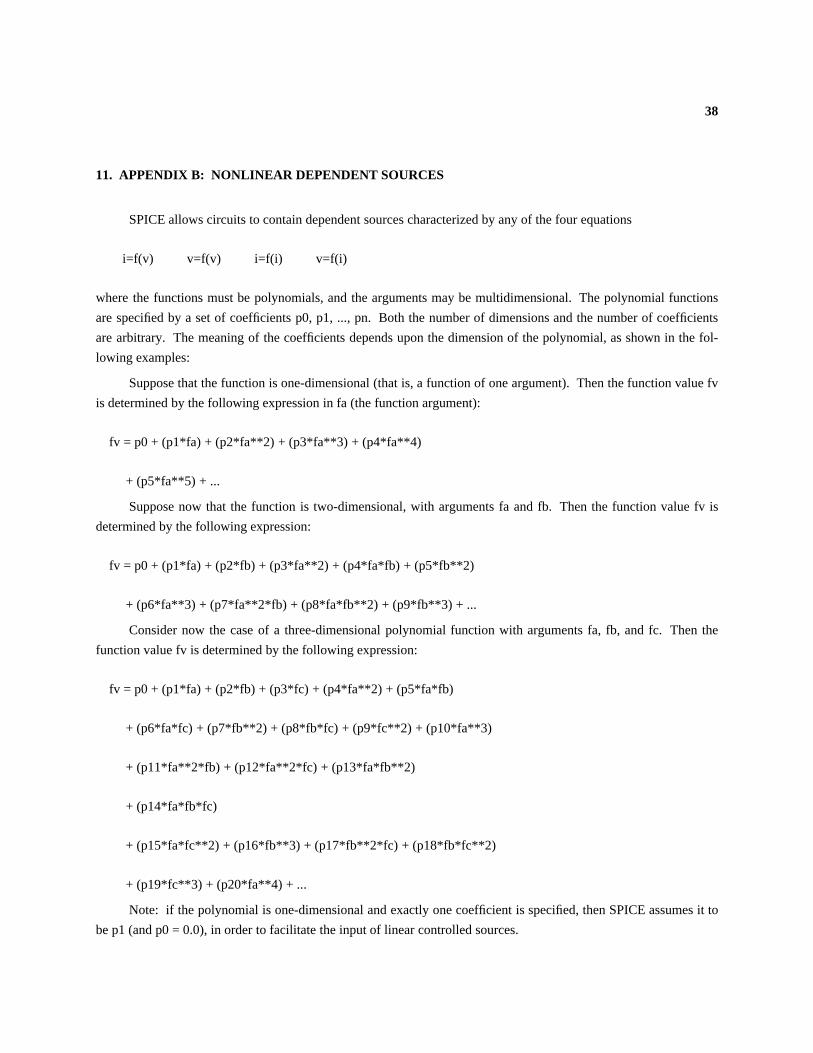
11. APPENDIX B: NONLINEAR DEPENDENT SOURCES
SPICE allows circuits to contain dependent sources characterized by any of the four equations
i=f(v) v=f(v) i=f(i) v=f(i)
where the functions must be polynomials, and the arguments may be multidimensional. The polynomial functions
are specified by a set of coefficients p0, p1, ..., pn. Both the number of dimensions and the number of coefficients
are arbitrary. The meaning of the coefficients depends upon the dimension of the polynomial, as shown in the fol-
lowing examples:
Suppose that the function is one-dimensional (that is, a function of one argument). Then the function value fv
is determined by the following expression in fa (the function argument):
fv = p0 + (p1*fa) + (p2*fa**2) + (p3*fa**3) + (p4*fa**4)
+ (p5*fa**5) + ...
Suppose now that the function is two-dimensional, with arguments fa and fb. Then the function value fv is
determined by the following expression:
fv = p0 + (p1*fa) + (p2*fb) + (p3*fa**2) + (p4*fa*fb) + (p5*fb**2)
+ (p6*fa**3) + (p7*fa**2*fb) + (p8*fa*fb**2) + (p9*fb**3) + ...
Consider now the case of a three-dimensional polynomial function with arguments fa, fb, and fc. Then the
function value fv is determined by the following expression:
fv = p0 + (p1*fa) + (p2*fb) + (p3*fc) + (p4*fa**2) + (p5*fa*fb)
+ (p6*fa*fc) + (p7*fb**2) + (p8*fb*fc) + (p9*fc**2) + (p10*fa**3)
+ (p11*fa**2*fb) + (p12*fa**2*fc) + (p13*fa*fb**2)
+ (p14*fa*fb*fc)
+ (p15*fa*fc**2) + (p16*fb**3) + (p17*fb**2*fc) + (p18*fb*fc**2)
+ (p19*fc**3) + (p20*fa**4) + ...
Note: if the polynomial is one-dimensional and exactly one coefficient is specified, then SPICE assumes it to
be p1 (and p0 = 0.0), in order to facilitate the input of linear controlled sources.

39
For all four of the dependent sources described below, the initial condition parameter is described as optional.
If not specified, SPICE assumes 0 the initial condition for dependent sources is an initial ’guess’ for the value of the
controlling variable. The program uses this initial condition to obtain the dc operating point of the circuit. After
convergence has been obtained, the program continues iterating to obtain the exact value for the controlling vari-
able. Hence, to reduce the computational effort for the dc operating point (or if the polynomial specifies a strong
nonlinearity), a value fairly close to the actual controlling variable should be specified for the initial condition.
11.1. Voltage-Controlled Current Sources
General form:
GXXXXXXX N+ N- <POLY(ND)> NC1+ NC1- ... P0 <P1 ...> <IC=...>
Examples:
G1 1 0 5 3 0 0.1MGR 17 3 17 3 0 1M 1.5M IC=2VGMLT 23 17 POLY(2) 3 5 1 2 0 1M 17M 3.5U IC=2.5, 1.3
N+ and N- are the positive and negative nodes, respectively. Current flow is from the positive node, through
the source, to the negative node. POLY(ND) only has to be specified if the source is multi-dimensional (one-
dimensional is the default). If specified, ND is the number of dimensions, which must be positive. NC1+, NC1-, ...
Are the positive and negative controlling nodes, respectively. One pair of nodes must be specified for each dimen-
sion. P0, P1, P2, ..., Pn are the polynomial coefficients. The (optional) initial condition is the initial guess at the
value(s) of the controlling voltage(s). If not specified, 0.0 is assumed. The polynomial specifies the source current
as a function of the controlling voltage(s). The second example above describes a current source with value
I = 1E-3*V(17,3) + 1.5E-3*V(17,3)**2
note that since the source nodes are the same as the controlling nodes, this source actually models a nonlinear resis-
tor.

40
11.2. Voltage-Controlled Voltage Sources
General form:
EXXXXXXX N+ N- <POLY(ND)> NC1+ NC1- ... P0 <P1 ...> <IC=...>
Examples:
E1 3 4 21 17 10.5 2.1 1.75EX 17 0 POLY(3) 13 0 15 0 17 0 0 1 1 1 IC=1.5,2.0,17.35
N+ and N- are the positive and negative nodes, respectively. POLY(ND) only has to be specified if the
source is multi-dimensional (one-dimensional is the default). If specified, ND is the number of dimensions, which
must be positive. NC1+, NC1-, ... are the positive and negative controlling nodes, respectively. One pair of nodes
must be specified for each dimension. P0, P1, P2, ..., Pn are the polynomial coefficients. The (optional) initial con-
dition is the initial guess at the value(s) of the controlling voltage(s). If not specified, 0.0 is assumed. The polyno-
mial specifies the source voltage as a function of the controlling voltage(s). The second example above describes a
voltage source with value
V = V(13,0) + V(15,0) + V(17,0)
(in other words, an ideal voltage summer).
11.3. Current-Controlled Current Sources
General form:
FXXXXXXX N+ N- <POLY(ND)> VN1 <VN2 ...> P0 <P1 ...> <IC=...>
Examples:
F1 12 10 VCC 1MA 1.3MFXFER 13 20 VSENS 0 1
N+ and N- are the positive and negative nodes, respectively. Current flow is from the positive node, through
the source, to the negative node. POLY(ND) only has to be specified if the source is multi-dimensional (one-
dimensional is the default). If specified, ND is the number of dimensions, which must be positive. VN1, VN2, ...
are the names of voltage sources through which the controlling current flows; one name must be specified for each
dimension. The direction of positive controlling current flow is from the positive node, through the source, to the
negative node of each voltage source. P0, P1, P2, ..., Pn are the polynomial coefficients. The (optional) initial con-
dition is the initial guess at the value(s) of the controlling current(s) (in Amps). If not specified, 0.0 is assumed.
The polynomial specifies the source current as a function of the controlling current(s). The first example above
describes a current source with value
I = 1E-3 + 1.3E-3*I(VCC)
41
11.4. Current-Controlled Voltage Sources
General form:
HXXXXXXX N+ N- <POLY(ND)> VN1 <VN2 ...> P0 <P1 ...> <IC=...>
Examples:
HXY 13 20 POLY(2) VIN1 VIN2 0 0 0 0 1 IC=0.5 1.3HR 4 17 VX 0 0 1
N+ and N- are the positive and negative nodes, respectively. POLY(ND) only has to be specified if the
source is multi-dimensional (one-dimensional is the default). If specified, ND is the number of dimensions, which
must be positive. VN1, VN2, ... are the names of voltage sources through which the controlling current flows; one
name must be specified for each dimension. The direction of positive controlling current flow is from the positive
node, through the source, to the negative node of each voltage source. P0, P1, P2, ..., Pn are the polynomial
coefficients. The (optional) initial condition is the initial guess at the value(s) of the controlling current(s) (in
Amps). If not specified, 0.0 is assumed. The polynomial specifies the source voltage as a function of the controlling
current(s). The first example above describes a voltage source with value
V = I(VIN1)*I(VIN2)
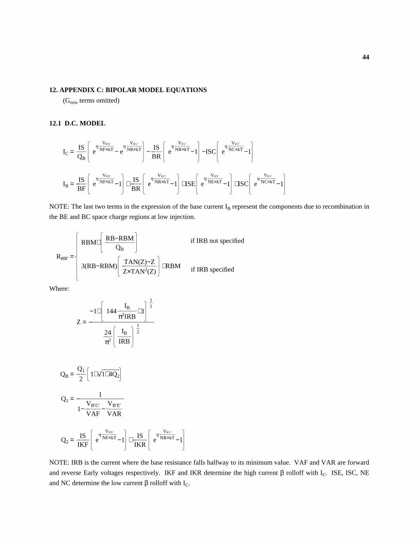
44
12. APPENDIX C: BIPOLAR MODEL EQUATIONS
(Gmin terms omitted)
12.1 D.C. MODEL
IC =QB
IShhhIJL
eq
NF×kTVB′E′hhhhhhh
− eq
NR×kTVB′C′hhhhhhh M
JO−
BRIShhhh
IJL
eq
NR×kTVB′C′hhhhhhh
−1MJO−ISC
IJL
eq
NC×kTVB′C′hhhhhhh
−1MJO
IB =BFIShhhh
IJL
eq
NF×kTVB′E′hhhhhhh
−1MJO+
BRIShhhh
IJL
eq
NR×kTVB′C′hhhhhhh
−1MJO+ISE
IJL
eq
NE×kTVB′E′hhhhhhh
−1MJO+ISC
IJL
eq
NC×kTVB′C′hhhhhhh
−1MJO
NOTE: The last two terms in the expression of the base current IB represent the components due to recombination in
the BE and BC space charge regions at low injection.
RBB′ =
IJJKJJL
3(RB−RBM)IJL Z×TAN2(Z)
TAN(Z)−ZhhhhhhhhhhhMJO+RBM
RBM+IJL QB
RB−RBMhhhhhhhhhMJO
if IRB specified
if IRB not specified
Where:
Z =
π2
24hhhIJL IRB
IBhhhhMJO
21hh
−1+IJL
144π2IRB
IBhhhhhh+1MJO
21hh
hhhhhhhhhhhhhhhhhhhh
QB =2
Q1hhh IL1+√ddddd1+4Q2
MO
Q1 =1−
VAF
VB′C′hhhhh−VAR
VB′E′hhhhh
1hhhhhhhhhhhhhhh
Q2 =IKFIShhhh
IJL
eq
NF×kTVB′E′hhhhhhh
−1MJO+
IKRIShhhhh
IJL
eq
NR×kTVB′C′hhhhhhh
−1MJO
NOTE: IRB is the current where the base resistance falls halfway to its minimum value. VAF and VAR are forward
and reverse Early voltages respectively. IKF and IKR determine the high current β rolloff with IC. ISE, ISC, NE
and NC determine the low current β rolloff with IC.

45
12.2 A.C. MODEL
CBE =∂VB′E′
∂hhhhhhIJJL
TFF×QB
IShhhIJL
eq
NF×kTVB′E′hhhhhhh
−1MJO
MJJO
+CJEIJL
1−VJE
VB′E′hhhhhMJO
−MJ
Where:
TFF = TF
IJJL
1+XTFIJL
e 1.44VTFVB′C′hhhhhhhh M
JO
IJL IF+ITF
IFhhhhhhhMJO
2 MJJO
IF = ISIJL
eq
NF×kTVB′E′hhhhhhh
−1MJO
CB1 = CBC(1−XCJC)
CB2 = CBC × XCJC
CBC = TRIJL NR×kT
qIShhhhhhh eq
kTVB′C′hhhhh M
JO+CJC
IJL
1−VJC
VB′C′hhhhhMJO
−MJC
CSS = CJSIJL1−
VJS
VC′S′hhhhhMJO
−MJS
NOTE: all junction capacitances of the form C0
IJL1−
φVhhh
MJO
−M
revert to the form
(1−FC)M
C0hhhhhhhhRJQ
1+φ(1−FC)
Mhhhhhhhh(V−FC×φ)HJP
when V > FC×φ ( For CSS assumes FC = 0 )
12.3 EXCESS PHASE
This is a delay (linear phase) in the gm generator in AC analysis. It is also used in transient analysis using a Bessel
polynomial approximation. Excess phase, PTF, is specified as the number of extra degrees of phase at the frequency
f =2πTF
1hhhhhh Hertz

46
12.4 TEMPERATURE EFFECTS
All junctions have dependences identical to the diode model but all N factors are considered equal 1.
βF and βR go asIJL TNOM
ThhhhhhhMJO
XTB
when NF=1.
This is done through appropriate changes in βF , βR and ISE, ISC according to the following equations respec-
tively:
β′F or R = BF (orBR)IJL TNOM
ThhhhhhhMJO
XTB
ISE′ ( or ISC′) =IJL TNOM
ThhhhhhhMJO
XTB
ISE ( or ISC)IJL TNOM
ThhhhhhhMJO
XTI IJL
eNk
qEGhhhhh×IJL T×TNOM
T−TNOMhhhhhhhhhMJOMJOhhhhhhhhhhhhhhhhhhhhhhhhhhhhhhhhhhhhhhh
12.5 NOISE MODEL
IRE
hhh2 =
RE4kThhhh∆f
IRC
hhh2 =
RC4kThhhh∆f
IRBB′
hhh2 =
RBB′
4kThhhhh∆fMJJJNJJJO
Thermal noise
IBN
hhh2 = 2qIB∆f+
f
KF×IBAF
hhhhhhh∆f
Note: The first term is shot noise and the second term is flicker noise.
ICN
hhh2 = 2qIC∆f
Note: This is shot noise.

47
12. APPENDIX D: ALTER STATEMENT AND THE SOURCE-STEPPING METHOD
The ALTER statement allows SPICE to run with altered circuit parameters.
General form:
.ALTERELEMENT CARDS (DEVICE CARDS, MODEL CARDS).ALTER (or .END CARD)
Examples:
R1 1 0 5KVCC 3 0 10M1 3 2 0 MOD1 L=5U W=2U.MODEL MOD1 NMOS(VTO=1.0 KP=2.0E-5 PHI=0.6 NSUB=2.0E15 TOX=0.1U).ALTERR1 1 0 3.5KVCC 3 0 12M1 3 2 0 MOD1 L=10U W=2U.MODEL MOD1 NMOS(VTO=1.2 KP=2.0E-5 PHI=0.6 NSUB=5.0E15 TOX=1.5U).ALTERM1 3 2 0 MOD1 L=10U W=4U.END
This card introduces the element(s), device(s) and model(s) whose parameters are changed during the execu-
tion of the input deck. The analyses specified in the deck will start over again with the changed parameters. The
.ALTER card with the cards defining the new parameters should be placed just before the .END card. The syntax
for the element (device, model) cards is identical to that of the cards with the original parameters.
There is no limit on the number of .ALTER cards and the circuit will be re-analyzed as many times as the
number of .ALTER cards. Subsequent ALTER operations employ parameters of the previous change. No topologi-
cal change of the circuit is allowed.
The source-stepping method can enhance DC convergence. But it is slower than direct use of the Newton-
Raphson method. Therefore it is best used as an alternative to achieve convergence of DC operating point when the
circuit fails to converge by using the Newton-Raphson method. The source-stepping method is used by SPICE
when the variable ITL6 in the .OPTIONS card is set to the iteration limit at each step of the source(s).
For example,
.OPTIONS ITL6=30
will cause SPICE to use source-stepping method with iteration limit 30 at each step. By default, ITL6 is 0 which
means to use the Newton-Raphson method directly.
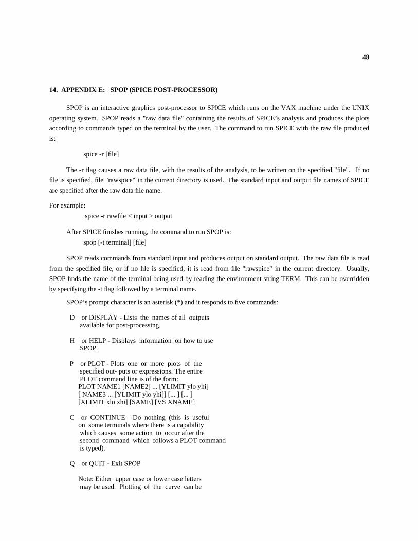
48
14. APPENDIX E: SPOP (SPICE POST-PROCESSOR)
SPOP is an interactive graphics post-processor to SPICE which runs on the VAX machine under the UNIX
operating system. SPOP reads a "raw data file" containing the results of SPICE’s analysis and produces the plots
according to commands typed on the terminal by the user. The command to run SPICE with the raw file produced
is:
spice -r [file]
The -r flag causes a raw data file, with the results of the analysis, to be written on the specified "file". If no
file is specified, file "rawspice" in the current directory is used. The standard input and output file names of SPICE
are specified after the raw data file name.
For example:
spice -r rawfile < input > output
After SPICE finishes running, the command to run SPOP is:
spop [-t terminal] [file]
SPOP reads commands from standard input and produces output on standard output. The raw data file is read
from the specified file, or if no file is specified, it is read from file "rawspice" in the current directory. Usually,
SPOP finds the name of the terminal being used by reading the environment string TERM. This can be overridden
by specifying the -t flag followed by a terminal name.
SPOP’s prompt character is an asterisk (*) and it responds to five commands:
D or DISPLAY - Lists the names of all outputsavailable for post-processing.
H or HELP - Displays information on how to useSPOP.
P or PLOT - Plots one or more plots of thespecified out- puts or expressions. The entirePLOT command line is of the form:PLOT NAME1 [NAME2] ... [YLIMIT ylo yhi][ NAME3 ... [YLIMIT ylo yhi]] [... ] [... ][XLIMIT xlo xhi] [SAME] [VS XNAME]
C or CONTINUE - Do nothing (this is usefulon some terminals where there is a capabilitywhich causes some action to occur after thesecond command which follows a PLOT commandis typed).
Q or QUIT - Exit SPOP
Note: Either upper case or lower case lettersmay be used. Plotting of the curve can be
49
interrupted by hitting BREAK key on theterminal.
The parameters of the PLOT command are defined below:
NAME1, NAME2, NAME3 and XNAME can be simple namesof outputs as given by the DISPLAY command, orsimple or complex expressions as described below.
The backslash is the plot delimiter and is usedfor defining more than one plot per display.
YLIMIT (or YLI) sets the Y-axis limits to ("ylo","yhi"). If not given, limits are chosen to bestfit the data.
XLIMIT (or XLI) sets the X-axis limits to ("xlo","xhi"). If not given, limits are chosen to bestfit the data.
SAME is used to add new data to an existing plot,i.e. plot a new curve on the screen using theprevious grid and without erasing the existingplots.
VS specifies the variable or function to be usedfor the X axis. If VS is not specified, thedefault "sweep variable" is used.
Note: The VS parameter can only be specified onceper PLOT command.
Since complex values cannot be plotted, SPOP allows components of complex values to be computed. To
specify the component of a single variable, one of the following strings should be appended to the variable name:
M - MagnitudeP - Phase (degrees)DB - 20*LOG(Magnitude)R - Real partI - Imaginary part
For example, to plot the magnitude of I(V1), use PLOT IM(V1).
To get the components of expressions, the following functions should be used:
MAG(expression) magnitudePH(expression) phase (in degrees)J(expression) convert real value to imaginary
valueREAL(expression) real partIMAG(expression) imaginary part

50
The "NAMES" in the PLOT command may be algebraic expressions. The legal operators in expressions are:
+ addition- subtraction* multiplication/ divisionˆ exponentiation
For example, to get the real component of V(1)+V(2), use REAL(V(1)+V(2)).
There are also nine built-in functions which may be used in expressions:
LOG() logarithm base 10LN() natural logarithmEXP() power of eABS() absolute valueSQRT() square rootSIN() sineCOS() cosineTAN() tangentATAN() arctangent
For example, to get the absolute value of V(3)*V(4), use ABS(V(3)*V(4)).
The following are the names of terminals which have the capability to run SPOP at the present time:
HP2648, AED512, VT125


![arXiv:1505.01549v2 [astro-ph.SR] 26 Aug 2015 · ried by Leach & Petrosian (1981) who treated the transport and radiation by electrons using the Fokker-Planck transport](https://static.fdocuments.us/doc/165x107/5aca895b7f8b9a40728e4bb2/arxiv150501549v2-astro-phsr-26-aug-2015-by-leach-petrosian-1981-who-treated.jpg)