
Distributed Process Management: Distributed Global States and Distributed Mutual Exclusion

1. Introduction
We propose to develop a distributed of small sensors that can monitor the environment, communicate with eachother, perform distributed computations, and reach joint decisions by fusing the data the individual sensors acquire. Each node of the network will be composed of several sensors, a microprocessor and a transceiver. We expect there to be anywhere from ten to hundreds and perhaps thousands of nodes in the network. The connectivity of the network will depend on the transmitting power and the distance between nodes. We expect nodes be at least be able to transmit to their nearest neighbors. Figure 1 illustrates the ad-hoc sensor networks.
To design and fabricate the network, we will use a combination of new hardware and software algorithims. The unique aspects of the proposed network will include:
Use of both narrow band operation for communication and ultra-wide band for localization.
Integration of MEMS chemical and vibrational sensors.
Unique signal processing algorithms to decipher sensed data.
Development of our own application specific integrated circuits (ICs), as well as incorporation of existing ICs.
Application of 3-dimensional fabrication technology where integrated circuits can be stacked vertically.
Application of unique antenna designs and high-K dielectrics that allow for use of unusually small geometries.
Extremely high value micron size 3D interdigitated capacitors to facilitate energy storage in very small volumes.
Unique algorithms for localization.
In order to achieve processing, fusion and localization across the network, we plan to utilize energy-efficient short-range RF communication, sensing and processing at each node and develop ad-hoc networking algorithms for reliable communication and fusion. The network will exploit multiplexing of transmissions in time and frequency, by combining time-division multiple access (TDMA) with frequency-division multiple access (FDMA). We plan to have the network self-assemble whereby the multiple access slots are reused across the network with large enough reuse distances to avoid interference. As a result, each particle will communicate “within its cell” with a small number of nodes, at a small number of operating frequencies, and a small number of time allocations. Information will be sensed and will then be fused with that of other particles to make network-wide decisions. The information will be communicated digitally using frequency shift
Figure 1: Illustration of Ad-Hoc Sensor Network
keying (FSK) modulation. Location determination will be achieved through a combination of algorithms, which will rely on both narrow and ultra-wide band communication.
To achieve our goals we plan to work in three phases. During each phase more aggressive scaling will be achieved, and more complex networks will be developed.
* Phase 1:Smart Stones (several centermeter scale): In the first phase of our program, we plan to develop an ad-hoc network of between ten and twenty nodes. These “Smart Stone” nodes will be several centimeters in dimension. Each smart stone will contain a narrow band transceiver, a microprocessor, and one or more of the following sensors: vibrational, acoustical, temperature and optical. An ultra-wideband transceiver may also be included to help perform location determination. The system will be integrated into a multi-level device, fabricated on printed circuit (PC) boards. The smart stones will mainly commercially off the shelf (COTS) integrated circuits. Of course, a standard GPS receiver can readily be included into the smart stone unit for outdoor location with meter level accuracy. The network will assemble itself and establish communications using a TDMA protocol.
* Phase 2: Smart Pebbles (sub-centimeter scale): In Phase 2, we will concentrate on reducing the size of our sensor nodes to sub-centimeter dimensions. To achieve we will use both, COTS parts, as well as IC’s that we design and fabricate ourselves. As we have done in previously, the fabrication process will be accomplished using the MOSIS facility, and the post processing will be performed at local laboratories. (The MOSIS facility allows for the fabrication of chips, in lots consisting of 40 die, that are well within the Phase 2 budget of this project.) To reduce the antenna geometry required, we will increase the operating frequency of our circuits, as well as use high-K dielectric antenna substrates. We also plan to increase the number of nodes from between the 10 and 20 developed in Phase 1, to approximately 100 in Phase 2. In this phase, 3D stacking of chips will be performed to greatly reduce the footprint.
* Phase 3: Smart Dust (millimeter scale): In Phase 3 we will further concentrate on reducing the scale of our nodes into the millimeter range. This will require moving to 3D fabrication of nodes using our own chips, and where possible, existing IC’s. In Phase 3 we plan to increase the number of nodes in the network, design and prototype millimeter sized nodes, which we will call smart dust. Finally, we plan to organize with manufacturers to produce Smart Pebbles and Smart Dust in large volumes. Once this is accomplished, we will apply our networking and signal processing algorithms over networks that may contain hundreds, or even thousands of smart particles.
2. Phase 1: Project Description
In Phase 1 of the program we will develop an ad-hoc, sefl-assembled network of approximately twenty smart stones. The overall plans were described in the bullet item in Section 1. Here, we describe more details of the Phase 1 hardware and network algorithms.
2.1 Smart Stone Hardware

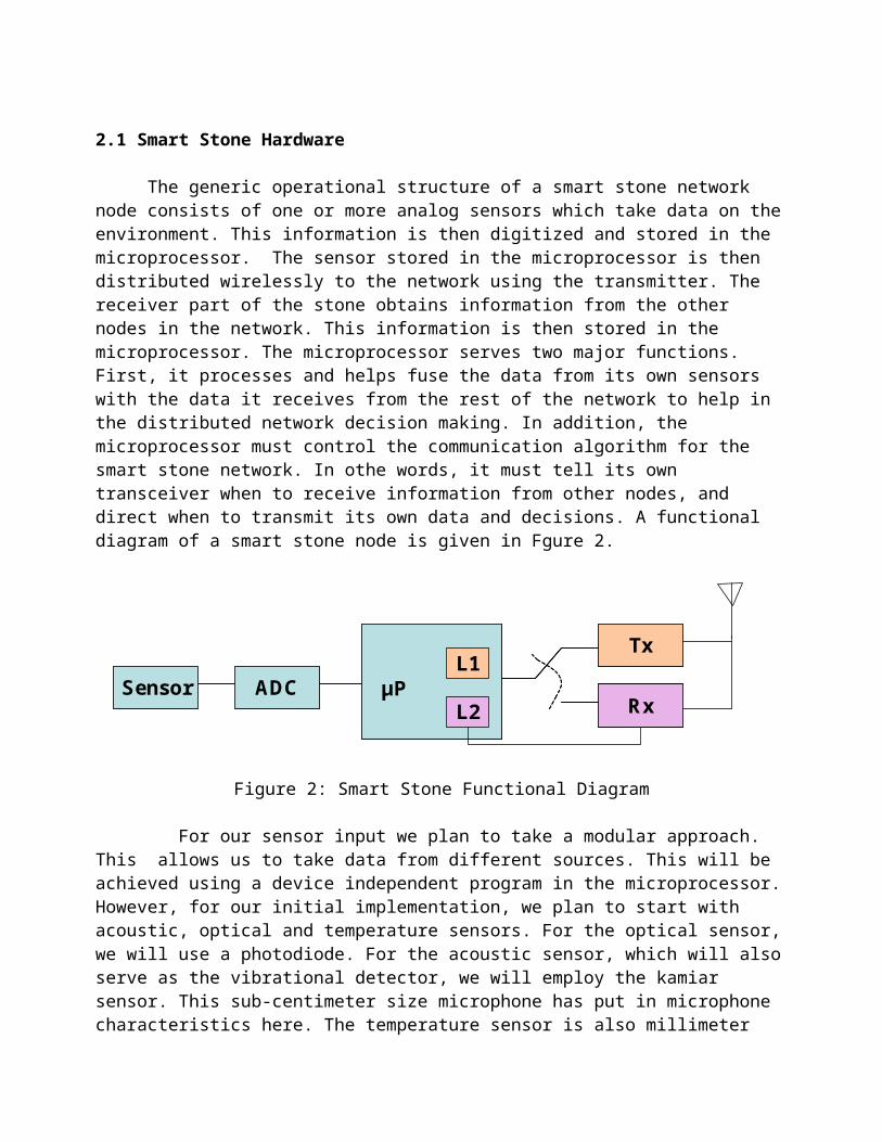
The generic operational structure of a smart stone network node consists of one or more analog sensors which take data on the environment. This information is then digitized and stored in the microprocessor. The sensor stored in the microprocessor is then distributed wirelessly to the network using the transmitter. The receiver part of the stone obtains information from the other nodes in the network. This information is then stored in the microprocessor. The microprocessor serves two major functions. First, it processes and helps fuse the data from its own sensors with the data it receives from the rest of the network to help in the distributed network decision making. In addition, the microprocessor must control the communication algorithm for the smart stone network. In othe words, it must tell its own transceiver when to receive information from other nodes, and direct when to transmit its own data and decisions. A functional diagram of a smart stone node is given in Fgure 2.
L1
L2μP
L1
L2μPSensor ADCSensor ADC
Tx
Rx
TxTx
RxRx
Figure 2: Smart Stone Functional Diagram For our sensor input we plan to take a modular approach. This allows us to take data from different sources. This will be achieved using a device independent program in the microprocessor. However, for our initial implementation, we plan to start with acoustic, optical and temperature sensors. For the optical sensor, we will use a photodiode. For the acoustic sensor, which will also serve as the vibrational detector, we will employ the kamiar sensor. This sub-centimeter size microphone has put in microphone characteristics here. The temperature sensor is also millimeter sized, and provides a put temperature sensor characteristics here. In our background work we have already investigated the characteristics of these sensors. Where necessary, we will provide the analog to digital (ADC) interface required between the analog sensor and the microcprocessor. For our initial prototypes, this interface will be provided with the XXX ADC converter. Figure 3 shows the prototyped sensor systems mounted on small PC boards we designed and fabricated in our background investigation.
Put Figure 3 here: Microphone and Temp sensor boards
In our background work preparing for Phase 1 we have been using the Microchip PIC16F628 controller. This micro-controller is robust and very inexpensive. We have aquired considerable experience developing assembly language communication protocols using the PIC, and have developed a considerable library of codes to implement data acquisition and digital communication.
Overall, its versitility, power management, price and assortment of op-codes make is suitable for use in implementing the smart stone network. During our Phase 1, in addition continuing our work with Microchip controller, we also plan to investigate the Chipcon 1010 and Texas Instrument XXX microcontrollers. The advantage of the Chipcon system, is that it contains both a microprocessor and transceiver in the same compact package compact package. The TI XXX has advantages of extremely low power consumption.
In our background work using COTS transmitters and receivers, we have accomplished much or our wireless transmission using the Linx receiver/transmitters pairs. The Linx916ES transmitter and receiver pair operate using frequency modulation (FM) about a narrow band carrier of 916MHz. Applying a serial stream of bits will allow for Frequency Shift Keying (FSK) transmission of bits for digital communication over the network. The Linx transmitter and receiver can operate at serial baud rates of approximately 200,000. While this does not represent an extremely high rate of transfer, it will be sufficient for performing distributed processing on the data obtained from the acoustic, temperature and optical sensors which vary on a time scale of approximately 100milliseconds.
In addition to continuing our work with the Linx system for transceiver development, we also plan to develop a prototype using the combined Chipcon 1010 transceiver/microntroller IC. A comparison will between the Linx-based and Chipcon-based systems will then be made to determine which is better suited for the distributed sensor network application. Figure 4 shows a prototype we developed in our background work which uses the Linx transmitter system in coordination with the PIC microcontroller.
2.2 Communication Protocols for the Smart Stone Network (Gil, please try to make this sound more intelligent)
We plan to use a combination of TDMA and FDMA for networking the individual nodes. This will allow us to use both frequency and time domains for efficient transmission of data. In Phase 1 we will implement our system using TDMA, and design the FDMA/TDMA algorithm. In Phase 2 we plan to add the FDMA hardware and software components to the network. In developing the communication protocols we must
Source and Channel CodingTo communicate effectively we will establish channels between nodes. We will develop algorithms for source and channel coding that are optimal for the transmission of data extracted from analog sensors. Source coding algorithms will accomplish efficient analog to digital conversion. In most cases this will be performed by the microprocessor. We will then determine methods to most
Figure 4: Transceiver Prototype Developed as Background to Phase 1

efficiently transmit information using the minimum number of bytes. For example, specific type of data and information that is sent frequently will be represented by very simple bit patterns that are error tolerant, while data-types that are seldom transferred will require more energy to send. Data compression algorithms directed at minimizing the number of bits required to transfer relatively simple data extracted from sensors will be utilized. In addition to source coding, we will utilize channel coding to minimize error and maximize range of transmission. In our background work for Phase 1, we implemented Hamming codes for error correction, and it allowed us to increase the range of our wireless transmission by as much as 50%.
Modulation AlgorithmsAs suggested above, we will be using FSK modulation. We choose this because for our purposes in digital communication FSK will be energy efficient and not prone to corruption from noise sources. In addition, the hardware to produce FSK signals is readily available in COTS parts. Furthermore, in later phases of the project, when we build our own circuits, FSK modulation is readily implemented using standard CMOS processes.
Establishing the TDMA ProtocolIn Phase 1 we plan to implement the wireless sensor using a TDMA protocol. This requires discretizing time into number of separate intervals or slots. The number of these intervals depends on the number of nodes in the network. and their expected connectivity. As a first design in Phase 1 we will transmit with sufficient power to establish universal connectivity of the network. Under these circumstances, we will have a time slot dedicated to each node. During the slot assigned to a specific Smart Stone, that node will transmit, and all other nodes will be receiving. As time progresses, all nodes will have the opportunity to transmit their data or results of the calculations. To achieve this time division and distributed computing, we will establish a system clock. This requires all smart stones to be time synchronized. It also requires that each stone has a unique address. The universal clock will be broadcast by one of the stones upon deployment, giving the opportunity for all other stones to synchronize to it. The individual time addresses of each stone will be pre-programmed in this stage of the project. At later stages, the time addresses of each stone will also be self-assembled by the network using statistical broadcast methods.
2.3 LocalizationWe plan to explore several methodologies to achieve localization. The methodology used will be dependent on the environment where the smart sensor network is established. We will begin with relatively simple hopping and received signal strength (RSSI) algorithms, as well as GPS. Hopping and RSSI algorithms can be implemented using the hardware we have already described. Incorporating GPS is an obvious approach that is readily achieved by integrating a small GPS receiver and a decoding microprocessor circuit into the Smart Stone. The drawbacks of GPS are that its accuracy may be limited to a few meters to tens of meters, in addition, it will not function indoors. (Indoor GPS using the current system is unlikely to be accomplished due to power and line of sight restrictions from satellites.) For improved accuracy, and indoor operation, we also plan to explore developing active radar systems, which use ultra-wideband technology, as well as location by modulated wave phase shift.

2.3.1 Signal Hopping with Identification Put stuff here
2.3.2 Received Signal Strength Put stuff here
2.3.3 Active RadarWe are developing technology that enables indoor positioning. The new indoor positioning system
(IPS) technology is based on a new method for location detection. The new technology is being developed with the aid of a unique CAD tool for electromagnetics. This new EM CAD tool, which was developed by our design team, is not available anywhere else. The IPS system will be ground based, and thus able to transmit orders of magnitude more power to the receiver than the satellite system. In addition, instead of transmitting continuously with CW, active radar employs ultra-wideband pulsed power, with EM waves propagating for time scales that are on the order of nanoseconds. Active radar eliminates the line of sight problem of GPS and other continuous wave techniques because measurements and simulations both show that within a few percent error, in most situations where indoor and indoor-to-outdoor wave propagation occurs, the first pulse to arrive at its destination will have taken approximately a straight line path from its source. To achieve this new IPS technology for indoor positioning, we are taking advantage of this new pulsed signal algorithm, as well as our unique, state of the art Finite Difference Time Domain Alternating Direction Implicit EM modeling code. Below we describe the basic operating principle of our IPS system. We start by explaining how we use electronics and RF to measure absolute distance. We then explain how we extend the principle to measure precise location.
Measuring Absolute DistanceTo measure absolute distance we use ultra-fast clocks in conjunction with the speed of light.
Inexpensive ultra-fast clocks are now possible to build as a result of the microelectronic revolution. Integrated circuit oscillators and counters can now be purchased for a few dollars that operate in the GHz range. By knowing that the speed of light is 3 X 1010 cm/sec, we can use these clocks, in conjunction with electromagnetic wave propagation, to measure distances with a resolution of 3cm [(3 X 1010 cm/sec)(1 X 10 –10 sec )=3cm].
To understand how we measure distances using fast clocks and electromagnetic (EM) waves, consider the following. At location ‘A’ we have a transceiver that is capable of sending and receiving electromagnetic signals. Connected to the transceiver is a very high frequency clock that is operating at a known frequency of say 10GHz. At location ‘B’ we have another transceiver. To measure the distance between points A and B, the transceiver at point A sends an EM signal to B, at the same time the clock at A starts. After a finite amount of time, transceiver B receives the signal and transmits it back to A. When A receives the signal the number of periods on the clock is recorded, which is the time it has required for the EM wave to go to from A to B and back to A. By multiplying this time by the speed of light, we can determine the distance between A and B. Intrinsic delays due to the electronics response times for the electronics will be easily measured and calibrated out.
Measuring Precise LocationSuppose we want to measure the location of a point B. We achieve this by extending the above
methodology by using two more transceivers. We place transceivers A1, A2 and A3 at three known locations. Each transceiver has its own clock. Using the algorithm discussed above, we can find the distance between point B and A1, A2, A3. By knowing the distance between B and the three positioned transceivers, a simple geometric relationship will give the precise location of point B relative to A1, A2 or A3. (This is analogous to the GPS triangulation.)
Active Radar Hardware Design

The active radar hardware will be based on ultra-wide-band transceivers and GHz clock. The transmitter sends a unique set of Ultra-Wideband pulses, the receiver then detects those pulses using a matched filter technique. Our transmitter will consist of a mixed signal circuit for generating nanosecond pulses. A block diagram of our Ultra-Wideband transmitter design is shown in Figure XXX below. Essentially, a very fast clock gives rise to square waves with very fast rise times (less than 100psec). The nanosecond time constant high pass filter transforms the square wave into very short pulses. The pulses are then ANDed with the output of a binary counter. By controlling the period of the counter, we can control the duty cycle and thus the output pulse waveform.
Figure XX: A block diagram of our Ultra-Wideband transmitter design
The IPS receiver functions using an analog matched. It consists of a wide-band antenna that is situated millimeter proximity to the low noise wideband input amplifier. The amplifier output is sent to into a mixer. The mixer multiplies the input signal with a local reproduction of the transmitted signal. The result of this mixing is then sent to a low pass capacitive network for integration. If the signals are integrated result is sufficiently large, the signal will be taken as detected. However, if the signals are orthogonal, the signal will be rejected as noise. The advantage of this technique is that it allows us to extract signals from a very noise and distorting environment that exists for non-line of sight transmission. A block diagram of our Ultra-Wideband receiver design is shown in Figure XXX.
PUT RECEIVER DETECTOR BLOCK DIAGRAM HERE
Figure XX: A block diagram of our Ultra-Wideband receiver design
Each node will have a transmitter/receiver pair (transceiver), and an associated high speed clock. The UWB pulse will be transmitted to another node, and simultaneously its internal high speed clock will start. Another node will receive the pulse and then transmit it back. Upon receiving the retransmitted pulse, the first node will stop its counter. From the value of the counter and the speed of light, the distance between the nodes will be determined.
This clocking circuit will be a voltage controlled ring oscillator that triggers a synchronous counter. The counter will record the time required for the EM wave to travel to the personal transceiver and back to the base station, and the information will be transformed digitally to distances.
We will develop two different IPS system designs types. One type will use off the shelf components (OTSC). A second system type will be developed which employs our own custom chips fabricated with CMOS technology. By developing our own IC’s we will optimize system performance. We already prototyped a rudimentary system using OTSC based on Linx transmitter and receiver modules which runs at 433MHz. Fig. 6.1 shows the prototype and its PC board design. We are currently designing an improved OTSC version using an Atmel T5750/T5760 ASK transmitter/receiver pair, which uses a carrier wave on the ISM (~900 MHz) band. The signal will be boosted to the level of watts using the LINX BBA-519-A
Clockgenera
tor
High PassFilter
Binary Counter÷4
÷8
ANDgate
ANDgate

power amp. The signal will be output with a 900 MHz splatch antenna and associated impedance matching networks. The clocking will be accomplished using an On-Semiconductor GHz range binary counter.
Fig. 6.1: Prototype of distance detector and its PC board
After investigating limits of performance of our OTSC system, we will take advantage of our experience in RF VLSI, and design and prototype an optimized LPS system based on our own custom IC’s. The transmitter will generate a carrier with a frequency synthesizer that is based on a phase-locked loop (PLL). The transmitter output will be a tuned, common source-type power amp matched to an antenna (described below). The output circuit will also act to enable the counting circuit. The carrier will be modulated with a low duty cycle ASK mixing circuit that is digitally controlled. The receiver input stage will be a low noise amplifier that disables the counting circuit through a comparator on the base station. The high speed clock, used to calculate the time required for signals to travel, will be a three stage ring oscillator that inputs an asynchronous counter. The clock frequency will be approximately 10GHz in our prototype. Into the chip will also be designed the digital circuit that will convert the clock values into distances and location. The ASK modulation will be unique to distinguish between different personal receivers and thus track multiple personnel.
The circuits will be designed with the aid of the circuit simulator SPICE, and laid-out using the Cadence IC development software. Prototype chips will be fabricated through the MOSIS facility using the 0.25micron CMOS process. We have recently designed several test chips using MOSIS to establish design parameters and fabricated several of our circuit building blocks, including PLLs, clocks and counters as shown in Fig. 6.2 [1-3]. Circuits testing will be performed in the mixed signal VLSI lab which has appropriate oscilloscopes, spectrum analyzer, RF signal generators and design software.
Antennas: A good efficiency can be achieved for the base stations using directional antennas that span half-space. We will employ circularly or elliptically polarized fields. These polarizations have advantages over linearly polarized fields in that it can penetrate through fog, moisture, or other gases that are potentially present in the fire scene.
Microstrip surface patch antennas, which come in a wide variety of shapes, are ideal for such application because of their low profile, cost effectiveness, and ease of manufacturing. Wire antennas, on the other hand, have an extended profile that allows for increased efficiency but at the cost of volume. Microstrip antennas will be the first choice. Increasing the efficiency of these
Fig.6.2: PLL and Counter chip for custom IPS
antennas can be made possible by increasing thickness of the substrate and using low-loss material. An excellent candidate that satisfies many constraints is an inverted ‘F’ antenna.
Because of the portability of the base station (small size), we intend to use the novel concept of high-impedance surface (HIS) to produce an effective ground plane that significantly diminishes reflections from the edges of a finite (small) ground plane. The HIS also improves the efficiency of the antenna and the matching potential as it eliminates the ripples in the input impedance.
The personal antenna, which will be placed on the protective suite of the fireman (or his protective helmet), needs to be an isotropic radiator, with equal efficiency in all directions. Several options will be considered such as a fat monopole to maximize efficiency. Patch antennas can be considered as an option. Initially, we intend to use off-the-shelf antennas. However, in-house design of such antennas is possible, as such antennas need to be mechanically and thermally robust while not sacrificing electrical (radiated) performance). We intend to investigate the effect of coatings on the antenna performance.
Antenna testing will be carried out in an anechoic chamber with sufficient absorption range over the frequency band of interest. The antennas will be characterized using a vector network analyzer, and the radiation patterns can be calculated using a spectrum analyzer. Several test antennas covering the frequency range 30MHz to 5GHz are available for pattern measurements.
4. Computer Aided Design (CAD) with State-of-the-Art Electromagnetic Modeling Design of reliable IPS systems requires accurate modeling of EM signal propagation inside
structures. Such modeling requires a full-wave solution to Maxwell’s equation in the time domain. However, conventional Maxwell equation Finite-Difference-Time-Domain (FDTD) solvers employ methods are limited by the Courant condition. This restriction requires very small time steps, and therefore prohibitively long simulation times are required to analyze the details of EM propagation inside buildings. To overcome this problem, we have developed a unique state-of-the-art simulator that uses the Alternating-Direction-Implicit (ADI) method [4-6]. This new simulator has given our design team a unique capability in the CAD of IPS systems. In this new FDTD-ADI method. Maxwell’s equations are discretized with the electric and magnetic fields on different grids [4]. By manipulating Maxwell’s equations, we transform the differential equations to a system of tri-diagonal algebraic equations. Each matrix of the system corresponds to one specific dimension [4-6]. We then solve the tri-diagonal systems at each time step for the EM fields in 3D.
Our novel CAD tool predicts the velocity and power of an electromagnetic RF pulse as it propagates from a base station to the receiver and back. In addition, the CAD tool can tell us if there is any deviation from the straight line path of propagation. Fig. 6.3a shows the RF signal wavefronts as they propagate inside buildings. Data from the simulations shown in Fig.6.3b indicates the path of the signal that first arrives at the receiver can be taken as virtually a straight line.
8C

Fig 6.3a shows the simulation of EM waves propagating through walls inside a building. Red represents highest power and blue is lowest. Fig. 6.3b shows the simulated deviation from the straight line paths of EM waves propagating through wall inside a building. The line represents the straight line path. The points are the simulated distances and show very minor deviation from the straight line path.
5. StatisticsThe system will produce a large number of pulses within any time interval of a few milliseconds.
Each pulse (group) will allow the computation of a location, therefore, within each 1 second (say) interval, we will have a large number of points as candidate locations. It is important to use an appropriate statistical process to select the location estimate from the candidate location points. This is a famous problem in statistics, treated by among others Donoho and Tukey. In one dimension the median is the “best” natural estimate, since the mean is strongly affected by outliers. In higher dimensions, the definition of the median is subtle. However, well posed definitions have been given – e.g., the Tukey median - and efficient algorithms are available for identifying the “best” estimate of a location given a (large) number of data points. See for example [8] for the definition and algorithms in 2 dimensions. See also [9] for several fast algorithms.
6. Complementary Approaches

We have also explored complementary and alternative approaches to locate lost safety workers inside buildings. Our background investigation and market analysis indicate that there are two possible approaches which may complement our own method. The first is an audio alarm. A downed fireman my activate an audio alarm that can lead other safety personnel to the general location. In the chaotic atmosphere of a conflagration such an alarm may not be discernable. In addition, the alarm itself does not provide the identity of the victim. Also, the victim may have been incapacitated, and be unable to activate the alarm. In any case, this approach is fairly simple so it could be easily added to complement our own LPS design.
While GPS receivers will not consistently operate indoors, we will still employ GPS receivers for situations where they are able to operate to complement our LPS system. Motorola Corporation has announced that it plans to bring a new GPS receiver IC to the market. The company claims that the sensitivity of the new MG4000 chip will be as much at -153dBm. The outdoor power of the GPS satellite signal when is reaches the earth is approximately -130dBm. Our modeling and the literature indicate that the signal is reduced by another 20dBm once it enters a single story building, and attenuates another 10dBm for each additional building level[7]. The conclusion from this information is that this nascent Motorola chip should be able to operate in small (one and perhaps two story) structures. We therefore plan to use this chip to complement our proposed system. It will be straightforward to incorporate this chip into our IPS system. If the GPS chip can detect the location, the information will be transmitted to the base stations using the personal IPS transceiver using an FSK modulation scheme.


![[Aptitude] TSD_ Relative Speed, Moving Towards Eachother - Mrunal](https://static.fdocuments.us/doc/165x107/55cf883855034664618e8ca4/aptitude-tsd-relative-speed-moving-towards-eachother-mrunal.jpg)


