2.12.1 Electrical Power Distribution System Design Description

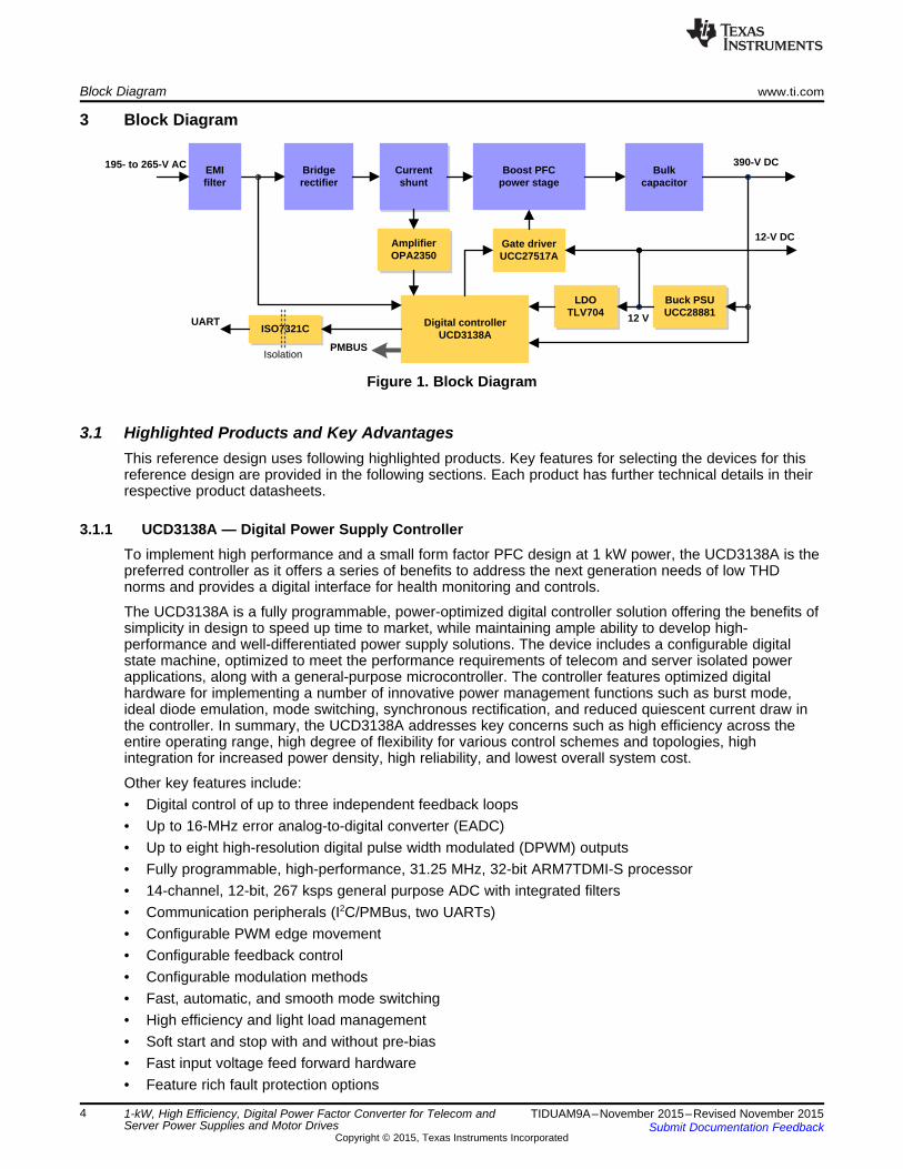
Digital controller UCD3138A
Boost PFC power stage
EMI filter
Bridge rectifier
195- to 265-V AC 390-V DC
12 V
Bulk capacitor
Buck PSU UCC28881
Gate driverUCC27517A
Current shunt
Amplifier OPA2350
LDO TLV704
ISO7321C
PMBUS
UART
12-V DC
Isolation
TI Designs1-kW, High Efficiency, Digital Power Factor Converter forTelecom and Server Power Supplies and Motor Drives
TI Designs Design FeaturesTIDA-00477 is a 1-kW (1000 W) power factor • Wide Operating Input Range: 195-V to 270-V ACconverter (PFC) designed for telecom, server, and • Designed to Drive Wide Range of Downstreamindustrial power supplies, and motor drives. This DC/DC Converters and Inverter-Fed Motors up toreference design presents a continuous conduction 1 kWmode boost converter, implemented using a
• High Power Factor > 0.99 and < 5% THD FromUCD3138A Digital Power Supply controller with allMedium-to-Full Load (50% to 100%); Meetsprotections built-in. Designed and tested hardwareCurrent THD Regulations as per IEC 61000-3-2meets or exceeds conducted emission, surge, and
• High Efficiency of > 97% at Full Load Over EntireEFT EN55014 requirements.Operating Voltage Range.Key highlights of this reference design:
• No Need for External Cooling up to 55°C Ambient• Provides a ready platform of front-end PFC toOperation for Loads ≤ 850 Waddress various power supplies and motor drives
up to 1 kW • Communicates Input Power ConsumptionInformation of the Unit Precisely for all Load• Improves overall system performance with lowerConditionsbus ripple, lower bus capacitance, lower RMS
currents, and front-end protections • Built-in 12-V/3-W Supply for Housekeeping PowerNeeds• Meets stringent current THD and power factor
norms • PMBUS and Isolated UART for Communication• Protects for output overcurrent, overvoltage, and • Meets the Requirements of Conducted Emissions
undervoltage conditions Standard – EN55011 Class A, EFT Norm IEC6000-4-4, and Surge Norm IEC61000-4-5Design Resources
• PFC Converter Designed With a Simple, SmallPCB Form Factor (165 × 95 mm)Design FolderTIDA-00477
UCD3138A Product Folder Featured ApplicationsUCC28881 Product Folder
• Telecom RectifiersUCC27517A Product Folder• Server and Industrial Power SuppliesTLV704 Product Folder
OPA2350 Product Folder • Online UPSISO7321C Product Folder • Power Storage Banks
• Motor Drives
ASK Our E2E Experts
1TIDUAM9A–November 2015–Revised November 2015 1-kW, High Efficiency, Digital Power Factor Converter for Telecom and ServerPower Supplies and Motor DrivesSubmit Documentation Feedback
Copyright © 2015, Texas Instruments Incorporated

Key System Specifications www.ti.com
An IMPORTANT NOTICE at the end of this TI reference design addresses authorized use, intellectual property matters and otherimportant disclaimers and information.
1 Key System Specifications
Table 1. Key System Specifications
PARAMETER SPECIFICATIONSInput voltage range 195 to 270-V AC (230-V nominal hi-line bus)
Input supply frequency 47 to 63 HzOutput voltage 390-V DCOutput power 1000 W, 390 V at 2.56 A
Efficiency > 97%Power Factor > 0.99
Output overcurrentOutput overvoltage
ProtectionOutput undervoltageOpen-loop detection
Line and load regulation < ± 0.5%Operating ambient –10°C to 55°C
Board form factor, specs 165 × 95 mm ; PCB type: FR4, two layersConducted emissions As per EN55011 / EN55022 Class APower line harmonics As per IEC 61000-3-2 Class A
EFT As per IEC-61000-4-4Surge As per IEC-61000-4-5
2 1-kW, High Efficiency, Digital Power Factor Converter for Telecom and TIDUAM9A–November 2015–Revised November 2015Server Power Supplies and Motor Drives Submit Documentation Feedback
Copyright © 2015, Texas Instruments Incorporated

www.ti.com System Description
2 System DescriptionThe power supplies for telecom, server, and industrial systems convert AC line power to isolated constantDC voltage of –48 V in telecom systems, 12 V in server systems, and 24 V in industrial systems. Thesesystems are typical of high power ranging from 1 to 5 kW. These power supplies need a front-end powerfactor correction circuit to shape the input current of the power supply, to meet the power factor, andmatch current THD norms such as IEC61000-2-3.
A power factor correction (PFC) circuit shapes the input current of the power supply to be in phase withthe mains voltage and maximizes the real power drawn from the mains. In addition, PFC front end offersseveral benefits:• Reduces RMS input current
A power circuit with a 230-V/5-A rating is limited to about 575 W of available power with a PF of 0.5.Increasing the PF to 0.99 will double the deliverable power to 1138 W, allowing higher-power loads tobe operated.
• Facilitates power-supply holdupThe active PFC circuit maintains a fixed intermediate DC bus voltage independent of the input voltage,so the energy stored in the system does not decrease as the input voltage decreases. This allows useof smaller, cheaper bulk capacitors.
• Improves efficiency of downstream convertersPFC reduces the dynamic voltage range applied to downstream inverters and converters, reducingvoltage ratings of rectifiers that results in lower forward drops, and increasing operating duty-cyclescausing lower current in switches.
• Increases the efficiency of the power-distribution systemA lower RMS current reduces distribution wiring losses.
• Reduces the VA rating of standby power generators and stresses on neutral conductorsReducing harmonics eliminates the risk of triplen harmonics (the third and multiples thereof) that canamount to dangerous levels in the neutral conductor of Y-connected 3-phase systems.
This reference design uses a UCD3138A PFC controller to implement a boost power factor converter foruse in telecom, sever, and industrial systems that demand a PFC up to 1 kW. The design provides aready platform of active front end to operate downstream DC/DC converters or inverters operating on Hi-line AC voltage range from 195-V to 270-V AC.
Telecom, server, and industrial power supplies and motor drives require high efficiency over their entireoperating voltage range and wide load variations from 50% to 100% load. This design demonstrates ahigh performance power factor stage in a small form factor (165 × 95 mm), operating from 195-V to 270-VAC and delivers up to 1 kW of continuous power output at greater than 97% efficiency. The design alsoprovides precise information on power consumption of the end equipment from the AC input line, whichcan be used for energy calculations and control the load for power optimization on need basis.
The EMI filter at the front end of the circuit meets EN55011 class-A conducted emission levels. Thedesign meets control circuit needs and drives a small DC fan for cooling by using a built-in housekeeping2.5-W power supply. The design implements a low-frequency pulse-skipping techniques to regulate theDC bus during no load conditions (achieving very low standby power consumption). The design fully testsand validates for parameters such as regulation, efficiency, EMI signature, output ripple, startup, andswitching stresses.
The design meets the key challenges of telecom, server, and industrial power supplies and motor drives toprovide safe and reliable power with all built-in protections while delivering high performance with lowpower consumption and a low bill-of-material (BOM) cost.
3TIDUAM9A–November 2015–Revised November 2015 1-kW, High Efficiency, Digital Power Factor Converter for Telecom andServer Power Supplies and Motor DrivesSubmit Documentation Feedback
Copyright © 2015, Texas Instruments Incorporated
Digital controller UCD3138A
Boost PFC power stage
EMI filter
Bridge rectifier
195- to 265-V AC 390-V DC
12 V
Bulk capacitor
Buck PSU UCC28881
Gate driverUCC27517A
Current shunt
Amplifier OPA2350
LDO TLV704
ISO7321C
PMBUS
UART
12-V DC
Isolation
Block Diagram www.ti.com
3 Block Diagram
Figure 1. Block Diagram
3.1 Highlighted Products and Key AdvantagesThis reference design uses following highlighted products. Key features for selecting the devices for thisreference design are provided in the following sections. Each product has further technical details in theirrespective product datasheets.
3.1.1 UCD3138A — Digital Power Supply ControllerTo implement high performance and a small form factor PFC design at 1 kW power, the UCD3138A is thepreferred controller as it offers a series of benefits to address the next generation needs of low THDnorms and provides a digital interface for health monitoring and controls.
The UCD3138A is a fully programmable, power-optimized digital controller solution offering the benefits ofsimplicity in design to speed up time to market, while maintaining ample ability to develop high-performance and well-differentiated power supply solutions. The device includes a configurable digitalstate machine, optimized to meet the performance requirements of telecom and server isolated powerapplications, along with a general-purpose microcontroller. The controller features optimized digitalhardware for implementing a number of innovative power management functions such as burst mode,ideal diode emulation, mode switching, synchronous rectification, and reduced quiescent current draw inthe controller. In summary, the UCD3138A addresses key concerns such as high efficiency across theentire operating range, high degree of flexibility for various control schemes and topologies, highintegration for increased power density, high reliability, and lowest overall system cost.
Other key features include:• Digital control of up to three independent feedback loops• Up to 16-MHz error analog-to-digital converter (EADC)• Up to eight high-resolution digital pulse width modulated (DPWM) outputs• Fully programmable, high-performance, 31.25 MHz, 32-bit ARM7TDMI-S processor• 14-channel, 12-bit, 267 ksps general purpose ADC with integrated filters• Communication peripherals (I2C/PMBus, two UARTs)• Configurable PWM edge movement• Configurable feedback control• Configurable modulation methods• Fast, automatic, and smooth mode switching• High efficiency and light load management• Soft start and stop with and without pre-bias• Fast input voltage feed forward hardware• Feature rich fault protection options
4 1-kW, High Efficiency, Digital Power Factor Converter for Telecom and TIDUAM9A–November 2015–Revised November 2015Server Power Supplies and Motor Drives Submit Documentation Feedback
Copyright © 2015, Texas Instruments Incorporated

www.ti.com Block Diagram
• Internal temperature sensor• Timer capture with selectable input pins• Up to five additional general purpose timers• Built-in watchdog: BOD and POR• Operating temperature: –40°C to 125°C
3.1.2 UCC27517A — Low-Side Gate DriverLower switching losses are necessary to achieve high efficiency. The switching losses of a MOSFET are afunction of drive current that needs to pass quickly through the Miller Plateau Region of the power-MOSFET's switching transition. A high-current gate driver placed closely to FET helps achieve faster turnon and turn off by effectively charging and discharging voltage across its gate-to-drain parasitic capacitor(CGD), thus reducing switching losses effectively.
The UCC27517A is a simple, low-cost, low-side gate-driver device, which offers superior replacement ofstandard NPN and PNP discrete solutions with peak-source and sink current of 4 A. The device is asingle-channel high-speed gate driver and has symmetrical drive with negative input voltage handling (–5V) ability. The UCC27517A operates over a wide VDD range of 4.5 to 18 V and wide temperature range of–40°C to 140°C.
Other key features include:• Fast propagation delays (13 ns typical)• Outputs held low during VDD UVLO (ensures glitch-free operation at power up and power down)• Hysteretic-logic thresholds for high-noise immunity• Output held low when input pins are floating• 5-pin DBV (SOT-23) package helps to optimize the space
3.1.3 UCC28881 — 700-V Lowest Quiescent Current Off-Line SwitcherWith an integrated 700-V power MOSFET, current sensing, and eliminating bias winding, the UCC28881offers an easy to use AC/DC solution with minimal external component count and ideal device for lowwattage in-house power supplies due to its unique built-in features. The key values of the UCC28881solution are low quiescent power consumption, low component count, and robust operation with load shortand inductor runaway protection.
Other key features include:• Integrated 700-V start-up current source and power MOSFET• < 100-µA IC quiescent current• Self-biased switcher: Start-up and operation bias directly from rectified mains voltage• No external current sense resistor• Robust performance with load short and inductor current runaway• Soft start and thermal shutdown
3.1.4 TLV704 — 24-V Input Voltage, 150-mA, Ultralow IQ Low-Dropout RegulatorsTo optimize no load power loss and meet the control circuit power needs, the low dropout (LDO) linearregulator TLV704 is selected. The TLV704 operates over a wide input voltage range of 2.5 to 24 V andprovides 2% typical accuracy. The device is stable with an effective capacitance of 0.47 µF. This makesthe TLV704 an ideal solution for always on systems, which require very little idle state power dissipation.
Other key features include:• Current output up to 150 mA• Low power IQ = 3.2 µA
5TIDUAM9A–November 2015–Revised November 2015 1-kW, High Efficiency, Digital Power Factor Converter for Telecom andServer Power Supplies and Motor DrivesSubmit Documentation Feedback
Copyright © 2015, Texas Instruments Incorporated

Block Diagram www.ti.com
3.1.5 OPA2350 — High-Speed, Single-Supply, Rail-to-Rail Operational AmplifierAn operational amplifier (op amp) strengthens signals to accommodate the measurement range of theUCD3138 for current sensing feedback. The op amp should have sufficient bandwidth and rail-to-railoperation for exact detection of current sense feedback. This design requires a low-noise, rail-to-railswing, high-speed op amp, so the OPA2350 is selected. The features of the OPA2350 make it ideal fordriving sampling ADCs used for control loops. In addition, the amplifier’s wide operating temperaturerange and wide common-mode range ensures device performance in the most demanding environments.
Other key features include:• Rail-to-rail input and output• Wide bandwidth: 38 MHz• High slew rate: 22 V/µs• Low noise: 5 nV/√Hz• Single supply operation: As low as 2.5 V• Wide common-mode range
3.1.6 ISO7321C — Low-Power, Dual-Channel 1/1 Digital Isolator With Fail-Safe HighFor isolated communication interface dual channel isolator, the ISO7321C is the preferred choice, as itprovides up to 3000 VRMS for 1 minute per UL 1577. The device is capable of operating up to 25 Mbps andhas an integrated glitch filter to aid in low-frequency operation. In fail-safe condition, the ISO7321C outputdefaults to high level.
Other key features include:• Low power consumption, Typical ICC per channel at 1 Mbps: 1 mA (3.3-V supply)• Qualified for:
– IEC 61000-4-2 Level 3 ESD at 6 kV– IEC61000-4-4 Level 4 EFT at 4-kV Power, 4-kV I/O– IEC 61000-4-5 Level 4 Surge at 6 kV (Air), 8 kV (Oil)
• Wide temperature range: –40°C to 125°C
6 1-kW, High Efficiency, Digital Power Factor Converter for Telecom and TIDUAM9A–November 2015–Revised November 2015Server Power Supplies and Motor Drives Submit Documentation Feedback
Copyright © 2015, Texas Instruments Incorporated

www.ti.com System Design Theory
4 System Design TheoryThis reference design is a 1-kW boost power factor converter, operating in continuous conduction mode(CCM) and implemented using the UCD3138A Digital Power Supply controller. The design is specificallytailored for telecom, server, and industrial power supplies and motor drives. This serves as a superioralternative to existing analog control based PFC circuits used to meet the power harmonic norms. Thisdesign is intended for operation at country specific line voltages between 195-V to 265-V AC. Under fullload conditions, the system has greater than 97% efficiency over the wide input operating voltage rangefrom 195-V to 270-V AC. The design includes several embedded protections, which include outputovervoltage protection and output short-circuit protection. In addition, the design provides preciseinformation of the power consumption of the unit.
The main focus of this design is a low EMI, high efficiency, high power factor, and protected DC power railfor targeted applications.
4.1 PFC Regulator Operating ModeThe PFC shapes the input current of the power supply to maximize the real power available from themains. The PFC must also comply with low harmonic (low THD) regulatory requirements such asIEC61000-3-2. Currently, two modes of operation have been widely used for PFC implementations: CCMand critical conduction mode (CrM). For higher power circuits, the topology of choice is the boostconverter operating in CCM and with average current mode control. For lower power applications, the CrMboost topology is typically used.
For high power levels such as 1 kW, CCM operation is preferred as it has a lower peak and RMScurrents. Lower peak currents significantly reduce the stress in power MOSFET, diode, and inductor. Inaddition, filtering is easier because the current is more continuous through the boost inductor. Finally, theswitching frequency remains constant for the CCM operation, so the boost inductor design and EMI filterdesigns are easier.
4.2 PFC Circuit Component DesignThe UCD3138A is configured for fixed frequency in CCM and requires minimal external components forhigh wattage PFC regulator implementation. The following sections illustrate the design process andcomponent selection for this design.
4.2.1 Design Goal ParametersTable 2 shows the design goal parameters for this design. These parameters are used in furthercalculations for the selection of components.
Table 2. Design Goal Parameters
PARAMETER MIN TYP MAX UNITINPUT
VIN Input voltage 195 270 VAC
fLINE Input frequency 47 63 HzOUTPUT
VOUT Output voltage 390 VDC
POUT Output power 1000 WLine regulation 5%Load regulation 5%
PF Targeted power factor 0.99η Targeted efficiency 96%
7TIDUAM9A–November 2015–Revised November 2015 1-kW, High Efficiency, Digital Power Factor Converter for Telecom andServer Power Supplies and Motor DrivesSubmit Documentation Feedback
Copyright © 2015, Texas Instruments Incorporated

BRIDGEP 2 0.85 V 4.86 A 8.26 W= ´ ´ =
BRIDGE AVG(max)BRIDGE F INP 2 V I= ´ ´
IN_ AVG(max)
2I 7.63 A 4.86 A= ´ =
p
IN_ AVG(max) IN(max)
2I I= ´
p
IN(max)I 2 5.40 A 7.63 A= ´ =
IN(max) IN_RMS(max)I 2 I= ´
IN_RMS(max)
1000 WI 5.40 A
0.96 195 V 0.99= =
´ ´
OUT(max)IN_RMS(max)
IN(min)
PI
V PF=
h´ ´
OUT(max)
1000 WI 2.56 A
390 V= =
OUT(max)OUT(max)
OUT
PI
V=
System Design Theory www.ti.com
4.2.2 Current CalculationsThe input fuse, bridge rectifier, and input capacitor are selected based upon the input current calculations.First, determine the maximum average output current, IOUT(max):space
space
(1)
The maximum input RMS line current (IIN_RMS(max)) is calculated using the parameters from Table 2 and theefficiency and power factor initial assumptions:
space
(2)
The maximum input current (IIN(max)) and the maximum average input current (IIN_AVG(max)) can be determinedbased upon the calculated RMS value and assuming the waveform is sinusoidal:
space
(3)space
space
(4)
4.2.3 Bridge RectifierThe maximum input AC voltage is 270-V AC, so the DC voltage can reach voltage levels of up to 385-VDC. Considering a safety factor of 30%, select a component with voltage rating greater than 500-V DC.The input bridge rectifier must have an average current capability that exceeds the input average current(IIN_AVG(max)). A higher current bridge rectifier optimizes the power loss due to diode forward voltage drop.
This design uses a 1000-V, 15-A diode GBJ1508 for input rectification.
Forward voltage drop of bridge rectifier diode, VF_BRIDGE = 0.85 V
The power loss in the input bridge (PBRIDGE) can be calculated as:
space
(5)
Select an appropriately sized heat sink to maintain the safe operating area of the bridge rectifier.
8 1-kW, High Efficiency, Digital Power Factor Converter for Telecom and TIDUAM9A–November 2015–Revised November 2015Server Power Supplies and Motor Drives Submit Documentation Feedback
Copyright © 2015, Texas Instruments Incorporated

IN
3.05 AC 0.69 F
8 100 kHz 5.52 V= = m
´ ´
RIPPLEIN
SW IN_RIPPLE
IC
8 f V=
´ ´
IN_RIPPLEV 0.02 ( 2 195 V) 5.52 V= ´ ´ =
IN_RIPPLE RIPPLE _IN IN_RECTIFIED(min)V V V= D ´
RIPPLEI 0.4 (7.63 A) 3.05 A= ´ =
RIPPLE RIPPLE IN(max)I I I= D ´
www.ti.com System Design Theory
4.2.4 Inductor Ripple CurrentThe TIDA-00477 operates best in CCM. If the chosen inductor allows a relatively high-ripple current, theconverter will be forced to operate in Discontinuous Mode (DCM) at light loads and at the higher inputvoltage range. High-inductor ripple currents have an impact on the boundary of CCM and DCM andresults in higher light-load THD. This also affects the choices for the input capacitor, current sense resistor(RSENSE), and internal compensation values tuned in the software of the UCD3138A. Allowing an inductorripple current (ΔIRIPPLE) of 20% or less will result in CCM operation over the majority of the operating rangebut requires a boost inductor that has a higher inductance value and the inductor itself will be physicallylarge. In this design, the inductor size has a 40% peak to peak ripple current to optimize performance withsize and cost. The focus of the design minimizes space with the understanding that the converter operatesin DCM at the higher input voltages and at light loads but is optimized well for a nominal input voltage of230-V AC at full load.
4.2.5 Input CapacitorSelect the input capacitor based on the input ripple current and an acceptable high frequency inputvoltage ripple. Allowing an inductor ripple current (ΔIRIPPLE) of 40% and a high frequency voltage ripplefactor (ΔVRIPPLE_IN) of 2%, the maximum input capacitor value (CIN) is calculated by first determining theinput ripple current (IRIPPLE) and the input voltage ripple, VIN_RIPPLE:
space
(6)
TEXT
space
(7)
The recommended value for the input X-capacitor can now be calculated as:
space
(8)
A standard value 1.0-µF X2 film capacitor is used.
9TIDUAM9A–November 2015–Revised November 2015 1-kW, High Efficiency, Digital Power Factor Converter for Telecom andServer Power Supplies and Motor DrivesSubmit Documentation Feedback
Copyright © 2015, Texas Instruments Incorporated

DIODEP 1.5 V 2.56 A 0.5 100 kHz 390 V 13 nC 4.09 W= ´ + ´ ´ ´ =
DIODE F _125 C OUT(max) SW OUT RRP V I 0.5 f V Q= ´ + ´ ´ ´
DIODEP 1.25 V 2.56 A 0.5 100 kHz 390 V 0 nC 3.20 W= ´ + ´ ´ ´ =
(max)
390 V (1.414 195 V)DUTY 0.293
390 V
- ´
= =
OUT IN_RECTIFIED(min)(max)
OUT
V VDUTY
V
-
=
BST(min)
390 V 0.5 (1 0.5)L 319 H
(100 kHz 3.05 A)
´ ´ -³ ³ m
´
OUTBST(min)
SW RIPPLE
V D (1 D)L
f I
´ ´ -
³
´
L _PEAK (max)
3.05 AI 7.63 A 9.155 A
2= + =
RIPPLEL _PEAK (max) IN(max)
II I
2= +
System Design Theory www.ti.com
4.2.6 Boost InductorBased upon the allowable inductor ripple current discussed previously, select the boost inductor (LBST)after determining the maximum inductor peak current, IL_PEAK:
space
(9)
Calculate the minimum value of the boost inductor based upon the acceptable ripple current (IRIPPLE) at aworst case duty cycle of 0.5:
space
(10)
The actual value of the boost inductor used is LBST = 320 µH.
The duty cycle of operation is a function of the rectified input voltage and will continuously change overthe half line cycle. Calculate the duty cycle (DUTY(max)) at the peak of minimum input voltage:
space
(11)
4.2.7 Boost DiodeThe output diode must have a blocking voltage that exceeds the output overvoltage of the converter andaverage current same as IOUT(max). The diode is generally an ultra-fast recovery diode or a silicon carbideSchottky diode.
For high wattages such as 1 kW, using a silicon carbide Schottky diode, although more expensive, willeliminate the reverse recovery losses and result in less power dissipation. Select the C3D04060A, 600-V/7.5-A SiC diode, as the output diode.
The estimated power loss with SiC diode is VF_125C = 1.25 V; QRR = 0.(12)
If an ultra-fast diode is preferred over a silicon carbide Schottky diode, select the BYV29FX-600, a 600-V/9-A diode, for this design. Estimate the diode losses with ultra-fast diodes based on the forward voltagedrop (VF) at 125°C and the reverse recovery charge (QRR) of the diode:
space
(13)
Use an appropriately sized heat sink for the boost diode.
10 1-kW, High Efficiency, Digital Power Factor Converter for Telecom and TIDUAM9A–November 2015–Revised November 2015Server Power Supplies and Motor Drives Submit Documentation Feedback
Copyright © 2015, Texas Instruments Incorporated

COND SWP P 3.884 3.588 7.472 W+ = + =
2SWP 100 kHz 0.5 390 V 7.63 A (12 ns 9 ns) 0.5 61pF 390 V 3.588 Wé ù= ´ ´ ´ ´ + + ´ ´ =
ë û
2SW SW OUT IN(max) r f OSS OUT
P f 0.5 V I (t t ) 0.5 C Vé ù= ´ ´ ´ + + ´ ´ë û
2CONDP 3.24 A (0.37 ) 3.884 W= ´ W =
2COND DS(on)DS _RMS
P I R= ´
DS _RMS
1000 W 16 275 VI 2 3.24 A
275 V 3 390 V
æ ö´= ´ - =ç ÷
´ p ´è ø
OUT(max) IN_RECTIFIED(min)DS _RMS
IN_RECTIFIED(min) OUT
P 16 VI 2
V 3 V
´
= ´ -
´ p ´
www.ti.com System Design Theory
4.2.8 Switching ElementA UCC27517A gate driver drives the MOSFET switch for which VCC bias voltages are limited to less than12 V from the bias supply. Use an external gate drive resistor to limit the rise time and to dampen anyringing caused by the parasitic inductances and capacitances of the gate drive circuit; this will meet anyEMI requirements of the converter. This design uses a 5.0-Ω resistor; the final value of any design isdependent upon the parasitic elements associated with the layout of the design. To facilitate a fast turnoff,a standard 100-V, 1-A Schottky diode or switching diode is placed anti-parallel with the gate drive resistor.Place a 10-kΩ resistor between the gate of the MOSFET and ground to discharge the gate capacitanceand protect from inadvertent dv/dt triggered turn on.
Calculate the drain to source RMS current (IDS_RMS) through switching FET by using the followingequations:
space
(14)
The maximum voltage across the FET is the maximum output boost voltage (that is, 420 V), which is theovervoltage set point of the PFC converter to shut down the output. Considering a derating of 30%, thevoltage rating of the MOSFET should be greater than 550-V DC.
Select the IPP60R190P6 MOSFET of 600 V and 25 A at 25°C / 12 A at 100°C for the current design.
Estimate the conduction losses of the switch MOSFET in this design using the RDS(on) at 125°C, found inthe device datasheet, and the calculated drain to source RMS current, IDS_RMS:
space
(15)
Estimate the switching losses using the rise time, tr, and fall time, tf, of the MOSFET gate, and the outputcapacitance losses, COSS:
space
(16)
Total FET losses:(17)
Use an appropriately sized heat sink for the MOSFET.
11TIDUAM9A–November 2015–Revised November 2015 1-kW, High Efficiency, Digital Power Factor Converter for Telecom andServer Power Supplies and Motor DrivesSubmit Documentation Feedback
Copyright © 2015, Texas Instruments Incorporated

2
RSENSEP 5.40 A 0.008 0.233 W= ´ W =
2RSENSE SENSEIN_RMS(max)
P I R= ´
2.00k
R25
2.00k
R24
42.2kR27
1
3
2
D9
SGND
1
3
2
D10
+3.3VA
+3.3VA
1
3
2
48
U3AOPA2350
0.1µFC22
0
R34
42.2k
R26
D17
+3.3VA
270pF
C20
270pFC19
I
1.6 VK 21.84
7.63 A 1.2 0.008£ =
´ ´ W
IIN(max) SENSE
1.6 VK
I 1.2 R£
´ ´
System Design Theory www.ti.com
4.2.9 Sense ResistorSelect a current sense resistor based on two key parameters:• Optimizing the power loss in the circuit• Requiring gain and bandwidth of the op amp used to amplify the current sense signal
For current sensing feedback, the OPA2350 strengthens the signals and accommodates the signal rangewithin the measurement range of the UCD3138. In the UCD3138, the ADC used from current sensing hasthe measurement range of 0 to 1.6 V and has the analog comparator range of 0 to 2.5 V. To have thebest signal-to-noise ratio and maximum input signal corresponding to overcurrent condition, RSENSEselected is 0.008 Ω.
For the signal conditioning, each input signal should follow the subsequent guidelines to limit the amplifiedsignal within the range of ADC previously mentioned. The maximum op amp gain is defined by:
(18)
In Equation 18, a factor of 20% is taken for the overcurrent limit.
Set a gain of 21.1 using resistors R24 and R26 across the current sense amplifier, U3, as shown in .
Figure 2. Sense Resistor Schematic
Calculate the power dissipated across the sense resistor, PRSENSE:
space
(19)
12 1-kW, High Efficiency, Digital Power Factor Converter for Telecom and TIDUAM9A–November 2015–Revised November 2015Server Power Supplies and Motor Drives Submit Documentation Feedback
Copyright © 2015, Texas Instruments Incorporated

2 2COUT _RMS(total)I (1.81 A) (2.43 A) 3.03 A= + =
2 2COUT _RMS(total) COUT _ 2 fline COUT _HFI (I ) (I )= +
COUT _HF
16 390 VI 2.31 A 1.5 2.43 A
3 1.414 195 V
´
= ´ - =
´ p ´ ´
OUTCOUT _HF OUT(max)
IN_RECTIFIED(min)
16 VI I 1.5
3 V
´
= ´ -
´ p ´
COUT _ 2 fline
2.56 AI 1.81 A
2= =
OUT(max)COUT _ 2 fline
II
2=
OUT(max)OUT _RIPPLE(pp)
LINE(min) OUT
IV
2 2 f C=
p ´ ´ ´
OUT(max)OUT _RIPPLE(pp)
LINE(min) OUT
IV
2 2 f C=
p ´ ´ ´
OUT _RIPPLE(pp) PPV 0.05 390 V 19.5 V< ´ =
OUT _RIPPLE(pp) OUTV 0.05 V< ´
OUT(min) 2 2
2 1000 W 21.3 msC 578 F
(390 V 280 V)
´ ´´ = m
-
OUT(max) HOLDUPOUT(min) 2 2
OUT OUT _HOLDUP(min)
2 P tC
V V
´ ´
³
-
www.ti.com System Design Theory
4.2.10 Output CapacitorSize the output capacitor, COUT, to meet holdup requirements of the converter. Assuming the downstreamconverters require the output of the PFC stage to always remain above 280-V DC (VOUT_HOLDUP(min)) duringone line cycle (tHOLDUP = 1 / fLINE(min)), the minimum calculated value for the capacitor is:
space
(20)
De-rate this capacitor value by 10%; the actual capacitor used is 660 µF.
To avoid triggering the output overvoltage or undervoltage protection features of the controller, verify thatthe maximum peak-to-peak output ripple voltage will be less than 5% of the output voltage. If the outputripple voltage is greater than 5% of the regulated output voltage, a larger output capacitor is required. Themaximum peak-to-peak ripple voltage, occurring at twice the line frequency, and the ripple current of theoutput capacitor is calculated:
space
(21)space
space
(22)
The required ripple current rating at twice the line frequency is equal to:
space
(23)
A high frequency ripple current through the output capacitor exists:
space
(24)
Select the output capacitor based on the total ripple current in the output capacitor, calculated as follows:
space
(25)
13TIDUAM9A–November 2015–Revised November 2015 1-kW, High Efficiency, Digital Power Factor Converter for Telecom andServer Power Supplies and Motor DrivesSubmit Documentation Feedback
Copyright © 2015, Texas Instruments Incorporated

FB2 FB1
2.0 VR R 3.07 k
390 V= ´ = W
REF FB1
FB2
OUT REF
V RR
V V
´
=
-
V OUT
2.5 VK 0.00595
420 V£ =
V OUTOUT(max)
2.5 VK
V£
System Design Theory www.ti.com
4.2.11 Output Voltage Set PointFor low power dissipation and minimal contribution to the voltage set point, use 600 kΩ for the top voltagefeedback divider resistor, RFB1. Use multiple resistors in series due to the maximum allowable voltageacross each resistor.
For each input signal to the UCD3138, the magnitude accommodates the measurement range of thedevice. In the UCD3138, the ADC measurement range is 0 to 2.5 V. To have the best signal-to-noiseratio, maximize the input signal. For this reason, the signal conditioning for each input signal must followthese guidelines:
For VOUT, the voltage divider:
(26)
When the maximum output voltage VOUTMAX is 420-V DC, including the overvoltage protection set at 415-VDC:
Considering the above constraints on the gain, select the bottom divider resistor, RFB2, to meet thefeedback voltage of 2.0 V at VOUT of 390 V.
space
(27)
Select a standard value 3.16 kΩ resistor for RFB2.
Add a 0.1-µF capacitor across RFB2 to filter out noise.
14 1-kW, High Efficiency, Digital Power Factor Converter for Telecom and TIDUAM9A–November 2015–Revised November 2015Server Power Supplies and Motor Drives Submit Documentation Feedback
Copyright © 2015, Texas Instruments Incorporated

www.ti.com System Design Theory
4.3 Bias PowerAn auxiliary housekeeping power supply powers the UCD3138A control circuit, UCC27517A Gate Driver,and the inrush current limiting bypass relay. In addition, when the converter operates at power greaterthan or equal to 850 W, external cooling is required. To meet each need, the board produces an auxiliarypower supply of 2.5 W using a low quiescent current, high voltage off-line switcher UCC28881. Thisdevice, including the integrated 700 V Power MOSFET, offers a low part count and a relatively low costsolution for implementing buck regulator to generate bias power.
The PFC pre-regulator output stage powers a buck converter and must start up prior to the PFC stagebeing operational. Therefore, design the circuit to operate over a wide input (100-V to 450-V DC) voltage.The buck converter output is designed for 12 V and 250 mA of current to meet the following power needs:
Table 3. Power Needs
DEVICE VOLTAGE (V) MAX CURRENT (mA)UCD3138A controller 3.3 100Relay 12 35Gate Driver 12 35Fan (optional) 12 75
The application and implementation section of the UCC28881 datasheet explains the design of powerstage components (output filter inductor, output filter capacitor, and feedback circuitry).
4.4 Designing the Firmware on UCD3138A Controller for Single-Phase PFCThe UCD3138 digital power supply controller has multiple peripherals inside the device, which have beenspecifically optimized to enhance the performance of PFC circuit.
A step-by-step guide for the design of the UCD3138A firmware required for the TIDA-00477 PFC isexplained in the PMP10804 Test Results (TIDUAY4).
The document covers the hardware interface, voltage loop and current loop implementation, systemprotection, firmware structure, internal state machines, and other advanced features. Finally, a graphicaluser interface (GUI) and a guide for tuning the coefficients of a PFC system are presented.
15TIDUAM9A–November 2015–Revised November 2015 1-kW, High Efficiency, Digital Power Factor Converter for Telecom andServer Power Supplies and Motor DrivesSubmit Documentation Feedback
Copyright © 2015, Texas Instruments Incorporated

Getting Started Firmware www.ti.com
5 Getting Started FirmwareThis section details the necessary equipment, test setup, and procedure instructions for the TIDA-00477board programming with provided software.
5.1 Programming the UCD3138AEquipment and necessary files needed for programming the device:• PMBus to USB Interface Adapter Kit: The USB Interface Adapter (HPA172)
Accessories include:– USB interface adapter– USB cable (5-pin B Mini Male to Type A Male)– Ribbon cable (Socket to Socket, 10-pin, 2 headers, polarized)
Figure 3. USB Adapter (HPA172) Outlook
• GUI installations file "TI-Fusion-Digital-Power-Designer-2.0.16.exe" or later version.• Firmware File TIDCAX3_TIDA-00477_Program_V1.x0.• PC computer operating system: Microsoft® Windows® XP®, or Vista®, or Windows 7®.
16 1-kW, High Efficiency, Digital Power Factor Converter for Telecom and TIDUAM9A–November 2015–Revised November 2015Server Power Supplies and Motor Drives Submit Documentation Feedback
Copyright © 2015, Texas Instruments Incorporated

www.ti.com Getting Started Firmware
5.1.1 Equipment Setup (GUI)
1. Find Installation FileThe GUI installation file is "TI-Fusion-Digital-Power-Designer-Version-2.0.16.exe" or later version.
2. Install the softwareDouble click and launch the ".exe" file to start the installation. Click "Next" until an agreement pageappears. After reading the agreement, click "I accept the agreement." Click "Install".
3. Launch UCD3138 Device GUIAfter the installation, click "Finish" to exit setup; then click "Exit Program". The GUI for the TIDA-00477board can be launched through the following steps:(a) Click the Windows "Start" button.(b) Click "All Programs".(c) Click "Texas Instruments Fusion Digital Power Designer".(d) Click "Device GUIs".(e) Click "UCD3xxx & UCD9xxx Device GUI".
Figure 4. GUI Launch Path
17TIDUAM9A–November 2015–Revised November 2015 1-kW, High Efficiency, Digital Power Factor Converter for Telecom andServer Power Supplies and Motor DrivesSubmit Documentation Feedback
Copyright © 2015, Texas Instruments Incorporated

Getting Started Firmware www.ti.com
5.1.2 Hardware SetupFigure 5 shows the connection between TIDA-00477 and the PC computer through a USB InterfaceAdapter (HPA172).
Figure 5. TIDA-00477 Setup for Programing UCD3138A
To connect the USB Adaptor:1. Connect one end of the ribbon cable to the TIDA-00477 board at connector J4 and connect the other
end to the USB interface adapter (HPA172).2. Connect the Mini connector of the USB cable to the USB interface adapter and connect the other end
to the USB port of the PC Computer.3. The LED on HPA172 should be illuminated. If not, un-plug the USB cable and reconnect. If the LED is
still not illuminated, change with a new HPA172 USB adapter. If the LED is illuminated, proceed to thenext step.
18 1-kW, High Efficiency, Digital Power Factor Converter for Telecom and TIDUAM9A–November 2015–Revised November 2015Server Power Supplies and Motor Drives Submit Documentation Feedback
Copyright © 2015, Texas Instruments Incorporated

www.ti.com Getting Started Firmware
5.1.3 Procedure
1. Launch the GUI by the steps described in Section 5.1.1. Wait until the Figure 6 window appears.2. Click "Scan Device in ROM Mode", then wait and check Figure 6 on its "Log" and confirm "Found ROM
v2 IC v3 – UCD31xx". If "Found ROM" does not show, take the following steps:(a) Click "Device ID".(b) Click "Command Program" to jump to ROM (sendByte0xD9).(c) Click "Scan Device in ROM Mode" again.If the device is detected, proceed to the next step.
Figure 6. OK Indication (Found ROM)
19TIDUAM9A–November 2015–Revised November 2015 1-kW, High Efficiency, Digital Power Factor Converter for Telecom andServer Power Supplies and Motor DrivesSubmit Documentation Feedback
Copyright © 2015, Texas Instruments Incorporated

Getting Started Firmware www.ti.com
3. On the GUI shown in Figure 6, click "Firmware Download". A new window appears, shown in Figure 7.In this new window:(a) Check "Download data flash".
If "DO NOT write program checksum" radio button is selected as in Figure 7, the firmware will notexecute once the PFC powers up.Click "Command ROM" to execute the program.spaceif "Write program checksum", radio button is selected, the firmware will execute automatically oncethe PFC powers up.
(b) Click "Select file".Find "TIDCAX3_TIDA-00477_Program_V1.x0".Click "Download".
(c) After the program downloads, click "Close" as shown in Figure 7.
Figure 7. Download Firmware
20 1-kW, High Efficiency, Digital Power Factor Converter for Telecom and TIDUAM9A–November 2015–Revised November 2015Server Power Supplies and Motor Drives Submit Documentation Feedback
Copyright © 2015, Texas Instruments Incorporated

www.ti.com Getting Started Hardware
6 Getting Started HardwareThis section details the necessary equipment, test setup, and procedure instructions to test and validatethe TIDA-00477 board.
6.1 Test ConditionsFor input, the power supply source (VIN) must range from 195-V to 270-V AC. Set the input current limit ofinput AC source to 7.5 A.
For output, use an electronic variable load or a variable resistive load, which must be rated greater than orequal to 400 V and must vary the load current from 0 mA to 3.0 A
6.2 Test Equipment Required for Board Validation• Isolated AC source• Single-phase power analyzer• Digital oscilloscope• Multimeters• Electronic load or resistive load
6.3 Test Procedure
1. Connect input terminals (Pin-1 and Pin-3 of connector J1) of the reference board to the AC powersource.
2. Connect output terminals (Pin-1 and Pin-3 of connector J2) to electronic load, maintaining correctpolarity. Pin-1 is V DC output and Pin-3 is GND terminal
3. Set and maintain a minimum load of about 10 mA.4. Increase the input voltage gradually from 0 V to turn on voltage of 195-V AC.5. Start the load to draw current from the output terminals of the PFC.6. Observe startup conditions for smooth switching waveforms.7. For power greater than or equal to 850 W, an external fan can be used for cooling. A low wattage, high
LFM fan such as 612NMLE is recommend for usage with 12 V output provided at connector J3. Ensurethat fan is rated for 12-V operation and power less than or equal to 0.5 W.
8. Connect the fan at connector J3, maintaining correct polarity.9. If low wattage fan is not available, a cooling fan can be powered from an external DC lab power
supply.
21TIDUAM9A–November 2015–Revised November 2015 1-kW, High Efficiency, Digital Power Factor Converter for Telecom andServer Power Supplies and Motor DrivesSubmit Documentation Feedback
Copyright © 2015, Texas Instruments Incorporated

Test Results www.ti.com
7 Test ResultsTest results are divided in multiple sections that cover the steady state performance, functionalperformance waveforms and test data, transient performance waveforms, thermal measurements,conducted emission measurements and surge and EFT measurements.
7.1 Performance Data
7.1.1 Efficiency and Regulation With Load VariationTable 4 shows the data at 230-V AC input:
Table 4. Efficiency and Regulation with Load 230-V AC Input
VINAC (V) IINAC (A) PF PINAC (W) iTHD (%) VOUT (V) IOUT (A) POUT (W) EFF (%) REG (%)230 0.19 0.57 24.20 26.00 390.70 0.05 20.30 83.90 –0.09230 0.26 0.76 45.40 16.90 391.30 0.10 40.10 88.50 0.07230 0.49 0.93 104.80 9.83 391.20 0.25 99.00 94.40 0.06230 0.91 0.98 204.50 6.25 391.20 0.50 196.80 96.30 0.05230 1.34 0.99 303.60 2.97 391.10 0.75 294.60 97.00 0.03230 1.77 0.99 403.20 2.19 391.10 1.00 392.10 97.30 0.01230 2.20 1.00 503.00 1.87 391.00 1.25 489.80 97.40 0.00230 2.63 1.00 603.30 1.80 390.90 1.50 587.70 97.40 –0.02230 3.07 1.00 703.80 1.59 390.90 1.75 685.60 97.40 –0.04230 3.51 1.00 804.40 1.47 390.80 2.01 783.60 97.40 –0.05230 3.92 1.00 899.50 1.50 390.80 2.24 875.40 97.30 –0.05230 4.47 1.00 1027.00 1.60 390.80 2.55 997.90 97.20 –0.05
7.1.2 Standby PowerThe standby power was noted at multiple AC input voltages with a constant negligible load on the outputDC bus and with the PFC controller enabled and disabled. The results are tabulated in Table 5 andTable 6:
Table 5. PFC Circuit ON: Load: Constant Current: 1.92 mA
NO LOADVINAC (V AC) IINAC(A) PINAC (W) VOUT (V) IOUT (A) POUT (W) POWER (W)195 0.100 4.62 391 0.002 0.75 3.87230 0.110 4.12 391 0.002 0.75 3.37270 0.124 3.87 391 0.002 0.75 3.11
Table 6. PFC Circuit OFF: Resistor R86 Removed (1)
NO LOADVINAC (VAC) IINAC(A) PINAC (W) VOUT (V) IOUT (A) POUT (W) POWER (W)195 0.095 2.88 275 0.001 0.37 2.51230 0.106 3.25 322 0.002 0.51 2.74270 0.122 3.55 381 0.002 0.71 2.84
(1) Resistor R86 removed to isolate PWM output of UCD to gate driver
Three main branches contribute no load power:• Input AC voltage sensing resistors• Output DC bus voltage sensing resistors• Buck regulator delivering power to controller, relay and gate driver
22 1-kW, High Efficiency, Digital Power Factor Converter for Telecom and TIDUAM9A–November 2015–Revised November 2015Server Power Supplies and Motor Drives Submit Documentation Feedback
Copyright © 2015, Texas Instruments Incorporated

Load Current (A)
Pow
er F
acto
r
0 0.3 0.6 0.9 1.2 1.5 1.8 2.1 2.4 2.70.8
0.85
0.9
0.95
1
1.05
D002
270-V AC230-V AC195-V AC
Load Current (A)
Effi
cien
cy
0 0.3 0.6 0.9 1.2 1.5 1.8 2.1 2.4 2.790%
91%
92%
93%
94%
95%
96%
97%
98%
99%
100%
D001
270-V AC230-V AC195-V AC
www.ti.com Test Results
Power loss contribution and reduction possibilities:• AC input and DC output sensing resistors consume approximately 0.55 W. Increasing resistor values
can decrease the power consumed by AC input and DC output sensing resistors.• LDO power loss used to power controller is approximately 0.87 W and by using a DC-DC converter to
converter 12-V bias to 3.3 V the power loss is mitigated.
7.2 Performance Curves
7.2.1 Efficiency and Power Factor With Load and Line VariationFigure 8 and Figure 9 show the measured efficiency and power factor in the system with AC input voltagevariation.
Figure 8. Efficiency Versus Output Load Current (IOUT)
Figure 9. Power Factor versus Load Current
23TIDUAM9A–November 2015–Revised November 2015 1-kW, High Efficiency, Digital Power Factor Converter for Telecom andServer Power Supplies and Motor DrivesSubmit Documentation Feedback
Copyright © 2015, Texas Instruments Incorporated

Load Current (A)
Reg
ulat
ion
0 0.3 0.6 0.9 1.2 1.5 1.8 2.1 2.4 2.7-0.2%
-0.15%
-0.1%
-0.05%
0
0.05%
0.1%
0.15%
0.2%
D004
270-V AC230-V AC195-V AC
Load Current (A)
TH
D
0 0.3 0.6 0.9 1.2 1.5 1.8 2.1 2.4 2.70
5%
10%
15%
20%
25%
D003
270-V AC230-V AC195-V AC
Test Results www.ti.com
7.2.2 Input THD With Load and Line RegulationFigure 10 shows the measured input THD of the system with AC input voltage variation.Figure 11 shows the measured load regulation of the output with AC input voltage variation.
Figure 10. Input THD Variation With Load Current
Figure 11. Output Voltage Variation With Load Current for Various AC Input Voltages
24 1-kW, High Efficiency, Digital Power Factor Converter for Telecom and TIDUAM9A–November 2015–Revised November 2015Server Power Supplies and Motor Drives Submit Documentation Feedback
Copyright © 2015, Texas Instruments Incorporated

www.ti.com Test Results
7.3 Functional Waveforms
7.3.1 Switching Node WaveformsThe waveform at switching (SW) node was observed along with the MOSFET current for 230-V AC and270-V AC under full load (2.31 A) conditions.
Figure 12. SW Node Waveform and MOSFET Current at Figure 13. SW Node Waveform Turnon Cycle at VINAC =VINAC= 230-V AC, Full Load 230-V AC, Full Load
Figure 14. SW Node Waveform Turnoff Cycle at VINAC= 230-V AC, Full Load
NOTE: Red trace: Drain voltage, 100 V/div; Green trace: Drain current, 5 A/div
25TIDUAM9A–November 2015–Revised November 2015 1-kW, High Efficiency, Digital Power Factor Converter for Telecom andServer Power Supplies and Motor DrivesSubmit Documentation Feedback
Copyright © 2015, Texas Instruments Incorporated

Test Results www.ti.com
7.3.2 Input Voltage and Current WaveformFigure 15 shows the input current waveform at 230-V AC with full load condition.
Figure 15. Input Voltage and Input Current at VINAC = 230-V AC, Full Load
26 1-kW, High Efficiency, Digital Power Factor Converter for Telecom and TIDUAM9A–November 2015–Revised November 2015Server Power Supplies and Motor Drives Submit Documentation Feedback
Copyright © 2015, Texas Instruments Incorporated

www.ti.com Test Results
7.3.3 Inrush Current WaveformInrush current drawn by the system is observed and recorded at maximum input voltage of 270-V AC.
Figure 16. Output Voltage and Input Inrush Current at VINAC = 270 V, Full Load
7.3.4 Output Ripple
Figure 17. Output Voltage Ripple at VINAC = 230 V, Full Figure 18. Output Voltage Ripple at VINAC = 230 V, FullLoad Load, Only 50-Hz Component
NOTE: Ripple observed at 390-V DC output loaded to 2.56 A at 230-V AC.
27TIDUAM9A–November 2015–Revised November 2015 1-kW, High Efficiency, Digital Power Factor Converter for Telecom andServer Power Supplies and Motor DrivesSubmit Documentation Feedback
Copyright © 2015, Texas Instruments Incorporated

Test Results www.ti.com
7.3.5 Turn-on CharacteristicsThe 390-V output turn on at full load (2.31 A) was recorded at 230-V AC.
Figure 19. Output Turn-on Waveform at VINAC = 230 V Figure 20. Output Turn-on Waveform at VINAC = 230 V,With Light Load of 0.5 A With Full Load of 2.56 A
NOTE: Red trace: Output DC bus, 100 V/div; Blue trace: Input voltage, 100 V/div.
7.4 Transient Waveforms
7.4.1 Transient Load ResponseObserved load transient performance with the load switched at a 0.2-m wire length. Switch the output loadusing electronic load.
VIN = 230-V AC, load transient from 0.5 to 2.56 A with vice-versa performance at 390 V output.
Figure 21. Output Voltage Waveform at VINAC = 230 V, Figure 22. Output Voltage Waveform at VINAC = 230 V,Load Transient From 0.5 to 2.56 A Load Transient From 2.56 to 0.5 A
NOTE: Red trace: Output voltage, 20 V/div, AC coupling; Green trace: Output current, 1 A/div.
28 1-kW, High Efficiency, Digital Power Factor Converter for Telecom and TIDUAM9A–November 2015–Revised November 2015Server Power Supplies and Motor Drives Submit Documentation Feedback
Copyright © 2015, Texas Instruments Incorporated

www.ti.com Test Results
7.5 Conducted EmissionsConducted emissions will generally be more at full load. Choose this operating point for measuring EMI.
7.5.1 With Resistive Load at OutputConnect the 230-V AC input, 2.56 A resistive load to the PSU using short leads. In a pre-compliance testsetup, the conducted emissions were compared against EN55011 class-A limits and found to meet theselimits satisfactorily.
Figure 23. Conducted Emissions per EN55011 Class A
29TIDUAM9A–November 2015–Revised November 2015 1-kW, High Efficiency, Digital Power Factor Converter for Telecom andServer Power Supplies and Motor DrivesSubmit Documentation Feedback
Copyright © 2015, Texas Instruments Incorporated

Test Results www.ti.com
7.6 Surge and Fast Transient TestPer EN55014, surge and EFT tests are completed on the boards. The test condition and test results aretabulated in Table 7:
Table 7. Surge and EFT Test Result
REQUIREMENTS OFIEC 61000-6-2/EN
50082-2: IMMUNITY PERFORMANCEBASIC STANDARD PORT TEST RESULTSTANDARD FOR CRITERION REQUIREDINDUSTRIAL
ENVIRONMENTSPassed withIEC/EN 61000-4-4: AC input ±2 kV, 5 kHz B (1) performance criterionEFT A (2)
Passed withIEC/EN 61000-4-5: ±4 kV line to earthAC input B (1) performance criterion ASurge ±2 kV line to line (2)
(1) Temporary loss of function or degradation of performance that ceases after the disturbance ceases(2) Normal performance within limits specified by the design/manufacturer
30 1-kW, High Efficiency, Digital Power Factor Converter for Telecom and TIDUAM9A–November 2015–Revised November 2015Server Power Supplies and Motor Drives Submit Documentation Feedback
Copyright © 2015, Texas Instruments Incorporated

195 to 265 VAC
GNDE
PGND
3.01
R5
390 VDC2.3 Amps max
TP1
TP6
0.68µFC1
10.0kR3
275VRV1
1.5µFC3
DNP
R28
DNP
C21
NOTES:LINE INPUT VOLTAGE: 195VRMS - 265VRMS, 47Hz - 63HzPEAK INPUT CURRENT: 7.0A
OUTPUT VOLTAGE: 390VDC nominalMAXIMUM OUTPUT POWER: 1000W
12V-15VDCNTC BYPASS CIRCUIT
0.68µFC21
2
3
J1
ED120/3DSVDD
1
GND2
IN+3
IN-4
OUT5
U2UCC27517ADBV
1µFC24
Heatsink HS1 for BR1
VDCBUSFCL1
01110501Z
DNPC26
2.21
R4
D3
360 uH
2 4
3 5
L1
750342810
1 2
34L2
5 mH
D1C3D04060A
1
32 Q1
IPP
60R
190P
6
+1
AC2
AC3
-4
BR1
1
2
HS1
V6560Y
TP2
TP3
D2
1N5406
RTN
220 uFC4
220 uFC5
220 uFC6
PGND
10
RCL1
C72.2nF
C82.2nF
2200pFC10
PGND
1
3
2
D7
SGND
+3.3VA
AC_N
1
3
2
D8
SGND
AC_L
2.00k
R25
2.00k
R24
42.2kR27
1
3
2
D9
SGND
ISENSE_SHUNT
1
3
2
D10
1.00kR29
1.62kR31
SGND
SGND
5.11k
R32
SGND
IIN_SENSE
TP5
1
3
2
D11
VBUS_OV
SGND
1
3
2
D12
VBUS_SENSE
SGND1nF
C15
1nF
C16
2200pFC9
1 2
34L3
5 mH
+3.3VA
+3.3VA
+3.3VA
+3.3VA +3.3VA
1
2
J3
PEC02SAAN
+12V
0R39DPWM-1A
0.027µFC23
+1
2V
GND1
GND2
FB3
VDD4
HVIN5
NC6
DRAIN8
U4
UCC28881DR
10k
R7
0.1µFC121µF
C13
110k
R6
D6
L4
+12V
PGND
VDCBUS
PGND
D5
D4
ES1J-LTP
100µFC14
0.047µFC11
0
R33
1
3
2
48
U3AOPA2350
7
5
6
48
U3BOPA2350
PGND
0.1µFC22
0.1µF
C18
0.1µF
C17
0
R34
200kR8
200kR9
200kR10
200kR12
200kR13
200kR14
PGND
1
2
3
J2
ED120/3DS
3.48kR11
3.48kR15
3.16kR23
3.16kR19
0.01R2
0.04R1
42.2k
R26
1.00k
R30
200kR20
200kR21
200kR22
200kR16
200kR17
200kR18
R28 and C31 are required only when Ultra-fast Diode is used for D1
D17
Heatsink HS2 for Q1 Heatsink HS3 for D1
+3.3VA
100R37
2 5
4 1 3
K1G5LE-1A4 DC12
D13
1µFC25
SGND
Q22N7002-7-F
SGND
1.00k
R35
47.5kR36
SGND
RLY_CTRL
+1
2V
1
2
HS2
V6560Y
270pF
C20
270pFC19
1
2
HS3
V6560Y
PGND PGND
TP4
www.ti.com Design Files
8 Design Files
8.1 SchematicsTo download the schematics for each board, see the design files at TIDA-00477.
Figure 24. Power Stage, Current, and Voltage Sensing
31TIDUAM9A–November 2015–Revised November 2015 1-kW, High Efficiency, Digital Power Factor Converter for Telecom and ServerPower Supplies and Motor DrivesSubmit Documentation Feedback
Copyright © 2015, Texas Instruments Incorporated

33pFC31
AGND1
AD132
AD123
AD104
AD075
AD066
AD047
AD038
V33DIO9
DGND10
RESET11
ADC_EXT_TRIG/TCAP/SYNC/PWM012
SCI_RX013
SCI_TX014
PMBUS_CLK/SCI_TX015
PMBUS_DATA/SCI_RX016
DPWM0A17
DPWM0B18
DPWM1A19
DPWM1B20
DPWM2A21
DPWM2B22
DPWM3A23
DPWM3B24
DGND25
SYNC/TCAP/ADC_EXT_TRIG/PWM026
PMBUS_ALERT27
PMBUS_CTRL28
SCI_TX1/PMBUS_ALERT29
SCI_RX1/PMBUS_CTRL30
PWM031
PWM132
DGND33
INT_EXT34
FAULT035
FAULT136
TCK/TCAP/SYNC/PWM037
TDO/SCI_TX0/PMBUS_ALERT/FAULT038
TDI/SCI_RX0/PMBUS_CTRL/FAULT139
TMS40
TCAP41
FAULT242
FAULT343
DGND44
V33DIO45
BP1846
V33D47
AGND48
AGND49
EAP050
EAN051
EAP152
EAN153
EAP254
EAN255
AGND56
V33A57
AD0058
AD0159
AD0260
AD0561
AD0862
AD0963
AD1164
PAD65
U1
UCD3138ARGC
TCK
TDO
TDI
TMS
/RESET
SCI-TX1
SCI-RX1
1µF
C33
10.0kR44
10.0kR45
10.0kR46
10.0k
R48
10.0k
R49
0
R43
Green
12
D14
TMS
TDI
TDO
TCK
+12V
3.3VD
3.3VD
3.3VD
301
R420.1µFC28
10µFC29
1µFC27
SGND
SGND
SGND
DPWM-1A
3.3VD
0.1µFC37
0.1µFC35
0.1µFC38
1µFC40
4.7µFC36
SGND
SGND
+3.3VA
1 2
3 4
5 6
7 8
9 10
J4
1
3
2
D15
100
R61
0
R57
0
R60
0
R59
PMBUS-CTRL
PMBUS-ALERT
PMBUS-DATA
100R64
0
R58
100R65
SGND
AC_L
PMBUS-CTRL
PMBUS-ALERT
PMBUS-DATA
PMBUS-CLK
0R47
3.3VD
PMBUS-CLK
1
3
2
D16
100R66
0
R56
3.3VD
+3.3VA
3.3VD
1.50kR63
1.50kR62
33pFC41
33pFC42
SGND
RLY_CTRL
ISENSE_SHUNT
VBUS_SENSE
ISENSE_SHUNT
SGND
VBUS_OV
/RESET
3.3VD
1.65kR40
0.1µF
C32
SGND
SGND
IIN_SENSE
100R53
1.10kR52
4.75kR54
10kR55
0R50
0.1µFC30
0.1µFC43
1
2
4
3
U6
SFH6156-2T
1
23
Q32N7002-7-F
VCC11
OUTA2
INB3
GND14
GND25
OUTB6
INA7
VCC28
U7
ISO7321CD
1 2
3 4
5 6
J6
0R51
3.3VD
3.3VD
3.3VD_ISO
3.3VD_ISO
3.3VD_ISO
SGNDISGND
SGND
ISGND
ISGND
SCI-TX1
SCI-RX1
ISO_SCI-TX1
ISO_SCI-RX1
AC_DROP
ISO_SCI-TX1
ISO_SCI-RX1
AC_DROP
AC_N
PGND
NS1
Net-Tie
SGND
0R67
1.00
R38
5
4
1
2
3
6
7
8
J5
For PMBUS Communication
For JTAG Communication
For Isolated SCI
4.7µFC39
0.1µF
C34
1
GND
OUT3
IN2
NC4
NC5
U5
TLV70433DBVT
60.4
R68
0.5R41
Design Files www.ti.com
Figure 25. Controller and Communication Interface
32 1-kW, High Efficiency, Digital Power Factor Converter for Telecom and Server TIDUAM9A–November 2015–Revised November 2015Power Supplies and Motor Drives Submit Documentation Feedback
Copyright © 2015, Texas Instruments Incorporated

www.ti.com Design Files
8.2 Bill of MaterialsTo download the bill of materials (BOM), see the design files at TIDA-00477.
Table 8. BOM
MANUFACTURERQTY REFERENCE PART DESCRIPTION MANUFACTURER NOTEPARTNUMBER1 PCB Printed Circuit Board Any TIDA-00477 Fitted1 BR1 Diode, Bridge Rectifier, GPP 15A 800V GBJ Micro Commercial Components GBJ1508-BP Fitted2 C1, C2 CAP, Film, 0.68 µF, 630 V, +/- 20%, TH EPCOS Inc B32923C3684M Fitted1 C3 CAP, Film, 1.5 µF, 630 V, +/- 20%, 0.017 ohm, TH EPCOS Inc B32923C3155M Fitted3 C4, C5, C6 CAP, ALUMINIUM, RADIAL, 220 uF, 450 V, 20%, TH RUBYCON 450QXW220MEFC18X50 Fitted
CAP, CERM, 2200 pF, 250 V, +/- 20%, E, Radial Disc4 C7, C8, C9, C10 TDK CS11-E2GA222MYNS FittedD10.5x7mm1 C11 CAP, Film, 0.047 µF, 630 V, +/- 20%, TH Vishay-Bccomponents BFC233820473 Fitted1 C12 CAP, CERM, 0.1 µF, 50 V, +/- 10%, X7R, 0603 AVX 06035C104KAT2A Fitted1 C13 CAP, CERM, 1 µF, 25 V, +/- 10%, X7R, 0603 MuRata GRM188R71E105KA12D Fitted1 C14 CAP, AL, 100 µF, 25 V, +/- 20%, 0.13 ohm, TH Panasonic EEU-FM1E101 Fitted2 C15, C16 CAP, CERM, 1000 pF, 50 V, +/- 10%, X7R, 0603 Kemet C0603C102K5RACTU Fitted3 C17, C18, C22 CAP, CERM, 0.1 µF, 100 V, +/- 10%, X7R, 0603 MuRata GRM188R72A104KA35J Fitted2 C19, C20 CAP, CERM, 270 pF, 50 V, +/- 5%, C0G/NP0, 0603 MuRata GRM1885C1H271JA01D Fitted1 C21 CAP, CERM, 330 pF, 1000 V, +/- 5%, U2J, 1206 MuRata GRM31A7U3A331JW31D Not Fitted1 C23 CAP, CERM, 0.027 µF, 100 V, +/- 10%, X7R, 0603 Kemet C0603C273K1RACTU Fitted2 C24, C25 CAP, CERM, 1 µF, 25 V, +/- 10%, X7R, 0603 TDK C1608X7R1E105K080AB Fitted1 C26 CAP, CERM, 100 pF, 1000 V, +/- 5%, U2J, 1206 MuRata GRM31A7U3A101JW31D Not Fitted3 C27, C33, C40 CAP, CERM, 1 µF, 16 V, +/- 10%, X5R, 0603 Kemet C0603C105K4PACTU Fitted6 C28, C32, C34, C35, C37, C38 CAP, CERM, 0.1 µF, 16 V, +/- 10%, X7R, 0603 Kemet C0603C104K4RACTU Fitted1 C29 CAP, CERM, 10 µF, 10 V, +/- 10%, X5R, 0805 Kemet C0805C106K8PACTU Fitted2 C30, C43 CAP, CERM, 0.1 µF, 50 V, +/- 10%, X7R, 0603 Kemet C0603C104K5RACTU Fitted3 C31, C41, C42 CAP, CERM, 33 pF, 50 V, +/- 5%, C0G/NP0, 0603 AVX 06035A330JAT2A Fitted2 C36, C39 CAP, CERM, 4.7 µF, 16 V, +/- 10%, X5R, 0603 Yageo CC0603KRX5R7BB475 Fitted1 D1 Diode, Schottky, 600 V, 4 A, TH Cree C3D04060A Fitted1 D2 Diode, Switching-Bridge, 600 V, 3 A, TH Vishay-Semiconductor 1N5406 Fitted1 D3 Diode, Switching, 100 V, 0.2 A, SOD-323 Micro Commercial Components MMDL914-TP Fitted2 D4, D5 Diode, Superfast Rectifier, 600 V, 1 A, SMA Micro Commercial Components ES1J-LTP Fitted1 D6 Diode, Schottky, 30 V, 0.5 A, SOD-123 Diodes Inc. B0530W-7-F Fitted5 D7, D8, D10, D11, D12 Diode, Schottky, 30 V, 0.2 A, SOT-23 Diodes Inc. BAT54S-7-F Fitted1 D9 Diode, Schottky, 30 V, 0.2 A, SOT-23 Diodes Inc. BAT54C-7-F Fitted
33TIDUAM9A–November 2015–Revised November 2015 1-kW, High Efficiency, Digital Power Factor Converter for Telecom and ServerPower Supplies and Motor DrivesSubmit Documentation Feedback
Copyright © 2015, Texas Instruments Incorporated

Design Files www.ti.com
Table 8. BOM (continued)MANUFACTURERQTY REFERENCE PART DESCRIPTION MANUFACTURER NOTEPARTNUMBER
1 D13 Diode, Ultrafast, 100V, 0.15A, SOD-123 Diodes Inc. 1N4148W-7-F Fitted1 D14 LED, Green, SMD Lite-On LTST-C190GKT Fitted2 D15, D16 Diode, Schottky, 40V, 0.3A, SOT-23 ST Microelectronics BAT54AFILM Fitted1 D17 Diode, Schottky, 30 V, 0.2 A, SOD-323 Diodes Inc. BAT42WS-7-F Fitted1 F1 Fuse, 8 A, 250 V, TH BEL fuse 5HT 8-R Fitted1 FCL1 FUSE CLIP, CARTRIDGE, 250V, 10A, PCB LITTELFUSE 01110501Z Fitted
FID1, FID2, FID3, FID4, FID5,6 Fiducial mark. There is nothing to buy or mount. N/A N/A FittedFID6H1, H2, H3, H4, H5, H6, H7,8 Bumpon, Hemisphere, 0.44 X 0.20, Clear 3M SJ-5303 (CLEAR) FittedH8
3 H9, H10, H11 Machine Screw, Round, #4-40 x 1/4, Nylon, Philips panhead B&F Fastener Supply NY PMS 440 0025 PH Fitted3 HS1, HS2, HS3 HEATSINK ALUM Black Anodized, Board Mount Assmann V6560Y Fitted2 J1, J2 TERMINAL BLOCK 5.08MM VERT 3POS, TH On-Shore Technology ED120/3DS Fitted1 J3 Header, 100mil, 2x1, Tin, TH Sullins Connector Solutions PEC02SAAN Fitted1 J4 Header (shrouded), 100mil, 5x2, Gold, TH TE Connectivity 5103308-1 Fitted1 J5 Header, 100mil, 8x1, Tin, TH Sullins Connector Solutions PEC08SAAN Fitted1 J6 Header, 100mil, 3x2, Tin, TH Sullins Connector Solutions PEC03DAAN Fitted1 K1 Relay, SPDT (1 Form C), 5A, 5 VDC, TH Omron Electronic Components G5LE-1A4 DC12 Fitted1 L1 INDUCTOR, 320 uH, 9.2 A, 10%, TH Wurth Electronik 750342810 Fitted
INDUCTOR, CHOKE, COMMON MODE, 5 mH, 8.9 A, 222 L2, L3 Bourns Inc 8113-RC FittedmOHM, TH1 L4 Inductor, Wirewound, 2.2 mH, 0.33 A, 3.2 ohm, TH TDK TSL1112RA-222JR33-PF Fitted3 M1, M2, M3 Mounting bracket for PCC-SMP Aavid Thermalloy 4880G Fitted1 Q1 MOSFET, N-CH, 600 V, 20.2 A, TO-220 Infineon Technologies IPP60R190P6 Fitted
MOSFET, N-CH, 60V, 0.17A, SOT-23, MOSFET, N-CH, 60 V,2 Q2, Q3 Diodes Inc. 2N7002-7-F Fitted0.17 A, SOT-231 R1 RES, 0.04, 1%, 3 W, 2512 Bourns CRA2512-FZ-R040ELF Fitted1 R2 RES, 0.01, 1%, 3 W, 2512 Bourns CRA2512-FZ-R010ELF Fitted6 R3, R44, R45, R46, R48, R49 RES, 10.0 k, 1%, 0.1 W, 0603 Vishay-Dale CRCW060310K0FKEA Fitted1 R4 RES, 2.21, 1%, 0.125 W, 0805 Vishay-Dale CRCW08052R21FKEA Fitted1 R5 RES, 3.01, 1%, 0.125 W, 0805 Vishay-Dale CRCW08053R01FKEA Fitted1 R6 RES, 110 k, 1%, 0.1 W, 0603 Vishay-Dale CRCW0603110KFKEA Fitted2 R7, R55 RES, 10 k, 5%, 0.1 W, 0603 Vishay-Dale CRCW060310K0JNEA Fitted
R8, R9, R10, R12, R13, R14,12 RES, 200 k, 1%, 0.25 W, 1206 Vishay-Dale CRCW1206200KFKEA FittedR16, R17, R18, R20, R21, R22
34 1-kW, High Efficiency, Digital Power Factor Converter for Telecom and Server TIDUAM9A–November 2015–Revised November 2015Power Supplies and Motor Drives Submit Documentation Feedback
Copyright © 2015, Texas Instruments Incorporated

www.ti.com Design Files
Table 8. BOM (continued)MANUFACTURERQTY REFERENCE PART DESCRIPTION MANUFACTURER NOTEPARTNUMBER
2 R11, R15 RES, 3.48 k, 1%, 0.125 W, 0805 Vishay-Dale CRCW08053K48FKEA Fitted2 R19, R23 RES, 3.16 k, 1%, 0.125 W, 0805 Vishay-Dale CRCW08053K16FKEA Fitted2 R24, R25 RES, 2.00 k, 1%, 0.1 W, 0603 Vishay-Dale CRCW06032K00FKEA Fitted2 R26, R27 RES, 42.2 k, 1%, 0.1 W, 0603 Vishay-Dale CRCW060342K2FKEA Fitted1 R28 RES, 100, 1%, 1 W, 2512 Vishay-Dale 541-100RACT-ND Not Fitted3 R29, R30, R35 RES, 1.00 k, 1%, 0.1 W, 0603 Vishay-Dale CRCW06031K00FKEA Fitted1 R31 RES, 1.62 k, 1%, 0.1 W, 0603 Vishay-Dale CRCW06031K62FKEA Fitted1 R32 RES, 5.11 k, 1%, 0.1 W, 0603 Vishay-Dale CRCW06035K11FKEA Fitted
R33, R34, R39, R43, R47,13 R50, R51, R56, R57, R58, RES, 0, 5%, 0.1 W, 0603 Vishay-Dale CRCW06030000Z0EA Fitted
R59, R60, R671 R36 RES, 47.5 k, 1%, 0.1 W, 0603 Vishay-Dale CRCW060347K5FKEA Fitted1 R37 RES, 100, 1%, 0.25 W, 1206 Vishay-Dale CRCW1206100RFKEA Fitted1 R38 RES, 1.00, 1%, 0.125 W, 0805 Vishay-Dale CRCW08051R00FKEA Fitted1 R40 RES, 1.65 k, 1%, 0.1 W, 0603 Vishay-Dale CRCW06031K65FKEA Fitted1 R41 RES, 0.5, 1%, 0.1 W, 0603 Yageo America RL0603FR-070R5L Fitted1 R42 RES, 301, 1%, 0.1 W, 0603 Vishay-Dale CRCW0603301RFKEA Fitted1 R52 RES, 1.10 k, 1%, 0.1 W, 0603 Vishay-Dale CRCW06031K10FKEA Fitted5 R53, R61, R64, R65, R66 RES, 100, 1%, 0.1 W, 0603 Vishay-Dale CRCW0603100RFKEA Fitted1 R54 RES, 4.75 k, 1%, 0.1 W, 0603 Vishay-Dale CRCW06034K75FKEA Fitted2 R62, R63 RES, 1.50 k, 1%, 0.1 W, 0603 Vishay-Dale CRCW06031K50FKEA Fitted1 R68 RES, 75, 1%, 1 W, 2010 Vishay-Dale CRCW201075R0FKEFHP Fitted1 RCL1 RES 10 OHM 7W 5% AXIAL Vishay-Dale AC07000002009JAC00 Fitted1 RV1 Varistor 275V RMS 10MM Radial, TH EPCOS Inc S10K275E2 Fitted5 TP1, TP2, TP3, TP4, TP5 Test Point, Miniature, Red, TH Keystone 5000 Fitted1 TP6 Test Point, Miniature, Black, TH Keystone 5001 Fitted1 U1 Highly Integrated Digital Controller for Isolated Power Texas Instruments UCD3138ARGC Fitted1 U2 IC, 4A Single Channel High-Speed Low-Side Gate Drivers Texas Instruments UCC27517ADBV Fitted1 U3 High-Speed, Rail-to-Rail Operational Amplifier Texas Instruments OPA2350EA/250 Fitted1 U4 700-V Lowest Quiescent Current Off-Line Switcher Texas Instruments UCC28881DR Fitted1 U5 LDO, 150 mA, Fixed 3.3 V Output, 2.5 to 24 V Input Texas Instruments TLV70433DBVT Fitted1 U6 Optocoupler, 5.3 kV, 63-125% CTR, SMD-4 Vishay-Semiconductor SFH6156-2T Fitted1 U7 25 Mbps Dual Channels, 1 / 1, Digital Isolator, 3.3 V / 5 V Texas Instruments ISO7321CD Fitted
35TIDUAM9A–November 2015–Revised November 2015 1-kW, High Efficiency, Digital Power Factor Converter for Telecom and ServerPower Supplies and Motor DrivesSubmit Documentation Feedback
Copyright © 2015, Texas Instruments Incorporated

Design Files www.ti.com
8.3 Layout GuidelinesA careful PCB layout is critical in a high-current fast-switching circuit to provide appropriate deviceoperation and design robustness. With all switching power supplies, attention to detail in the layout cansave time in later troubleshooting.
8.3.1 Power Stage Specific GuidelinesFollow these key guidelines to route the power stage components:• Minimize the loop area and trace length of the power path circuits, which contain high frequency
switching currents. This will help reduce EMI and improve the converter’s overall performance.• Keep the switch node as short as possible. A short and optimal trace width helps to reduce induced
ringing caused by parasitic inductance.• Keep traces with high dV/dt potential and high di/dt capability away from, or shielded from, sensitive
signal traces with adequate clearance and ground shielding.• Keep power ground and control ground separate for each power supply stage. Tie them together (if
they are electrically connected) in one point near DC input return or output return of the given stage.• Ensure that when multiple capacitors are used in parallel for current sharing, the layout is symmetrical
across both capacitor leads. If the layout is dissimilar, the capacitor with the lower series traceimpedance will reach higher peak currents and become hotter (i2R).
• Tie heat sinks of all the power switching components to their respective power grounds.• Place protection devices such as TVS, snubbers, capacitors, or diodes physically close to the device
they are intended to protect, and route with short traces to reduce inductance.• Choose width of PCB traces based on acceptable temperature rise at the rated current as per IPC2152
as well as acceptable DC and AC impedances. The traces should withstand the fault currents (such asshort circuit current) before electronic protection devices, such as fuses or circuit breakers, areactivated.
• Determine the distances between various traces of the circuit according to the requirements ofapplicable standards. For this design, follow the UL 60950-1 safety standard to maintain the creepageand clearance from live line to neutral line, and to safety ground, as defined in Tables 2K through 2N ofthis standard.
• Adapt the thermal management to fit the end-equipment requirements.
36 1-kW, High Efficiency, Digital Power Factor Converter for Telecom and TIDUAM9A–November 2015–Revised November 2015Server Power Supplies and Motor Drives Submit Documentation Feedback
Copyright © 2015, Texas Instruments Incorporated

www.ti.com Design Files
8.3.2 UCD3138A Controller Specific GuidelinesFollow these guidelines to route the controller components and signal circuits:• The UCD3138A is a highly integrated controller with a large number of mixed signals. Group each pin,
select good components, have appropriate connections to each pin, and place well on the PCB toreduce noise coupling and prevent chip malfunction.
• To avoid chip malfunction:1. Group all digital circuitry and analog circuitry2. Place digital circuitry close to each other.3. Place analog circuitry close to each other.4. Make trace connections among them
• Locate all controller support components at specific signal pins close to their connection pin. Connectthe other end of the component to the AGND or DGND, respectively, with shortest trace length.
• Find detailed recommendations of each pin connection and its associated component in theUCD3138A Datasheet.
• Reference grounds AGND or DGND for the device can be common ground, signal ground (SGND), orseparate grounds. In either case, these grounds should be a copper plane or island. If separate AGNDor DGND planes exist, tie them together close to the chip.
• Make the trace routing for the voltage sensing and current sensing circuit components to the device asshort as possible to reduce parasitic effects on the current limit and current and voltage monitoringaccuracy. These traces must not have any coupling to switching signals on the board.
• Connect the SGND plane to high current ground (main power ground) at a single point that is at thenegative terminal of DC IO capacitor, respectively.
8.3.3 Gate Driver Specific GuidelinesFollow these key guidelines to route the high-frequency high-current gate driver:• Locate the driver device as close as possible to the power device to minimize the length of high current
traces between the output pins of gate drive and the gate of the power device.• Locate the VDD bypass capacitors between VDD and GND as close as possible to the driver with
minimal trace length to improve the noise filtering. These capacitors support high-peak current beingdrawn from VDD.
• Minimize the turnon and turnoff current-loop paths (driver device, power MOSFET, and VDD bypasscapacitor) as much as possible in order to keep the stray inductance to a minimum.
• Star point grounding minimizes noise coupling from one current loop to another. Connect the GNDdriver to the other circuit nodes, such as the power switch source or the PWM controller ground, at onesingle point. Ensure that the connected paths are short (to reduce inductance) and wide (to reduceresistance).
8.3.4 Layout PrintsTo download the layout prints for each board, see the design files for TIDA-00477
8.4 Altium ProjectTo download the Altium project files, see the design files at TIDA-00477.
8.5 Gerber FilesTo download the Gerber files, see the design files at TIDA-00477.
8.6 Assembly DrawingsTo download the assembly drawings, see the design files at TIDA-00477.
37TIDUAM9A–November 2015–Revised November 2015 1-kW, High Efficiency, Digital Power Factor Converter for Telecom andServer Power Supplies and Motor DrivesSubmit Documentation Feedback
Copyright © 2015, Texas Instruments Incorporated

Software Files www.ti.com
9 Software FilesTo download the software files for this reference design, see the design files at TIDA-00477.
10 References
1. Texas Instruments, High Power Factor And High Efficiency – You Can Have Both, Unitrode PowerSupply Design Seminar Topic 1, (SLUP282)
2. Texas Instruments, A Design Review of a Full-Featured 350-W Offline Power Converter DesignReview Seminar Topic 2, (TIDU186)
3. Texas Instruments, Snubber Circuits: Theory, Design and Applications Review Seminar (SLUP100).4. Texas Instruments, Safety Considerations in Power Supply Design, Underwriters Laboratories,
Unitrode Power Supply Design Seminar, , Topic 1 (SLUP224).5. Texas Instruments, Understanding Noise-Spreading Techniques and their Effects in Switch-Mode
Power Applications Unitrode power supply design seminar Topic 2 (SEM1800).6. Texas Instruments, Design a UCD3138 Controlled Interleaved PFC, UCD3138 Application Reports
(SLUA712).7. Texas Instruments, Design a UCD3138 Controlled Bridgeless PFC, UCD3138 Application Report
(SLUA713).8. Texas Instruments, UCD3138 Digital Power Peripherals Programmer’s Manual, (SLUU995).9. Texas Instruments, PFC THD Reduction and Efficiency Improvement using ZVS or Valley Switching,
SLUA644 Application Report, (SLUA644).10. Texas Instruments, A Low Cost Input Power and RMS Current Measurement Solution, SLYT545
Application Report, (SLYT545).11. Texas Instruments, AC Cycle Skipping improves PFC light load efficiency, SLYT585 Application
Report (SLYT585).
11 TerminologySLYZ022 — TI Glossary: Lists and explains terms, acronyms, and definitions.
Specific terms used in the document:
PWM— Pulse Width Modulation
FETs, MOSFETs— (Metal–Oxide–Semiconductor) Field-Effect Transistor
IGBT— Insulated Gate Bipolar Transistor
ESD— Electrostatic Discharge
RMS— Root Mean Square
12 About the AuthorLATIF AMEER BABU is a Systems Architect at Texas Instruments, responsible for developing referencedesign solutions for the industrial segment. Latif brings to this role his extensive experience in powerelectronics, high frequency DC-DC converter, and analog circuit design. Latif earned his master oftechnology in power electronics and power systems from Indian Institute of Technology, Mumbai; IN. Latifis a member of the Institute of Electrical and Electronics Engineers (IEEE) and has one US patent.
BOSHENG SUN is a Systems Engineer at Texas Instruments responsible for systems solution, firmwaredesign and collateral development for TI’s high voltage power controller products. Bosheng earned a B.S.degree from Tsinghua University, China in 1995, and an M.S. degree from Cleveland State University,Ohio in 2003, both in electrical engineering. Bosheng has three US patents.
38 1-kW, High Efficiency, Digital Power Factor Converter for Telecom and TIDUAM9A–November 2015–Revised November 2015Server Power Supplies and Motor Drives Submit Documentation Feedback
Copyright © 2015, Texas Instruments Incorporated

www.ti.com Revision History
Revision History
Changes from Original (November 2015) to A Revision ................................................................................................ Page
• Changed from preview page............................................................................................................. 1
NOTE: Page numbers for previous revisions may differ from page numbers in the current version.
39TIDUAM9A–November 2015–Revised November 2015 Revision HistorySubmit Documentation Feedback
Copyright © 2015, Texas Instruments Incorporated

IMPORTANT NOTICE FOR TI REFERENCE DESIGNS
Texas Instruments Incorporated ("TI") reference designs are solely intended to assist designers (“Buyers”) who are developing systems thatincorporate TI semiconductor products (also referred to herein as “components”). Buyer understands and agrees that Buyer remainsresponsible for using its independent analysis, evaluation and judgment in designing Buyer’s systems and products.TI reference designs have been created using standard laboratory conditions and engineering practices. TI has not conducted anytesting other than that specifically described in the published documentation for a particular reference design. TI may makecorrections, enhancements, improvements and other changes to its reference designs.Buyers are authorized to use TI reference designs with the TI component(s) identified in each particular reference design and to modify thereference design in the development of their end products. HOWEVER, NO OTHER LICENSE, EXPRESS OR IMPLIED, BY ESTOPPELOR OTHERWISE TO ANY OTHER TI INTELLECTUAL PROPERTY RIGHT, AND NO LICENSE TO ANY THIRD PARTY TECHNOLOGYOR INTELLECTUAL PROPERTY RIGHT, IS GRANTED HEREIN, including but not limited to any patent right, copyright, mask work right,or other intellectual property right relating to any combination, machine, or process in which TI components or services are used.Information published by TI regarding third-party products or services does not constitute a license to use such products or services, or awarranty or endorsement thereof. Use of such information may require a license from a third party under the patents or other intellectualproperty of the third party, or a license from TI under the patents or other intellectual property of TI.TI REFERENCE DESIGNS ARE PROVIDED "AS IS". TI MAKES NO WARRANTIES OR REPRESENTATIONS WITH REGARD TO THEREFERENCE DESIGNS OR USE OF THE REFERENCE DESIGNS, EXPRESS, IMPLIED OR STATUTORY, INCLUDING ACCURACY ORCOMPLETENESS. TI DISCLAIMS ANY WARRANTY OF TITLE AND ANY IMPLIED WARRANTIES OF MERCHANTABILITY, FITNESSFOR A PARTICULAR PURPOSE, QUIET ENJOYMENT, QUIET POSSESSION, AND NON-INFRINGEMENT OF ANY THIRD PARTYINTELLECTUAL PROPERTY RIGHTS WITH REGARD TO TI REFERENCE DESIGNS OR USE THEREOF. TI SHALL NOT BE LIABLEFOR AND SHALL NOT DEFEND OR INDEMNIFY BUYERS AGAINST ANY THIRD PARTY INFRINGEMENT CLAIM THAT RELATES TOOR IS BASED ON A COMBINATION OF COMPONENTS PROVIDED IN A TI REFERENCE DESIGN. IN NO EVENT SHALL TI BELIABLE FOR ANY ACTUAL, SPECIAL, INCIDENTAL, CONSEQUENTIAL OR INDIRECT DAMAGES, HOWEVER CAUSED, ON ANYTHEORY OF LIABILITY AND WHETHER OR NOT TI HAS BEEN ADVISED OF THE POSSIBILITY OF SUCH DAMAGES, ARISING INANY WAY OUT OF TI REFERENCE DESIGNS OR BUYER’S USE OF TI REFERENCE DESIGNS.TI reserves the right to make corrections, enhancements, improvements and other changes to its semiconductor products and services perJESD46, latest issue, and to discontinue any product or service per JESD48, latest issue. Buyers should obtain the latest relevantinformation before placing orders and should verify that such information is current and complete. All semiconductor products are soldsubject to TI’s terms and conditions of sale supplied at the time of order acknowledgment.TI warrants performance of its components to the specifications applicable at the time of sale, in accordance with the warranty in TI’s termsand conditions of sale of semiconductor products. Testing and other quality control techniques for TI components are used to the extent TIdeems necessary to support this warranty. Except where mandated by applicable law, testing of all parameters of each component is notnecessarily performed.TI assumes no liability for applications assistance or the design of Buyers’ products. Buyers are responsible for their products andapplications using TI components. To minimize the risks associated with Buyers’ products and applications, Buyers should provideadequate design and operating safeguards.Reproduction of significant portions of TI information in TI data books, data sheets or reference designs is permissible only if reproduction iswithout alteration and is accompanied by all associated warranties, conditions, limitations, and notices. TI is not responsible or liable forsuch altered documentation. Information of third parties may be subject to additional restrictions.Buyer acknowledges and agrees that it is solely responsible for compliance with all legal, regulatory and safety-related requirementsconcerning its products, and any use of TI components in its applications, notwithstanding any applications-related information or supportthat may be provided by TI. Buyer represents and agrees that it has all the necessary expertise to create and implement safeguards thatanticipate dangerous failures, monitor failures and their consequences, lessen the likelihood of dangerous failures and take appropriateremedial actions. Buyer will fully indemnify TI and its representatives against any damages arising out of the use of any TI components inBuyer’s safety-critical applications.In some cases, TI components may be promoted specifically to facilitate safety-related applications. With such components, TI’s goal is tohelp enable customers to design and create their own end-product solutions that meet applicable functional safety standards andrequirements. Nonetheless, such components are subject to these terms.No TI components are authorized for use in FDA Class III (or similar life-critical medical equipment) unless authorized officers of the partieshave executed an agreement specifically governing such use.Only those TI components that TI has specifically designated as military grade or “enhanced plastic” are designed and intended for use inmilitary/aerospace applications or environments. Buyer acknowledges and agrees that any military or aerospace use of TI components thathave not been so designated is solely at Buyer's risk, and Buyer is solely responsible for compliance with all legal and regulatoryrequirements in connection with such use.TI has specifically designated certain components as meeting ISO/TS16949 requirements, mainly for automotive use. In any case of use ofnon-designated products, TI will not be responsible for any failure to meet ISO/TS16949.IMPORTANT NOTICE
Mailing Address: Texas Instruments, Post Office Box 655303, Dallas, Texas 75265Copyright © 2015, Texas Instruments Incorporated


![ENGINE STR A · 2017. 2. 25. · < SYSTEM DESCRIPTION > [VQ35DE] STARTING SYSTEM SYSTEM DESCRIPTION STARTING SYSTEM System Diagram INFOID:0000000007255932 System Description](https://static.fdocuments.us/doc/165x107/61331345dfd10f4dd73adac1/engine-str-a-2017-2-25-system-description-vq35de-starting-system.jpg)