1 GSPS Quadrature Digital Upconverter with 18-Bit I/Q · PDF file · 2018-01-271...
61
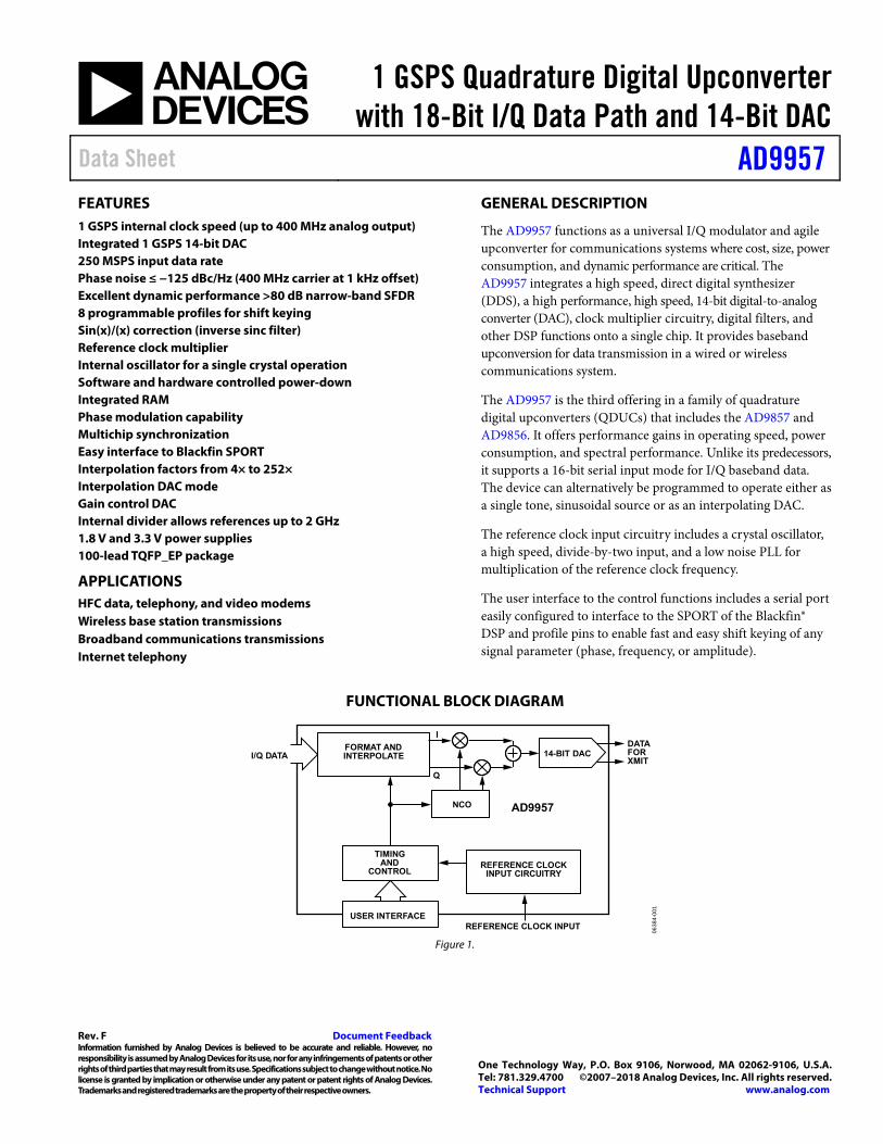
1 GSPS Quadrature Digital Upconverter with 18-Bit I/Q Data Path and 14-Bit DAC Data Sheet AD9957 Rev. F Document Feedback Information furnished by Analog Devices is believed to be accurate and reliable. However, no responsibility is assumed by Analog Devices for its use, nor for any infringements of patents or other rights of third parties that may result from its use. Specifications subject to change without notice. No license is granted by implication or otherwise under any patent or patent rights of Analog Devices. Trademarks and registered trademarks are the property of their respective owners. One Technology Way, P.O. Box 9106, Norwood, MA 02062-9106, U.S.A. Tel: 781.329.4700 ©2007–2018 Analog Devices, Inc. All rights reserved. Technical Support www.analog.com FEATURES 1 GSPS internal clock speed (up to 400 MHz analog output) Integrated 1 GSPS 14-bit DAC 250 MSPS input data rate Phase noise ≤ −125 dBc/Hz (400 MHz carrier at 1 kHz offset) Excellent dynamic performance >80 dB narrow-band SFDR 8 programmable profiles for shift keying Sin(x)/(x) correction (inverse sinc filter) Reference clock multiplier Internal oscillator for a single crystal operation Software and hardware controlled power-down Integrated RAM Phase modulation capability Multichip synchronization Easy interface to Blackfin SPORT Interpolation factors from 4× to 252× Interpolation DAC mode Gain control DAC Internal divider allows references up to 2 GHz 1.8 V and 3.3 V power supplies 100-lead TQFP_EP package APPLICATIONS HFC data, telephony, and video modems Wireless base station transmissions Broadband communications transmissions Internet telephony GENERAL DESCRIPTION The AD9957 functions as a universal I/Q modulator and agile upconverter for communications systems where cost, size, power consumption, and dynamic performance are critical. The AD9957 integrates a high speed, direct digital synthesizer (DDS), a high performance, high speed, 14-bit digital-to-analog converter (DAC), clock multiplier circuitry, digital filters, and other DSP functions onto a single chip. It provides baseband upconversion for data transmission in a wired or wireless communications system. The AD9957 is the third offering in a family of quadrature digital upconverters (QDUCs) that includes the AD9857 and AD9856. It offers performance gains in operating speed, power consumption, and spectral performance. Unlike its predecessors, it supports a 16-bit serial input mode for I/Q baseband data. The device can alternatively be programmed to operate either as a single tone, sinusoidal source or as an interpolating DAC. The reference clock input circuitry includes a crystal oscillator, a high speed, divide-by-two input, and a low noise PLL for multiplication of the reference clock frequency. The user interface to the control functions includes a serial port easily configured to interface to the SPORT of the Blackfin® DSP and profile pins to enable fast and easy shift keying of any signal parameter (phase, frequency, or amplitude). FUNCTIONAL BLOCK DIAGRAM FORMAT AND INTERPOLATE NCO I Q REFERENCE CLOCK INPUT I/Q DATA DATA FOR XMIT REFERENCE CLOCK INPUT CIRCUITRY TIMING AND CONTROL 14-BIT DAC USER INTERFACE 06384-001 AD9957 Figure 1.
Transcript of 1 GSPS Quadrature Digital Upconverter with 18-Bit I/Q · PDF file · 2018-01-271...
1 GSPS Quadrature Digital Upconverter with 18-Bit I/Q Data Path and 14-Bit DAC
Data Sheet AD9957
Rev. F Document Feedback Information furnished by Analog Devices is believed to be accurate and reliable. However, no responsibility is assumed by Analog Devices for its use, nor for any infringements of patents or other rights of third parties that may result from its use. Specifications subject to change without notice. No license is granted by implication or otherwise under any patent or patent rights of Analog Devices. Trademarks and registered trademarks are the property of their respective owners.
One Technology Way, P.O. Box 9106, Norwood, MA 02062-9106, U.S.A.Tel: 781.329.4700 ©2007–2018 Analog Devices, Inc. All rights reserved. Technical Support www.analog.com
FEATURES 1 GSPS internal clock speed (up to 400 MHz analog output) Integrated 1 GSPS 14-bit DAC 250 MSPS input data rate Phase noise ≤ −125 dBc/Hz (400 MHz carrier at 1 kHz offset) Excellent dynamic performance >80 dB narrow-band SFDR 8 programmable profiles for shift keying Sin(x)/(x) correction (inverse sinc filter) Reference clock multiplier Internal oscillator for a single crystal operation Software and hardware controlled power-down Integrated RAM Phase modulation capability Multichip synchronization Easy interface to Blackfin SPORT Interpolation factors from 4× to 252× Interpolation DAC mode Gain control DAC Internal divider allows references up to 2 GHz 1.8 V and 3.3 V power supplies 100-lead TQFP_EP package
APPLICATIONS HFC data, telephony, and video modems Wireless base station transmissions Broadband communications transmissions Internet telephony
GENERAL DESCRIPTION
The AD9957 functions as a universal I/Q modulator and agile upconverter for communications systems where cost, size, power consumption, and dynamic performance are critical. The AD9957 integrates a high speed, direct digital synthesizer (DDS), a high performance, high speed, 14-bit digital-to-analog converter (DAC), clock multiplier circuitry, digital filters, and other DSP functions onto a single chip. It provides baseband upconversion for data transmission in a wired or wireless communications system.
The AD9957 is the third offering in a family of quadrature digital upconverters (QDUCs) that includes the AD9857 and AD9856. It offers performance gains in operating speed, power consumption, and spectral performance. Unlike its predecessors, it supports a 16-bit serial input mode for I/Q baseband data. The device can alternatively be programmed to operate either as a single tone, sinusoidal source or as an interpolating DAC.
The reference clock input circuitry includes a crystal oscillator, a high speed, divide-by-two input, and a low noise PLL for multiplication of the reference clock frequency.
The user interface to the control functions includes a serial port easily configured to interface to the SPORT of the Blackfin® DSP and profile pins to enable fast and easy shift keying of any signal parameter (phase, frequency, or amplitude).
FUNCTIONAL BLOCK DIAGRAM
FORMAT ANDINTERPOLATE
NCO
I
Q
REFERENCE CLOCK INPUT
I/Q DATADATAFORXMIT
REFERENCE CLOCKINPUT CIRCUITRY
TIMINGAND
CONTROL
14-BIT DAC
USER INTERFACE
0638
4-00
1
AD9957
Figure 1.
AD9957 Data Sheet
Rev. F | Page 2 of 61
TABLE OF CONTENTS Features .............................................................................................. 1
Applications ....................................................................................... 1
General Description ......................................................................... 1
Functional Block Diagram .............................................................. 1
Revision History ............................................................................... 4
Specifications ..................................................................................... 5
Electrical Specifications ............................................................... 5
Absolute Maximum Ratings ............................................................ 8
ESD Caution .................................................................................. 8
Pin Configuration and Function Descriptions ............................. 9
Typical Performance Characteristics ........................................... 12
Modes of Operation ....................................................................... 16
Overview ...................................................................................... 16
Quadrature Modulation Mode ................................................. 17
BlackFin Interface (BFI) Mode ................................................. 18
Interpolating DAC Mode .......................................................... 19
Single Tone Mode ....................................................................... 20
Signal Processing ............................................................................ 21
Parallel Data Clock (PDCLK) ................................................... 21
Transmit Enable Pin (TxENABLE) .......................................... 21
Input Data Assembler ................................................................ 22
Inverse CCI Filter ....................................................................... 23
Fixed Interpolator (4×) .............................................................. 23
Programmable Interpolating Filter .......................................... 24
QDUC Mode ........................................................................... 24
BFI Mode ................................................................................. 24
Quadrature Modulator .............................................................. 25
DDS Core ..................................................................................... 25
Inverse Sinc Filter ....................................................................... 25
Output Scale Factor (OSF) ........................................................ 26
14-Bit DAC .................................................................................. 26
Auxiliary DAC ........................................................................ 26
RAM Control .................................................................................. 27
RAM Overview ........................................................................... 27
RAM Segment Registers ............................................................ 27
RAM State Machine ................................................................... 27
RAM Trigger (RT) Pin ............................................................... 27
Load/Retrieve RAM Operation ................................................ 28
RAM Playback Operation ......................................................... 28
Overview of RAM Playback Modes ......................................... 29
RAM Ramp-Up Mode ........................................................... 29
RAM Bidirectional Ramp Mode .......................................... 30
RAM Continuous Bidirectional Ramp Mode .................... 32
RAM Continuous Recirculate Mode ................................... 33
Clock Input (REF_CLK) ................................................................ 34
REFCLK Overview ..................................................................... 34
Crystal Driven REF_CLK ......................................................... 34
Direct Driven REF_CLK ........................................................... 34
Phase-Locked Loop (PLL) Multiplier ...................................... 35
PLL Charge Pump ...................................................................... 36
External PLL Loop Filter Components ................................... 36
PLL Lock Indication .................................................................. 36
Additional Features ........................................................................ 37
Output Shift Keying (OSK) ....................................................... 37
Manual OSK ............................................................................ 37
Automatic OSK ....................................................................... 37
Profiles ......................................................................................... 38
I/O_UPDATE Pin ...................................................................... 38
Automatic I/O Update ............................................................... 38
Power-Down Control ................................................................ 39
General-Purpose I/O (GPIO) Port .......................................... 39
Synchronization of Multiple Devices ........................................... 40
Overview ..................................................................................... 40
Clock Generator ......................................................................... 40
Data Sheet AD9957
Rev. F | Page 3 of 61
Sync Generator ............................................................................ 41
Sync Receiver ............................................................................... 41
Setup/Hold Validation ................................................................ 42
Synchronization Example .......................................................... 44
I/Q Path Latency ......................................................................... 45
Example .................................................................................... 45
Power Supply Partitioning ............................................................. 46
3.3 V Supplies .............................................................................. 46
DVDD_I/O (Pin 11, Pin 15, Pin 21, Pin 28, Pin 45, Pin 56, Pin 66) ...................................................................................... 46
AVDD (Pin 74 to Pin 77 and Pin 83) ................................... 46
1.8 V Supplies .............................................................................. 46
DVDD (Pin 17, Pin 23, Pin 30, Pin 47, Pin 57, Pin 64) ..... 46
AVDD (Pin 3) .......................................................................... 46
AVDD (Pin 6) .......................................................................... 46
AVDD (Pin 89 and Pin 92) .................................................... 46
Serial Programming ........................................................................ 47
Control Interface—Serial I/O .................................................... 47
General Serial I/O Operation .................................................... 47
Instruction Byte ........................................................................... 47
Instruction Byte Information Bit Map ................................. 47
Serial I/O Port Pin Descriptions ............................................... 47
SCLK—Serial Clock................................................................ 47
CS—Chip Select Bar ............................................................... 47
SDIO—Serial Data Input/Output ......................................... 47
SDO—Serial Data Out ........................................................... 48
I/O_RESET—Input/Output Reset ........................................ 48
I/O_UPDATE—Input/Output Update ................................ 48
Serial I/O Timing Diagrams ...................................................... 48
MSB/LSB Transfers ..................................................................... 48
I/O_UPDATE, SYNC_CLK, and System Clock Relationships ....................................................................................................... 49
Register Map and Bit Descriptions ............................................... 50
Register Map ................................................................................ 50
Register Bit Descriptions............................................................ 55
Control Function Register 1 (CFR1) .................................... 55
Control Function Register 2 (CFR2) .................................... 56
Control Function Register 3 (CFR3) .................................... 58
Auxiliary DAC Control Register ........................................... 58
I/O Update Rate Register ....................................................... 58
RAM Segment Register 0 ....................................................... 58
RAM Segment Register 1 ....................................................... 59
Amplitude Scale Factor (ASF) Register ............................... 59
Multichip Sync Register ......................................................... 59
Profile Registers ........................................................................... 60
Profile[7:0] Register—Single Tone ....................................... 60
Profile[7:0] Register—QDUC ............................................... 60
RAM Register .......................................................................... 60
GPIO Configuration Register ............................................... 60
GPIO Data Register ................................................................ 60
Outline Dimensions ........................................................................ 61
Ordering Guide ........................................................................... 61

AD9957 Data Sheet
Rev. F | Page 4 of 61
REVISION HISTORY 4/2018—Rev. E to Rev. F Moved Sync Generator Section .................................................... 41 Changes to Sync Generator Section, Figure 56, and Sync Receiver Section .............................................................................. 41 5/2017—Rev. D to Rev. E Changes to External PLL Loop Filter Components Section ..... 36 1/2016—Rev. C to Rev. D Changes to Table 3 .......................................................................... 11 Changes to Figure 27 ...................................................................... 18 4/2012—Rev. B to Rev. C Changes to Table 1 ............................................................................ 7 Changes to Table 3 .......................................................................... 11 Change to Sync Generator Section ............................................... 41 Changes to Sync Receiver Section and Setup/Hold Validation Section .............................................................................................. 42 Changes to Table 13 ........................................................................ 50 Changes to Table 19 ........................................................................ 57 Changes to Table 26 ........................................................................ 59 10/2010—Rev. A to Rev. B Changes to Data Rate in Features Section ..................................... 1 Changes to Specifications Section .................................................. 6 Added EPAD Notation to Figure 4 and Table 3 ........................... 9 Changes to XTAL_SEL Pin Description ...................................... 11 Changes to BlackFin Interface (BFI) Mode Section .................. 18 Changes to Figure 30 and Figure 31 ............................................. 22 Changes to Programmable Interpolating Filter Section ............ 24 Changes to Fifth Paragraph of Quadrature Modulator Section...... 25 Changes to RAM Segment Registers Section ............................. 27 Changes to RAM Playback Operation Section ........................... 28 Changes to Control Interface—Serial I/O Section ..................... 47 Added to I/O_UPDATE, SYNC_CLK, and System Clock Relationships Section and Figure 64 ............................................ 49 Changes to Default Values of Profile 0 Register—Single Tone (0x0E) and Profile 0 Register—QDUC (0x0E) in Table 14 ....... 51 Changes to Default Values in Table 15 ......................................... 52 Changes to Default Values in Table 16 ......................................... 53 Changes to Default Values in Table 17 ......................................... 54 Updated Outline Dimensions ....................................................... 61
1/2008—Rev. 0 to Rev. A Changes to REFCLK Multiplier Specification ............................... 3 Changes to I/O_UPDATE/Profile<2:0>/RT Timing Characteristics and I/Q Input Timing Characteristics ................. 5 Replaced Pin Configuration and Function Descriptions Section ................................................................................................. 8 Changes to Figure 25 Through Figure 29.................................... 15 Deleted Table 4, Renumbered Sequentially ................................ 20 Changes to DDS Core Section ...................................................... 24 Changes to Figure 47 and Table 6................................................. 33 Replaced Synchronization of Multiple Devices Section ............ 39 Added I/Q Path Latency Section .................................................. 44 Added Power Supply Partitioning Section .................................. 45 Changes to General Serial I/O Operation Section ..................... 46 Changes to Table 13 ....................................................................... 48 Changes to Table 14 ....................................................................... 49 Changes to Table 19 ....................................................................... 54 Changes to Table 20 ....................................................................... 56 Changes to GPIO Configuration Register and GPIO Data Register Sections ........................................................ 58 5/2007—Revision 0: Initial Version

Data Sheet AD9957
Rev. F | Page 5 of 61
SPECIFICATIONS ELECTRICAL SPECIFICATIONS AVDD (1.8V) and DVDD (1.8V) = 1.8 V ± 5%, AVDD (3.3V) = 3.3 V ± 5%, DVDD_I/O (3.3V) = 3.3 V ± 5%, T = 25°C, RSET = 10 kΩ, IOUT = 20 mA, external reference clock frequency = 1000 MHz with REFCLK multiplier disabled, unless otherwise noted.
Table 1. Parameter Test Conditions/Comments Min Typ Max Unit REF_CLK INPUT CHARACTERISTICS
Frequency Range REFCLK Multiplier Disabled 60 10001 MHz Enabled 3.2 60 MHz Maximum REFCLK Input Divider Frequency Full temperature range 1500 1900 MHz Minimum REFCLK Input Divider Frequency Full temperature range 25 35 MHz
External Crystal 25 MHz Input Capacitance 3 pF Input Impedance (Differential) 2.8 kΩ Input Impedance (Single-Ended) 1.4 kΩ Duty Cycle REFCLK multiplier disabled 45 55 % REFCLK multiplier enabled 40 60 % REF_CLK Input Level Single-ended 50 1000 mV p-p Differential 100 2000 mV p-p
REFCLK MULTIPLIER VCO GAIN CHARACTERISTICS VCO Gain (KV) at Center Frequency VCO0 range setting 429 MHz/V
VCO1 range setting 500 MHz/V VCO2 range setting 555 MHz/V VCO3 range setting 750 MHz/V VCO4 range setting 789 MHz/V VCO5 range setting2 850 MHz/V REFCLK_OUT CHARACTERISTICS
Maximum Capacitive Load 20 pF Maximum Frequency 25 MHz
DAC OUTPUT CHARACTERISTICS Full-Scale Output Current 8.6 20 31.6 mA Gain Error −10 +10 %FS Output Offset 2.3 µA Differential Nonlinearity 0.8 LSB Integral Nonlinearity 1.5 LSB Output Capacitance 5 pF Residual Phase Noise At 1 kHz offset, 20 MHz AOUT
REFCLK Multiplier Disabled −152 dBc/Hz Enabled at 20× −140 dBc/Hz Enabled at 100× −140 dBc/Hz
AC Voltage Compliance Range −0.5 +0.5 V SPURIOUS-FREE DYNAMIC RANGE (SFDR SINGLE TONE)
fOUT = 20.1 MHz −70 dBc fOUT = 98.6 MHz −69 dBc fOUT = 201.1 MHz −61 dBc fOUT = 397.8 MHz −54 dBc
AD9957 Data Sheet
Rev. F | Page 6 of 61
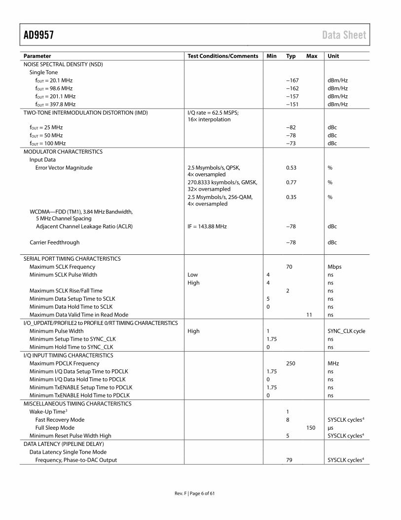
Parameter Test Conditions/Comments Min Typ Max Unit NOISE SPECTRAL DENSITY (NSD)
Single Tone fOUT = 20.1 MHz −167 dBm/Hz fOUT = 98.6 MHz −162 dBm/Hz fOUT = 201.1 MHz −157 dBm/Hz fOUT = 397.8 MHz −151 dBm/Hz
TWO-TONE INTERMODULATION DISTORTION (IMD) I/Q rate = 62.5 MSPS; 16× interpolation
fOUT = 25 MHz −82 dBc fOUT = 50 MHz −78 dBc fOUT = 100 MHz −73 dBc
MODULATOR CHARACTERISTICS Input Data
Error Vector Magnitude 2.5 Msymbols/s, QPSK, 4× oversampled
0.53 %
270.8333 ksymbols/s, GMSK, 32× oversampled
0.77 %
2.5 Msymbols/s, 256-QAM, 4× oversampled
0.35 %
WCDMA—FDD (TM1), 3.84 MHz Bandwidth, 5 MHz Channel Spacing
Adjacent Channel Leakage Ratio (ACLR) IF = 143.88 MHz −78 dBc Carrier Feedthrough −78 dBc
SERIAL PORT TIMING CHARACTERISTICS
Maximum SCLK Frequency 70 Mbps Minimum SCLK Pulse Width Low 4 ns High 4 ns Maximum SCLK Rise/Fall Time 2 ns Minimum Data Setup Time to SCLK 5 ns Minimum Data Hold Time to SCLK 0 ns Maximum Data Valid Time in Read Mode 11 ns
I/O_UPDATE/PROFILE2 to PROFILE 0/RT TIMING CHARACTERISTICS Minimum Pulse Width High 1 SYNC_CLK cycle Minimum Setup Time to SYNC_CLK 1.75 ns Minimum Hold Time to SYNC_CLK 0 ns
I/Q INPUT TIMING CHARACTERISTICS Maximum PDCLK Frequency 250 MHz Minimum I/Q Data Setup Time to PDCLK 1.75 ns Minimum I/Q Data Hold Time to PDCLK 0 ns Minimum TxENABLE Setup Time to PDCLK 1.75 ns Minimum TxENABLE Hold Time to PDCLK 0 ns
MISCELLANEOUS TIMING CHARACTERISTICS Wake-Up Time3 1
Fast Recovery Mode 8 SYSCLK cycles4 Full Sleep Mode 150 μs
Minimum Reset Pulse Width High 5 SYSCLK cycles4 DATA LATENCY (PIPELINE DELAY)
Data Latency Single Tone Mode Frequency, Phase-to-DAC Output 79 SYSCLK cycles4

Data Sheet AD9957
Rev. F | Page 7 of 61
Parameter Test Conditions/Comments Min Typ Max Unit CMOS LOGIC INPUTS
Voltage Logic 1 2.0 V Logic 0 0.8 V
Current Logic 1 90 150 µA Logic 0 90 150 µA
Input Capacitance 2 pF XTAL_SEL INPUT
Logic 1 Voltage 1.25 V Logic 0 Voltage 0.6 V Input Capacitance 2 pF
CMOS LOGIC OUTPUTS 1 mA load Voltage
Logic 1 2.8 V Logic 0 0.4 V
POWER SUPPLY CURRENT DVDD_I/O (3.3V) Pin Current Consumption QDUC mode 16 mA DVDD (1.8V) Pin Current Consumption QDUC mode 610 mA AVDD (3.3V) Pin Current Consumption QDUC mode 28 mA AVDD (1.8V) Pin Current Consumption QDUC mode 105 mA
POWER CONSUMPTION Single Tone Mode 800 mW Continuous Modulation 8× interpolation 1400 1800 mW Inverse Sinc Filter Power Consumption 150 200 mW Full Sleep Mode 12 40 mW
1 The system clock is limited to 750 MHz maximum in BFI mode. 2 The gain value for VCO range Setting 5 is measured at 1000 MHz. 3 Wake-up time refers to the recovery from analog power-down modes. The longest time required is for the Reference Clock Multiplier PLL to relock to the reference. 4 SYSCLK cycle refers to the actual clock frequency used on-chip by the DDS. If the reference clock multiplier is used to multiply the external reference clock frequency,
the SYSCLK frequency is the external frequency multiplied by the reference clock multiplication factor. If the reference clock multiplier and divider are not used, the SYSCLK frequency is the same as the external reference clock frequency.
AD9957 Data Sheet
Rev. F | Page 8 of 61
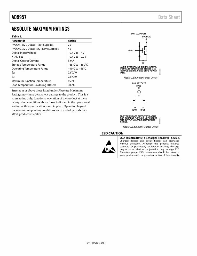
ABSOLUTE MAXIMUM RATINGS Table 2. Parameter Rating AVDD (1.8V), DVDD (1.8V) Supplies 2 V AVDD (3.3V), DVDD_I/O (3.3V) Supplies 4 V Digital Input Voltage −0.7 V to +4 V XTAL_SEL −0.7 V to +2.2 V Digital Output Current 5 mA Storage Temperature Range −65°C to +150°C Operating Temperature Range −40°C to +85°C θJA 22°C/W
θJC 2.8°C/W
Maximum Junction Temperature 150°C Lead Temperature, Soldering (10 sec) 300°C
Stresses at or above those listed under Absolute Maximum Ratings may cause permanent damage to the product. This is a stress rating only; functional operation of the product at these or any other conditions above those indicated in the operational section of this specification is not implied. Operation beyond the maximum operating conditions for extended periods may affect product reliability.
0638
4-00
3
AVOID OVERDRIVING DIGITAL INPUTS.FORWARD BIASING ESD DIODES MAYCOUPLE DIGITAL NOISE ONTO POWERPINS.
DIGITAL INPUTS
INPUT
DVDD_I/O
Figure 2. Equivalent Input Circuit
0638
4-05
5
MUST TERMINATE OUTPUTS TO AGNDFOR CURRENT FLOW. DO NOT EXCEEDTHE OUTPUT VOLTAGE COMPLIANCERATING.
IOUT IOUT
DAC OUTPUTSAVDD
Figure 3. Equivalent Output Circuit
ESD CAUTION
Data Sheet AD9957
Rev. F | Page 9 of 61
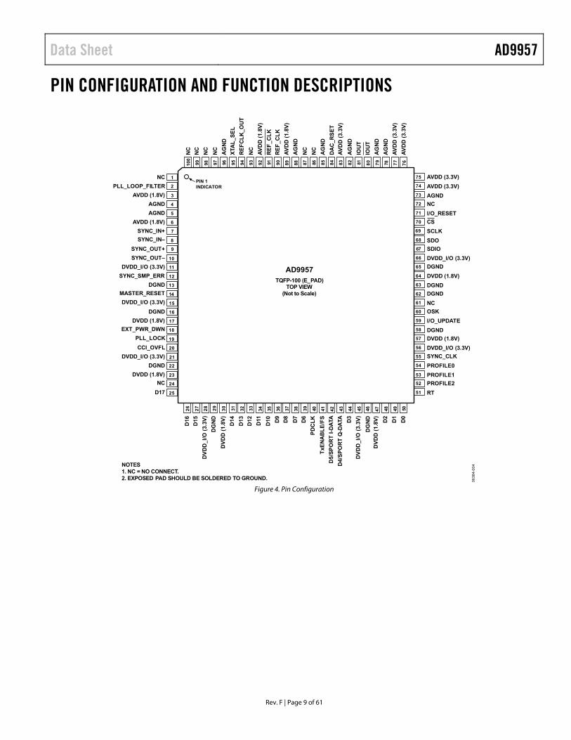
PIN CONFIGURATION AND FUNCTION DESCRIPTIONS
26
27
28 29
30
55
54
53
52
51
TQFP-100 (E_PAD)TOP VIEW
(Not to Scale)
AD9957
D16
D15
DV
DD
_I/O
(3.
3V)
DG
ND
DV
DD
(1.
8V)
5
4
3
2
7
6
9
8
1
11
10
16
15
14
13
18
17
20
19
22
21
12
24
23
25
32 33 34 35 36 38 39 40 41 42 43 44 45 46 47 48 49 5031 37
D14
D13
D12
D11
D10 D
9
D8
D7
D6
PD
CL
K
TxE
NA
BL
E/F
S
DG
ND
D5/
SP
OR
T I
-DA
TA
D4/
SP
OR
T Q
-DA
TA D3
DV
DD
_I/O
(3.
3V)
DV
DD
(1.
8V)
D2
D1
D0
80
IOU
T
79
AG
ND
78A
GN
D
77
AV
DD
(3.
3V)
76
AV
DD
(3.
3V)
75 AVDD (3.3V)
74 AVDD (3.3V)
73 AGND
72 NC
71 I/O_RESET
70 CS
69 SCLK
68 SDO
67 SDIO
66 DVDD_I/O (3.3V)
65 DGND
64 DVDD (1.8V)
63 DGND
62 DGND
61 NC
60 OSK
59 I/O_UPDATE
58 DGND
57 DVDD (1.8V)
56 DVDD_I/O (3.3V)
SYNC_CLK
PROFILE0
PROFILE1
PROFILE2
RT
100
99 98 97 96 95 94 93 92 91 90 89 88 87 86 85 84 83 82 81
NC
NC
NC
NC
AG
ND
XTA
L_S
EL
RE
FC
LK
_OU
T
NC
AV
DD
(1.
8V)
RE
F_C
LK
RE
F_C
LK
AV
DD
(1.
8V)
AG
ND
NC
NC
AG
ND
DA
C_R
SE
T
AV
DD
(3.
3V)
AG
ND
IOU
T
NC
PLL_LOOP_FILTER
AVDD (1.8V)
AGND
AGND
AVDD (1.8V)
SYNC_IN+
SYNC_IN–
SYNC_OUT+
SYNC_OUT–
DVDD_I/O (3.3V)
SYNC_SMP_ERR
DGND
MASTER_RESET
DVDD_I/O (3.3V)
DGND
DVDD (1.8V)
EXT_PWR_DWN
PLL_LOCK
CCI_OVFL
DVDD_I/O (3.3V)
DGND
DVDD (1.8V)
NC
D17
0638
4-00
4
PIN 1INDICATOR
NOTES1. NC = NO CONNECT.2. EXPOSED PAD SHOULD BE SOLDERED TO GROUND.
Figure 4. Pin Configuration
AD9957 Data Sheet
Rev. F | Page 10 of 61
Table 3. Pin Function Descriptions Pin No. Mnemonic I/O1 Description 1, 24, 61, 72, 86, 87, 93,
97 to 100 NC Not Connected. Allow the device pin to float.
2 PLL_LOOP_FILTER I PLL Loop Filter Compensation. See External PLL Loop Filter Components section. 3, 6, 89, 92 AVDD (1.8V) I Analog Core VDD. 1.8 V analog supplies. 74 to 77, 83 AVDD (3.3V) I Analog DAC VDD. 3.3 V analog supplies. 17, 23, 30, 47, 57, 64 DVDD (1.8V) I Digital Core VDD. 1.8 V digital supplies. 11, 15, 21, 28, 45, 56, 66 DVDD_I/O (3.3V) I Digital Input/Output VDD. 3.3 V digital supplies. 4, 5, 73, 78, 79, 82, 85,
88, 96 AGND I Analog Ground.
13, 16, 22, 29, 46, 58, 62, 63, 65
DGND I Digital Ground.
7 SYNC_IN+ I Synchronization Signal, Digital Input (Rising Edge Active). Synchronization signal from external master to synchronize internal subclocks. See the Synchronization of Multiple Devices section.
8 SYNC_IN− I Synchronization Signal, Digital Input (Falling Edge Active). Synchronization signal from external master to synchronize internal subclocks. See the Synchronization of Multiple Devices section.
9 SYNC_OUT+ O Synchronization Signal, Digital Output (Rising Edge Active). Synchronization signal from internal device subclocks to synchronize external slave devices. See the Synchronization of Multiple Devices section.
10 SYNC_OUT− O Synchronization Signal, Digital Output (Falling Edge Active). Synchronization signal from internal device subclocks to synchronize external slave devices. See the Synchronization of Multiple Devices section.
12 SYNC_SMP_ERR O Synchronization Sample Error, Digital Output (Active High). A high on this pin indicates that the AD9957 did not receive a valid sync signal on SYNC_IN+/SYNC_IN−. See the Synchronization of Multiple Devices section.
14 MASTER_RESET I Master Reset, Digital Input (Active High). This pin clears all memory elements and sets registers to default values.
18 EXT_PWR_DWN I External Power-Down, Digital Input (Active High). A high level on this pin initiates the currently programmed power-down mode. See the Power-Down Control section for further details. If unused, tie to ground.
19 PLL_LOCK O PLL Lock, Digital Output (Active High). A high on this pin indicates that the clock multiplier PLL has acquired lock to the reference clock input.
20 CCI_OVFL O CCI Overflow Digital Output, Active High. A high on this pin indicates a CCI filter overflow. This pin remains high until the CCI overflow condition is cleared.
25 to 27, 31 to 39, 42 to 44, 48 to 50
D[17:0] I/O Parallel Data Input Bus (Active High). These pins provide the interleaved, 18-bit, digital, I and Q vectors for the modulator to upconvert. Also used for a GPIO port in Blackfin interface mode.
42 SPORT I-DATA I I-Data Serial Input. In Blackfin interface mode, this pin serves as the I-data serial input. 43 SPORT Q-DATA I Q-Data Serial Input. In Blackfin interface mode, this pin serves as the Q-data serial
input. 40 PDCLK O Parallel Data Clock, Digital Output (Clock). See the Signal Processing section for details. 41 TxENABLE/FS I Transmit Enable, Digital Input (Active High). See the Signal Processing section for
details. In Blackfin interface mode, this pin serves as the FS input to receive the RFS output signal from the Blackfin.
51 RT I RAM Trigger, Digital Input (Active High). This pin provides control for the RAM amplitude scaling function. When this function is engaged, a high sweeps the amplitude from the beginning RAM address to the end. A low sweeps the amplitude from the end RAM address to the beginning. If unused, connect to ground or supply.
52 to 54 PROFILE2, PROFILE1, PROFILE0
I Profile Select Pins, Digital Inputs (Active High). These pins select one of eight phase/frequency profiles for the DDS core (single tone or carrier tone). Changing the state of one of these pins transfers the current contents of all I/O buffers to the corresponding registers. Set up state changes to the SYNC_CLK pin.
55 SYNC_CLK O Output System Clock/4, Digital Output (Clock). Set up the I/O_UPDATE and PROFILE2/PROFILE1/PROFILE0 pins to the rising edge of this signal.

Data Sheet AD9957
Rev. F | Page 11 of 61
Pin No. Mnemonic I/O1 Description 59 I/O_UPDATE I/O Input/Output Update; Digital Input Or Output (Active High), Depending on the
Internal I/O Update Active Bit. A high on this pin indicates a transfer of the contents of the I/O buffers to the corresponding internal registers.
60 OSK I Output Shift Keying, Digital Input (Active High). When using OSK (manual or automatic), this pin controls the OSK function. See the Output Shift Keying (OSK) section of the data sheet for details. When not using OSK, tie this pin high.
67 SDIO I/O Serial Data Input/Output, Digital Input/Output (Active High). This pin can be either unidirectional or bidirectional (default), depending on configuration settings. In bidirectional serial port mode, this pin acts as the serial data input and output. In unidirectional, it is an input only.
68 SDO O Serial Data Output, Digital Output (Active High). This pin is only active in unidirectional serial data mode. In this mode, it functions as the output. In bidirectional mode, this pin is not operational and must be left floating.
69 SCLK I Serial Data Clock. Digital clock (rising edge on write, falling edge on read). This pin provides the serial data clock for the control data path. Write operations to the AD9957 use the rising edge. Readback operations from the AD9957 use the falling edge.
70 CS I Chip Select, Digital Input (Active Low). Bringing this pin low enables the AD9957 to detect serial clock rising/falling edges. Bringing this pin high causes the AD9957 to ignore input on the serial data pins.
71 I/O_RESET I Input/Output Reset. Digital input (active high). This pin can be used when a serial I/O communication cycle fails (see the I/O_RESET—Input/Output Reset section for details). When not used, connect this pin to ground.
80 IOUT O Open-Source DAC Complementary Output Source. Analog output, current mode. Connect through 50 Ω to AGND.
81 IOUT O Open-Source DAC Output Source. Analog output, current mode. Connect through 50 Ω to AGND.
84 DAC_RSET O Analog Reference Pin. This pin programs the DAC output full-scale reference current. Attach a 10 kΩ resistor to AGND.
90 REF_CLK I Reference Clock Input. Analog input. See the REFCLK Overview section for more details.
91 REF_CLK I Complementary Reference Clock Input. Analog input. See the REFCLK Overview section for more details.
94 REFCLK_OUT O Reference Clock Output. Analog output. See the REFCLK Overview section for more details. 95 XTAL_SEL I Crystal Select (1.8 V Logic). Analog input (active high). Driving the XTAL_SEL pin high
enables the internal oscillator to be used with a crystal resonator. If unused, connect it to AGND.
EPAD Exposed Pad (EPAD). The exposed pad should be soldered to ground. 1 I is input, O is output, and I/O is for input/output.

AD9957 Data Sheet
Rev. F | Page 12 of 61
TYPICAL PERFORMANCE CHARACTERISTICS 0
–20
–10
–50
–40
–30
–80
–70
–60
–90
–100START 0Hz 50MHz/DIV STOP 500MHz
0638
4-04
8
1
1
Figure 5. 15.625 kHz Quadrature Tone, Carrier = 102 MHz, CCI = 16, fS = 1 GHz
0
–20
–10
–50
–40
–30
–80
–70
–60
–90
–100START 0MHz 50MHz/DIV STOP 500MHz
0638
4-05
0
1
1
Figure 6. 15.625 kHz Quadrature Tone, Carrier = 222 MHz,
CCI = 16, fS = 1 GHz
0
–20
–10
–50
–40
–30
–80
–70
–60
–90
–100START 0Hz 50MHz/DIV STOP 500MHz
0638
4-05
2
1
1
Figure 7. 15.625 kHz Quadrature Tone, Carrier = 372 MHz,
CCI = 16, fS = 1 GHz
0
–20
–10
–50
–40
–30
–80
–70
–60
–90
–100CENTER 102MHz 5kHz/DIV SPAN 50kHz
0638
4-04
9
1
1
Figure 8. Narrow-Band View of Figure 5
(with Carrier and Lower Sideband Suppression)
0
–20
–10
–50
–40
–30
–80
–70
–60
–90
–100CENTER 222MHz 5kHz/DIV SPAN 50kHz
0638
4-05
1
1
1
Figure 9. Narrow-Band View of Figure 6 (with Carrier And Lower Sideband Suppression)
0
–20
–10
–50
–40
–30
–80
–70
–60
–90
–100CENTER 372MHz 5kHz/DIV SPAN 50kHz
0638
4-05
3
1
1
Figure 10. Narrow-Band View of Figure 7
(with Carrier and Lower Sideband Suppression)
Data Sheet AD9957
Rev. F | Page 13 of 61
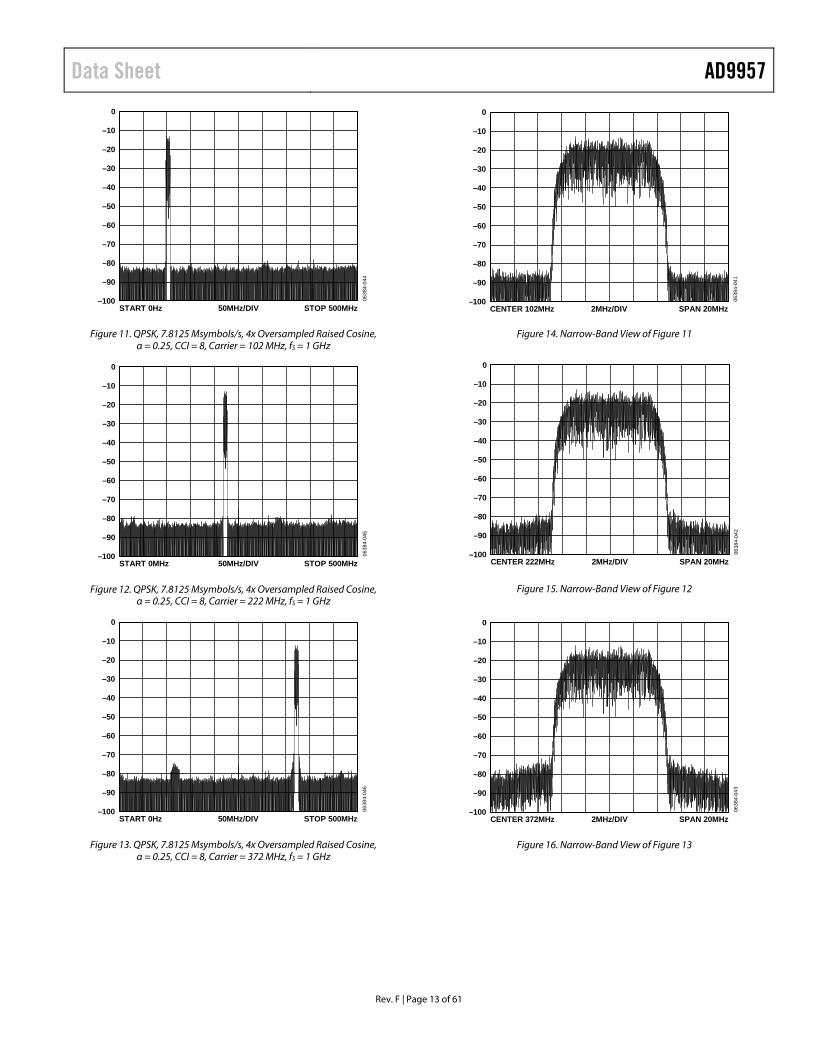
0
–20
–10
–50
–40
–30
–80
–70
–60
–90
–100START 0Hz 50MHz/DIV STOP 500MHz
0638
4-04
4
Figure 11. QPSK, 7.8125 Msymbols/s, 4x Oversampled Raised Cosine, α = 0.25, CCI = 8, Carrier = 102 MHz, fS = 1 GHz
0
–20
–10
–50
–40
–30
–80
–70
–60
–90
–100START 0MHz 50MHz/DIV STOP 500MHz
0638
4-04
5
Figure 12. QPSK, 7.8125 Msymbols/s, 4x Oversampled Raised Cosine, α = 0.25, CCI = 8, Carrier = 222 MHz, fS = 1 GHz
0
–20
–10
–50
–40
–30
–80
–70
–60
–90
–100START 0Hz 50MHz/DIV STOP 500MHz
0638
4-04
6
Figure 13. QPSK, 7.8125 Msymbols/s, 4x Oversampled Raised Cosine, α = 0.25, CCI = 8, Carrier = 372 MHz, fS = 1 GHz
0
–20
–10
–50
–40
–30
–80
–70
–60
–90
–100CENTER 102MHz 2MHz/DIV SPAN 20MHz
0638
4-04
1
Figure 14. Narrow-Band View of Figure 11
0
–20
–10
–50
–40
–30
–80
–70
–60
–90
–100CENTER 222MHz 2MHz/DIV SPAN 20MHz
0638
4-04
2
Figure 15. Narrow-Band View of Figure 12
0
–20
–10
–50
–40
–30
–80
–70
–60
–90
–100CENTER 372MHz 2MHz/DIV SPAN 20MHz
0638
4-04
3
Figure 16. Narrow-Band View of Figure 13

AD9957 Data Sheet
Rev. F | Page 14 of 61
–50
–55
–60
–65
–75
–70
0638
4-05
8
SFD
R (d
Bc)
FREQUENCY OUT (MHz)
SFDR WITHOUT PLL
SFDR WITH PLL
0 50 100 150 200 250 300 350 400
Figure 17. Wideband SFDR vs. Output Frequency in Single Tone Mode,
PLL with REFCLK = 15.625 MHz × 64
400 450300250 350200150100500
0638
4-05
9
SFD
R (d
Bc)
FREQUENCY OUT (MHz)
–75
–70
–65
–60
–55
–45
–50
LOW SUPPLY
HIGH SUPPLY
Figure 18. SFDR vs. Output Frequency and Supply (±5%) in Single Tone Mode, REFCLK = 1 GHz
400 450300250 350200150100500
0638
4-06
0
SFD
R (d
Bc)
FREQUENCY OUT (MHz)
–75
–70
–65
–60
–55
–50
–40°C
+85°C
Figure 19. SFDR vs. Frequency and Temperature in Single Tone Mode,
REFCLK = 1 GHz
–90
–100
–120
–110
–140
–150
–130
–170
–160
10 100 1k 10k 100k 100M1M 10M
0638
4-06
1
MA
GN
ITU
DE
(dB
c/H
z)
FREQUENCY OFFSET (Hz)
fOUT = 20.1MHz
fOUT = 98.6MHz
fOUT = 201.1MHz
fOUT = 397.8MHz
Figure 20. Residual Phase Noise, System Clock = 1 GHz
–90
–100
–110
–120
–130
–140
–150
–16010 100 1k 10k 100k 1M 10M 100M
0638
4-05
4
MA
GN
ITU
DE
(dB
c/ H
z)
FREQUENCY OFFSET (Hz)
fOUT = 20.1MHz
fOUT = 397.8MHz
fOUT = 98.6MHz
fOUT = 201.1MHz
Figure 21. Residual Phase Noise Using the REFCLK Multiplier,
REFCLK = 50 MHz with 20x Multiplication, System Clock = 1 GHz
1200
200
400
600
800
1000
0100 200 300 400 500 600 700 800 900 1000
0638
4-06
2
POW
ER D
ISSI
PATI
ON
(mW
)
SYSTEM CLOCK FREQUENCY (MHz)
DVDD 3.3VAVDD 3.3VAVDD 1.8V
DVDD 1.8V
Figure 22. Power Dissipation vs. System Clock (PLL Disabled)
Data Sheet AD9957
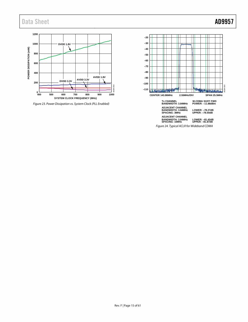
Rev. F | Page 15 of 61
1200
200
400
600
800
1000
0400 500 600 700 800 900 1000
0638
4-06
3
POW
ER D
ISSI
PATI
ON
(mW
)
SYSTEM CLOCK FREQUENCY (MHz)
DVDD 1.8V
AVDD 1.8VAVDD 3.3VDVDD 3.3V
Figure 23. Power Dissipation vs. System Clock (PLL Enabled)
0638
4-06
4
–110
–100
–90
–80
–70
–60
–50
–40
–30
–20
CENTER 143.86MHz SPAN 25.5MHz2.55MHz/DIV
Tx CHANNELBANDWIDTH: 3.84MHzADJACENT CHANNELBANDWIDTH: 3.84MHzSPACING: 3MHzADJACENT CHANNELBANDWIDTH: 3.84MHzSPACING: 10MHz
POWER: –11.88dBm
LOWER: –78.27dBUPPER: –78.50dB
LOWER: –81.42dBUPPER: –81.87dB
W-CDMA SGFF FWD
Figure 24. Typical ACLR for Wideband CDMA

AD9957 Data Sheet
Rev. F | Page 16 of 61
MODES OF OPERATION OVERVIEW The AD9957 has three basic operating modes.
• Quadrature modulation (QDUC) mode (default) • Interpolating DAC mode • Single tone mode
The active mode is selected via the operating mode bits in Control Function Register 1 (CFR1). Single tone mode allows the device to operate as a sinusoidal generator with the DDS driving the DAC directly.
Interpolating DAC mode bypasses the DDS, allowing the user to deliver baseband data to the device at a sample rate lower
than that of the DAC. An internal chain of rate interpolation filters the user data and upsamples to the DAC sample rate. Combined, the filters provide for programmable rate interpola-tion while suppressing spectral images and retaining the original baseband spectrum.
QDUC mode employs both the DDS and the rate interpolation filters. In this case, two parallel banks of rate interpolation filters allow baseband processing of in-phase and quadrature (I/Q) signals with the DDS providing the carrier signal to be modulated by the baseband signals. A detailed block diagram of the AD9957 is shown in Figure 25.
The inverse sinc filter is available in all three modes.
0638
4-00
5
PDCLK
I/Q IN
EXT_
PWR
_DW
N
DAC_RSET
IOUT
IOUT
TxENABLE
FTWPW
DAC GAIN
θ
INVE
RSE
SIN
CFI
LTER
CLOCKFTW
PW
8
SYSCLK
PLL
÷2
CLO
CK
MO
DE
REF_CLK
REF_CLK
REFCLK_OUT
XTAL_SEL
PARALLEL DATATIMING AND CONTROL
AD9957
ωcos (ωt+θ)
sin (ωt+θ)
SYN
C_O
UT
SYN
C_I
N
PLL_
LOC
K
PLL_
LOO
P_FI
LTER
MA
STER
_RES
ET
2 2
CC
I_O
VFL
OSK
DDSAUXDAC8-BIT
POWERDOWN
CONTROL
RT
RAM
PRO
FILE
SERIAL I/OPORT
I/O_U
PDA
TE
PROGRAMMINGREGISTERS
3I Q IS QS
18
DA
TA A
SSEM
BLE
R A
ND
FO
RM
ATT
ER
I
Q
IS
QS
BLA
CK
FIN
INTE
RFA
CE
18
18
16
16
HA
LF-B
AN
DFI
LTER
S (4
×)
INVE
RSE
CC
I
CC
I(1
× TO
63×
)
HA
LF-B
AN
DFI
LTER
S (4
×)
INVE
RSE
CC
I
CC
I(1
× TO
63×
)
OSK
INTERNAL CLOCK TIMING AND CONTROL
DAC14-BIT
OUTPUTSCALE
FACTOR
SDIO CS
I/O_R
ESET
SCLK
SDO
Figure 25. Detailed Block Diagram
Data Sheet AD9957
Rev. F | Page 17 of 61
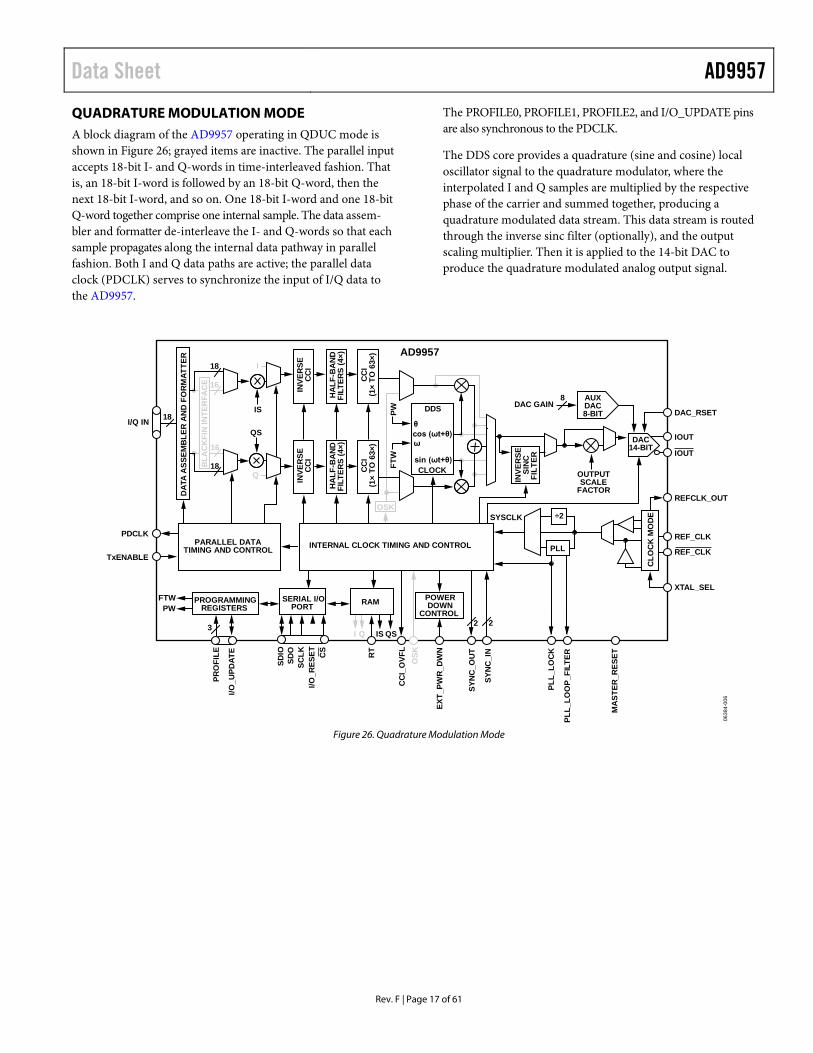
QUADRATURE MODULATION MODE A block diagram of the AD9957 operating in QDUC mode is shown in Figure 26; grayed items are inactive. The parallel input accepts 18-bit I- and Q-words in time-interleaved fashion. That is, an 18-bit I-word is followed by an 18-bit Q-word, then the next 18-bit I-word, and so on. One 18-bit I-word and one 18-bit Q-word together comprise one internal sample. The data assem-bler and formatter de-interleave the I- and Q-words so that each sample propagates along the internal data pathway in parallel fashion. Both I and Q data paths are active; the parallel data clock (PDCLK) serves to synchronize the input of I/Q data to the AD9957.
The PROFILE0, PROFILE1, PROFILE2, and I/O_UPDATE pins are also synchronous to the PDCLK.
The DDS core provides a quadrature (sine and cosine) local oscillator signal to the quadrature modulator, where the interpolated I and Q samples are multiplied by the respective phase of the carrier and summed together, producing a quadrature modulated data stream. This data stream is routed through the inverse sinc filter (optionally), and the output scaling multiplier. Then it is applied to the 14-bit DAC to produce the quadrature modulated analog output signal.
0638
4-00
6
PDCLK
I/Q IN
EXT_
PWR
_DW
N
DAC_RSET
IOUT
IOUT
TxENABLE
DAC GAIN
OUTPUTSCALE
FACTOR
θ
INVE
RSE
SIN
CFI
LTER
CLOCKFTW
PW8
SYSCLK
PLL
÷2
CLO
CK
MO
DE
REF_CLK
REF_CLK
REFCLK_OUT
XTAL_SEL
AD9957
ωcos (ωt+θ)
sin (ωt+θ)SY
NC
_OU
T
SYN
C_I
N
PLL_
LOC
K
PLL_
LOO
P_FI
LTER
MA
STER
_RES
ET2 2
OSK
DDSAUXDAC8-BIT
POWERDOWN
CONTROL
18
DAT
AA
SSEM
BLE
RA
ND
FO
RM
ATTE
R
I
Q
IS
QS
BLA
CK
FIN
INTE
RFA
CE
18
18
16
16 INVE
RSE
CC
IIN
VER
SEC
CI
OSK
INTERNAL CLOCK TIMING AND CONTROL
DAC14-BIT
CC
I_O
VFL
FTWPW
PARALLEL DATATIMING AND CONTROL
RT
RAM
PRO
FILE
SERIAL I/OPORT
I/O_U
PDAT
E
PROGRAMMINGREGISTERS
3I Q IS QS
HA
LF-B
AN
DFI
LTER
S (4
×)
CC
I(1
× TO
63×
)
HA
LF-B
AN
DFI
LTER
S (4
×)
CC
I(1
× TO
63×
)
SDIO CS
I/O_R
ESET
SCLK
SDO
Figure 26. Quadrature Modulation Mode
AD9957 Data Sheet
Rev. F | Page 18 of 61
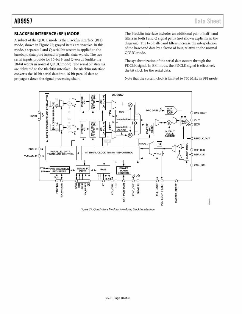
BLACKFIN INTERFACE (BFI) MODE A subset of the QDUC mode is the Blackfin interface (BFI) mode, shown in Figure 27; grayed items are inactive. In this mode, a separate I and Q serial bit stream is applied to the baseband data port instead of parallel data-words. The two serial inputs provide for 16-bit I- and Q-words (unlike the 18-bit words in normal QDUC mode). The serial bit streams are delivered to the Blackfin interface. The Blackfin interface converts the 16-bit serial data into 16-bit parallel data to propagate down the signal processing chain.
The Blackfin interface includes an additional pair of half-band filters in both I and Q signal paths (not shown explicitly in the diagram). The two half-band filters increase the interpolation of the baseband data by a factor of four, relative to the normal QDUC mode.
The synchronization of the serial data occurs through the PDCLK signal. In BFI mode, the PDCLK signal is effectively the bit clock for the serial data.
Note that the system clock is limited to 750 MHz in BFI mode.
0638
4-00
7
PDCLK
I/Q IN
EXT_
PWR
_DW
N
DAC_RSET
IOUT
IOUT
TxENABLE
DAC GAIN
θ
INVE
RSE
SIN
CFI
LTER
CLOCKFTW
PW8
SYSCLK
PLL
÷2
CLO
CK
MO
DE
REF_CLK
REF_CLK
REFCLK_OUT
XTAL_SEL
AD9957
ωcos (ωt+θ)
sin (ωt+θ)
SYN
C_O
UT
SYN
C_I
N
PLL_
LOC
K
PLL_
LOO
P_FI
LTER
MA
STER
_RES
ET2 2
OSK
DDSAUXDAC8-BIT
POWERDOWN
CONTROL
2
DAT
AA
SSEM
BLE
RA
ND
FO
RM
ATTE
R
I
Q
IS
QS
BLA
CK
FIN
INTE
RFA
CE
18
18
16
16 INVE
RSE
CC
IIN
VER
SEC
CI
OSK
INTERNAL CLOCK TIMING AND CONTROL
DAC14-BIT
CC
I_O
VFL
OSK
FTWPW
PARALLEL DATATIMING AND CONTROL
RT
RAM
PRO
FILE
SERIAL I/OPORT
I/O_U
PDAT
E
PROGRAMMINGREGISTERS
3I Q IS QS
HA
LF-B
AN
DFI
LTER
S (4
×)
CC
I(1
× TO
63×
)
HA
LF-B
AN
DFI
LTER
S (4
×)
CC
I(1
× TO
63×
)
OUTPUTSCALE
FACTOR
SDIO CS
I/O_R
ESET
SCLK
SDO
Figure 27. Quadrature Modulation Mode, Blackfin Interface

Data Sheet AD9957
Rev. F | Page 19 of 61
INTERPOLATING DAC MODE A block diagram of the AD9957 operating in interpolating DAC mode is shown in Figure 28; grayed items are inactive. In this mode, the Q data path, DDS, and modulator are all disabled; only the I data path is active.
As in quadrature modulation mode, the PDCLK pin functions as a clock, synchronizing the input of data to the AD9957.
No modulation takes place in the interpolating DAC mode; therefore, the spectrum of the data supplied at the parallel port remains at baseband. However, a sample rate conversion takes place based on the programmed interpolation rate. The inter-polation hardware processes the signal, effectively performing an oversample with a zero-stuffing operation. The original input spectrum remains intact and the images that otherwise would occur from the sample rate conversion process are suppressed by the interpolation signal chain.
0638
4-00
8
PDCLK
I/Q IN
EXT_
PWR
_DW
N
DAC_RSET
IOUT
IOUT
TxENABLE
DAC GAIN
θ
INVE
RSE
SIN
CFI
LTER
CLOCKFTW
PW
8
SYSCLK
PLL
÷2
CLO
CK
MO
DE
REF_CLK
REF_CLK
REFCLK_OUT
XTAL_SEL
PARALLEL DATATIMING AND CONTROL
AD9957
ωcos (ωt+θ)
sin (ωt+θ)
SYN
C_O
UT
SYN
C_I
N
PLL_
LOC
K
PLL_
LOO
P_FI
LTER
MA
STER
_RES
ET
2 2
DDSAUXDAC8-BIT
POWERDOWN
CONTROL
18
DAT
AA
SSEM
BLE
RA
ND
FO
RM
ATTE
R
I
Q
IS
QS
BLA
CK
FIN
INTE
RFA
CE
18
18
16
16H
ALF
-BA
ND
FILT
ERS
(4×)
INVE
RSE
CC
I
CC
I(1
× TO
63×
)
HA
LF-B
AN
DFI
LTER
S (4
×)
INVE
RSE
CC
I
CC
I(1
× TO
63×
)
OSK
INTERNAL CLOCK TIMING AND CONTROL
DAC14-BIT
FTWPW
OSKR
T
RAM
PRO
FILE
SERIAL I/OPORT
I/O_U
PDAT
E
PROGRAMMINGREGISTERS
3I Q IS QS
OUTPUTSCALE
FACTOR
CC
I_O
VFL
SDIO CS
I/O_R
ESET
SCLK
SDO
Figure 28. Interpolating DAC Mode

AD9957 Data Sheet
Rev. F | Page 20 of 61
SINGLE TONE MODE A block diagram of the AD9957 operating in single tone mode is shown in Figure 29; grayed items are inactive. In this mode, both I and Q data paths are disabled from the 18-bit parallel data port up to, and including, the modulator. The internal DDS core produces a single frequency signal based on the programmed tuning word. The user may select either the
cosine or sine output of the DDS. The sinusoid at the DDS output can be scaled using a 14-bit amplitude scale factor (ASF) and optionally routed through the inverse sinc filter.
Single tone mode offers the output shift keying (OSK) function. It provides the ability to ramp the amplitude scale factor between zero and an arbitrary preset value over a programmable time interval.
0638
4-00
9
PDCLK
I/Q IN
EXT_
PWR
_DW
N
DAC_RSET
IOUT
IOUT
TxENABLE
FTWPW
DAC GAIN
θ
INVE
RSE
SIN
CFI
LTER
CLOCKFTW
PW
8
SYSCLK
PLL
÷2
CLO
CK
MO
DE
REF_CLK
REF_CLK
REFCLK_OUT
XTAL_SEL
PARALLEL DATATIMING AND CONTROL
AD9957
ωcos (ωt+θ)
sin (ωt+θ)
SYN
C_O
UT
SYN
C_I
N
PLL_
LOC
K
PLL_
LOO
P_FI
LTER
MA
STER
_RES
ET
2 2
CC
I_O
VFL
OSK
DDSAUXDAC8-BIT
POWERDOWN
CONTROL
RT
RAM
PRO
FILE
SERIAL I/OPORT
I/O_U
PDAT
E
PROGRAMMINGREGISTERS
3I Q IS QS
10
DAT
AA
SSEM
BLE
RA
ND
FO
RM
ATTE
R
I
Q
IS
QS
BLA
CK
FIN
INTE
RFA
CE
18
18
16
16H
ALF
-BA
ND
FILT
ERS
(4×)
INVE
RSE
CC
I
CC
I(1
× TO
63×
)
HA
LF-B
AN
DFI
LTER
S (4
×)
INVE
RSE
CC
I
CC
I(1
× TO
63×
)
OSK
INTERNAL CLOCK TIMING AND CONTROL
DAC14-BIT
OUTPUTSCALE
FACTOR
SDIO CS
I/O_R
ESET
SCLK
SDO
Figure 29. Single Tone Mode

Data Sheet AD9957
Rev. F | Page 21 of 61
SIGNAL PROCESSING For a better understanding of the operation of the AD9957, it is helpful to follow the signal path in quadrature modulation mode from the parallel data port to the output of the DAC, examining the function of each block (see Figure 26).
The internal system clock (SYSCLK) signal that generates from the timing source provided to the REF_CLK pins provides all timing within the AD9957.
PARALLEL DATA CLOCK (PDCLK) The AD9957 generates a signal on the PDCLK pin, which is a clock signal that runs at the sample rate of the parallel data port. PDCLK serves as a data clock for the parallel port in QDUC and interpolating DAC modes; in BFI mode, it is a bit clock. Normally, the device uses the rising edges on PDCLK to latch the user-supplied data into the data port. Alternatively, the PDCLK Invert bit selects the falling edges as the active edges. Furthermore, the PDCLK enable bit is used to switch off the PDCLK signal. Even when the output signal is turned off via the PDCLK enable bit, PDCLK continues to operate internally. The device uses PDCLK internally to capture parallel data. Note that PDCLK is Logic 0 when disabled.
In QDUC mode, the AD9957 expects alternating I- and Q- data-words at the parallel port (see Figure 31). Each active edge of PDCLK captures one 18-bit word; therefore, there are two PDCLK cycles per I/Q pair. In BFI mode, the AD9957 expects two serial bit streams, each segmented into 16-bit words with PDCLK indicating each new bit. In either case, the output clock rate is fPDCLK as explained in the Input Data Assembler section.
In QDUC applications that require a consistent timing relation-ship between the internal SYSCLK signal and the PDCLK signal, the PDCLK rate control bit is used to slightly alter the operation of PDCLK. When this bit is set, the PDCLK rate is reduced by a factor of two. This causes rising edges on PDCLK to latch incoming I-words and falling edges to latch incoming Q-words. Again, the edge polarity assignment is reversible via the PDCLK Invert bit.
TRANSMIT ENABLE PIN (TxENABLE) The AD9957 accepts a user-generated signal applied to the TxENABLE pin that gates the user supplied data. Polarity of the TxENABLE pin is set using the TxENABLE invert bit (see the Register Map section for details). When TxENABLE is true, the device latches data into the device on the expected edge of PDCLK (based on the PDCLK invert bit). When TxENABLE is false, the device ignores the data supplied to the port, even though the PDCLK may continue to operate. Furthermore, when the TxENABLE pin is held false, then the device either forces the 18-bit data-words to Logic 0s, or it retains the last value present on the data port prior to TxENABLE switching to the false state (see the data assembler hold last value bit in the Register Map section).
Alternatively, rather than operating the TxENABLE pin as a gate for framing bursts of data, it can be driven with a clock signal operating at the parallel port data rate. When driven by a clock signal, the transition from the false to true state must meet the required setup and hold times on each cycle to ensure proper operation.
In QDUC mode, on the false-to-true edge of TxENABLE, the device is ready to receive the first I-word. The first I-word is latched into the device coincident with the active edge of PDCLK. The next active edge of PDCLK latches in a Q-word, and so on, until TxENABLE is returned to a static false state. The user may reverse the ordering of the I- and Q-words via the Q-First Data Pairing bit. Furthermore, the user must ensure that an even number of data words are delivered to the device as it must capture both an I- and a Q-word before the data is processed along the signal chain.
In interpolating DAC mode, TxENABLE operation is similar to QDUC mode, but without the need for I/Q data pairing; the even-number-of-PDCLK-cycles rule does not apply.
In BFI mode, operation of the TxENABLE pin is similar except that instead of the false-to-true edge marking the first I-word, it marks the first I and Q bits in a serial frame. The user must ensure that all 16-bits of a serial frame are delivered because the device must capture a full 16-bit I- and Q-word before the data is processed along the signal chain.
The timing relationships between TxENABLE, PDCLK, and DATA are shown in Figure 30, Figure 31, and Figure 32.

AD9957 Data Sheet
Rev. F | Page 22 of 61
tDH
I0
TxENABLE
PDCLK
D[17:0] IKIK – 1I3I2I1
0638
4-01
0
tDH
tDS
tDS
Figure 30. 18-Bit Parallel Port Timing Diagram—Interpolating DAC Mode
tDH
I0
TxENABLE
PDCLK
D[17:0] QNINQ1I1Q0
0638
4-01
1
tDH
tDS
tDS
Figure 31. 18-Bit Parallel Port Timing Diagram—Quadrature Modulation Mode
TxENABLE
PDCLK
I DATA
Q DATA Q0 Q1 Q2 Q3 Q4 Q6Q5 Q7 Q8 Q9 Q10 Q11 Q12 Q13 Q14 Q15
I0 I1 I2 I3 I4 I6I5 I7 I8 I9 I10 I11 I12 I13 I14 I15
I16n – 1
Q16n – 1
0638
4-01
2
Figure 32. Dual Serial I/Q Bit Stream Timing Diagram, BFI Mode
INPUT DATA ASSEMBLER The input to the AD9957 is an 18-bit parallel data port in QDUC mode or interpolating DAC mode. In BFI mode, it operates as a dual serial data port.
In QDUC mode, it is assumed that two consecutive 18-bit words represent the real (I) and imaginary (Q) parts of a complex number of the form, I + jQ. The 18-bit words are supplied to the input of the AD9957 at a rate of
Rf
f SYSCLKPDCLK 2
= for QDUC mode
where: fSYSCLK (for all of the PDCLK equations in this section) is the sample rate of the DAC. R (for all of the PDCLK equations in this section) is the interpolation factor of the programmable interpolation filter.
When the PDCLK rate control bit is active in QDUC mode, however, the frequency of PDCLK becomes
Rf
f SYSCLKPDCLK 4
= with PDCLK rate control active
In the interpolating DAC mode, the rate of PDCLK is the same as QDUC mode with the PDCLK rate control bit active, that is,
Rf
f SYSCLKPDCLK 4
= for interpolating DAC mode
In BFI mode, the 18-bit parallel input converts to a dual serial input that is, one pin is assigned as the serial input for the I-words and one pin is assigned as the serial input for the Q-words. The other 16 pins are not used. Furthermore, each I- and Q-word has a 16-bit resolution. fPDCLK is the bit rate of the I- and Q-data streams and is given by
Rf
f SYSCLKPDCLK = for BFI mode
Data Sheet AD9957
Rev. F | Page 23 of 61
Encoding and pulse shaping of symbols must be implemented before the data is presented to the input of the AD9957. Data delivered to the input of the AD9957 may be formatted as either twos complement or offset binary (see the Data Format bit in Table 13). In BFI mode, the bit sequence order can be set to either MSB-first or LSB-first (via the Blackfin Bit Order bit).
INVERSE CCI FILTER The inverse cascaded comb integrator (CCI) filter predistorts the data, compensating for the slight attenuation gradient imposed by the CCI filter (see the Programmable Interpolating Filter section). Data entering the first half-band filter occupies a maxi-mum bandwidth of ½ fIQ as defined by Nyquist (where fIQ is the sample rate at the input of the first half-band filter); see Figure 33.
If the CCI filter is used, the in-band attenuation gradient can pose a problem for applications requiring an extremely flat pass band. For example, if the spectrum of the data supplied to the AD9957 occupies a significant portion of the ½ fDATA region, the higher frequencies of the data spectrum are slightly more attenuated than the lower frequencies (the worst-case overall droop from f = 0 to ½ fDATA is <0.8 dB). The inverse CCI filter has a response characteristic that is the inverse of the CCI filter response over the ½ fIQ region.
INBANDATTENUATIONGRADIENT
CCI FILTER RESPONSE
½fIQ
fIQ 4fIQf
0638
4-01
3
Figure 33. CCI Filter Response
The product of the two responses yields an extremely flat pass band (±0.05 dB over the baseband Nyquist bandwidth) eliminating the in-band attenuation gradient introduced by the CCI filter. The cost is a slight attenuation of the input signal (approximately 0.5 dB for a CCI interpolation rate of 2, and 0.8 dB for higher interpolation rates).
The inverse CCI filter can be bypassed using the appropriate bit in the register map; it is automatically bypassed if the CCI inter-polation rate is 1×. When bypassed, power to the stage turns off to reduce power consumption.
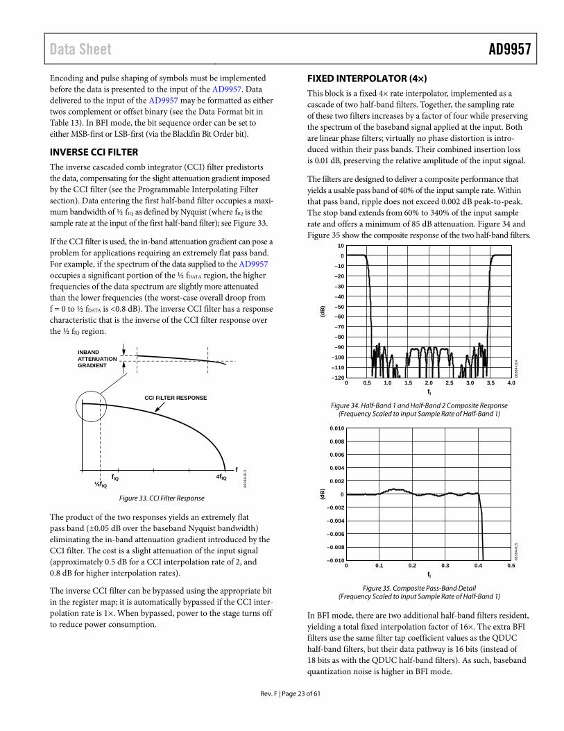
FIXED INTERPOLATOR (4×) This block is a fixed 4× rate interpolator, implemented as a cascade of two half-band filters. Together, the sampling rate of these two filters increases by a factor of four while preserving the spectrum of the baseband signal applied at the input. Both are linear phase filters; virtually no phase distortion is intro-duced within their pass bands. Their combined insertion loss is 0.01 dB, preserving the relative amplitude of the input signal.
The filters are designed to deliver a composite performance that yields a usable pass band of 40% of the input sample rate. Within that pass band, ripple does not exceed 0.002 dB peak-to-peak. The stop band extends from 60% to 340% of the input sample rate and offers a minimum of 85 dB attenuation. Figure 34 and Figure 35 show the composite response of the two half-band filters.
–120
–110
–100
–90
–80
–70
–60
–50
–40
–30
–20
–10
0
10
0 0.5 1.0 1.5 2.0 2.5 3.0 3.5 4.0
0638
4-01
4
(dB
)
fI Figure 34. Half-Band 1 and Half-Band 2 Composite Response
(Frequency Scaled to Input Sample Rate of Half-Band 1)
–0.010
–0.008
0.008
–0.006
0.006
–0.004
0.004
–0.002
0.002
0
0.010
0 0.1 0.2 0.3 0.4 0.5
0638
4-01
5
(dB
)
fI Figure 35. Composite Pass-Band Detail
(Frequency Scaled to Input Sample Rate of Half-Band 1)
In BFI mode, there are two additional half-band filters resident, yielding a total fixed interpolation factor of 16×. The extra BFI filters use the same filter tap coefficient values as the QDUC half-band filters, but their data pathway is 16 bits (instead of 18 bits as with the QDUC half-band filters). As such, baseband quantization noise is higher in BFI mode.

AD9957 Data Sheet
Rev. F | Page 24 of 61
Knowledge of the frequency response of the half-band filters is essential to understanding their impact on the spectral properties of the input signal. This is especially true when using the quad-rature modulator to upconvert a baseband signal containing complex data symbols that have been pulse shaped.
Consider that a complex symbol is represented by a real (I) and an imaginary (Q) component, thus requiring two digital words to represent a single complex sample of the form I + jQ. The sample rate associated with a sequence of complex symbols is referred to as fSYMBOL. If pulse shaping is applied to the symbols, the sample rate must be increased by some integer factor, M (a consequence of the pulse shaping process). This new sample rate (fIQ) is related to the symbol rate by
fIQ = MfSYMBOL
where fIQ is the rate at which complex samples must be supplied to the input of the first half-band filter in both (I and Q) signal paths. This rate should not be confused with the rate at which data is supplied to the AD9957.
Typically, pulse shaping is applied to the baseband symbols via a filter having a raised cosine response. In such cases, an excess bandwidth factor (α, 0 ≤ α ≤ 1) is used to modify the bandwidth of the data. For α = 0, the data bandwidth corresponds to fSYMBOL/2; for α = 1, the data bandwidth extends to fSYMBOL. Figure 36 shows the relationship between α, the bandwidth of the raised cosine response, and the response of the first half-band filter.
f
f
f
TYPICAL SPECTRUM OF A RANDOM SYMBOL SEQUENCE
RAISED COSINESPECTRAL MASK
SAMPLE RATE FOR2× OVERSAMPLEDPULSE SHAPING
INPUT SAMPLERATE OF FIRST
HALF-BANDFILTER
HALF-BANDFILTER
RESPONSEINPUT SAMPLERATE OF FIRST
HALF-BANDFILTER
NYQUISTBANDWIDTH
½fSYMBOL fSYMBOL 2fSYMBOL 3fSYMBOL
½fSYMBOL
0.4fIQ fIQ 2fIQ½fIQ
fSYMBOL 2fSYMBOL 4fSYMBOL
α = 1α = 0
α = 0.5
0638
4-01
6
Figure 36. Effect of the Excess Bandwidth Factor (α)
The responses in Figure 36 reflect the specific case of M = 2 (the interpolation factor for the pulse shaping operation). Increasing Factor M shifts the location of the fIQ point on the half-band
response portion of the diagram to the right, as it must remain aligned with the corresponding MfSYMBOL point on the frequency axis of the raised cosine spectral diagram. However, if fIQ shifts to the right, so does the half-band response, proportionally.
The result is that the raised cosine spectral mask always lies within the flat portion (dc to 0.4 fIQ) of the pass band response of the first half-band filter, regardless of the choice of α so long as M > 2. Therefore, for M > 2, the first half-band filter has absolutely no negative impact on the spectrum of the baseband signal when raised cosine pulse shaping is employed. For the case of M = 2, a problem can arise. This is highlighted by the shaded area in the tail of the α = 1 trace on the raised cosine spectral mask diagram. Notice that this portion of the raised cosine spectral mask extends beyond the flat portion of the half-band response and causes unwanted amplitude and phase distortion as the signal passes through the first half-band filter. To avoid this, simply ensure that α ≤ 0.6 when M = 2.
PROGRAMMABLE INTERPOLATING FILTER The programmable interpolator is implemented as a low-pass CCI filter. It is programmable by a 6-bit control word, giving a range of 2× to 63× interpolation.
The programmable interpolator is bypassed when programmed for an interpolation factor of 1. When bypassed, power to the stage is removed and the inverse CCI filter is also bypassed, because its compensation is not needed.
The output of the programmable interpolator is the data from the 4× interpolator further upsampled by the CCI filter, accord-ing to the rate chosen by the user. This results in the upsampling of the input data by a factor of 8× to 252× in steps of four.
The transfer function of the CCI interpolating filter is
( ) ( )5
1
0
2
= ∑
−
=
−R
k
fkπjefH (1)
where R is the programmed interpolation factor, and f is the frequency normalized to fSYSCLK.
Note that minimum R requirements exist depending on the mode and frequency of fSYSCLK. The minimum R setting is defined under the following conditions.
QDUC Mode
If fSYSCLK is between 500 MSPS to 1 GSPS, then the minimum R is 2.
If fSYSCLK is less than 500 MSPS, then the minimum R is 1.
BFI Mode
If fSYSCLK is between 500 MSPS to 750 MSPS, then the minimum R is 3.
If fSYSCLK is between 250 MSPS to 500 MSPS, then the minimum R is 2.
If fSYSCLK is less than 250 MSPS, then the minimum R is 1.

Data Sheet AD9957
Rev. F | Page 25 of 61
QUADRATURE MODULATOR The digital quadrature modulator stage shifts the frequency of the baseband spectrum of the incoming data stream up to the desired carrier frequency (a process known as upconversion).
At this point, the baseband data, which was delivered to the device at an I/Q sample rate of fIQ, has been upsampled to a rate equal to the frequency of SYSCLK, making the data sampling rate equal to the sampling rate of the carrier signal.
A direct digital synthesizer (DDS) controls the frequency of the carrier signal. The DDS very precisely generates the desired carrier frequency from the internal reference clock (SYSCLK). The carrier is applied to the I and Q multipliers in quadrature fashion (90° phase offset) and summed, yielding a data stream that represents the quadrature modulated carrier.
The modulation is performed digitally, avoiding the phase offset, gain imbalance, and crosstalk issues commonly associated with analog modulators. Note that the modulated, so-called signal is a number stream sampled at the rate of SYSCLK, the same rate at which the DAC is clocked.
A spectral invert bit controls the orientation of the modulated signal with respect to the carrier. This bit resides in each of the eight profile registers. By default, the time domain output of the quadrature modulator takes the form
I(t) × cos(ωt) − Q(t) × sin(ωt) (2)
When the spectral invert bit is asserted, it becomes
I(t) × cos(ωt) + Q(t) × sin(ωt) (3)
DDS CORE The direct digital synthesizer (DDS) block generates sine and/or cosine signals. In single tone mode, the DDS generates either a digital sine or cosine waveform based on the select DDS sine output bit. In QDUC mode, the DDS generates the quadra-ture carrier reference signal that digitally modulates the I/Q baseband signal.
The DDS output frequency is tuned using registers accessed via the serial I/O port. This allows for both precise tuning and instantaneous changing of the carrier frequency.
The equation relating output frequency (fOUT) of the DDS to the frequency tuning word (FTW) and the system clock (fSYSCLK) is
SYSCLKOUT fFTWf
= 322
(4)
where FTW is a decimal number from 0 to 2,147,483,647 (231 − 1).
Solving for FTW yields
=
SYSCLK
OUT
ff
roundFTW 322 (5)
where the round() function means to round the result to the nearest integer. For example, for fOUT = 41 MHz and fSYSCLK = 122.88 MHz, then FTW = 1,433,053,867 (0x556AAAAB).
In single tone mode, the DDS frequency, phase, and amplitude are all programmable via the serial I/O port. The amplitude is controlled by means of a digital multiplier using a 14-bit fractional scale value called the amplitude scale factor (ASF). The LSB weight is 2−14, yielding a multiplier range of 0 to 0.99993896484375 (1 − 2−14). To bypass the ASF multiplier, program the appropriate control register bit (see the details of CFR2, Bit 24 in the Register Bit Descriptions section). When bypassed, the ASF multiplier clocks are disabled to conserve power. The phase offset is controlled by means of a digital adder that uses a 14-bit offset value called the phase offset word (POW). The adder is situated between the phase accumulator and the angle-to-amplitude conversion logic in the DDS core. The adder applies the POW to the instantaneous phase values produced by the DDS phase accumulator. The adder is MSB aligned with the phase accumulator yielding an LSB weight of 2−14 (which equates to a resolution of ~0.022° or ~0.000383 radians). Both the ASF and the POW are available for each of the eight profiles.
INVERSE SINC FILTER The sampled carrier data stream is the input to the digital-to-analog converter. The DAC output spectrum is shaped by the characteristic sin(x)/x (or sinc) envelope, due to the intrinsic zero-order hold effect associated with DAC-generated signals. The shape of the sinc envelope is well known and can be compensated for. The inverse sinc filter preceding the DAC provides this compensation.
The inverse sinc filter is implemented as a digital FIR filter. Its response characteristic very nearly matches the inverse of the sinc envelope, as shown in Figure 37 (along with the sinc envelope for comparison).
The inverse sinc filter is enabled through a bit in the register map. The filter tap coefficients are listed in Table 4. The filter predistorts the data prior to its arrival at the DAC to compensate for the sinc envelope that otherwise distorts the spectrum.
When the inverse sinc filter is enabled, it introduces a ~3.0 dB insertion loss. The inverse sinc compensation is effective for output frequencies up to 40% (nominally) of the DAC sample rate.
Table 4. Inverse Sinc Filter Tap Coefficients Tap No. Tap Value Tap No. 1 −35 7 2 +134 6 3 −562 5 4 +6729 4

AD9957 Data Sheet
Rev. F | Page 26 of 61
In Figure 37, it can be seen that the sinc envelope introduces a frequency dependent attenuation that can be as much as 4 dB at the Nyquist frequency (half of the DAC sample rate). Without the inverse sinc filter, the DAC output also suffers from the frequency dependent droop of the sinc envelope. The inverse sinc filter effectively flattens the droop to within ±0.05 dB as shown in Figure 38, which shows the corrected sinc response with the inverse sinc filter enabled.
1
0
–1
–2
–3
–40 0.1 0.2 0.40.3 0.5
0638
4-01
7
(dB
)
FREQUENCY RELATIVE TO DAC SAMPLE RATE
INVERSESINC
SINC
Figure 37. Sinc and Inverse Sinc Responses
–2.8
–2.9
–3.0
–3.10 0.1 0.2 0.40.3 0.5
0638
4-01
8
(dB
)
FREQUENCY RELATIVE TO DAC SAMPLE RATE
COMPENSATED RESPONSE
Figure 38. DAC Response with Inverse Sinc Compensation
OUTPUT SCALE FACTOR (OSF) In QDUC and interpolating DAC modes, the output amplitude is controlled using an 8-bit digital multiplier. The 8-bit multiplier value is called the output scale factor (OSF) and is programmed via the appropriate control registers. It is available for each of the eight profiles. The LSB weight is 2−7, which yields a multiplier range of 0 to 1.9921875 (2 − 2−7). The gain extends to nearly a factor of 2 to provide a means to overcome the intrinsic loss through the modulator when operating in the quadrature modulation mode.
In interpolating DAC mode, the OSF should not be programmed to exceed unity, as clipping can result. Programming the 8-bit multiplier to unity gain (0x80) bypasses the stage and reduces power consumption.
14-BIT DAC The AD9957 incorporates an integrated 14-bit current-output DAC. The output current is delivered as a balanced signal using two outputs. The use of balanced outputs reduces the amount of common-mode noise at the DAC output, increasing signal-to-noise ratio. An external resistor (RSET) connected between the DAC_RSET pin and AGND establishes a reference current. The full-scale output current of the DAC (IOUT) is a scaled version of the reference current (see the Auxiliary DAC section that follows).
Proper attention should be paid to the load termination to keep the output voltage within the specified compliance range, as voltages developed beyond this range cause excessive distortion and can damage the DAC output circuitry.
Auxiliary DAC
The full-scale output current of the main DAC (IOUT) is con-trolled by an 8-bit auxiliary DAC. An 8-bit code word stored in the appropriate register map location sets IOUT according to the following equation:
+=
9614.86 CODE
RI
SETOUT (6)
where: RSET is the value of the RSET resistor (in ohms). CODE is the 8-bit value supplied to the auxiliary DAC (default is 127).
For example, with RSET = 10,000 and CODE = 127, IOUT = 20.07 mA.

Data Sheet AD9957
Rev. F | Page 27 of 61
RAM CONTROL RAM OVERVIEW The AD9957 has an integrated 1024 × 32-bit RAM. This RAM is only accessible when the AD9957 is operating in QDUC or interpolating DAC mode. The RAM has two fundamental modes of operation: data entry/retrieve mode and playback mode. The mode is selected by programming the RAM Enable bit in CFR1 via the serial I/O port.
Data entry/retrieve mode is used to load or read back the RAM contents via the serial I/O port. Playback mode is used to deliver RAM data to one of two internal destinations: the baseband scaling multipliers (see Figure 25, the IS and QS labels) or the baseband signal chain (see Figure 25, the I and Q labels). In both cases, the RAM can be used to apply an arbitrary, time-varying waveform to the selected destination. A block diagram of the RAM and its control elements is shown in Figure 39.
The external parallel data port is disabled when the baseband signal chain serves as the RAM playback destination.
RAM3210
QSTATEMACHINE SCLK
SDIOSDO
CSI/O_RESET
RT
END ADDRESSSTART ADDRESS10
10
ADDRESS STEP RATE16RAM MODE3
CLK
BASEBAND DATA CLOCK
I16
IS
Q
QS
DDS CLOCK
UP/DOWN COUNTER
I CHANNEL
Q CHANNEL
RAMSEGMENT
REGISTERS
SER
IAL
I/O P
OR
T
AD
DR
ESS
DA
TA
U/D 32
(MSBs)
(LSBs)
16
0638
4-01
9
Figure 39. RAM Block Diagram
In Figure 39, the serial I/O port is used to program the contents of the two RAM segment registers as well as to load and retrieve the RAM contents. The state machine takes care of incrementing or decrementing the RAM address locations and controlling the timing of the RAM address and data for proper operation. The I-channel and Q-channel multiplexers route RAM data to base-band scaling multipliers (IS/QS) or directly to the baseband signal chain (I/Q) when the RAM is used in playback mode. The state of the RAM playback destination bit determines the destination of the RAM data during playback.
An I/O update (or a profile change) is necessary to enact a state change of the RAM enable or RAM playback destination bits, or any of the RAM segment register bits.
The 32-bit RAM data bus is partitioned so that the 16 MSBs are designated as I-channel bits and the 16 LSBs are designated as
Q-channel bits. In playback mode, when driving data directly into the baseband signal chain, the 16-bit data-words are considered to be signed (that is, twos complement) values. The 16-bit I-and Q-words are MSB aligned with the 18-bit I and Q baseband data path. The two remaining LSBs of each 18-bit baseband channel are driven by the MSB of the respective channel. This ensures correct polarity coding when the 16-bit I and Q data from the RAM translates into 18-bit words for the baseband signal chain. Alternatively, when the RAM is driving the baseband scaling multipliers in playback mode, the RAM data is considered to represent unsigned, fractional values with a range of 0 to 1 − 2−16.
RAM SEGMENT REGISTERS Two dedicated registers (RAM Segment Register 0 and RAM Segment Register 1) control the operation of the RAM. Each contains the following:
• 10-bit start address word • 10-bit end address word • 16-bit address step rate word • 3-bit RAM playback mode word
When programming these registers, the user must ensure that the end address is greater than the start address.
With the RAM segment registers, the user can arbitrarily partition the RAM into two independent memory segments. The segment boundaries are specified with the start and end address words in each RAM segment register. The playback rate is controlled by the address step rate word (only meaningful when the base-band scaling multipliers serve as the playback destination). If the baseband signal chain serves as the RAM playback destination, the 16-bit address step rate words must be set to 1. The playback mode of the RAM is controlled via the RAM playback mode word.
RAM STATE MACHINE The state machine acts as an address generator for the RAM. Either the serial I/O port (when the RAM is operating in the load/retrieve mode) or the baseband data clock (when the RAM is in playback mode) clocks it. The state machine uses the RAM mode bits of the active RAM segment register to establish the proper sequence through the specified address range.
RAM TRIGGER (RT) PIN The RAM state machine monitors the RT pin for logic state tran-sitions. Any state transition triggers the state machine into action.
The direction of the logic state transition on the RT pin deter-mines which RAM segment register the state machine uses for playback instructions. RAM Segment Register 0 is used if the state machine detects a 0-to-1 transition; RAM Segment Register 1 is used if a 1-to-0 transition is detected.

AD9957 Data Sheet
Rev. F | Page 28 of 61
LOAD/RETRIEVE RAM OPERATION Loading or retrieving the RAM contents is a three-step process.
1. Program the RAM segment registers with start and end addresses defining the boundaries of each independent RAM segment.
2. Toggle the RT pin with the appropriate transition to select the desired RAM segment register.
3. Using the serial I/O port, write (or read) the address range specified by the selected RAM segment register.
Figure 40 shows the RAM block diagram when used for loading or retrieve operations.
RAM3210
QSTATEMACHINE
RT
END ADDRESSSTART ADDRESS10
10
ADDRESS STEP RATE16RAM MODE3
CLK
BASEBAND DATA CLOCK
I16
IS
Q
QS
DDS CLOCK
UP/DOWN COUNTER
I CHANNEL
Q CHANNEL
SER
IAL
I/O P
OR
T
AD
DR
ESS
DA
TA
U/D 32
(MSBs)
(LSBs)
16
0638
4-02
0
NOTES1. NONESSENTIAL FUNCTIONAL COMPONENTS ARE RENDERED IN GRAY.
RAMSEGMENT
REGISTERS
SCLK
SDIOSDO
CSI/O_RESET
Figure 40. RAM Load/Retrieve Operation
During a load or retrieve operation, the state machine controls an up/down counter to step through the required RAM locations. The counter is synchronized with the serial I/O port so that the serial/parallel conversion of the 32-bit words is correctly timed with the generation of the appropriate RAM address to properly execute the desired read or write operation. The up/down counter always increments through the address range during serial I/O port operations.
Because the RAM segment registers are completely independent, it is possible to define overlapping address ranges. However, doing so causes the overlapping address locations to be over-written by the most recent write operation. It is recommended that the user avoid defining overlapping address ranges.
RAM PLAYBACK OPERATION When the RAM has been loaded, it can be used for playback operation. The destination of the playback data is selected via the RAM playback destination bit. The active RAM segment register is selected by the appropriate transition of the RT pin. The active RAM segment register directs the internal state machine by defining the RAM address range occupied by the data and the RAM playback mode. It also defines the playback
rate when the playback destination is the baseband scaling multipliers.
Although RAM load/retrieve operations via the serial I/O port take precedence over playback, it is recommended that the user not attempt RAM access via the serial I/O port when the RAM enable bit is set.
Figure 41 is a block diagram showing the functional compo-nents used for RAM playback operation when the internal destination is the baseband scaling multipliers.
RAM3210
QSTATEMACHINE
RT
END ADDRESSSTART ADDRESS10
10
ADDRESS STEP RATE16RAM MODE3
CLK
BASEBAND DATA CLOCK
I16
IS
Q
QS
DDS CLOCK
UP/DOWN COUNTER
I CHANNEL
Q CHANNEL
RAMSEGMENT
REGISTERS
SER
IAL
I/O P
OR
T
AD
DR
ESS
DA
TA
U/D 32
(MSBs)
(LSBs)
16
0638
4-02
1
NOTES1. NONESSENTIAL FUNCTIONAL COMPONENTS ARE RENDERED IN GRAY.
SCLK
SDIOSDO
CSI/O_RESET
Figure 41. RAM Playback to Baseband Scaling Multipliers
During playback to the baseband scaling multipliers, the address step rate word in the active RAM segment register sets the rate at which RAM data samples are delivered to the multipliers. The following equations define the RAM sample rate and sample interval (Δt):
RMf
RateSampleRAM SYSCLK
4=
SYSCLKfRMt 4
=∆
where: R is the rate interpolation factor for the CCI filter. M is the 16-bit value of the address step rate word stored in the active RAM segment register.
If the RAM enable bit is set and the baseband scaling multi-pliers are selected as the playback destination, then assertion of an I/O update or profile change causes the multipliers to be driven with a static value of zero. A subsequent state change on the RT pin causes the multipliers to be driven by the data played back from the RAM instead of the static zero value.
Figure 42 is a block diagram showing RAM playback operation when the internal destination is the baseband data path. During playback to the baseband data path, the state machine increments/ decrements the RAM address at the baseband data rate (the address step rate must be set to 1).
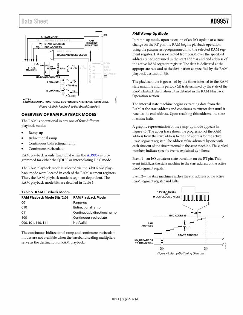
Data Sheet AD9957
Rev. F | Page 29 of 61
RAM3210
QSTATEMACHINE
RT
END ADDRESS
START ADDRESS10
10
ADDRESS STEP RATE16RAM MODE3
CLK
BASEBAND DATA CLOCK
I16
IS
Q
QS
DDS CLOCK
UP/DOWN COUNTER
I CHANNEL
Q CHANNEL
RAMSEGMENT
REGISTERS
SE
RIA
L I
/O P
OR
T
AD
DR
ES
S
DA
TAU/D 32
(MSBs)
(LSBs)
16
0638
4-02
2
NOTES1. NONESSENTIAL FUNCTIONAL COMPONENTS ARE RENDERED IN GRAY.
SCLK
SDIO
SDO
CS
I/O_RESET
Figure 42. RAM Playback to Baseband Data Path
OVERVIEW OF RAM PLAYBACK MODES The RAM is operational in any one of four different playback modes.
Ramp-up Bidirectional ramp Continuous bidirectional ramp Continuous recirculate
RAM playback is only functional when the AD9957 is pro-grammed for either the QDUC or interpolating DAC mode.
The RAM playback mode is selected via the 3-bit RAM play-back mode word located in each of the RAM segment registers. Thus, the RAM playback mode is segment dependent. The RAM playback mode bits are detailed in Table 5.
Table 5. RAM Playback Modes RAM Playback Mode Bits[2:0] RAM Playback Mode 001 Ramp-up 010 Bidirectional ramp
011 Continuous bidirectional ramp
100 Continuous recirculate
000, 101, 110, 111 Not Valid
The continuous bidirectional ramp and continuous recirculate modes are not available when the baseband scaling multipliers serve as the destination of RAM playback.
RAM Ramp-Up Mode
In ramp-up mode, upon assertion of an I/O update or a state change on the RT pin, the RAM begins playback operation using the parameters programmed into the selected RAM seg-ment register. Data is extracted from RAM over the specified address range contained in the start address and end address of the active RAM segment register. The data is delivered at the appropriate rate and to the destination as specified by the RAM playback destination bit.
The playback rate is governed by the timer internal to the RAM state machine and its period (Δt) is determined by the state of the RAM playback destination bit as detailed in the RAM Playback Operation section.
The internal state machine begins extracting data from the RAM at the start address and continues to extract data until it reaches the end address. Upon reaching this address, the state machine halts.
A graphic representation of the ramp-up mode appears in Figure 43. The upper trace shows the progression of the RAM address from the start address to the end address for the active RAM segment register. The address value advances by one with each timeout of the timer internal to the state machine. The circled numbers indicate specific events, explained as follows:
Event 1—an I/O update or state transition on the RT pin. This event initializes the state machine to the start address of the active RAM segment register.
Event 2—the state machine reaches the end address of the active RAM segment register and halts.
START ADDRESS
RAMADDRESS
END ADDRESS
1
1 PDCLK CYCLEOR
M DDS CLOCK CYCLES
∆t
I/O_UPDATE ORRT TRANSITION
21 0638
4-02
3
Figure 43. Ramp-Up Timing Diagram
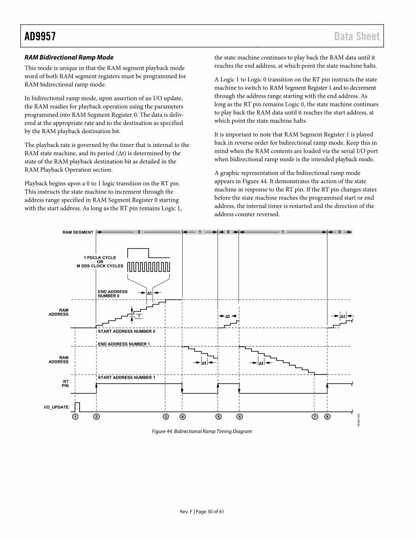
AD9957 Data Sheet
Rev. F | Page 30 of 61
RAM Bidirectional Ramp Mode
This mode is unique in that the RAM segment playback mode word of both RAM segment registers must be programmed for RAM bidirectional ramp mode.
In bidirectional ramp mode, upon assertion of an I/O update, the RAM readies for playback operation using the parameters programmed into RAM Segment Register 0. The data is deliv-ered at the appropriate rate and to the destination as specified by the RAM playback destination bit.
The playback rate is governed by the timer that is internal to the RAM state machine, and its period (Δt) is determined by the state of the RAM playback destination bit as detailed in the RAM Playback Operation section.
Playback begins upon a 0 to 1 logic transition on the RT pin. This instructs the state machine to increment through the address range specified in RAM Segment Register 0 starting with the start address. As long as the RT pin remains Logic 1,
the state machine continues to play back the RAM data until it reaches the end address, at which point the state machine halts.
A Logic 1 to Logic 0 transition on the RT pin instructs the state machine to switch to RAM Segment Register 1 and to decrement through the address range starting with the end address. As long as the RT pin remains Logic 0, the state machine continues to play back the RAM data until it reaches the start address, at which point the state machine halts.
It is important to note that RAM Segment Register 1 is played back in reverse order for bidirectional ramp mode. Keep this in mind when the RAM contents are loaded via the serial I/O port when bidirectional ramp mode is the intended playback mode.
A graphic representation of the bidirectional ramp mode appears in Figure 44. It demonstrates the action of the state machine in response to the RT pin. If the RT pin changes states before the state machine reaches the programmed start or end address, the internal timer is restarted and the direction of the address counter reversed.
1 2 3 4 5 6 7 8
0638
4-02
4
1
RAM SEGMENT 0 1 0 1 0
∆t
∆t
∆t ∆t
∆t
START ADDRESS NUMBER 1
START ADDRESS NUMBER 0
END ADDRESS NUMBER 1
END ADDRESSNUMBER 0
RAMADDRESS
RAMADDRESS
RTPIN
1 PDCLK CYCLEOR
M DDS CLOCK CYCLES
I/O_UPDATE
Figure 44. Bidirectional Ramp Timing Diagram

Data Sheet AD9957
Rev. F | Page 31 of 61
The circled numbers in Figure 44 indicate specific events, explained as follows:
Event 1—an I/O update or profile change activates the RAM bidirectional ramp mode.
Event 2—the RT pin switches to Logic 1. The state machine initializes to the start address of RAM Segment Register 0 and begins incrementing the RAM address counter.
Event 3—the RT pin remained at Logic 1 long enough for the state machine to reach the end address of RAM Segment Register 0, at which point the address counter is halted.
Event 4—the RT pin switches to Logic 0. The state machine initializes to the end address of RAM Segment Register 1, resets the internal timer, and begins decrementing the RAM address counter.
Event 5—the RT pin switches to Logic 1. The state machine initializes to the start address of RAM Segment Register 0, resets the internal timer, and begins incrementing the RAM address counter.
Event 6—the RT pin switches to Logic 0. The state machine initializes to the end address of RAM Segment Register 1, resets the internal timer, and begins decrementing the RAM address counter.
Event 7—the RT pin remained at Logic 0 long enough for the state machine to reach the start address of RAM Segment Register 1, at which point the address counter is halted.
Event 8—the RT pin switches to Logic 1. The state machine initializes to the start address of RAM Segment Register 0, resets the internal timer, and begins incrementing the RAM address counter.
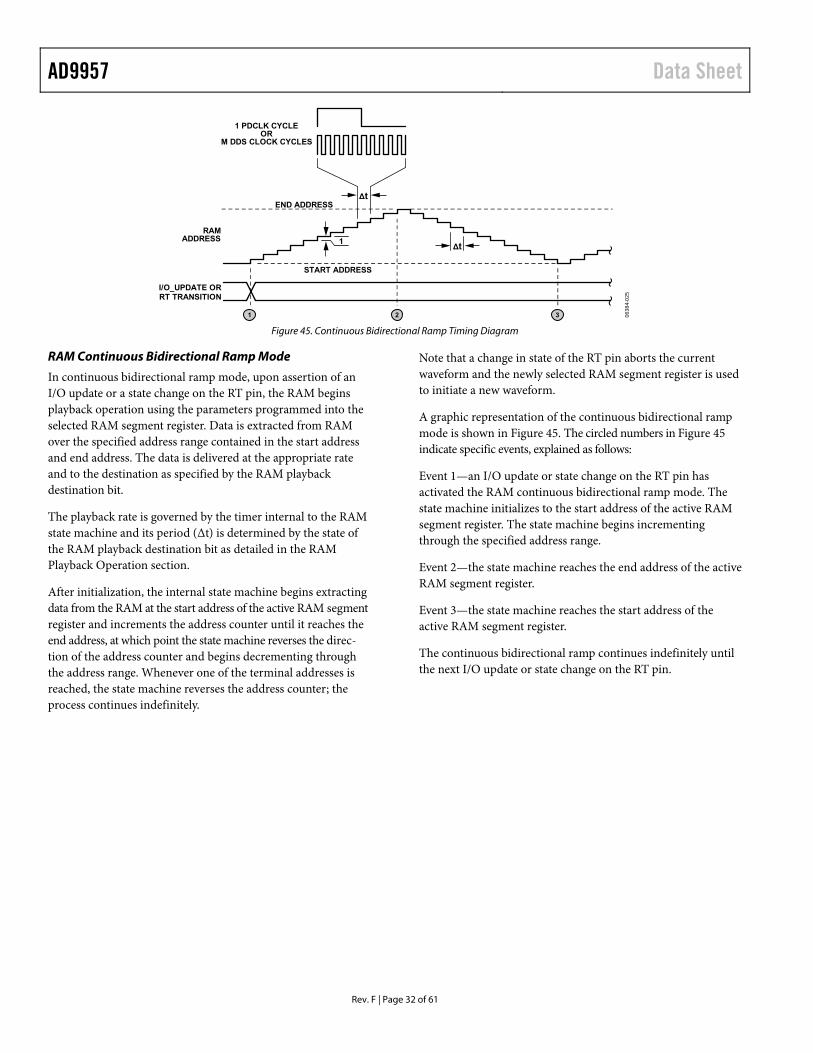
AD9957 Data Sheet
Rev. F | Page 32 of 61
START ADDRESS
RAMADDRESS
END ADDRESS
1
1 PDCLK CYCLEOR
M DDS CLOCK CYCLES
∆t
I/O_UPDATE ORRT TRANSITION
2 31
∆t
0638
4-02
5
Figure 45. Continuous Bidirectional Ramp Timing Diagram
RAM Continuous Bidirectional Ramp Mode
In continuous bidirectional ramp mode, upon assertion of an I/O update or a state change on the RT pin, the RAM begins playback operation using the parameters programmed into the selected RAM segment register. Data is extracted from RAM over the specified address range contained in the start address and end address. The data is delivered at the appropriate rate and to the destination as specified by the RAM playback destination bit.
The playback rate is governed by the timer internal to the RAM state machine and its period (Δt) is determined by the state of the RAM playback destination bit as detailed in the RAM Playback Operation section.
After initialization, the internal state machine begins extracting data from the RAM at the start address of the active RAM segment register and increments the address counter until it reaches the end address, at which point the state machine reverses the direc-tion of the address counter and begins decrementing through the address range. Whenever one of the terminal addresses is reached, the state machine reverses the address counter; the process continues indefinitely.
Note that a change in state of the RT pin aborts the current waveform and the newly selected RAM segment register is used to initiate a new waveform.
A graphic representation of the continuous bidirectional ramp mode is shown in Figure 45. The circled numbers in Figure 45 indicate specific events, explained as follows:
Event 1—an I/O update or state change on the RT pin has activated the RAM continuous bidirectional ramp mode. The state machine initializes to the start address of the active RAM segment register. The state machine begins incrementing through the specified address range.
Event 2—the state machine reaches the end address of the active RAM segment register.
Event 3—the state machine reaches the start address of the active RAM segment register.
The continuous bidirectional ramp continues indefinitely until the next I/O update or state change on the RT pin.

Data Sheet AD9957
Rev. F | Page 33 of 61
0638
4-02
6
START ADDRESS
END ADDRESS
1
1 2 3 4 5
RAM ADRESS
∆t
1 PDCLK CYCLEOR
M DDS CLOCK CYCLES
I/O_UPDATE ORRT TRANSITION
Figure 46. Continuous Recirculate Timing Diagram
RAM Continuous Recirculate Mode
The continuous recirculate mode mimics ramp-up mode, except that when the state machine reaches the end address of the active RAM segment register, it does not halt. Instead, the next timeout of the internal timer causes the state machine to jump to the start address of the active RAM segment register. This process continues indefinitely until an I/O update or state change on the RT pin. A state change on the RT pin aborts the current waveform and the newly selected RAM segment register initiates a new waveform.
A graphic representation of the continuous recirculate mode is shown in Figure 46.
The circled numbers in Figure 46 indicate specific events, which are explained as follows:
Event 1—an I/O update or state change on the RT pin occurs. This initializes the state machine to the start address of the
active RAM segment register and causes the state machine to begin incrementing the address counter at the appropriate rate.
Event 2—the state machine reaches the end address of the active RAM segment register.
Event 3—the state machine switches to the start address of the active RAM segment register. The state machine continues to increment the address counter.
Event 4—the state machine again reaches the end address of the active RAM segment register.
Event 5—the state machine switches to the start address of the active RAM segment register. The state machine continues to increment the address counter.
Event 4 and Event 5 repeat until an I/O update or state change occurs on the RT pin.
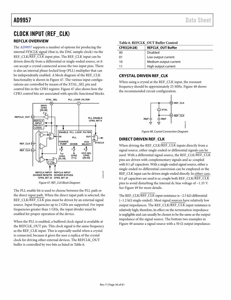
AD9957 Data Sheet
Rev. F | Page 34 of 61
CLOCK INPUT (REF_CLK) REFCLK OVERVIEW The AD9957 supports a number of options for producing the internal SYSCLK signal (that is, the DAC sample clock) via the REF_CLK/REF_CLK input pins. The REF_CLK input can be driven directly from a differential or single-ended source, or it can accept a crystal connected across the two input pins. There is also an internal phase-locked loop (PLL) multiplier that can be independently enabled. A block diagram of the REF_CLK functionality is shown in Figure 47. The various input configu-rations are controlled by means of the XTAL_SEL pin and control bits in the CFR3 register. Figure 47 also shows how the CFR3 control bits are associated with specific functional blocks.
REF_CLK
REF_CLK
PLL
VCOSELECTDIVIDE
CHARGEPUMP
OUTIN
PLL_LOOP_FILTERENABLE
PLL_LOOP_FILTER
DRV0CFR3
[29:28]
REFCLK_OUT
XTAL_SEL
REFCLKINPUT
SELECTLOGIC
SYSCLK
ICPCFR3
[21:19]
NCFR3[7:1]
VCO SELCFR3
[26:24]
÷2
REFCLK INPUTDIVIDER BYPASSCFR3, BIT 15
PLL ENABLECFR3, BIT 8
REFCLK INPUTDIVIDER RESETB
CFR3, BIT 14
94
95 2
90
91
01
01
2
2
7 3
01
0638
4-02
8
Figure 47. REF_CLK Block Diagram
The PLL enable bit is used to choose between the PLL path or the direct input path. When the direct input path is selected, the REF_CLK/REF_CLK pins must be driven by an external signal source. Input frequencies up to 2 GHz are supported. For input frequencies greater than 1 GHz, the input divider must be enabled for proper operation of the device.
When the PLL is enabled, a buffered clock signal is available at the REFCLK_OUT pin. This clock signal is the same frequency as the REF_CLK input. This is especially useful when a crystal is connected, because it gives the user a replica of the crystal clock for driving other external devices. The REFCLK_OUT buffer is controlled by two bits as listed in Table 6.
Table 6. REFCLK_OUT Buffer Control CFR3[29:28] REFCLK_OUT Buffer 00 Disabled 01 Low output current 10 Medium output current 11 High output current
CRYSTAL DRIVEN REF_CLK When using a crystal at the REF_CLK input, the resonant frequency should be approximately 25 MHz. Figure 48 shows the recommended circuit configuration.
0638
4-02
7
REF_CLK
REF_CLK39pF39pF
XTAL
90
91
Figure 48. Crystal Connection Diagram
DIRECT DRIVEN REF_CLK
When driving the REF_CLK/REF_CLK inputs directly from a signal source, either single-ended or differential signals can be used. With a differential signal source, the REF_CLK/REF_CLK pins are driven with complementary signals and ac-coupled with 0.1 µF capacitors. With a single-ended signal source, either a single-ended-to-differential conversion can be employed or the REF_CLK input can be driven single-ended directly. In either case, 0.1 µF capacitors are used to ac couple both REF_CLK/REF_CLK pins to avoid disturbing the internal dc bias voltage of ~1.35 V. See Figure 49 for more details.
The REF_CLK/REF_CLK input resistance is ~2.5 kΩ differential (~1.2 kΩ single-ended). Most signal sources have relatively low output impedances. The REF_CLK/REF_CLK input resistance is relatively high; therefore, its effect on the termination impedance is negligible and can usually be chosen to be the same as the output impedance of the signal source. The bottom two examples in Figure 49 assume a signal source with a 50 Ω output impedance.

Data Sheet AD9957
Rev. F | Page 35 of 61
0638
4-02
9
TERMINATION
REF_CLK
DIFFERENTIAL SOURCE,DIFFERENTIAL INPUT.
SINGLE-ENDED SOURCE,DIFFERENTIAL INPUT.
SINGLE-ENDED SOURCE,SINGLE-ENDED INPUT.
90
91
0.1µF
0.1µF
PECL,LVPECL,
ORLVDS
DRIVER
REF_CLK90
91
50Ω
0.1µF
0.1µF
BALUN(1:1)
REF_CLK
REF_CLK
REF_CLK
REF_CLK
90
910.1µF
0.1µF
50Ω
Figure 49. Direct Connection Diagram
PHASE-LOCKED LOOP (PLL) MULTIPLIER An internal phase-locked loop (PLL) provides users of the AD9957 the option to use a reference clock frequency that is significantly lower than the system clock frequency. The PLL supports a wide range of programmable frequency multiplica-tion factors (12× to 127×) as well as a programmable charge pump current and external loop filter components (connected via the PLL_LOOP_FILTER pin). These features add an extra layer of flexibility to the PLL, allowing optimization of phase noise performance and flexibility in frequency plan develop-ment. The PLL is also equipped with a PLL_LOCK pin.
The PLL output frequency range (fSYSCLK) is constrained to the range of 420 MHz ≤ fSYSCLK ≤ 1 GHz by the internal VCO. In addition, the user must program the VCO to one of six operating ranges such that fSYSCLK falls within the specified range. Figure 50 and Figure 51 summarize these VCO ranges.
Figure 50 shows the boundaries of the VCO frequency ranges over the full range of temperature and supply voltage variation for all devices from the available population. The implication is that multiple devices chosen at random from the population and operated under widely varying conditions may require different values to be programmed into CFR3[26:24] to operate at the same frequency. For example, Part A chosen randomly from the population, operating in an ambient temperature of −10°C with a system clock frequency of 900 MHz may require CFR3[26:24] to be set to 100b. Whereas Part B chosen randomly from the population, operating in an ambient temperature of 90°C with a system clock frequency of 900 MHz may require CFR3[26:24] to be set to 101b. If a frequency plan is chosen such that the system clock frequency operates within one set of boundaries (as shown in Figure 51), the required value in CFR3[26:24] is consistent from part to part.
Figure 51 shows the boundaries of the VCO frequency ranges over the full range of temperature and supply voltage variation for an individual device selected from the population. Figure 51 shows that the VCO frequency ranges for a single device always overlap when operated over the full range of conditions.
In conclusion, if a user wants to retain a single default value for CFR3[26:24], a frequency that falls into one of the ranges found in Figure 50 should be selected. Additionally, for any given individual device, the VCO frequency ranges overlap, meaning that any given device exhibits no gaps in its frequency coverage across VCO ranges over the full range of conditions.
0638
4-05
7
VCO0
VCO1
VCO2
VCO3
VCO4
VCO5
395 495 595 695 795 895 995
FLOW = 400FHIGH = 460
FLOW = 455FHIGH = 530
FLOW = 530FHIGH = 615
FLOW = 760FHIGH = 875
FLOW = 920FHIGH = 1030
FLOW = 650FHIGH = 790
(MHz) Figure 50. VCO Ranges Including Atypical Wafer Process Skew
335 435 535 635 735 835 935 1035 1135
VCO0
VCO1
VCO2
VCO3
VCO4
VCO5
0638
4-05
6
FLOW = 342FHIGH = 522
FLOW = 402FHIGH = 602
FLOW = 469FHIGH = 709
FLOW = 574FHIGH = 904
(MHz)
FLOW = 646FHIGH = 966
FLOW = 810FHIGH = 1180
Figure 51. Typical VCO Ranges
Table 7. VCO Range Bit Settings VCO SEL Bits (CFR3[26:24]) VCO Range
000 VCO0 001 VCO1 010 VCO2 011 VCO3 100 VCO4 101 VCO5 110 PLL Bypassed 111 PLL Bypassed
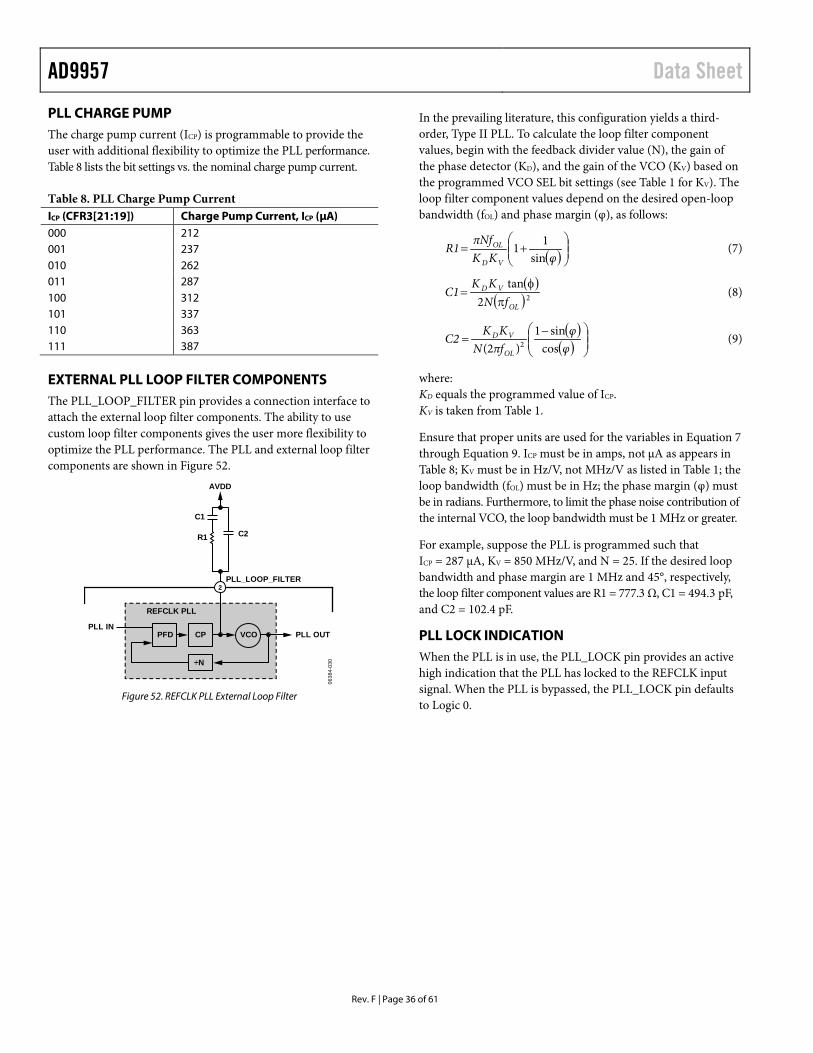
AD9957 Data Sheet
Rev. F | Page 36 of 61
PLL CHARGE PUMP The charge pump current (ICP) is programmable to provide the user with additional flexibility to optimize the PLL performance. Table 8 lists the bit settings vs. the nominal charge pump current.
Table 8. PLL Charge Pump Current ICP (CFR3[21:19]) Charge Pump Current, ICP (µA) 000 212 001 237 010 262 011 287 100 312 101 337 110 363 111 387
EXTERNAL PLL LOOP FILTER COMPONENTS The PLL_LOOP_FILTER pin provides a connection interface to attach the external loop filter components. The ability to use custom loop filter components gives the user more flexibility to optimize the PLL performance. The PLL and external loop filter components are shown in Figure 52.
PFD CP
PLL_LOOP_FILTER
VCO
÷N
PLL OUTPLL IN
AVDD
REFCLK PLL
2
R1
C1
C2
0638
4-03
0
Figure 52. REFCLK PLL External Loop Filter
In the prevailing literature, this configuration yields a third-order, Type II PLL. To calculate the loop filter component values, begin with the feedback divider value (N), the gain of the phase detector (KD), and the gain of the VCO (KV) based on the programmed VCO SEL bit settings (see Table 1 for KV). The loop filter component values depend on the desired open-loop bandwidth (fOL) and phase margin (φ), as follows:
( )
+=
φKKNfπ
R1VD
OL
sin11 (7)
( )( )22
tan
OL
VD
fNKK
C1π
φ= (8)
( )( )
−=
φφ
fπNKK
C2OL
VD
cossin1
)2( 2 (9)
where: KD equals the programmed value of ICP. KV is taken from Table 1.
Ensure that proper units are used for the variables in Equation 7 through Equation 9. ICP must be in amps, not µA as appears in Table 8; KV must be in Hz/V, not MHz/V as listed in Table 1; the loop bandwidth (fOL) must be in Hz; the phase margin (φ) must be in radians. Furthermore, to limit the phase noise contribution of the internal VCO, the loop bandwidth must be 1 MHz or greater.
For example, suppose the PLL is programmed such that ICP = 287 µA, KV = 850 MHz/V, and N = 25. If the desired loop bandwidth and phase margin are 1 MHz and 45°, respectively, the loop filter component values are R1 = 777.3 Ω, C1 = 494.3 pF, and C2 = 102.4 pF.
PLL LOCK INDICATION When the PLL is in use, the PLL_LOCK pin provides an active high indication that the PLL has locked to the REFCLK input signal. When the PLL is bypassed, the PLL_LOCK pin defaults to Logic 0.

Data Sheet AD9957
Rev. F | Page 37 of 61
ADDITIONAL FEATURES OUTPUT SHIFT KEYING (OSK) The OSK function (Figure 53) is only available in single tone mode. It allows the user to control the output signal amplitude of the DDS. Both manual and automatic modes are available.
0638
4-03
1
OSK ENABLE
AMPLITUDE SCALE FACTOR(ASF[15:2])
AMPLITUDE RAMP RATE(ASF[31:16])
AMPLITUDE STEP SIZE(ASF[1:0])
MANUAL OSK EXTERNAL
AUTO OSK ENABLE
OSK
DDS CLOCK
TO DDSAMPLITUDECONTROLPARAMETER
60
LOAD ARR AT I/O_UPDATE
OSKCONTROLLER
1416
14
2
Figure 53. OSK Block Diagram
Four control register bits, the external OSK pin, and the entire 32 bits of the ASF register govern the operation of the OSK function. The primary control for the OSK block is the OSK enable bit. When this bit is set, the OSK function is enabled; otherwise, the OSK function is disabled. When disabled, the other OSK input controls are ignored and the internal clocks are shut down to conserve power.
When the OSK function is enabled, automatic and manual operation is selected via the Select Auto-OSK bit. When this bit is set, the automatic mode is active; otherwise, the manual mode is active.
Manual OSK
In manual mode, output amplitude is varied by successive write operations to the amplitude scale factor portion of the ASF register. The rate at which amplitude changes can be applied to the output signal is limited by the speed of the serial I/O port. In manual mode, the OSK pin functionality depends on the state of the manual OSK external control bit. It is either inoperative or used to switch the output amplitude between the programmed amplitude scale factor value and zero. When operational, a Logic 0 on the OSK pin forces the output amplitude to zero whereas a Logic 1 on the OSK pin causes the output amplitude to be scaled by the amplitude scale factor value.
Automatic OSK
In automatic mode, the OSK function automatically generates a linear amplitude vs. time profile (or amplitude ramp). The amplitude ramp is controlled via three parameters, as follows:
• The maximum amplitude scale factor • The amplitude step size • The time interval between steps
The amplitude ramp parameters reside in the 32-bit ASF register and are programmed via the serial I/O port. The amplitude step interval is set using the 16-bit amplitude ramp rate portion of the ASF register (Bits[31:16]). The maximum amplitude scale factor is set using the 14-bit amplitude scale factor in the ASF register (Bits[15:2]). The amplitude step size is set using the 2-bit amplitude step size portion of the ASF register (Bits[1:0]). The direction of the ramp (positive or negative slope) is controlled by the external OSK pin. When the OSK pin is a Logic 1, the slope is positive; otherwise, it is negative.
A 16-bit programmable timer that is clocked at a rate of ¼ fSYSCLK controls the step interval. The timer period sets the interval between amplitude steps. The step time interval (Δt) is given by
SYSCLKfMt 4
=∆
where M is the 16-bit number stored in the amplitude ramp rate portion of the ASF register. For example, if fSYSCLK = 750 MHz and M = 23,218 (0x5AB2), then Δt ≈ 123.8293 µs.
The output of the OSK function is a 14-bit unsigned data bus that controls the amplitude of the DDS output (as long as the OSK enable bit is Logic 1). When the OSK pin is Logic 1, the OSK output value starts at 0 and increments by the programmed amplitude step size until it reaches the programmed maximum amplitude value. When the OSK pin is Logic 0, the OSK output starts at its present value and decrements by the programmed amplitude step size until it reaches 0.
The OSK output does not necessarily attain the maximum amplitude—the OSK pin may switch to Logic 0 before attaining the maximum value.
The OSK output does not necessarily reach a value of zero—the OSK pin may switch to Logic 1 before attaining the zero value.
The OSK output is initialized to 0 at power-up. It is also set to 0 when the OSK enable bit is Logic 0 or when the OSK enable bit is Logic 1, but the Select Auto-OSK bit is Logic 0.
The amplitude step size of the OSK output is set by the amplitude step size bits in the ASF register according to the values listed in Table 9. The step size refers to the LSB weight of the 14-bit OSK output.
The OSK output cannot exceed the maximum amplitude value programmed into the ASF register.

AD9957 Data Sheet
Rev. F | Page 38 of 61
Table 9. OSK Amplitude Step Size ASF[1:0] Amplitude Step Size 00 1 01 2 10 4 11 8
As mentioned earlier, the step interval is controlled by a 16-bit programmable timer. Normally, this timer is loaded with the programmed timing value whenever the timer expires, thus initiating a new timing cycle. However, three events cause the timer to have its timing value reloaded prior to the timer expiring. One such event is when the Select Auto-OSK bit is transitioned from a Logic 0 state to a Logic 1 state followed by an I/O update. A second such event is a change of state in the OSK pin. The third event is dependent on the status of the Load ARR at I/O Update bit. If this bit is Logic 0, no action occurs; otherwise, when the I/O_UPDATE pin is asserted (or a profile change occurs), the timer resets to its initial starting point.
PROFILES Each of the three operating modes of the AD9957 support the use of profiles, which consist of a group of registers containing pertinent operating parameters for a particular operating mode. Profiles enable rapid switching between parameter sets. Profile parameters are programmed via the serial I/O port. Once programmed, a specific profile is activated by means of three external pins (PROFILE2 to PROFILE0). A particular profile is activated by providing the appropriate logic levels to the profile control pins per the settings listed in Table 10.
Table 10. Profile Control Pins PROFILE2, PROFILE1, and PROFILE 0 Active Profile 000 0 001 1 010 2 011 3 100 4 101 5 110 6 111 7
Consider an application of basic two-tone frequency shift keying (FSK) where binary data is transmitted by selecting between two different frequencies: a mark frequency (Logic 1) and a space frequency (Logic 0). To accommodate FSK, the Profile 0 register is programmed with the appropriate frequency tuning word for a space, and the Profile 1 register is programmed with the appropriate frequency tuning word for a mark. Then, with the PROFILE1 and PROFILE2 pins tied to Logic 0, the PROFILE0 pin is used to transmit the data bits. The logic state of the PROFILE0 pin causes the appropriate mark and space frequencies to be generated.
I/O_UPDATE PIN By default, the I/O_UPDATE pin is an input that serves as a strobe signal to allow synchronous update of the device operating parameters. For example, frequency, phase, and amplitude con-trol words for the DDS can be programmed using the serial I/O port. However, the serial I/O port is an asynchronous interface; consequently, programming of the device operating parameters using the I/O port is not synchronized with the internal timing. Using the pin, I/O_UPDATE, the user can synchronize the application of certain programmed operating parameters with external circuitry when new parameters are programmed into the I/O registers. A rising edge on I/O_UPDATE initiates transfer of the register contents to the internal workings of the device.
The transfer of programmed data from the programming registers to the internal hardware is also accomplished by changing the state of the PROFILE2, PROFILE1, and PROFILE0 pins.
AUTOMATIC I/O UPDATE The AD9957 offers an option whereby the I/O update function is asserted automatically rather than relying on an external signal supplied by the user. This feature is enabled by setting the Internal I/O Update Active bit in CFR2.
When this feature is active, the I/O_UPDATE pin becomes an output pin. It generates an active high pulse each time an inter-nal I/O update occurs. The duration of the pulse is approximately 12 cycles of SYSCLK. This I/O update strobe can be used to notify an external controller that the device has generated an I/O update internally.
The repetition rate of the internal I/O update is programmed via the serial I/O port. Two parameters control the repetition rate. The first parameter consists of the two I/O update rate control bits in CFR2. The second parameter is the 32-bit word in the I/O update rate register that sets the range of an internal counter.
The I/O update rate control bits establish a divide by 1, 2, 4, or 8 of a clock signal that runs at ¼ fSYSCLK. The output of the divider clocks the aforementioned 32-bit internal counter. The repetition rate of the I/O update is given by
Bf
f ASYSCLK
UPDATEOI 2_/ =
where: A is the value of the 2-bit word comprising the I/O update rate control bits. B is the value of the 32-bit word stored in the I/O update rate register.
If B is programmed to 0x0003 or less, the I/O_UPDATE pin no longer pulses, but assumes a static Logic 1 state.

Data Sheet AD9957
Rev. F | Page 39 of 61
POWER-DOWN CONTROL The AD9957 offers the ability to independently power down four specific sections of the device. Power-down functionality applies to the digital core, DAC, auxiliary DAC, and REFCLK input.
A power-down of the digital core disables the ability to update the serial I/O port. However, the digital power-down bit can still be cleared via the serial port to prevent the possibility of a nonrecoverable state.
Software power-down is controlled through four independent power-down bits in CFR1. Software control requires forcing the EXT_PWR_DWN pin to a Logic 0 state. In this case, setting the desired power-down bits (via the serial I/O port) powers down the associated functional block; clearing the bits restores the function.
Alternatively, all four functions can be simultaneously powered down via external hardware control through the EXT_PWR_DWN pin. Forcing this pin to Logic 1 powers down all four circuit blocks, regardless of the state of the power-down bits. That is, the independent power-down bits in CFR1 are ignored and overridden when EXT_PWR_DWN is Logic 1.
Based on the state of the external power-down control bit, the EXT_PWR_DWN pin produces either a full power-down or a fast recovery power-down. The fast recovery power-down mode maintains power to the DAC bias circuitry and the PLL, VCO, and input section of the REFCLK circuitry. Although the fast recovery power-down does not conserve as much power as the full power-down, it allows the device to very quickly awaken from the power-down state.
GENERAL-PURPOSE I/O (GPIO) PORT The GPIO function is only available when the AD9957 is programmed for QDUC mode and the Blackfin interface mode is active. Because the Blackfin serial interface uses only two of the 18 parallel data port pins (D[5:4]), the remaining 16 pins (D[17:6] and D[3:0]) are available as a GPIO port.
Each of these 16 pins is assigned a unique bit in both the 16-bit GPIO configuration register and the 16-bit GPIO data register. The status of each bit in the GPIO configuration register assigns the associated pin as either a GPIO input or output (0 = input, 1 = output) based on the data listed in Table 11.
When a GPIO pin is programmed as an output, the logic state written to the associated bit of the GPIO data register (via the serial I/O port) appears at the GPIO pin. When a GPIO pin is programmed as an input, the logic state of the GPIO pin can be read (via the serial I/O port) in the associated bit position in the GPIO data register. Note that the GPIO data register does not require an I/O update.
Table 11. GPIO Pins vs. Configuration and Data Register Bits Pin Mnemonic Configuration Bit Data Bit D17 15 15 D16 14 14 D15 13 13 D14 12 12 D13 11 11 D12 10 10 D11 9 9 D10 8 8 D9 7 7 D8 6 6 D7 5 5 D6 4 4 D3 3 3 D2 2 2 D1 1 1 D0 0 0

AD9957 Data Sheet
Rev. F | Page 40 of 61
SYNCHRONIZATION OF MULTIPLE DEVICES OVERVIEW The internal clocks of the AD9957 provide the timing for the propagation of data along the baseband signal processing path. These internal clocks are derived from the internal system clock (SYSCLK) and are all submultiples of the SYSCLK frequency. The logic state of all of these clocks in aggregate during any given SYSCLK cycle defines a unique clock state. The clock state advances with each cycle of SYSCLK, but the sequence of clock states is periodic. By definition, multiple devices are synchro-nized when their clock states match and they transition between states simultaneously. Clock synchronization allows the user to asynchronously program multiple devices, but synchronously activate the programming by applying a coincident I/O update to all devices. It also allows multiple devices to operate in unison when the parallel port is in use with either the QDUC or inter-polating DAC mode (see Figure 59) or when the dual serial port (Blackfin interface) is in use.
The function of the synchronization logic in the AD9957 is to force the internal clock generator to a predefined state coincident with an external synchronization signal applied to the SYNC_IN pins. Forcing multiple devices to the same clock state coincident with the same external signal is, by definition, synchronization. Figure 54 is a block diagram of the synchronization function. The synchronization logic consists of two independent blocks, a sync generator and a sync receiver, both of which use the local SYSCLK signal for internal timing.
SYNCGENERATOR
REF_CLK
5
SYSCLK
INTERNALCLOCKS
6
5
4
SYNCRECEIVER
SYN
CG
ENER
ATO
REN
AB
LE
SYN
CG
ENER
ATO
RD
ELA
Y
SYN
CPO
LAR
ITY
90
91
9
10SYNC_OUT
REF_CLKINPUT
CIRCUITRY
7
8
12
SYNC_IN
SYNC_SMP_ERR
SYNCVALIDATION
DELAY
SYNC STATEPRESET VALUE
SYNCTIMING
VALIDATIONDISABLE
CLO
CK
GEN
ERA
TOR
SETUP ANDHOLD VALIDATION
SYNCRECEIVERENABLE
SYNCRECEIVER
DELAY
0638
4-03
2
INPUT DELAYAND EDGEDETECTION
Figure 54. Synchronization Circuit Block Diagram
The synchronization mechanism relies on the premise that the REFCLK signal appearing at each device is edge aligned with all others resulting from the external REFCLK distribution system (see Figure 59).
CLOCK GENERATOR The clock generator provides the necessary timing for the internal workings of the AD9957. The goal of the synchronization mechanism is to force the clock generator to a known state coincident with an external synchronization signal. The clock generator consists of three separate clock trees (see Figure 55). The first is a common clock generator that is active for all programmed modes of operation (single tone, QDUC, or interpolating DAC). The common clock generates the SYNC_CLK signal that appears at Pin 55. The second clock generator is active when the device is programmed for the interpolating DAC mode or quadrature modulation mode using the parallel data port. It uses the SYSCLK/2 output of the common clock as its primary timing source. The third clock generator is active when the device is programmed for quadrature modulation mode using the Blackfin interface.
6
SYSCLK
PDCLK
6
COMMON CLOCKGENERATOR
SYNC_CLK
CLOCK GENERATOR FORQUADRATURE MODULATION MODE
WITH THE BLACKFIN INTERFACE
SYNCPULSE
SYNC STATEPRESET VALUE
CLOCK GENERATOR FOR INTERPOLATINGDAC MODE OR QUADRATURE MODULATION
MODE WITH THE PARALLEL DATA PORT
÷2 ÷2
÷2
÷2÷2÷2÷2÷R
÷R
0638
4-06
5
Figure 55. Clock Generator
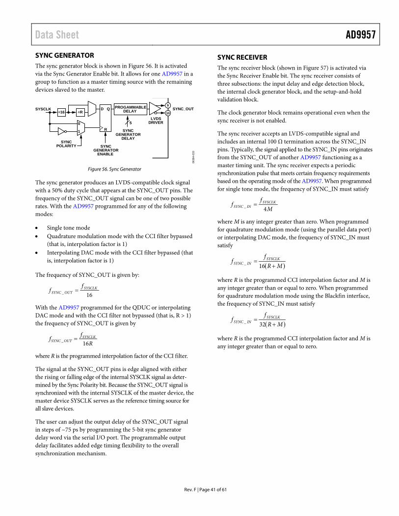
Data Sheet AD9957
Rev. F | Page 41 of 61
SYNC GENERATOR The sync generator block is shown in Figure 56. It is activated via the Sync Generator Enable bit. It allows for one AD9957 in a group to function as a master timing source with the remaining devices slaved to the master.
SYSCLK
SYNCGENERATOR
ENABLE
SYNCGENERATOR
DELAYSYNC
POLARITY
SYNC_OUT
0
1
D Q
R
PROGAMMABLEDELAY÷16 ÷R
5
9
10
LVDSDRIVER
0638
4-03
3
Figure 56. Sync Generator
The sync generator produces an LVDS-compatible clock signal with a 50% duty cycle that appears at the SYNC_OUT pins. The frequency of the SYNC_OUT signal can be one of two possible rates. With the AD9957 programmed for any of the following modes:
• Single tone mode • Quadrature modulation mode with the CCI filter bypassed
(that is, interpolation factor is 1) • Interpolating DAC mode with the CCI filter bypassed (that
is, interpolation factor is 1)
The frequency of SYNC_OUT is given by:
16_SYSCLK
OUTSYNCf
f =
With the AD9957 programmed for the QDUC or interpolating DAC mode and with the CCI filter not bypassed (that is, R > 1) the frequency of SYNC_OUT is given by
_ 16SYSCLK
SYNC OUTff
R=
where R is the programmed interpolation factor of the CCI filter.
The signal at the SYNC_OUT pins is edge aligned with either the rising or falling edge of the internal SYSCLK signal as deter-mined by the Sync Polarity bit. Because the SYNC_OUT signal is synchronized with the internal SYSCLK of the master device, the master device SYSCLK serves as the reference timing source for all slave devices.
The user can adjust the output delay of the SYNC_OUT signal in steps of ~75 ps by programming the 5-bit sync generator delay word via the serial I/O port. The programmable output delay facilitates added edge timing flexibility to the overall synchronization mechanism.
SYNC RECEIVER The sync receiver block (shown in Figure 57) is activated via the Sync Receiver Enable bit. The sync receiver consists of three subsections: the input delay and edge detection block, the internal clock generator block, and the setup-and-hold validation block.
The clock generator block remains operational even when the sync receiver is not enabled.
The sync receiver accepts an LVDS-compatible signal and includes an internal 100 Ω termination across the SYNC_IN pins. Typically, the signal applied to the SYNC_IN pins originates from the SYNC_OUT of another AD9957 functioning as a master timing unit. The sync receiver expects a periodic synchronization pulse that meets certain frequency requirements based on the operating mode of the AD9957. When programmed for single tone mode, the frequency of SYNC_IN must satisfy
Mf
f SYSCLKINSYNC 4_ =
where M is any integer greater than zero. When programmed for quadrature modulation mode (using the parallel data port) or interpolating DAC mode, the frequency of SYNC_IN must satisfy
( )MRf
f SYSCLKINSYNC +
=16_
where R is the programmed CCI interpolation factor and M is any integer greater than or equal to zero. When programmed for quadrature modulation mode using the Blackfin interface, the frequency of SYNC_IN must satisfy
( )MRf
f SYSCLKINSYNC +
=32_
where R is the programmed CCI interpolation factor and M is any integer greater than or equal to zero.

AD9957 Data Sheet
Rev. F | Page 42 of 61
LVDSRECEIVER
PROGAMMABLEDELAY
5INTERNALCLOCKS
CLOCKSTATE
6
SYNC STATEPRESET VALUE
SYNC PULSE
SYSCLKSETUP AND HOLD
VALIDATION
4
Q0
LOADQN
DELAYED SYNC-IN SIGNAL
SYNCRECEIVER
DELAY
SYNCRECEIVERENABLE
SYNC_SMP_ERR
SYNC_IN+
SYNC_IN–
7
8
12
RISING EDGEDETECTOR
ANDSTROBE
GENERATOR
SYNCTIMING
VALIDATIONDISABLE
SYNCVALIDATIONDELAY
0638
4-03
4
CLOCKGENERATOR
PRESET
......
Figure 57. Sync Receiver
When a device other than another AD9957 provides the SYNC_IN signal it must be LVDS compatible. Furthermore, although SYNC_IN is typically considered a periodic clock signal, it is not an absolute requirement. It is feasible to drive the SYNC_IN pins with a single synchronization pulse as long as its edge transition meets the setup/hold timing required for the internally generated sync pulse (as detailed later in this section). However, using a periodic SYNC_IN signal has the distinct advantage that should any of the devices arbitrarily lose synchronization it automatically resynchronizes with the arrival of the next SYNC_IN edge.
The 5-bit sync receiver delay word in the multichip sync register delays the SYNC_IN signal in steps of ~75 ps. This provides the ability to time align the arrival of the SYNC_IN signal to multiple devices by compensating for unequal propagation times.
The edge detection logic in the sync receiver generates a synchronization pulse (sync pulse) having a duration of one SYSCLK cycle with a repetition rate equal to that of the signal applied to the SYNC_IN pins. To produce the sync pulse, the strobe generator samples the delayed rising edge of the SYNC_IN signal with the rising edge of the local SYSCLK. The generation of this sync pulse is crucial to the operation of the synchroniza-tion mechanism, because it performs the task of placing the clock generator into a known state. The sync pulse presets the R-divider stage of the internal clock generator, which behaves as a presettable downcounter (see Figure 55). The programmable 6-bit sync state preset value word in the multichip sync register establishes the preset state. The preset state is only active for a single SYSCLK period, after which the clock generator is free to cycle through its state sequence until the next sync pulse arrives (see Figure 55). In addition to presetting the R-divider, the sync pulse also synchronously presets the other dividers to a proper state in order to preserve the cadence of the clock tree.
The ability to program the clock state preset value provides the flexibility to synchronize devices, but with specific relative clock state offsets by assigning a different sync state preset value word to each device in a group. This flexibility is limited, however, because the sync state preset value must adhere to certain bounds to satisfy internal timing requirements. Regardless of the programmed sync state preset value, the preset value is internally constrained to the range, 2 to R, where R is the CCI filter interpolation factor. A programmed value of 0 or 1 is forced to 2, whereas a programmed value greater than R is forced to R.
SETUP/HOLD VALIDATION Synchronization of the AD9957 internal clock generator with other external devices relies on the ability of the sync receiver’s edge detection circuit to generate a valid sync pulse. This requires proper sampling of the rising edge of the delayed SYNC_IN signal with the rising edge of the local SYSCLK. If the edge timing of these signals fails to meet the setup or hold time requirements of the internal latches in the edge detection circuitry, the proper generation of a sync pulse is in jeopardy. The setup-and-hold validation block (see Figure 58) gives the user a means to validate that proper edge timing exists between the two signals. The Sync Timing Validation Disable bit in Control Function Register 2 controls whether or not the setup-and-hold validation block is active.
The validation block makes use of a specified time window (programmable in increments of ~75 ps via the 4-bit sync validation delay word in the multichip sync register). The setup validation and hold validation circuits use latches identical to those in both the rising edge detector and strobe generator. The programmable time window skews the timing between the local SYSCLK signal and the delayed sync-in signal. If the hold valida-tion and setup validation circuits fail to produce the same logic states, it is an indication of a possible setup or hold violation. The check logic of Figure 58 monitors the state of the setup and hold validation latches. If they are not equal (that is, a potential setup/hold violation exists), a Logic 1 is stored in an internal
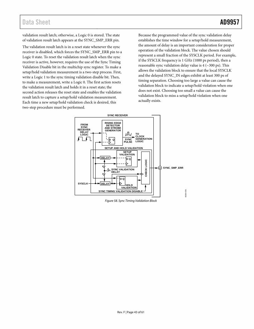
Data Sheet AD9957
Rev. F | Page 43 of 61
validation result latch; otherwise, a Logic 0 is stored. The state of validation result latch appears at the SYNC_SMP_ERR pin.
The validation result latch is in a reset state whenever the sync receiver is disabled, which forces the SYNC_SMP_ERR pin to a Logic 0 state. To reset the validation result latch when the sync receiver is active, however, requires the use of the Sync Timing Validation Disable bit in the multichip sync register. To make a setup/hold validation measurement is a two-step process. First, write a Logic 1 to the sync timing validation disable bit. Then, to make a measurement, write a Logic 0. The first action resets the validation result latch and holds it in a reset state; the second action releases the reset state and enables the validation result latch to capture a setup/hold validation measurement. Each time a new setup/hold validation check is desired, this two-step procedure must be performed.
Because the programmed value of the sync validation delay establishes the time window for a setup/hold measurement, the amount of delay is an important consideration for proper operation of the validation block. The value chosen should represent a small fraction of the SYSCLK period. For example, if the SYSCLK frequency is 1 GHz (1000 ps period), then a reasonable sync validation delay value is 4 (~300 ps). This allows the validation block to ensure that the local SYSCLK and the delayed SYNC_IN edges exhibit at least 300 ps of timing separation. Choosing too large a value can cause the validation block to indicate a setup/hold violation when one does not exist. Choosing too small a value can cause the validation block to miss a setup/hold violation when one actually exists.
SYNCPULSE
SYSCLK DELAY
CH
ECK
LO
GIC
4
4
SYNC VALIDATIONDELAY
SYNC_SMP_ERR
SYNC RECEIVER
SYNC TIMING VALIDATION DISABLE
SETUPVALIDATION
HOLDVALIDATION
12
SETUP AND HOLD VALIDATION
TOCLOCKGENERATIONLOGIC
FROMSYNC
RECEIVERDELAYLOGIC
D Q
D Q
D QDELAY
RISING EDGEDETECTOR
AND STROBEGENERATOR
0638
4-03
6
4
Figure 58. Sync Timing Validation Block

AD9957 Data Sheet
Rev. F | Page 44 of 61
SYNCHRONIZATION EXAMPLE To accomplish the synchronization of multiple devices provide each AD9957 with a SYNC_IN signal that is edge aligned across all the devices. If the SYNC_IN signal is edge aligned at all devices, and all devices have the same sync receiver delay and sync state preset value, then they all have matching clock states (that is, they are synchronized). Figure 59 shows this concept with three AD9957s in synchronization. One device operates as a master timing unit with the others synchronized to the master.
The master device must have its SYNC_IN pins included as part of the synchronization distribution and delay equalization mecha-nism. This ensures that the master maintains synchronous timing with the other units.
The synchronization mechanism begins with the clock distribu-tion and delay equalization block, which ensures that all devices receive an edge-aligned REFCLK signal. However, even though the REFCLK signal is edge aligned among all devices, this alone does not guarantee that the clock state of each internal clock
generator is coordinated with the others. This is the role of the synchronization and delay equalization block. This block accepts the SYNC_OUT signal generated by the master device and redistributes it to the SYNC_IN input of the slave units (as well as feeding it back to the master). The goal of the redistributed SYNC_OUT signal from the master device is to deliver an edge-aligned SYNC_IN signal to all of the sync receivers.
Assuming that all devices share the same REFCLK edge timing (due to the clock distribution and delay equalization block) and that all devices share the same SYNC_IN edge timing (due to the synchronization and delay equalization block), then all devices should be generating an internal sync pulse in unison (assuming all have the same value for the sync receiver delay). With the further stipulation that all devices have the same sync state preset value, then the synchronized sync pulses cause all of the devices to assume the same predefined clock state simultane-ously. That is, all devices have their internal clocks fully synchronized.
CLOCKSOURCE
SYNCIN
SYNCOUT
REF_CLK
AD9957NUMBER 1 MASTER DEVICEFPGA
DATA
FPGA
DATA
FPGA
DATA
EDGEALIGNED
AT REF_CLKINPUTS
EDGEALIGNED
AT SYNC_ININPUTS.
PD
CL
K
SYNCIN
SYNCOUT
REF_CLK
AD9957NUMBER 2
PD
CL
K
SYNCIN
SYNCOUT
REF_CLK
AD9957NUMBER 3
PD
CL
K
(FOR EXAMPLE, AD951x)
CLOCK DISTRIBUTIONAND
DELAY EQUALIZATION
SYNCHRONIZATIONDISTRIBUTION AND
DELAY EQUALIZATION(FOR EXAMPLE AD951x)
0638
4-03
5
Figure 59. Multichip Synchronization Example

Data Sheet AD9957
Rev. F | Page 45 of 61
I/Q PATH LATENCY The I/Q latency through the AD9957 is easiest to describe in terms of system clock (SYSCLK) cycles and is a function of the AD9957 configuration (that is, which mode and which optional features are engaged). The I/Q latency is primarily affected by the programmable CCI rate.
The values in Table 12 should be considered estimates because observed latency may be data dependent. The latency was calculated using the linear delay model for FIR filters. N = CCI rate (programmable interpolation rate, 2 to 63, 1 if bypassed).
In BFI mode, the latency through the AD9957 may not be con-stant for multiple transmissions. This is due to the relationship between the phase of the clock that drives the first half-band filter and the frame sync signal coming from the Blackfin, which is unknown and denoted as x in Table 12. The design successfully transfers data from the data assembler logic to the
signal process path by updating a parallel register at the proper time. The data is transferred from the parallel register to the signal processing chain and all timing has been verified regard-less of the phase relationship between the updating of the parallel register and the signal processing clock.
Example
Quadrature modulation mode = 18-bit parallel data Reference clock multiplier = bypassed Input scale multiplier = off Inverse CCI = off CCI rate = 20 Inverse SINC = on Output scale = off
Latency = (16 × 20) + (4 × 20) + (4 × 20) + (69 × 20) + (4 × 20 + 8) + 22 + 8 + 2 + 8 = 1988 SYSCLKs
Table 12. Stage Quadrature Modulation Mode—Parallel Quadrature Modulation Mode—BFI Interpolation DAC Mode Input Demuxplexer 16N (16 + x)N, where x = 0 to 15 28N Input Scale Multiplier Active: 8N Not available in BFI mode Active: 8N Bypassed: 4N Bypassed: 4N Inverse CCI Filter Active: 8N Active: 8N Active: 8N Bypassed: 4N Bypassed: 4N Bypassed: 4N Half-Band Filters 69N 345N 69N CCI Filter Active: 4N + 8 Active: 4N + 8 Active: 4N + 8 Bypass: 2N + 4 Bypass: 2N + 4 Bypass: 2N + 4 Modulator 22 22 0 Inverse Sinc Filter Active: 8 Active: 8 Active: 8 Bypass: 2 Bypass: 2 Bypass: 2 Output Scale Multiplier Active: 12 Active: 12 Active: 12 Bypass: 2 Bypass: 2 Bypass: 2 DAC Interface 8 8 8

AD9957 Data Sheet
Rev. F | Page 46 of 61
POWER SUPPLY PARTITIONING The AD9957 features multiple power supplies, and their power consumption varies with its configuration. This section covers which power supplies can be grouped together and how the power consumption of each block varies with frequency.
The values quoted in this section are for comparison only. Refer to Table 1 for exact values. With each group, bypass capacitors of 1 µF in parallel with a 10 µF capacitor should be used.
The recommendations here are for typical applications, for which there are four groups of power supplies: 3.3 V digital, 3.3 V analog, 1.8 V digital, and 1.8 V analog.
Applications demanding the highest performance may require additional power supply isolation.
3.3 V SUPPLIES DVDD_I/O (Pin 11, Pin 15, Pin 21, Pin 28, Pin 45, Pin 56, Pin 66)
These 3.3 V supplies can be grouped together. The power consumption on these pins varies dynamically with serial port activity.
AVDD (Pin 74 to Pin 77 and Pin 83)
These are 3.3 V DAC power supplies that typically consume about 28 mA. At a minimum, a ferrite bead should be used to isolate these from other 3.3 V supplies, with a separate regulator being ideal. The current consumption of these supplies consist mainly of biasing current and do not vary with frequency.
1.8 V SUPPLIES DVDD (Pin 17, Pin 23, Pin 30, Pin 47, Pin 57, Pin 64)
These pins can be grouped together. Their current consumption increases linearly with the system clock frequency. A system clock of 1 GHz produces a typically current consumption of 610 mA in QDUC mode. There is also a slight (~5%) increase as fOUT increases from 50 MHz to 400 MHz.
AVDD (Pin 3)
This 1.8 V supply powers the REFCLK multiplier (PLL) and consumes about 7 mA. For applications demanding the highest performance with the PLL enabled, this supply should be isolated from other 1.8 V AVDD supplies with a separate regulator. For less demanding applications, this supply can be run off the same regulator as Pin 89, Pin 92 with a ferrite bead to isolate Pin 3 from Pin 89, and Pin 89.
The loop filter for the PLL should directly connect to Pin 3. If the PLL is bypassed, pin 3 should still be powered, but isolation is not critical.
AVDD (Pin 6)
This pin can be grouped together with the DVDD 1.8V supply pins. For the highest performance, a ferrite bead should be used for isolation, with a separate regulator being ideal.
AVDD (Pin 89 and Pin 92)
This 1.8 V supply for the REFCLK input consumes about 15 mA. The supply can be run off the same as Pin 3 with a ferrite bead to isolate Pin 3 from Pin 89 and Pin 92. At a minimum, a ferrite bead should be used to isolate these from other 1.8 V supplies. However, for applications demanding the highest performance, a separate regulator is recommended.

Data Sheet AD9957
Rev. F | Page 47 of 61
SERIAL PROGRAMMING CONTROL INTERFACE—SERIAL I/O The AD9957 serial port is a flexible, synchronous serial commu-nications port allowing easy interface to many industry-standard microcontrollers and microprocessors.
The interface allows read/write access to all registers that configure the AD9957. MSB-first or LSB-first transfer formats are sup-ported. In addition, the serial interface port can be configured as a single pin input/output (SDIO) allowing a two-wire interface, or it can be configured as two unidirectional pins for input/output (SDIO/SDO), enabling a 3-wire interface. Two optional pins (I/O_RESET and CS) enable greater flexibility for designing systems with the AD9957.
GENERAL SERIAL I/O OPERATION There are two phases to a serial communications cycle. The first is the instruction phase to write the instruction byte into the AD9957. The instruction byte contains the address of the regis-ter to be accessed (see the Register Map and Bit Descriptions section) and defines whether the upcoming data transfer is a write or read operation.
For a write cycle, Phase 2 represents the data transfer between the serial port controller to the serial port buffer. The number of bytes transferred is a function of the register being accessed. For example, when accessing the Control Function Register 2 (Address 0x01), Phase 2 requires that four bytes be transferred. Each bit of data is registered on each corresponding rising edge of SCLK. The serial port controller expects that all bytes of the register be accessed; otherwise, the serial port controller is put out of sequence for the next communication cycle. However, one way to write fewer bytes than required is to use the I/O_RESET pin feature. The I/O_RESET pin function can be used to abort an I/O operation and reset the pointer of the serial port con-troller. After an I/O reset, the next byte is the instruction byte. Note that every completed byte written prior to an I/O reset is preserved in the serial port buffer. Partial bytes written are not preserved. At the completion of any communication cycle, the AD9957 serial port controller expects the next eight rising SCLK edges to be the instruction byte for the next communi-cation cycle.
After a write cycle, the programmed data resides in the serial port buffer and is inactive. I/O_UPDATE transfers data from the serial port buffer to active registers. The I/O update can either be sent after each communication cycle or when all serial operations are complete. In addition, a change in profile pins can initiate an I/O update.
For a read cycle, Phase 2 is the same as the write cycle with the following differences: Data is read from the active registers, not the serial port buffer, and data is driven out on the falling edge of SCLK.
Note that to read back any profile register (0x0E to 0x15), the three external profile pins must be used. For example, if the profile register is Profile 5 (0x13) then PROFILE0 to PROFILE2 pins must equal 101.This is not required to write to profile registers.
INSTRUCTION BYTE The instruction byte contains the following information as shown in the instruction byte bit map.
Instruction Byte Information Bit Map
MSB LSB D7 D6 D5 D4 D3 D2 D1 D0 R/W X X A4 A3 A2 A1 A0
R/W—Bit 7 of the instruction byte determines whether a read or write data transfer occurs after the instruction byte write. Logic 1 indicates a read operation. Cleared indicates a write operation.
X, X—Bit 6 and Bit 5 of the instruction byte are don’t cares.
A4, A3, A2, A1, A0—Bit 4, Bit 3, Bit 2, Bit 1, and Bit 0 of the instruction byte determine which register is accessed during the data transfer portion of the communications cycle.
SERIAL I/O PORT PIN DESCRIPTIONS SCLK—Serial Clock
The serial clock pin is used to synchronize data to and from the AD9957 and to run the internal state machines.
CS—Chip Select Bar
An active low input that allows more than one device on the same serial communications line. The SDO and SDIO pins go to a high impedance state when this input is high. If driven high during any communications cycle, that cycle is suspended until CS is reactivated low. Chip select (CS) can be tied low in systems that maintain control of SCLK.
SDIO—Serial Data Input/Output
Data is always written into the AD9957 on this pin. However, this pin can be used as a bidirectional data line. Bit 1 of CFR1, Register Address 0x00, controls the configuration of this pin. The default is cleared, which configures the SDIO pin as bidirectional.

AD9957 Data Sheet
Rev. F | Page 48 of 61
SDO—Serial Data Out
Data is read from this pin for protocols that use separate lines for transmitting and receiving data. In the case where the AD9957 operates in a single bidirectional I/O mode, this pin does not output data and is set to a high impedance state.
I/O_RESET—Input/Output Reset
I/O_RESET synchronizes the I/O port state machines without affecting the addressable registers contents. An active high input on the I/O_RESET pin causes the current communication cycle to abort. After I/O_RESET returns low (Logic 0), another communication cycle can begin, starting with the instruction byte write.
I/O_UPDATE—Input/Output Update
The I/O_UPDATE initiates the transfer of written data from the I/O port buffer to active registers. I/O_UPDATE is active on the rising edge and its pulse width must be greater than one SYNC_CLK period. It is either an input or output pin depending on the programming of the Internal I/O Update Active bit.
SERIAL I/O TIMING DIAGRAMS Figure 60 through Figure 63 provide basic examples of the tim-ing relationships between the various control signals of the serial I/O port. Most of the bits in the register map are not transferred to their internal destinations until assertion of an I/O update, which is not included in the timing diagrams that follow.
MSB/LSB TRANSFERS The AD9957 serial port can support both most significant bit (MSB) first or least significant bit (LSB) first data formats. This functionality is controlled by Bit 0 in Control Function Register 1 (0x00). The default format is MSB first. If LSB first is active, all data, including the instruction byte, must follow LSB-first convention. Note that the highest number found in the bit range column for each register is the MSB and the lowest number is the LSB for that register (see the Register Map and Bit Descriptions section and Table 13).
0638
4-03
7
I7SDIO
INSTRUCTION CYCLE DATA TRANSFER CYCLE
SCLK
CS
I6 I5 I4 I3 I2 I1 I0 D7 D6 D5 D4 D3 D2 D1 D0
Figure 60. Serial Port Write Timing—Clock Stall Low
0638
4-03
8
DO7
INSTRUCTION CYCLE DATA TRANSFER CYCLE
DON'T CAREI7 I6 I5 I4 I3 I2 I1 I0SDIO
SCLK
CS
SDO DO6 DO5 DO4 DO3 DO2 DO1 DO0
Figure 61. 3-Wire Serial Port Read Timing—Clock Stall Low
0638
4-03
9
I7SDIO
INSTRUCTION CYCLE DATA TRANSFER CYCLE
SCLK
CS
I6 I5 I4 I3 I2 I1 I0 D7 D6 D5 D4 D3 D2 D1 D0
Figure 62. Serial Port Write Timing—Clock Stall High
0638
4-04
0
I7SDIO
INSTRUCTION CYCLE DATA TRANSFER CYCLE
SCLK
CS
I6 I5 I4 I3 I2 I1 I0 DO7 DO6 DO5 DO4 DO3 DO2 DO1 DO0
Figure 63. 2-Wire Serial Port Read Timing—Clock Stall High

Data Sheet AD9957
Rev. F | Page 49 of 61
I/O_UPDATE, SYNC_CLK, AND SYSTEM CLOCK RELATIONSHIPS The I/O_UPDATE pin is used to transfer data from the serial I/O buffer to the active registers in the device. Data in the buffer is inactive.
SYNC_CLK is a rising edge active signal. It is derived from the system clock and a divide-by-4 frequency divider. SYNC_CLK, which is externally provided, can be used to synchronize external hardware to the AD9957 internal clocks.
I/O_UPDATE initiates the start of a buffer transfer. It can be sent synchronously or asynchronously relative to the SYNC_CLK. If the setup time between these signals is met, then constant latency (pipeline) to the DAC output exists. For example, if repetitive changes to phase offset via the SPI
port is desired, the latency of those changes to the DAC output is constant; otherwise, a time uncertainty of one SYNC_CLK period is present.
By default, the I/O_UPDATE pin is an input that serves as a strobe signal to allow synchronous update of the device oper-ating parameters. A rising edge on I/O_UPDATE initiates transfer of the register contents to the internal workings of the device. Alternatively, the transfer of programmed data from the programming registers to the internal hardware can be accomplished by changing the state of the PROFILE2, PROFILE1, and PROFILE0 pins.
The timing diagram shown in Figure 64 depicts when the data in the buffer is transferred to the active registers.
SYNC_CLK
SYSCLK
A B
N N + 1N – 1DATA INREGISTERS
DATA INI/O BUFFERS N N + 1 N + 2
I/O_UPDATE
THE DEVICE REGISTERS AN I/O UPDATE AT POINT A. THE DATA IS TRANSFERRED FROM THE ASYNCHRONOUSLY LOADED I/O BUFFERS AT POINT B. 0638
4-16
1
Figure 64. I/O_UPDATE Transferring Data from I/O Buffer to Active Registers

AD9957 Data Sheet
Rev. F | Page 50 of 61
REGISTER MAP AND BIT DESCRIPTIONS REGISTER MAP Note that the highest number found in the Bit Range column for each register in the following tables is the MSB and the lowest number is the LSB for that register.
Table 13. Control Registers Register Name (Serial Address)
Bit Range (Internal Address)
Bit 7 (MSB) Bit 6 Bit 5 Bit 4 Bit 3 Bit 2 Bit 1
Bit 0 (LSB)
Default Value
Control Function Register 1 CFR1 (0x00)
[31:24] RAM Enable
Open RAM Playback Destination
Open Operating Mode 0x00
[23:16] Manual OSK External Control
Inverse Sinc Filter Enable
Clear CCI Open Select DDS Sine Output
0x00
[15:8] Open Autoclear Phase Accumulator
Open Clear Phase Accumulator
Load ARR at I/O Update
OSK Enable
Select Auto-OSK
0x00
[7:0] Digital Power- Down
DAC Power- Down
REFCLK Input Power-Down
Aux DAC Power-Down
External Power-Down Control
Auto Power-Down Enable
SDIO Input Only
LSB First 0x00
Control Function Register 2 CFR2 (0x01)
[31:24] Blackfin Interface Mode Active
Blackfin Bit Order
Blackfin Early Frame Sync Enable
Open Enable Profile
Registers as ASF Source
0x00
[23:16] Internal I/O Update Active
SYNC_CLK Enable
Open Read Effective FTW
0x40
[15:8] I/O Update Rate Control PDCLK Rate Control
Data Format PDCLK Enable
PDCLK Invert
TxENABLE Invert
Q-First Data Pairing
0x08
[7:0] Open Data Assembler Hold Last Value
Sync Timing Validation Disable
Open 0x20
Control Function Register 3 CFR3 (0x02)
[31:24] Open DRV0[1:0] Open VCO SEL[2:0] 0x1F
[23:16] Open ICP[2:0] Open 0x3F [15:8] REFCLK
Input Divider Bypass
REFCLK Input Divider ResetB
Open PLL Enable
0x40
[7:0] N[6:0] Open 0x00
Auxiliary DAC Control Register (0x03)
[31:24] Open 0x00
[23:16] Open 0x00
[15:8] Open 0x7F
[7:0] FSC[7:0] 0x7F
I/O Update Rate Register (0x04)
[31:24] I/O Update Rate[31:24] 0xFF
[23:16] I/O Update Rate[23:16] 0xFF
[15:8] I/O Update Rate[15:8] 0xFF
[7:0] I/O Update Rate[7:0] 0xFF

Data Sheet AD9957
Rev. F | Page 51 of 61
Table 14. RAM, ASF, Multichip Sync, and Profile 0 Registers
Register Name (Serial Address)
Bit Range (Internal Address)
Bit 7 (MSB) Bit 6 Bit5 Bit 4 Bit 3 Bit 2 Bit 1
Bit 0 (LSB)
Default Value
RAM Segment Register 0 (0x05)
[47:40] RAM Address Step Rate 0[15:8]
[39:32] RAM Address Step Rate 0[7:0]
[31:24] RAM End Address 0[9:2]
[23:16] RAM End Address 0[1:0]
Open
[15:8] RAM Start Address 0[9:2]
[7:0] RAM Start Address 0[1:0]
Open RAM Playback Mode 0[2:0]
RAM Segment Register 1 (0x06)
[47:40] RAM Address Step Rate 1[15:8]
[39:32] RAM Address Step Rate 1[7:0]
[31:24] RAM End Address 1[9:2] [23:16] RAM End
Address 1[1:0] Open
[15:8] RAM Start Address 1[9:2] [7:0] RAM Start
Address 1[1:0] Open RAM Playback Mode 1[2:0]
Amplitude Scale Factor (ASF) Register (0x09)
[31:24] Amplitude Ramp Rate[15:8] 0x00 [23:16] Amplitude Ramp Rate[7:0] 0x00
[15:8] Amplitude Scale Factor]13:6] 0x00
[7:0] Amplitude Scale Factor[5:0] Amplitude Step Size[1:0] 0x00
Multichip Sync Register (0x0A)
[1:24] Sync Validation Delay[3:0] Sync Receiver Enable
Sync Generator Enable
Sync Generator Polarity
Open 0x00
[23:16] Sync State Preset Value[5:0] Open 0x00
[15:8] Sync Generator Delay[4:0] Open 0x00
[7:0] Sync Receiver Delay[4:0] Open 0x00
Profile 0 Register—Single Tone (0x0E)
[63:56] Open Amplitude Scale Factor[13:8] 0x08
[55:48] Amplitude Scale Factor[7:0] 0xB5
[47:40] Phase Offset Word[15:8] 0x00
[39:32] Phase Offset Word[7:0] 0x00
[31:24] Frequency Tuning Word[31:24] 0x00
[23:16] Frequency Tuning Word[23:16] 0x00
[15:8] Frequency Tuning Word[15:8] 0x00
[7:0] Frequency Tuning Word[7:0] 0x00
Profile 0 Register—QDUC (0x0E)
[63:56] CCI Interpolation Rate[7:2] Spectral Invert Inverse CCI Bypass
0x00
[55:48] Output Scale Factor 0x00
[47:40] Phase Offset Word[15:8] 0x00
[39:32] Phase Offset Word[7:0] 0x00
[31:24] Frequency Tuning Word[31:24] 0x00
[23:16] Frequency Tuning Word[23:16] 0x00
[15:8] Frequency Tuning Word[15:8] 0x00
[7:0] Frequency Tuning Word[7:0] 0x00

AD9957 Data Sheet
Rev. F | Page 52 of 61
Table 15. Profile 1, Profile 2, and Profile 3 Registers Register Name (Serial Address)
Bit Range (Internal Address)
Bit 7 (MSB) Bit 6 Bit 5 Bit 4 Bit 3 Bit 2 Bit 1
Bit 0 (LSB)
Default Value
Profile 1 Register—Single Tone (0x0F)
[63:56] Open Amplitude Scale Factor[13:8] 0x00
[55:48] Amplitude Scale Factor[7:0] 0x00
[47:40] Phase Offset Word[15:8] 0x00 [39:32] Phase Offset Word[7:0] 0x00
[31:24] Frequency Tuning Word[31:24] 0x00
[23:16] Frequency Tuning Word[23:16] 0x00
[15:8] Frequency Tuning Word[15:8] 0x00
[7:0] Frequency Tuning Word[7:0] 0x00
Profile 1 Register—QDUC (0x0F)
[63:56] CCI Interpolation Rate[7:2] Spectral Invert
Inverse CCI Bypass
0x00
[55:48] Output Scale Factor[7:0] 0x00
[47:40] Phase Offset Word[15:8] 0x00
[39:32] Phase Offset Word[7:0] 0x00
[31:24] Frequency Tuning Word[31:24] 0x00
[23:16] Frequency Tuning Word[23:16] 0x00
[15:8] Frequency Tuning Word[15:8] 0x00
[7:0] Frequency Tuning Word[7:0] 0x00
Profile 2 Register— Single Tone (0x10)
[63:56] Open Amplitude Scale Factor[13:8] 0x00
[55:48] Amplitude Scale Factor[7:0] 0x00
[47:40] Phase Offset Word[15:8] 0x00
[39:32] Phase Offset Word[7:0] 0x00
[31:24] Frequency Tuning Word[31:24] 0x00
[23:16] Frequency Tuning Word[23:16] 0x00
[15:8] Frequency Tuning Word[15:8] 0x00
[7:0] Frequency Tuning Word[7:0] 0x00 Profile 2 Register—QDUC (0x10)
[63:56] CCI Interpolation Rate[7:2] Spectral Invert
Inverse CCI Bypass
0x00
[55:48] Output Scale Factor[7:0] 0x00 [47:40] Phase Offset Word[15:8] 0x00
[39:32] Phase Offset Word[7:0] 0x00
[31:24] Frequency Tuning Word[31:24] 0x00
[23:16] Frequency Tuning Word[23:16] 0x00
[15:8] Frequency Tuning Word[15:8] 0x00
[7:0] Frequency Tuning Word[7:0] 0x00
Profile 3 Register— Single Tone (0x11)
[63:56] Open Amplitude Scale Factor[13:8] 0x00
[55:48] Amplitude Scale Factor[7:0] 0x00
[47:40] Phase Offset Word[15:8] 0x00
[39:32] Phase Offset Word[7:0] 0x00
[31:24] Frequency Tuning Word[31:24] 0x00
[23:16] Frequency Tuning Word[23:16] 0x00
[15:8] Frequency Tuning Word[15:8] 0x00
[7:0] Frequency Tuning Word[7:0] 0x00
Profile 3 Register—QDUC (0x11)
[63:56] CCI Interpolation Rate[7:2] Spectral Invert
Inverse CCI Bypass
0x00
[55:48] Output Scale Factor[7:0] 0x00
[47:40] Phase Offset Word[15:8] 0x00
[39:32] Phase Offset Word[7:0] 0x00
[31:24] Frequency Tuning Word[31:24] 0x00
[23:16] Frequency Tuning Word[23:16] 0x00
[15:8] Frequency Tuning Word[15:8] 0x00 [7:0] Frequency Tuning Word[7:0] 0x00
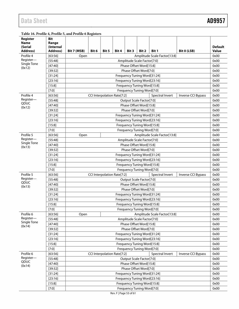
Data Sheet AD9957
Rev. F | Page 53 of 61
Table 16. Profile 4, Profile 5, and Profile 6 Registers Register Name (Serial Address)
Bit Range (Internal Address) Bit 7 (MSB) Bit 6 Bit 5 Bit 4 Bit 3 Bit 2 Bit 1 Bit 0 (LSB)
Default Value
Profile 4 Register— Single Tone (0x12)
[63:56] Open Amplitude Scale Factor[13:8] 0x00 [55:48] Amplitude Scale Factor[7:0] 0x00 [47:40] Phase Offset Word[15:8] 0x00 [39:32] Phase Offset Word[7:0] 0x00 [31:24] Frequency Tuning Word[31:24] 0x00 [23:16] Frequency Tuning Word[23:16] 0x00 [15:8] Frequency Tuning Word[15:8] 0x00 [7:0] Frequency Tuning Word[7:0] 0x00
Profile 4 Register— QDUC (0x12)
[63:56] CCI Interpolation Rate[7:2] Spectral Invert Inverse CCI Bypass 0x00 [55:48] Output Scale Factor[7:0] 0x00 [47:40] Phase Offset Word[15:8] 0x00 [39:32] Phase Offset Word[7:0] 0x00 [31:24] Frequency Tuning Word[31:24] 0x00 [23:16] Frequency Tuning Word[23:16] 0x00 [15:8] Frequency Tuning Word[15:8] 0x00 [7:0] Frequency Tuning Word[7:0] 0x00
Profile 5 Register— Single Tone (0x13)
[63:56] Open Amplitude Scale Factor[13:8] 0x00 [55:48] Amplitude Scale Factor[7:0] 0x00 [47:40] Phase Offset Word[15:8] 0x00 [39:32] Phase Offset Word[7:0] 0x00 [31:24] Frequency Tuning Word[31:24] 0x00 [23:16] Frequency Tuning Word[23:16] 0x00 [15:8] Frequency Tuning Word[15:8] 0x00 [7:0] Frequency Tuning Word[7:0] 0x00
Profile 5 Register— QDUC (0x13)
[63:56] CCI Interpolation Rate[7:2] Spectral Invert Inverse CCI Bypass 0x00 [55:48] Output Scale Factor[7:0] 0x00 [47:40] Phase Offset Word[15:8] 0x00 [39:32] Phase Offset Word[7:0] 0x00 [31:24] Frequency Tuning Word[31:24] 0x00 [23:16] Frequency Tuning Word[23:16] 0x00 [15:8] Frequency Tuning Word[15:8] 0x00 [7:0] Frequency Tuning Word[7:0] 0x00
Profile 6 Register— Single Tone (0x14)
[63:56] Open Amplitude Scale Factor[13:8] 0x00 [55:48] Amplitude Scale Factor[7:0] 0x00 [47:40] Phase Offset Word[15:8] 0x00 [39:32] Phase Offset Word[7:0] 0x00 [31:24] Frequency Tuning Word[31:24] 0x00 [23:16] Frequency Tuning Word[23:16] 0x00 [15:8] Frequency Tuning Word[15:8] 0x00 [7:0] Frequency Tuning Word[7:0] 0x00
Profile 6 Register— QDUC (0x14)
[63:56] CCI Interpolation Rate[7:2] Spectral Invert Inverse CCI Bypass 0x00 [55:48] Output Scale Factor[7:0] 0x00 [47:40] Phase Offset Word[15:8] 0x00 [39:32] Phase Offset Word[7:0] 0x00 [31:24] Frequency Tuning Word[31:24] 0x00 [23:16] Frequency Tuning Word[23:16] 0x00 [15:8] Frequency Tuning Word[15:8] 0x00 [7:0] Frequency Tuning Word[7:0] 0x00
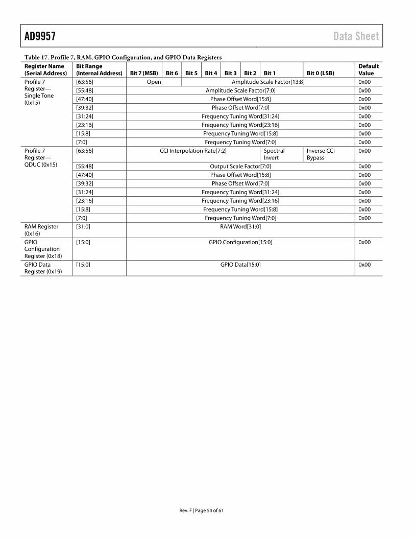
AD9957 Data Sheet
Rev. F | Page 54 of 61
Table 17. Profile 7, RAM, GPIO Configuration, and GPIO Data Registers Register Name (Serial Address)
Bit Range (Internal Address) Bit 7 (MSB) Bit 6 Bit 5 Bit 4 Bit 3 Bit 2 Bit 1 Bit 0 (LSB)
Default Value
Profile 7 Register— Single Tone (0x15)
[63:56] Open Amplitude Scale Factor[13:8] 0x00 [55:48] Amplitude Scale Factor[7:0] 0x00 [47:40] Phase Offset Word[15:8] 0x00 [39:32] Phase Offset Word[7:0] 0x00 [31:24] Frequency Tuning Word[31:24] 0x00 [23:16] Frequency Tuning Word[23:16] 0x00 [15:8] Frequency Tuning Word[15:8] 0x00 [7:0] Frequency Tuning Word[7:0] 0x00
Profile 7 Register— QDUC (0x15)
[63:56] CCI Interpolation Rate[7:2] Spectral Invert
Inverse CCI Bypass
0x00
[55:48] Output Scale Factor[7:0] 0x00 [47:40] Phase Offset Word[15:8] 0x00 [39:32] Phase Offset Word[7:0] 0x00 [31:24] Frequency Tuning Word[31:24] 0x00 [23:16] Frequency Tuning Word[23:16] 0x00 [15:8] Frequency Tuning Word[15:8] 0x00 [7:0] Frequency Tuning Word[7:0] 0x00
RAM Register (0x16)
[31:0] RAM Word[31:0]
GPIO Configuration Register (0x18)
[15:0] GPIO Configuration[15:0] 0x00
GPIO Data Register (0x19)
[15:0] GPIO Data[15:0] 0x00

Data Sheet AD9957
Rev. F | Page 55 of 61
REGISTER BIT DESCRIPTIONS The serial I/O port registers span an address range of 0 to 25 (0x00 to 0x19 in hexadecimal notation). This represents a total of 26 registers. However, six of these registers are unused, yielding a total of 20 available registers. The unused registers are 7, 8, 11 to 13, and 23 (0x07 to 0x08, 0x0B to 0x0D, and 0x17).
The number of bytes assigned to the registers varies. That is, the registers are not of uniform depth; each contains the number of bytes necessary for its particular function. Additionally, the registers are assigned names according to their functionality. In some cases, a register is given a mnemonic descriptor. For example, the register at Serial Address 0x00 is named Control Function Register 1 and is assigned the mnemonic CFR1.
The following section provides a detailed description of each bit in the AD9957 register map. For cases in which a group of bits serves a specific function, the entire group is considered as a binary word and described in aggregate.
This section is organized in sequential order of the serial addresses of the registers. Following each subheading are the individual bit descriptions for that particular register. The location of the bit(s) in the register are indicated by [A] or [A:B], where A and B are bit numbers. The notation, [A:B], specifies a range of bits from most significant to least significant bit position. For example, [5:2] means bit positions 5 down to 2, inclusive, with Bit 0 identifying the LSB of the register.
Unless otherwise stated, programmed bits are not transferred to their internal destinations until the assertion of an I/O update or profile change.
Control Function Register 1 (CFR1)
Address 0x00, four bytes are assigned to this register.
Table 18. Bit Descriptions for CFR1 Register Bit (s) Mnemonic Description 31 RAM Enable 0: disables RAM playback functionality (default).
1: enables RAM playback functionality. [30:29] Open 28 RAM Playback
Destination Ineffective unless CFR1, Bit 31 = 1. 0: RAM playback data routed to baseband scaling multipliers (default). 1: RAM playback data routed to baseband I/Q data path.
[27:26] Open [25:24] Operating Mode 00: quadrature modulation mode (default).
01: single tone mode. 1x: interpolating DAC mode.
23 Manual OSK External Control
Ineffective unless CFR1[9:8] = 10b. 0: OSK pin inoperative (default). 1: OSK pin enabled for manual OSK control (see the Output Shift Keying (OSK) section).
22 Inverse Sinc Filter Enable
0: inverse sinc filter bypassed (default). 1: inverse sinc filter active.
21 Clear CCI The serial I/O port controller automatically clears this bit. This operation requires several internal clock cycles to complete, during which time the data supplied to the CCI input by the baseband signal chain is ignored. The inputs are forced to all zeros to flush the CCI data path, after which the CCI accumulators are reset. 0: normal operation of the CCI filter (default). 1: initiates an asynchronous reset of the accumulators in the CCI filter.
[20:17] Open 16 Select DDS Sine
Output Ineffective unless CFR1[25:24] = 01b. 0: cosine output of the DDS is selected (default). 1: sine output of the DDS is selected.
[15:14] Open 13 Autoclear Phase
Accumulator 0: normal operation of the DDS phase accumulator (default). 1: synchronously resets the DDS phase accumulator any time I/O_UPDATE is asserted or a profile change occurs.
12 Open 11 Clear Phase
Accumulator 0: normal operation of the DDS phase accumulator (default). 1: asynchronous, static reset of the DDS phase accumulator.
10 Load ARR at I/O Update
0: normal operation of the OSK amplitude ramp rate timer (default). 1: OSK amplitude ramp rate timer reloaded any time I/O_UPDATE is asserted or a profile change occurs.

AD9957 Data Sheet
Rev. F | Page 56 of 61
Bit (s) Mnemonic Description 9 OSK (Output Shift
Keying) Enable 0: OSK disabled (default). 1: OSK enabled.
8 Select Auto-OSK Ineffective unless CFR1, Bit 9 = 1. 0: manual OSK enabled (default). 1: automatic OSK enabled.
7 Digital Power-Down
This bit is effective without the need for an I/O update. 0: clock signals to the digital core are active (default). 1: clock signals to the digital core are disabled.
6 DAC Power-Down 0: DAC clock signals and bias circuits are active (default). 1: DAC clock signals and bias circuits are disabled.
5 REFCLK Input Power-Down
This bit is effective without the need for an I/O update. 0: REFCLK input circuits and PLL are active (default). 1: REFCLK input circuits and PLL are disabled.
4 Auxiliary DAC Power-Down
0: auxiliary DAC clock signals and bias circuits are active (default). 1: auxiliary DAC clock signals and bias circuits are disabled.
3 External Power-Down Control
0: assertion of the EXT_PWR_DWN pin affects full power-down (default). 1: assertion of the EXT_PWR_DWN pin affects fast recovery power-down.
2 Auto Power-Down Enable
Ineffective when CFR1[25:24] = 01b. 0: disable power-down (default). 1: when the TxENABLE pin is Logic 0, the baseband signal processing chain is flushed of residual data and the clocks are automatically stopped. Clocks restart when the TxENABLE pin is a Logic 1.
1 SDIO Input Only 0: configures the SDIO pin for bidirectional operation; 2-wire serial programming mode (default). 1: configures the serial data I/O pin (SDIO) as an input only pin; 3-wire serial programming mode.
0 LSB First 0: configures the serial I/O port for MSB first format (default). 1: configures the serial I/O port for LSB first format.
Control Function Register 2 (CFR2)
Address 0x01, four bytes are assigned to this register.
Table 19. Bit Descriptions for CFR2 Register Bit (s) Mnemonic Description 31 Blackfin Interface Mode Active Valid only when CFR1[25:24] = 00b (quadrature modulation mode).
0: Pin D[17:0] configured as an 18-bit parallel port (default). 1: Pin D[5:4] configured as a dual serial port compatible with the Blackfin serial interface. Pin D[17:6] and Pin D[3:0] become available as a 16-bit GPIO port.
30 Blackfin Bit Order Valid only when CFR2, Bit 31 = 1. 0: the dual serial port (BFI) configured for MSB first operation (default). 1: the dual serial port (BFI) configured for LSB first operation.
29 Blackfin Early Frame Sync Enable Valid only when CFR2, Bit 31 = 1. 0: the dual serial port (BFI) configured to be compatible with Blackfin late frame sync operation (default). 1: the dual serial port (BFI) configured to be compatible with Blackfin early frame sync operation.
[28:25] Open 24 Enable Profile Registers as ASF Source Valid only when CFR1[25:24] = 01b (single tone mode) and CFR1, Bit 9 = 0 (OSK disabled).
0: amplitude scale factor bypassed (unity gain). 1: the active profile register determines the amplitude scale factor.
23 Internal I/O Update Active This bit is effective without the need for an I/O update. 0: serial I/O programming is synchronized with external assertion of the I/O_UPDATE pin, which is configured as an input pin (default). 1: serial I/O programming is synchronized with an internally generated I/O update signal (the internally generated signal appears at the I/O_UPDATE pin, which is configured as an output pin).

Data Sheet AD9957
Rev. F | Page 57 of 61
Bit (s) Mnemonic Description 22 SYNC_CLK Enable 0: the SYNC_CLK pin is disabled; static Logic 0 output.
1: the SYNC_CLK pin generates a clock signal at ¼ fSYSCLK; use of synchronization of the serial I/O port (default).
[21:17] Open 16 Read Effective FTW 0: a serial I/O port read operation of the FTW register reports the contents of the FTW
register (default). 1: a serial I/O port read operation of the FTW register reports the actual 32-bit word appearing at the input to the DDS phase accumulator.
[15:14] I/O Update Rate Control Ineffective unless CFR2, Bit 23 = 1. Sets the prescale ratio of the divider that clocks the I/O update timer as follows: 00: divide by 1 (default). 01: divide by 2. 10: divide by 4. 11: divide by 8.
13 PDCLK Rate Control Ineffective unless CFR2, Bit 31 = 0 and CFR1[25:24] = 00b. 0: PDCLK operates at the input data rate (default). 1: PDCLK operates at ½ the input data rate; useful for maintaining a consistent relationship between I/Q words at the parallel data port and the internal clocks of the baseband signal processing chain.
12 Data Format 0: the data-words applied to Pin D[17:0] are expected to be coded as twos complement (default). 1: the data-words applied to Pin D[17:0] are expected to be coded as offset binary.
11 PDCLK Enable 0: the PDCLK pin is disabled and forced to a static Logic 0 state; the internal clock signal continues to operate and provide timing to the data assembler. 1: the internal PDCLK signal appears at the PDCLK pin (default).
10 PDCLK Invert 0: normal PDCLK polarity; Q-data associated with Logic 1, I-data with Logic 0 (default). 1: inverted PDCLK polarity.
9 TxENABLE Invert 0: normal TxENABLE polarity; Logic 0 is standby, Logic 1 is transmit (default). 1: inverted TxENABLE polarity; Logic 0 is transmit, Logic 1 is standby.
8 Q-First Data Pairing 0: an I/Q data pair is delivered as I-data first, followed by Q-data (default). 1: an I/Q data pair is delivered as Q-data first, followed by I-data.
7 Open 6 Data Assembler Hold Last Value Ineffective when CFR1[25:24] = 01b.
0: when the TxENABLE pin is false, the data assembler ignores the input data and internally forces zeros on the baseband signal path (default). 1: when the TxENABLE pin is false, the data assembler ignores the input data and internally forces the last value received on the baseband signal path.
5 Sync Timing Validation Disable 0: enables the setup and hold validation circuit to take a measurement; the measurement result appears at the SYNC_SMP_ERR pin; a Logic 1 at this pin indicates a potential setup/hold violation whereas a Logic 0 indicates that a setup/hold violation has not been detected; the measurement result is latched and held until this bit is set to a Logic 1. 1: resets the setup and hold validation measurement circuit forcing the SYNC_SMP_ERR pin to a static Logic 0 condition (default); the measurement circuit is effectively disabled until this bit is restored to a Logic 0 state.
[4:0] Open

AD9957 Data Sheet
Rev. F | Page 58 of 61
Control Function Register 3 (CFR3) Address 0x02, four bytes are assigned to this register.
Table 20. Bit Descriptions for CFR3 Register Bit (s) Mnemonic Description [31:30] Open [29:28] DRV0 Controls REFCLK_OUT pin (see Table 6 for details); default is 01b. 27 Open [26:24] VCO SEL Selects frequency band of the VCO in the REFCLK PLL (see Table 7 for details); default is 111b. [23:22] Open [21:19] ICP Selects the charge pump current in the REFCLK PLL (see Table 8 for details); default is 111b. [18:16] Open 15 REFCLK Input Divider Bypass 0: input divider is selected (default).
1: input divider is bypassed. 14 REFCLK Input Divider ResetB 0: input divider is reset.
1: input divider operates normally (default). [13:9] Open 8 PLL Enable 0: REFCLK PLL bypassed (default).
1: REFCLK PLL enabled. [7:1] N This 7-bit number is divide modulus of the REFCLK PLL feedback divider; default is 0000000b. 0 Open
Auxiliary DAC Control Register Address 0x03, four bytes are assigned to this register.
Table 21. Bit Descriptions for Auxiliary DAC Control Register Bit(s) Mnemonic Description [31:8] Open [7:0] FSC This 8-bit number controls the full-scale output current of the main DAC (see the Auxiliary DAC section); default is 0xFF.
I/O Update Rate Register Address 0x04, four bytes are assigned to this register. This register is effective without the need for an I/O update.
Table 22. Bit Descriptions for I/O Update Rate Register5 Bit(s) Mnemonic Description [31:0] I/O Update Rate Ineffective unless CFR2, Bit 23 = 1. This 32-bit number controls the automatic I/O update rate (see the Automatic
I/O Update section); default is 0xFFFFFFFF.
RAM Segment Register 0 Address 0x05, six bytes are assigned to this register. This register is effective without the need for an I/O update. This register is only active if CFR1, Bit 31 = 1 and there is a Logic 0 to Logic 1 transition on the RT pin.
Table 23. Bit Descriptions for RAM Segment Register 0 Bit(s) Mnemonic Description [47:32] RAM Address Step Rate 0 This 16-bit number controls the rate at which the RAM state machine steps through the specified
RAM address range. [31:22] RAM End Address 0 This 10-bit number identifies the ending address for the RAM state machine. [21:16] Open [15:6] RAM Start Address 0 This 10-bit number identifies the starting address for the RAM state machine. [5:3] Open [2:0] RAM Playback Mode 0 This 3-bit number identifies the playback mode for the RAM state machine (see Table 5).
Data Sheet AD9957
Rev. F | Page 59 of 61
RAM Segment Register 1
Address 0x06, six bytes are assigned to this register. This register is only active if CFR1, Bit 31 = 1 and there is a Logic 1 to Logic 0 transition on the RT pin.
Table 24. Bit Descriptions for RAM Segment Register 1 Bit(s) Mnemonic Description [47:32] RAM Address Step
Rate 1 This 16-bit number controls the rate at which the RAM state machine steps through the specified RAM address range.
[31:22] RAM End Address 1 This 10-bit number identifies the ending address for the RAM state machine. [21:16] Open [15:6] RAM Start Address 1 This 10-bit number identifies the starting address for the RAM state machine. [5:3] Open [2:0] RAM Playback Mode 1 This 3-bit number identifies the playback mode for the RAM state machine (see Table 5).
Amplitude Scale Factor (ASF) Register
Address 0x09, four bytes are assigned to this register. This register is only active if CFR1, Bit 9 = 1.
Table 25. Bit Descriptions for ASF Register Bit(s) Mnemonic Description [31:16] Amplitude Ramp Rate Ineffective unless CFR1, Bit 8 = 1. This 16-bit number controls the rate at which the OSK controller
updates amplitude changes to the DDS. [15:2] Amplitude Scale Factor If CFR1, Bit 8 = 0 and CFR1, Bit 23 = 0, then this 14-bit number is the amplitude scale factor for the DDS.
If CFR1, Bit 8 = 0 and CFR1, Bit 23 = 1, then this 14-bit number is the amplitude scale factor for the DDS when the OSK pin is Logic 1. If CFR1, Bit 8 = 1, then this 14-bit number sets a ceiling on the maximum allowable amplitude scale factor for the DDS.
[1:0] Amplitude Step Size Ineffective unless CFR1, Bit 8 = 1. This 2-bit number controls the step size for amplitude changes to the DDS (see Table 9).
Multichip Sync Register Address 0x0A, four bytes are assigned to this register.
Table 26. Bit Descriptions for the Multichip Sync Register Bit(s) Mnemonic Description [31:28] Sync Validation Delay Default is 0000b. This 4-bit number sets the timing skew (in ~75 ps increments) between SYSCLK and
the delayed sync-in signal for the synchronization validation block in the synchronization receiver. 27 Sync Receiver Enable 0: synchronization clock receiver disabled (default).
1: synchronization clock receiver enabled. 26 Sync Generator Enable 0: synchronization clock generator disabled (default).
1: synchronization clock generator enabled. 25 Sync Generator Polarity 0: synchronization clock generator coincident with the rising edge of the system clock (default).
1: synchronization clock generator coincident with the falling edge of the system clock. 24 Open [23:18] Sync State Preset Value Default is 000000b. This 6-bit number is the state that the internal clock generator assumes when it
receives a sync pulse. [17:16] Open [15:11] Sync Generator Delay Default is 00000b. This 5-bit number sets the output delay (in ~75 ps increments) of the
synchronization generator. [10:8] Open [7:3] Sync Receiver Delay Default is 00000b. This 5-bit number sets the delay input delay (in ~75 ps increments) of the
synchronization receiver. [2:0] Open
AD9957 Data Sheet
Rev. F | Page 60 of 61
PROFILE REGISTERS There are eight consecutive serial I/O addresses (0x0E to 0x15) dedicated to device profiles. All eight profile registers are either single tone profiles or QDUC profiles depending on the device operating mode specified by CFR1[25:24]. During operation, the active profile register is determined via the external PROFILE2, PROFILE1, and PROFILE0 pins.
Single tone profiles control: DDS frequency (32 bits), DDS phase offset (16 bits), and DDS amplitude scaling (14 bits).
QDUC profiles control: DDS frequency (32 bits), DDS phase offset (16 bits), output amplitude scaling (8 bits), CCI filter interpolation factor, inverse CCI bypass, and spectral invert. The QDUC profiles also selectively apply to the interpolating DAC operating mode: only output scaling, CCI filter interpola-tion factor, and inverse CCI bypass apply; all others (DDS frequency, output amplitude scaling, and spectral invert) are ignored.
Profile[7:0] Register—Single Tone Address 0x0E to 0x15, eight bytes are assigned to this register.
Table 27. Bit Descriptions for Profile[7:0] Registers—Single Tone Bit(s) Mnemonic Description [63:62] Open [61:48] Amplitude Scale Factor This 14-bit number controls the DDS output amplitude. [47:32] Phase Offset Word This 16-bit number controls the DDS phase offset. [31:0] Frequency Tuning Word This 32-bit number controls the DDS frequency.
Profile[7:0] Register—QDUC
Address 0x0E to 0x15, eight bytes are assigned to this register.
Table 28. Bit Descriptions for Profile[7:0] Registers—QDUC Bit(s) Mnemonic Description [63:58] CC Interpolation Rate This 6-bit number is the rate interpolation factor for the CCI filter. 57 Spectral Invert 0: the modulator output takes the form: I(t) × cos(ct) – Q(t) × sin(ct).
1: the modulator output takes the form: I(t) × cos(ct) + Q(t) × sin(ct). 56 Inverse CCI Bypass 0: the inverse CCI filter is enabled.
1: the inverse CCI filter is bypassed. [55:48] Output Scale Factor This 8-bit number controls the output amplitude. [47:32] Phase Offset Word This 16-bit number controls the DDS phase offset. [31:0] Frequency Tuning Word This 32-bit number controls the DDS frequency.
RAM Register Address 0x16, four bytes are assigned to this register.
Table 29. Bit Descriptions for RAM Register Bit(s) Mnemonic Description [31:0] RAM Word The number of 32-bit words written to RAM is defined by the start and end address in
RAM Segment Register 0 or RAM Segment Register 1.
GPIO Configuration Register
Address 0x18, two bytes are assigned to this register.
Table 30. Bit Descriptions for GPIO Configuration Register Bit(s) Mnemonic Description [15:0] GPIO Configuration See the General-Purpose I/O (GPIO) Port section for details.
GPIO Data Register Address 0x19, two bytes are assigned to this register.
Table 31. Bit Descriptions for GPIO Data Register Bit(s) Mnemonic Description [15:0] GPIO Data Read or write based on the contents of the GPIO Configuration register. See the
General-Purpose I/O (GPIO) Port section for details.

Data Sheet AD9957
Rev. F | Page 61 of 61
OUTLINE DIMENSIONS
COMPLIANT TO JEDEC STANDARDS MS-026-AED-HD
1
2526 50
7610075
51
14.00 BSC SQ
16.00 BSC SQ0.750.600.45
1.20MAX
1.051.000.95
0.200.09
0.08 MAXCOPLANARITY
VIEW AROTATED 90° CCW
SEATINGPLANE
0° MIN
7°3.5°0°0.15
0.05VIEW A
PIN 1
TOP VIEW(PINS DOWN)
0.270.220.17
0.50 BSCLEAD PITCH
1
252650
76 100
75
51
BOTTOM VIEW(PINS UP)
5.00 SQEXPOSEDPAD
042
209
-A
FOR PROPER CONNECTION OFTHE EXPOSED PAD, REFER TOTHE PIN CONFIGURATION ANDFUNCTION DESCRIPTIONSSECTION OF THIS DATA SHEET.
Figure 65. 100-Lead Thin Quad Flat Package, Exposed Pad [TQFP_EP]
(SV-100-4) Dimensions shown in millimeters
ORDERING GUIDE Model1 Temperature Range Package Description Package Option AD9957BSVZ −40°C to +85°C 100-Lead Thin Quad Flat Package Exposed Pad [TQFP_EP] SV-100-4 AD9957BSVZ-REEL −40°C to +85°C 100-Lead Thin Quad Flat Package Exposed Pad [TQFP_EP] SV-100-4 AD9957/PCBZ Evaluation Board 1 Z = RoHS Compliant Part.
©2007–2018 Analog Devices, Inc. All rights reserved. Trademarks and registered trademarks are the property of their respective owners. D06384-0-4/18(F)