1 Features 2 Applications 3 Description - Analog, … · RX TX POWER 3.3 V, 5 V DIN ROUT DOUT RS232...
31
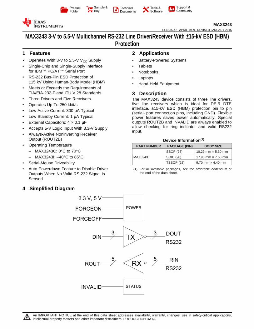
RX TX POWER 3.3 V, 5 V DIN ROUT DOUT RS232 RIN RS232 3 3 5 5 FORCEON FORCEOFF STATUS INVALID Product Folder Sample & Buy Technical Documents Tools & Software Support & Community MAX3243 SLLS350O – APRIL 1999 – REVISED JANUARY 2015 MAX3243 3-V to 5.5-V Multichannel RS-232 Line Driver/Receiver With ±15-kV ESD (HBM) Protection 1 Features 2 Applications 1• Operates With 3-V to 5.5-V V CC Supply • Battery-Powered Systems • Single-Chip and Single-Supply Interface • Tablets for IBM™ PC/AT™ Serial Port • Notebooks • RS-232 Bus-Pin ESD Protection of • Laptops ±15 kV Using Human-Body Model (HBM) • Hand-Held Equipment • Meets or Exceeds the Requirements of TIA/EIA-232-F and ITU V.28 Standards 3 Description • Three Drivers and Five Receivers The MAX3243 device consists of three line drivers, five line receivers which is ideal for DE-9 DTE • Operates Up To 250 kbit/s interface. ±15-kV ESD (HBM) protection pin to pin • Low Active Current: 300 μA Typical (serial- port connection pins, including GND). Flexible • Low Standby Current: 1 μA Typical power features saves power automatically. Special outputs ROUT2B and INVALID are always enabled to • External Capacitors: 4 × 0.1 μF allow checking for ring indicator and valid RS232 • Accepts 5-V Logic Input With 3.3-V Supply input. • Always-Active Noninverting Receiver Output (ROUT2B) Device Information (1) • Operating Temperature PART NUMBER PACKAGE (PIN) BODY SIZE – MAX3243C: 0°C to 70°C SSOP (28) 10.29 mm × 5.30 mm MAX3243 SOIC (28) 17.90 mm × 7.50 mm – MAX3243I: –40°C to 85°C TSSOP (28) 9.70 mm × 4.40 mm • Serial-Mouse Driveability (1) For all available packages, see the orderable addendum at • Auto-Powerdown Feature to Disable Driver the end of the data sheet. Outputs When No Valid RS-232 Signal Is Sensed 4 Simplified Diagram 1 An IMPORTANT NOTICE at the end of this data sheet addresses availability, warranty, changes, use in safety-critical applications, intellectual property matters and other important disclaimers. PRODUCTION DATA.
Transcript of 1 Features 2 Applications 3 Description - Analog, … · RX TX POWER 3.3 V, 5 V DIN ROUT DOUT RS232...
RX
TX
POWER
3.3 V, 5 V
DIN
ROUT
DOUT
RS232
RIN
RS232
3 3
5 5
FORCEON
FORCEOFF
STATUSINVALID
Product
Folder
Sample &Buy
Technical
Documents
Tools &
Software
Support &Community
MAX3243SLLS350O –APRIL 1999–REVISED JANUARY 2015
MAX3243 3-V to 5.5-V Multichannel RS-232 Line Driver/Receiver With ±15-kV ESD (HBM)Protection
1 Features 2 Applications1• Operates With 3-V to 5.5-V VCC Supply • Battery-Powered Systems• Single-Chip and Single-Supply Interface • Tablets
for IBM™ PC/AT™ Serial Port • Notebooks• RS-232 Bus-Pin ESD Protection of • Laptops
±15 kV Using Human-Body Model (HBM) • Hand-Held Equipment• Meets or Exceeds the Requirements of
TIA/EIA-232-F and ITU V.28 Standards 3 Description• Three Drivers and Five Receivers The MAX3243 device consists of three line drivers,
five line receivers which is ideal for DE-9 DTE• Operates Up To 250 kbit/sinterface. ±15-kV ESD (HBM) protection pin to pin• Low Active Current: 300 μA Typical (serial- port connection pins, including GND). Flexible
• Low Standby Current: 1 μA Typical power features saves power automatically. Specialoutputs ROUT2B and INVALID are always enabled to• External Capacitors: 4 × 0.1 μFallow checking for ring indicator and valid RS232• Accepts 5-V Logic Input With 3.3-V Supplyinput.
• Always-Active Noninverting ReceiverOutput (ROUT2B) Device Information(1)
• Operating Temperature PART NUMBER PACKAGE (PIN) BODY SIZE– MAX3243C: 0°C to 70°C SSOP (28) 10.29 mm × 5.30 mm
MAX3243 SOIC (28) 17.90 mm × 7.50 mm– MAX3243I: –40°C to 85°CTSSOP (28) 9.70 mm × 4.40 mm• Serial-Mouse Driveability
(1) For all available packages, see the orderable addendum at• Auto-Powerdown Feature to Disable Driverthe end of the data sheet.Outputs When No Valid RS-232 Signal Is
Sensed
4 Simplified Diagram
1
An IMPORTANT NOTICE at the end of this data sheet addresses availability, warranty, changes, use in safety-critical applications,intellectual property matters and other important disclaimers. PRODUCTION DATA.
MAX3243SLLS350O –APRIL 1999–REVISED JANUARY 2015 www.ti.com
Table of Contents1 Features .................................................................. 1 8 Parameter Measurement Information .................. 82 Applications ........................................................... 1 9 Detailed Description ............................................ 11
9.1 Overview ................................................................. 113 Description ............................................................. 19.2 Functional Block Diagram ....................................... 114 Simplified Diagram ................................................ 19.3 Feature Description................................................. 125 Revision History..................................................... 29.4 Device Functional Modes........................................ 136 Pin Configuration and Functions ......................... 3
10 Application and Implementation........................ 147 Specifications......................................................... 410.1 Application Information.......................................... 147.1 Absolute Maximum Ratings ..................................... 410.2 Typical Application ................................................ 147.2 ESD Ratings.............................................................. 4
11 Power Supply Recommendations ..................... 167.3 Recommended Operating Conditions....................... 412 Layout................................................................... 167.4 Thermal Information .................................................. 4
12.1 Layout Guidelines ................................................. 167.5 Electrical Characteristics –– Auto Power Down........ 512.2 Layout Example .................................................... 177.6 Electrical Characteristics –– Driver .......................... 5
13 Device and Documentation Support ................. 187.7 Electrical Characteristics –– Receiver ..................... 613.1 Trademarks ........................................................... 187.8 Switching Characteristics –– Auto Power Down ...... 613.2 Electrostatic Discharge Caution............................ 187.9 Switching Characteristics –– Driver ......................... 613.3 Glossary ................................................................ 187.10 Switching Characteristics –– Receiver ................... 6
7.11 Typical Characteristics ............................................ 7 14 Mechanical, Packaging, and OrderableInformation ........................................................... 18
5 Revision History
Changes from Revision N (May 2009) to Revision O Page
• Added Applications, Device Information table, Pin Functions table, ESD Ratings table, Thermal Information table,Typical Characteristics, Feature Description section, Device Functional Modes, Application and Implementationsection, Power Supply Recommendations section, Layout section, Device and Documentation Support section, andMechanical, Packaging, and Orderable Information section. ................................................................................................. 1
• Deleted Ordering Information table. ....................................................................................................................................... 1
2 Submit Documentation Feedback Copyright © 1999–2015, Texas Instruments Incorporated
Product Folder Links: MAX3243
1
2
3
4
5
6
7
8
9
10
11
12
13
14
28
27
26
25
24
23
22
21
20
19
18
17
16
15
C2+
C2−
V−
RIN1
RIN2
RIN3
RIN4
RIN5
DOUT1
DOUT2
DOUT3
DIN3
DIN2
DIN1
C1+
V+
VCC
GND
C1−
FORCEON
FORCEOFF
INVALID
ROUT2B
ROUT1
ROUT2
ROUT3
ROUT4
ROUT5
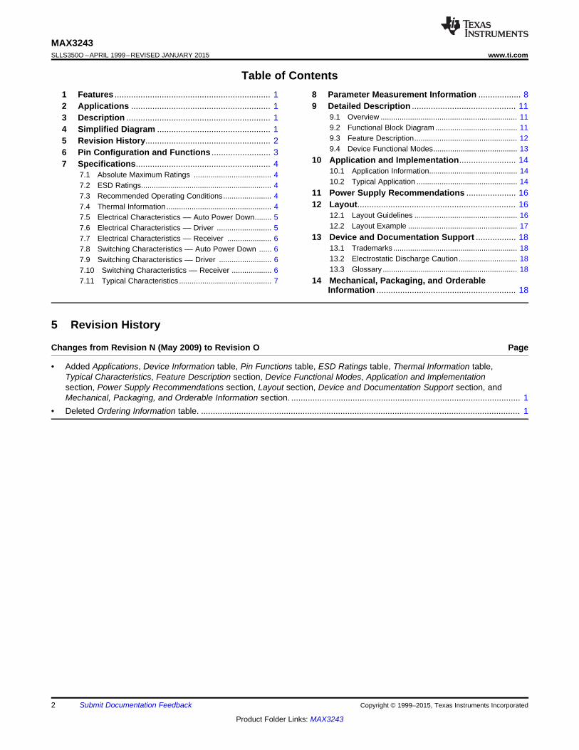
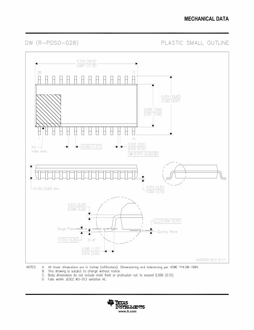
DB, DW, OR PW PACKAGE
(TOP VIEW)
MAX3243www.ti.com SLLS350O –APRIL 1999–REVISED JANUARY 2015
6 Pin Configuration and Functions
Pin FunctionsPIN
TYPE DESCRIPTIONNAME NO.
C2+ 1 — Positive lead of C2 capacitorC2– 2 — Negative lead of C2 capacitorV– 3 O Negative charge pump output for storage capacitor only
RIN1:RIN5 4, 5, 6, 7, 8 I RS232 line data input (from remote RS232 system)DOUT1:DOUT3 9, 10, 11 O RS232 line data output (to remote RS232 system)
DIN3:DIN1 12, 13, 14 I Logic data input (from UART)ROUT5:ROUT1 15, 16, 17, 18, 19 O Logic data output (to UART)
Always Active non-inverting output for RIN2 (normally used for ringROUT2B 20 O indicator)INVALID 21 O Active low output when all RIN are unpowered
Low input forces DOUT1-5, ROUT1-5 high Z per Device FunctionalFORCEOFF 22 I ModesHigh forces drivers on. Low is automatic mode per Device FunctionalFORCEON 23 I Modes
C1– 24 — Negative lead on C1 capacitorGND 25 — GroundVCC 26 — Supply Voltage, Connect to 3V to 5.5V power supplyV+ 27 O Positive charge pump output for storage capacitor only
C1+ 28 — Positive lead of C1 capacitor
Copyright © 1999–2015, Texas Instruments Incorporated Submit Documentation Feedback 3
Product Folder Links: MAX3243
MAX3243SLLS350O –APRIL 1999–REVISED JANUARY 2015 www.ti.com
7 Specifications
7.1 Absolute Maximum Ratingsover operating free-air temperature range (unless otherwise noted) (1)
MIN MAX UNITVCC Supply voltage range (2) –0.3 6 VV+ Positive output supply voltage range (2) –0.3 7 VV– Negative output supply voltage range (2) 0.3 –7 VV+ – V– Supply voltage difference (2) 13 V
Driver, FORCEOFF, FORCEON –0.3 6VI Input voltage range V
Receiver –25 25Driver –13.2 13.2
VO Output voltage range VReceiver, INVALID –0.3 VCC + 0.3
TJ Operating virtual junction temperature 150 °CTstg Storage temperature range –65 150 °C
(1) Stresses beyond those listed under Absolute Maximum Ratings may cause permanent damage to the device. These are stress ratingsonly, and functional operation of the device at these or any other conditions beyond those indicated under Recommended OperatingConditions is not implied. Exposure to absolute-maximum-rated conditions for extended periods may affect device reliability.
(2) All voltages are with respect to network GND.
7.2 ESD RatingsMAX UNIT
Human body model (HBM), per ANSI/ESDA/JEDEC JS-001 15000RIN , DOUT, and GND pins (1)
Human body model (HBM), per ANSI/ESDA/JEDEC JS-001V(ESD) Electrostatic discharge 3000 VAll other pins (1)
Charged device model (CDM), per JEDEC specification JESD22-C101, 1000all pins (2)
(1) JEDEC document JEP155 states that 500-V HBM allows safe manufacturing with a standard ESD control process.(2) JEDEC document JEP157 states that 250-V CDM allows safe manufacturing with a standard ESD control process.
7.3 Recommended Operating Conditions(1)(See Figure 8)
MIN NOM MAX UNITVCC = 3.3 V 3 3.3 3.6
VCC Supply voltage VVCC = 5 V 4.5 5 5.5VCC = 3.3 V 2 5.5DIN, FORCEOFF,VIH Driver and control high-level input voltage VFORCEON VCC = 5 V 2.4 5.5
VIL Driver and control low-level input voltage DIN, FORCEOFF, FORCEON 0 0.8 VVI Driver and control input voltage DIN, FORCEOFF, FORCEON 0 5.5 VVI Receiver input voltage –25 25 V
MAX3243C 0 70TA Operating free-air temperature °C
MAX3243I –40 85
(1) Test conditions are C1–C4 = 0.1 μF at VCC = 3.3 V ± 0.3 V; C1 = 0.047 μF, C2–C4 = 0.33 μF at VCC = 5 V ± 0.5 V.
7.4 Thermal InformationMAX3243
THERMAL METRIC (1) DB DW PW UNIT16 PINS 16 PINS 16 PINS
RθJA Junction-to-ambient thermal resistance 62 46 62 °C/W
(1) For more information about traditional and new thermal metrics, see the IC Package Thermal Metrics application report (SPRA953).
4 Submit Documentation Feedback Copyright © 1999–2015, Texas Instruments Incorporated
Product Folder Links: MAX3243
MAX3243www.ti.com SLLS350O –APRIL 1999–REVISED JANUARY 2015
7.5 Electrical Characteristics –– Auto Power Downover recommended ranges of supply voltage and operating free-air temperature (unless otherwise noted) (1) (see Figure 8)
PARAMETER TEST CONDITIONS MIN TYP (2) MAX UNITSupply currentAuto-powerdown No load, FORCEOFF and FORCEON at VCC. TA = 25°C 0.3 1 mAdisabledSupply currentICC No load, FORCEOFF at GND. TA = 25°C 1 10Powered off
μASupply current No load, FORCEOFF at VCC, FORCEON at GND,Auto-powerdown All RIN are open or grounded, All DIN are grounded. TA = 1 10enabled 25°C
II Input leakage current VI = VCC or VI at GND ±0.01 ±1 μAof FORCEOFF, FORCEONReceiver input threshold FORCEON = GND,VIT+ for INVALID high-level output 2.7 VFORCEOFF = VCCvoltageReceiver input threshold FORCEON = GND,VIT– for INVALID high-level output –2.7 VFORCEOFF = VCCvoltageReceiver input threshold FORCEON = GND,VT for INVALID low-level output –0.3 0.3 VFORCEOFF = VCCvoltageINVALID high-level output IOH = -1 mA, FORCEON = GND,VOH VCC – 0.6 Vvoltage FORCEOFF = VCC
INVALID low-level output IOL = 1.6 mA, FORCEON = GND,VOL 0.4 Vvoltage FORCEOFF = VCC
(1) Test conditions are C1–C4 = 0.1 μF at VCC = 3.3 V ± 0.3 V; C1 = 0.047 μF, C2–C4 = 0.33 μF at VCC = 5 V ± 0.5 V.(2) Stresses beyond those listed under Absolute Maximum Ratings may cause permanent damage to the device. These are stress ratings
only, and functional operation of the device at these or any other conditions beyond those indicated under Recommended OperatingConditions is not implied. Exposure to absolute-maximum-rated conditions for extended periods may affect device reliability.
7.6 Electrical Characteristics –– Driverover recommended ranges of supply voltage and operating free-air temperature (unless otherwise noted) (1) (see Figure 8)
PARAMETER TEST CONDITIONS MIN TYP (2) MAX UNITVOH High-level output voltage All DOUT at RL = 3 kΩ to GND 5 5.4 VVOL Low-level output voltage All DOUT at RL = 3 kΩ to GND –5 –5.4 V
Output voltage DIN1 = DIN2 = GND, DIN3 = VCC, 3-kΩ to GND at DOUT3,VO ±5 V(mouse driveability) DOUT1 = DOUT2 = 2.5 mAIIH High-level input current VI = VCC ±0.01 ±1 μAIIL Low-level input current VI at GND ±0.01 ±1 μAVhys Input hysteresis ±1 V
VCC = 3.6 V, VO = 0 VIOS Short-circuit output current (3) ±35 ±60 mA
VCC = 5.5 V, VO = 0 Vro Output resistance VCC, V+, and V– = 0 V, VO = ±2 V 300 10M Ω
VO = ±12 V, VCC = 3 to 3.6 V ±25Ioff Output leakage current FORCEOFF = GND, μA
VO = ±10 V, VCC = 4.5 to 5.5 V ±25
(1) Test conditions are C1–C4 = 0.1 μF at VCC = 3.3 V ± 0.3 V; C1 = 0.047 μF, C2–C4 = 0.33 μF at VCC = 5 V ± 0.5 V.(2) All typical values are at VCC = 3.3 V or VCC = 5 V, and TA = 25°C.(3) Short-circuit durations should be controlled to prevent exceeding the device absolute power dissipation ratings, and not more than one
output should be shorted at a time.
Copyright © 1999–2015, Texas Instruments Incorporated Submit Documentation Feedback 5
Product Folder Links: MAX3243
MAX3243SLLS350O –APRIL 1999–REVISED JANUARY 2015 www.ti.com
7.7 Electrical Characteristics –– Receiverover recommended ranges of supply voltage and operating free-air temperature (unless otherwise noted) (1) (see Figure 8)
PARAMETER TEST CONDITIONS MIN TYP (2) MAX UNITVOH High-level output voltage IOH = –1 mA VCC – 0.6 VCC – 0.1 VVOL Low-level output voltage IOH = 1.6 mA 0.4 V
VCC = 3.3 V 1.6 2.4VIT+ Positive-going input threshold voltage V
VCC = 5 V 1.9 2.4VCC = 3.3 V 0.6 1.1
VIT– Negative-going input threshold voltage VVCC = 5 V 0.8 1.4
Vhys Input hysteresis (VIT+ – VIT–) 0.5 VIoff Output leakage current (except ROUT2B) FORCEOFF = 0 V ±0.05 ±10 μArI Input resistance VI = ±3 V or ±25 V 3 5 7 kΩ
(1) Test conditions are C1–C4 = 0.1 μF at VCC = 3.3 V ± 0.3 V; C1 = 0.047 μF, C2–C4 = 0.33 μF at VCC = 5 V ± 0.5 V.(2) All typical values are at VCC = 3.3 V or VCC = 5 V, and TA = 25°C.
7.8 Switching Characteristics –– Auto Power Downover recommended ranges of supply voltage and operating free-air temperature (unless otherwise noted) (see Figure 7)
PARAMETER TEST CONDITIONS TYP (1) UNITtvalid Propagation delay time, low- to high-level output VCC = 5 V 1 μstinvalid Propagation delay time, high- to low-level output VCC = 5 V 30 μsten Supply enable time VCC = 5 V 100 μs
(1) All typical values are at VCC = 3.3 V or VCC = 5 V, and TA = 25°C.
7.9 Switching Characteristics –– Driverover recommended ranges of supply voltage and operating free-air temperature (unless otherwise noted) (1) (see Figure 8)MAX3243C, MAX3243I
PARAMETER TEST CONDITIONS MIN TYP (2) MAX UNITRL = 3 kΩ CL = 1000 pFMaximum data rate 150 250 kbit/sOne DOUT switching, See Figure 3
CL = 150 pF to 2500 pFtsk(p) Pulse skew (3) RL = 3 kΩ to 7 kΩ 100 nsSee Figure 5CL = 150 pF to 1000 pF 6 30Slew rate, transition region VCC = 3.3 V,SR(tr) V/μs(see Figure 3) RL = 3 kΩ to 7 kΩ CL = 150 pF to 2500 pF 4 30
(1) Test conditions are C1–C4 = 0.1 μF at VCC = 3.3 V + 0.3 V; C1 = 0.047 μF, C2–C4 = 0.33 μF at VCC = 5 V ± 0.5 V.(2) All typical values are at VCC = 3.3 V or VCC = 5 V, and TA = 25°C.(3) Pulse skew is defined as |tPLH – tPHL| of each channel of the same device.
7.10 Switching Characteristics –– Receiverover recommended ranges of supply voltage and operating free-air temperature (unless otherwise noted) (1)
PARAMETER TEST CONDITIONS TYP (2) UNITtPLH Propagation delay time, low- to high-level output 150 nsCL = 150 pF,
See Figure 5tPHL Propagation delay time, high- to low-level output 150 nsten Output enable time 200 nsCL = 150 pF, RL = 3 kΩ,
See Figure 6tdis Output disable time 200 nstsk(p) Pulse skew (3) See Figure 5 50 ns
(1) Test conditions are C1–C4 = 0.1 μF at VCC = 3.3 V ± 0.3 V; C1 = 0.047 μF, C2–C4 = 0.33 μF at VCC = 5 V ± 0.5 V.(2) All typical values are at VCC = 3.3 V or VCC = 5 V, and TA = 25°C.(3) Pulse skew is defined as |tPLH - tPHL| of each channel of the same device.
6 Submit Documentation Feedback Copyright © 1999–2015, Texas Instruments Incorporated
Product Folder Links: MAX3243
0
1
2
3
4
5
6
0 5 10 15 20 25 30 35
VO
H (
V)
Load Current (mA)
VOH
C001
±6
±5
±4
±3
±2
±1
0
0 5 10 15 20 25 30 35
VO
L (V
)
Load Current (mA)
VOL
C001
MAX3243www.ti.com SLLS350O –APRIL 1999–REVISED JANUARY 2015
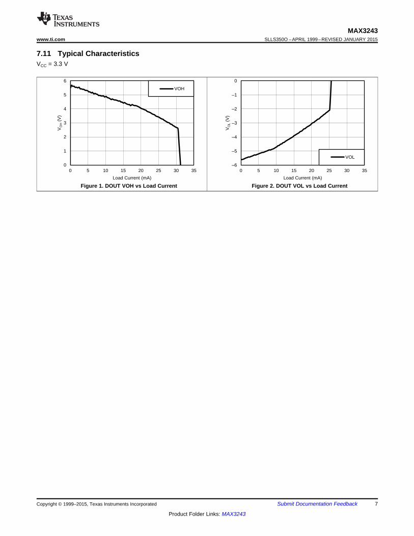
7.11 Typical CharacteristicsVCC = 3.3 V
Figure 1. DOUT VOH vs Load Current Figure 2. DOUT VOL vs Load Current
Copyright © 1999–2015, Texas Instruments Incorporated Submit Documentation Feedback 7
Product Folder Links: MAX3243
TEST CIRCUIT VOLTAGE WAVEFORMS
50 W
−3 V
3 V
Output
Input
VOL
VOH
tPHLGenerator
(see Note B)tPLH
Output
CL
(see Note A)
3 V or 0 V
FORCEON
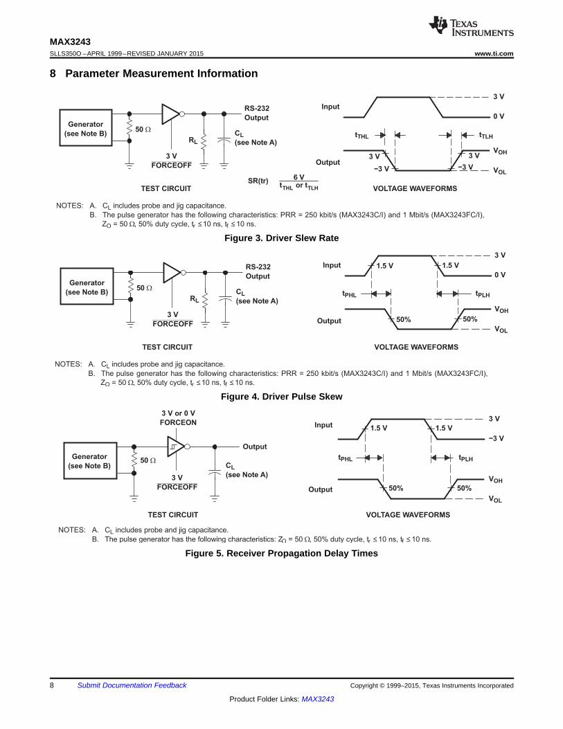
NOTES: A. CL includes probe and jig capacitance.
B. The pulse generator has the following characteristics: ZO = 50 W, 50% duty cycle, tr ≤10 ns, tf ≤10 ns.
3 V
FORCEOFF
1.5 V 1.5 V
50% 50%
50 W
TEST CIRCUIT VOLTAGE WAVEFORMS
0 V
3 V
Output
Input
VOL
VOH
tPLH
Generator
(see Note B)RL
3 V
FORCEOFF
RS-232
Output
tPHLCL
(see Note A)
NOTES: A. CL includes probe and jig capacitance.
B. The pulse generator has the following characteristics: PRR = 250 kbit/s (MAX3243C/I) and 1 Mbit/s (MAX3243FC/I),
ZO = 50 W, 50% duty cycle, tr ≤10 ns, tf ≤10 ns.
50% 50%
1.5 V 1.5 V
50 W
TEST CIRCUIT VOLTAGE WAVEFORMS
−3 V−3 V
3 V3 V
0 V
3 V
Output
Input
VOL
VOH
tTLH
Generator
(see Note B)RL
3 V
FORCEOFF
RS-232
Output
tTHLCL
(see Note A)
SR(tr)6 V
tTHL or tTLH
NOTES: A. CL includes probe and jig capacitance.
B. The pulse generator has the following characteristics: PRR = 250 kbit/s (MAX3243C/I) and 1 Mbit/s (MAX3243FC/I),
ZO = 50 W, 50% duty cycle, tr ≤10 ns, tf ≤10 ns.
MAX3243SLLS350O –APRIL 1999–REVISED JANUARY 2015 www.ti.com
8 Parameter Measurement Information
Figure 3. Driver Slew Rate
Figure 4. Driver Pulse Skew
Figure 5. Receiver Propagation Delay Times
8 Submit Documentation Feedback Copyright © 1999–2015, Texas Instruments Incorporated
Product Folder Links: MAX3243
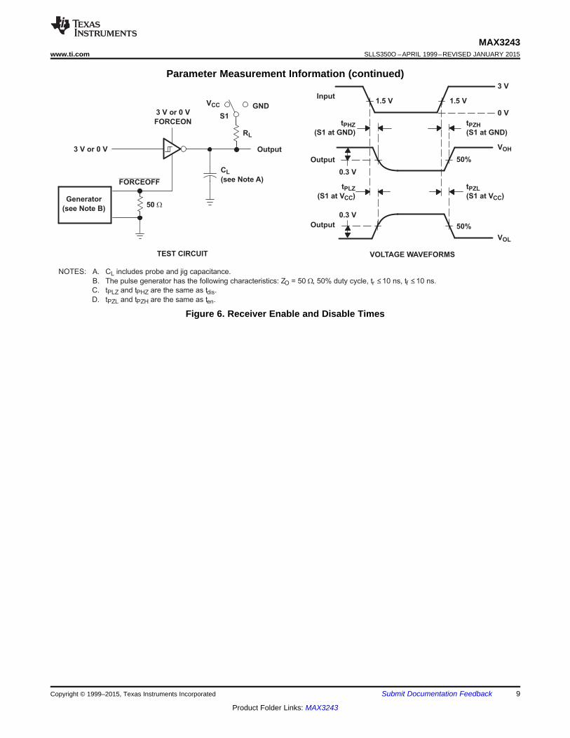
TEST CIRCUIT
50 WGenerator
(see Note B)
3 V or 0 V
3 V or 0 V
FORCEON
FORCEOFF
NOTES: A. CL includes probe and jig capacitance.
B. The pulse generator has the following characteristics: ZO = 50 W, 50% duty cycle, tr ≤10 ns, tf ≤10 ns.
C. tPLZ and tPHZ are the same as tdis.
D. tPZL and tPZH are the same as ten.
RL
S1
VCC GND
CL
(see Note A)
Output
VOLTAGE WAVEFORMS
Output
VOL
VOH
tPZH
(S1 at GND)
3 V
0 V
0.3 V
Output
Input
0.3 V
1.5 V 1.5 V
50%
tPHZ
(S1 at GND)
tPLZ
(S1 at VCC)
50%
tPZL
(S1 at VCC)
MAX3243www.ti.com SLLS350O –APRIL 1999–REVISED JANUARY 2015
Parameter Measurement Information (continued)
Figure 6. Receiver Enable and Disable Times
Copyright © 1999–2015, Texas Instruments Incorporated Submit Documentation Feedback 9
Product Folder Links: MAX3243
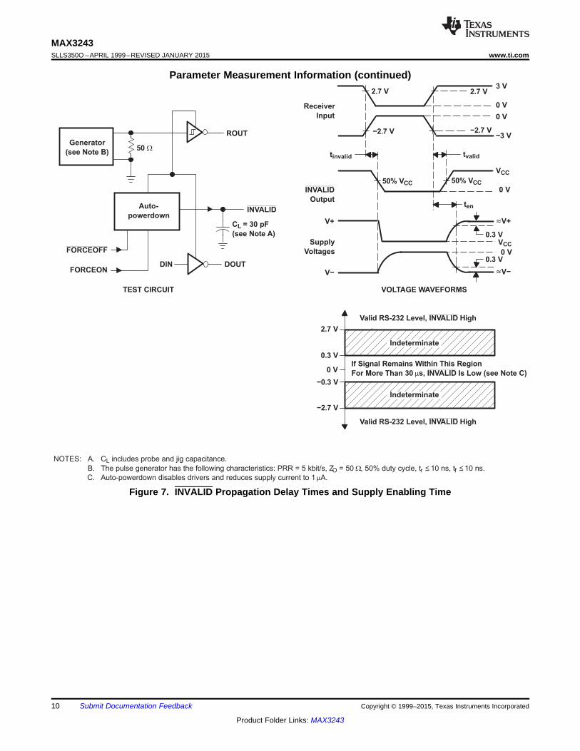
TEST CIRCUIT VOLTAGE WAVEFORMS
50 W
3 V2.7 V
−2.7 V
INVALID
Output
Receiver
Input
Generator
(see Note B)
FORCEOFF
tvalid
ROUT
FORCEON
Auto-
powerdownINVALID
DOUT
0 V
0 V
−3 V
DIN
CL = 30 pF
(see Note A)
VCC
0 V
2.7 V
−2.7 V
0.3 V
−0.3 V
0 V
Valid RS-232 Level, INVALID High
Indeterminate
Indeterminate
If Signal Remains Within This Region
For More Than 30 ms, INVALID Is Low (see Note C)
Valid RS-232 Level, INVALID High
≈V+
0 V
≈V−
V+
VCC
ten
V−
NOTES: A. CL includes probe and jig capacitance.
B. The pulse generator has the following characteristics: PRR = 5 kbit/s, ZO = 50 W, 50% duty cycle, tr ≤10 ns, tf ≤10 ns.
C. Auto-powerdown disables drivers and reduces supply current to 1mA.
50% VCC 50% VCC
2.7 V
−2.7 V
0.3 V
0.3 V
tinvalid
Supply
Voltages
MAX3243SLLS350O –APRIL 1999–REVISED JANUARY 2015 www.ti.com
Parameter Measurement Information (continued)
Figure 7. INVALID Propagation Delay Times and Supply Enabling Time
10 Submit Documentation Feedback Copyright © 1999–2015, Texas Instruments Incorporated
Product Folder Links: MAX3243
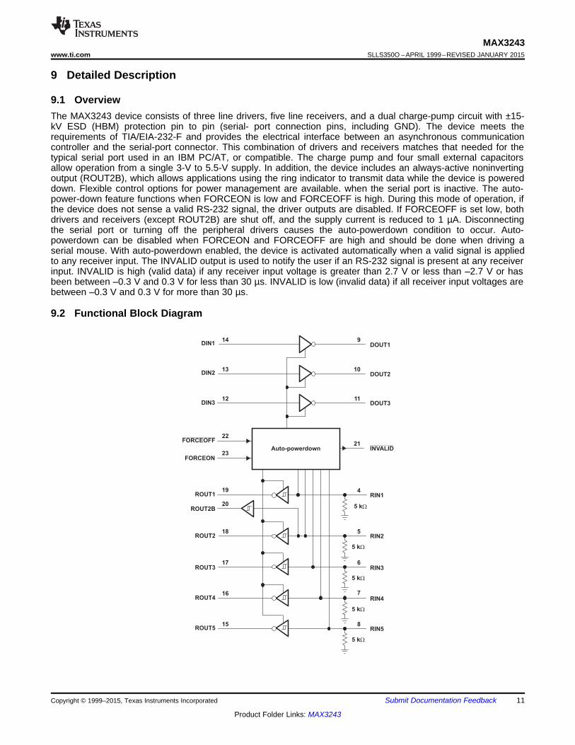
DIN3
DIN2
DIN1
DOUT3
DOUT2
DOUT1
Auto-powerdown INVALID
RIN1
RIN2
RIN3
RIN4
RIN5
FORCEOFF
FORCEON
ROUT1
ROUT2B
ROUT2
ROUT3
ROUT4
ROUT5
14
13
12
22
23
19
20
18
17
16
15
9
10
11
21
4
5
6
7
8
5 k
5 k
5 k
5 k
5 k
W
W
W
W
W
MAX3243www.ti.com SLLS350O –APRIL 1999–REVISED JANUARY 2015
9 Detailed Description
9.1 OverviewThe MAX3243 device consists of three line drivers, five line receivers, and a dual charge-pump circuit with ±15-kV ESD (HBM) protection pin to pin (serial- port connection pins, including GND). The device meets therequirements of TIA/EIA-232-F and provides the electrical interface between an asynchronous communicationcontroller and the serial-port connector. This combination of drivers and receivers matches that needed for thetypical serial port used in an IBM PC/AT, or compatible. The charge pump and four small external capacitorsallow operation from a single 3-V to 5.5-V supply. In addition, the device includes an always-active noninvertingoutput (ROUT2B), which allows applications using the ring indicator to transmit data while the device is powereddown. Flexible control options for power management are available. when the serial port is inactive. The auto-power-down feature functions when FORCEON is low and FORCEOFF is high. During this mode of operation, ifthe device does not sense a valid RS-232 signal, the driver outputs are disabled. If FORCEOFF is set low, bothdrivers and receivers (except ROUT2B) are shut off, and the supply current is reduced to 1 µA. Disconnectingthe serial port or turning off the peripheral drivers causes the auto-powerdown condition to occur. Auto-powerdown can be disabled when FORCEON and FORCEOFF are high and should be done when driving aserial mouse. With auto-powerdown enabled, the device is activated automatically when a valid signal is appliedto any receiver input. The INVALID output is used to notify the user if an RS-232 signal is present at any receiverinput. INVALID is high (valid data) if any receiver input voltage is greater than 2.7 V or less than –2.7 V or hasbeen between –0.3 V and 0.3 V for less than 30 µs. INVALID is low (invalid data) if all receiver input voltages arebetween –0.3 V and 0.3 V for more than 30 µs.
9.2 Functional Block Diagram
Copyright © 1999–2015, Texas Instruments Incorporated Submit Documentation Feedback 11
Product Folder Links: MAX3243
MAX3243SLLS350O –APRIL 1999–REVISED JANUARY 2015 www.ti.com
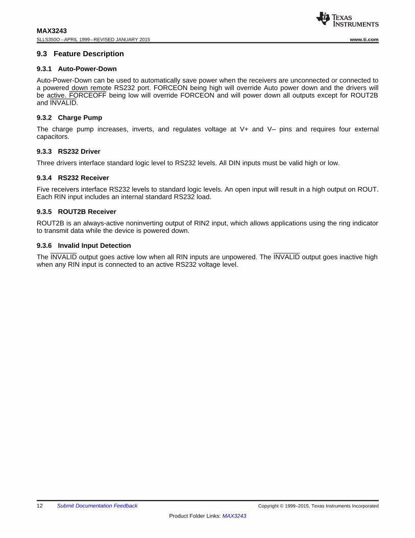
9.3 Feature Description
9.3.1 Auto-Power-DownAuto-Power-Down can be used to automatically save power when the receivers are unconnected or connected toa powered down remote RS232 port. FORCEON being high will override Auto power down and the drivers willbe active. FORCEOFF being low will override FORCEON and will power down all outputs except for ROUT2Band INVALID.
9.3.2 Charge PumpThe charge pump increases, inverts, and regulates voltage at V+ and V– pins and requires four externalcapacitors.
9.3.3 RS232 DriverThree drivers interface standard logic level to RS232 levels. All DIN inputs must be valid high or low.
9.3.4 RS232 ReceiverFive receivers interface RS232 levels to standard logic levels. An open input will result in a high output on ROUT.Each RIN input includes an internal standard RS232 load.
9.3.5 ROUT2B ReceiverROUT2B is an always-active noninverting output of RIN2 input, which allows applications using the ring indicatorto transmit data while the device is powered down.
9.3.6 Invalid Input DetectionThe INVALID output goes active low when all RIN inputs are unpowered. The INVALID output goes inactive highwhen any RIN input is connected to an active RS232 voltage level.
12 Submit Documentation Feedback Copyright © 1999–2015, Texas Instruments Incorporated
Product Folder Links: MAX3243
MAX3243www.ti.com SLLS350O –APRIL 1999–REVISED JANUARY 2015
9.4 Device Functional Modes
Table 1. Each Driver (1)
INPUTS OUTPUTDRIVER STATUSVALID RINDIN FORCEON FORCEOFF DOUTRS-232 LEVEL
X X L X Z Powered offL H H X H Normal operation with
auto-powerdown disabledH H H X LL L H YES H Normal operation with
auto-powerdown enabledH L H YES LPower off byX L H NO Z auto-powerdown feature
(1) H = high level, L = low level, X = irrelevant, Z = high impedance, YES = any RIN valid, NO = all RIN invalid
Table 2. Each Receiver (1)
INPUTS OUTPUTSRECEIVER STATUS
RIN FORCEON FORCEOFF ROUTX X L Z Powered offL X H HH X H L Normal operation
Open X H H
(1) H = high level, L = low level, X = irrelevant, Z = high impedance (off), Open = input disconnected or connected driver off
Table 3. INVALID and ROUT2B Outputs (1)
INPUTS OUTPUTSVALID RIN OUTPUT STATUS
RS-232 RIN2 FORCEON FORCEOFF INVALID ROUT2BLEVEL
YES L X X H LAlways Active
YES H X X H HYES OPEN X X H L
Always ActiveNO OPEN X X L L
(1) H = high level, L = low level, X = irrelevant, Z = high impedance (off),OPEN = input disconnected or connected driver off, YES = any RIN valid, NO = all RIN invalid
Copyright © 1999–2015, Texas Instruments Incorporated Submit Documentation Feedback 13
Product Folder Links: MAX3243
RIN4
DOUT2
DOUT3
ROUT1
FORCEOFF
RIN5
INVALID
ROUT2
DOUT1 ROUT2B
DIN3
DIN2
ROUT3
ROUT4
DIN1 ROUT5
C4+
−
+
−
C3(1)
VCC
C2+
C2− C1
C1+
GNDV−
C1−
FORCEON
C2+
−
CBYPASS
= 0.1 mF
V+
+
−
+
−
RIN1
RIN2
RIN3RS-232 Inputs
Logic Outputs
Logic Inputs
RS-232 Outputs
VCC C1 C2, C3, and C4
3.3 V ± 0.3 V
5 V ± 0.5 V
3 V to 5.5 V
0.1 mF
0.047 mF
0.1 mF
0.1 mF
0.33 mF
0.47 mF
(1) C3 can be connected to VCC or GND.
NOTES: A. Resistor values shown are nominal.
B. Nonpolarized ceramic capacitors are acceptable. If polarized tantalum
or electrolytic capacitors are used, they should be connected as
shown.
VCC vs CAPACITOR VALUES
Au
to-
po
we
rdo
wn
1
2
4
5
6
7
8
9
10
11
12
13
14
3
28
27
26
25
24
23
22
21
20
19
18
17
16
15
5 kW
5 kW
5 kW
5 kW
5 kW
MAX3243SLLS350O –APRIL 1999–REVISED JANUARY 2015 www.ti.com
10 Application and Implementation
NOTEInformation in the following applications sections is not part of the TI componentspecification, and TI does not warrant its accuracy or completeness. TI’s customers areresponsible for determining suitability of components for their purposes. Customers shouldvalidate and test their design implementation to confirm system functionality.
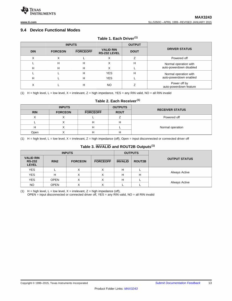
10.1 Application InformationIt is recommended to add capacitors as shown in Figure 8.
10.2 Typical ApplicationROUT and DIN connect to UART or general purpose logic lines. RIN and DOUT lines connect to a RS232connector or cable.
Figure 8. Typical Operating Circuit and Capacitor Values14 Submit Documentation Feedback Copyright © 1999–2015, Texas Instruments Incorporated
Product Folder Links: MAX3243
±9 ±8 ±7 ±6 ±5 ±4 ±3 ±2 ±1
0123456
0 1 2 3 4 5 6 7
Vol
tage
(V
)
Time (s)
DINDOUT to RINROUT
C001
MAX3243www.ti.com SLLS350O –APRIL 1999–REVISED JANUARY 2015
Typical Application (continued)10.2.1 Design Requirements• VCC minimum is 3 V and maximum is 5.5V.• Maximum recommended bit rate is 250 kbit/s.
10.2.2 Detailed Design Procedure• All DIN, FORCEOFF and FORCEON inputs must be connected to valid low or high logic levels.• Select capacitor values based on VCC level for best performance.
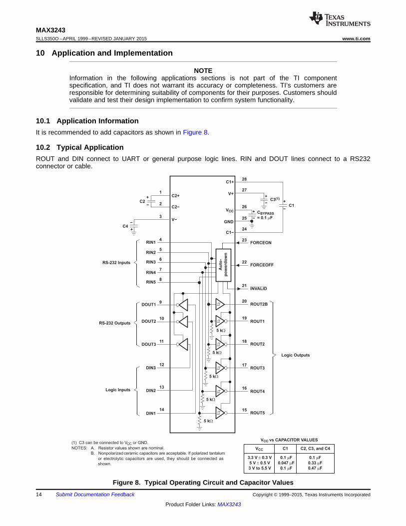
10.2.3 Application CurvesVCC= 3.3 V
Figure 9. Driver to Receiver Loopback Timing Waveform
Copyright © 1999–2015, Texas Instruments Incorporated Submit Documentation Feedback 15
Product Folder Links: MAX3243
MAX3243SLLS350O –APRIL 1999–REVISED JANUARY 2015 www.ti.com
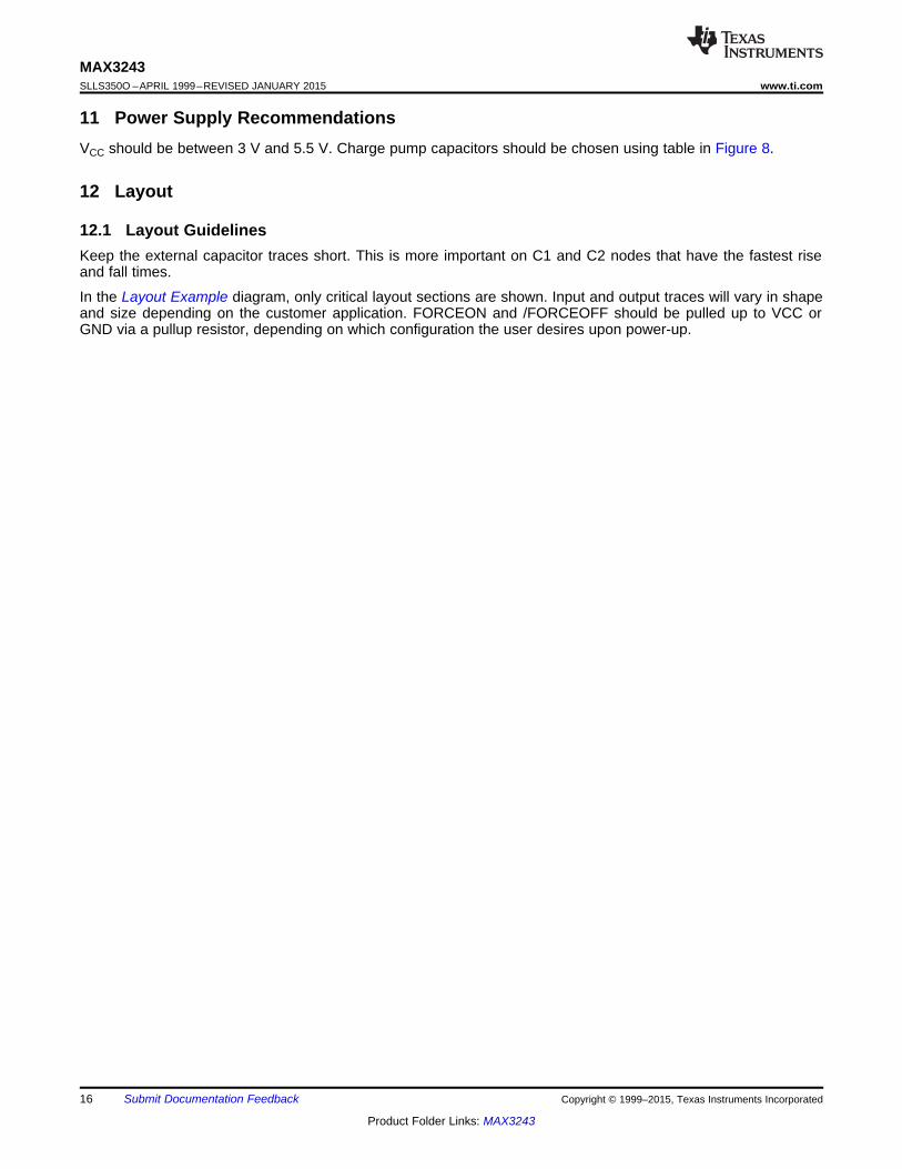
11 Power Supply RecommendationsVCC should be between 3 V and 5.5 V. Charge pump capacitors should be chosen using table in Figure 8.
12 Layout
12.1 Layout GuidelinesKeep the external capacitor traces short. This is more important on C1 and C2 nodes that have the fastest riseand fall times.
In the Layout Example diagram, only critical layout sections are shown. Input and output traces will vary in shapeand size depending on the customer application. FORCEON and /FORCEOFF should be pulled up to VCC orGND via a pullup resistor, depending on which configuration the user desires upon power-up.
16 Submit Documentation Feedback Copyright © 1999–2015, Texas Instruments Incorporated
Product Folder Links: MAX3243
VCC
Ground
Ground 26
25
27
24
23
22
21
28
C2
C40.1 Fμ
C2+
C2-
V-
RIN1
RIN2
RIN3
RIN4
RIN5
C1+
V+
VCC
GND
C1-
FORCEON
FORCEOFF
INVALID
DOUT1
DOUT2
DOUT3
DIN3
DIN2
DIN1
3
4
2
5
6
7
1
10
11
9
12
13
14
8
19
18
20
17
16
15
ROUT2B
ROUT1
ROUT2
ROUT3
ROUT4
ROUT5
C3
Ground
C1
MAX3243www.ti.com SLLS350O –APRIL 1999–REVISED JANUARY 2015
12.2 Layout Example
Figure 10. Layout Diagram
Copyright © 1999–2015, Texas Instruments Incorporated Submit Documentation Feedback 17
Product Folder Links: MAX3243
MAX3243SLLS350O –APRIL 1999–REVISED JANUARY 2015 www.ti.com
13 Device and Documentation Support
13.1 TrademarksIBM, PC/AT are trademarks of IBM.All other trademarks are the property of their respective owners.
13.2 Electrostatic Discharge CautionThese devices have limited built-in ESD protection. The leads should be shorted together or the device placed in conductive foamduring storage or handling to prevent electrostatic damage to the MOS gates.
13.3 GlossarySLYZ022 — TI Glossary.
This glossary lists and explains terms, acronyms, and definitions.
14 Mechanical, Packaging, and Orderable InformationThe following pages include mechanical, packaging, and orderable information. This information is the mostcurrent data available for the designated devices. This data is subject to change without notice and revision ofthis document. For browser-based versions of this data sheet, refer to the left-hand navigation.
18 Submit Documentation Feedback Copyright © 1999–2015, Texas Instruments Incorporated
Product Folder Links: MAX3243
PACKAGE OPTION ADDENDUM
www.ti.com 15-Apr-2017
Addendum-Page 1
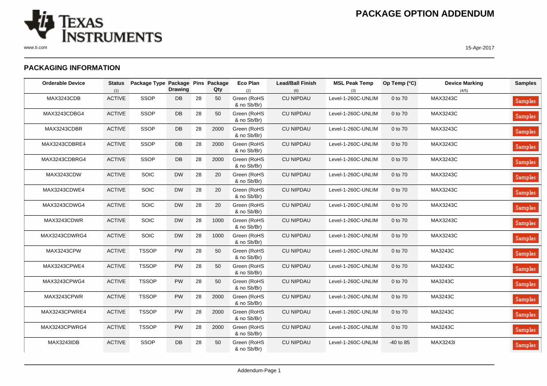
PACKAGING INFORMATION
Orderable Device Status(1)
Package Type PackageDrawing
Pins PackageQty
Eco Plan(2)
Lead/Ball Finish(6)
MSL Peak Temp(3)
Op Temp (°C) Device Marking(4/5)
Samples
MAX3243CDB ACTIVE SSOP DB 28 50 Green (RoHS& no Sb/Br)
CU NIPDAU Level-1-260C-UNLIM 0 to 70 MAX3243C
MAX3243CDBG4 ACTIVE SSOP DB 28 50 Green (RoHS& no Sb/Br)
CU NIPDAU Level-1-260C-UNLIM 0 to 70 MAX3243C
MAX3243CDBR ACTIVE SSOP DB 28 2000 Green (RoHS& no Sb/Br)
CU NIPDAU Level-1-260C-UNLIM 0 to 70 MAX3243C
MAX3243CDBRE4 ACTIVE SSOP DB 28 2000 Green (RoHS& no Sb/Br)
CU NIPDAU Level-1-260C-UNLIM 0 to 70 MAX3243C
MAX3243CDBRG4 ACTIVE SSOP DB 28 2000 Green (RoHS& no Sb/Br)
CU NIPDAU Level-1-260C-UNLIM 0 to 70 MAX3243C
MAX3243CDW ACTIVE SOIC DW 28 20 Green (RoHS& no Sb/Br)
CU NIPDAU Level-1-260C-UNLIM 0 to 70 MAX3243C
MAX3243CDWE4 ACTIVE SOIC DW 28 20 Green (RoHS& no Sb/Br)
CU NIPDAU Level-1-260C-UNLIM 0 to 70 MAX3243C
MAX3243CDWG4 ACTIVE SOIC DW 28 20 Green (RoHS& no Sb/Br)
CU NIPDAU Level-1-260C-UNLIM 0 to 70 MAX3243C
MAX3243CDWR ACTIVE SOIC DW 28 1000 Green (RoHS& no Sb/Br)
CU NIPDAU Level-1-260C-UNLIM 0 to 70 MAX3243C
MAX3243CDWRG4 ACTIVE SOIC DW 28 1000 Green (RoHS& no Sb/Br)
CU NIPDAU Level-1-260C-UNLIM 0 to 70 MAX3243C
MAX3243CPW ACTIVE TSSOP PW 28 50 Green (RoHS& no Sb/Br)
CU NIPDAU Level-1-260C-UNLIM 0 to 70 MA3243C
MAX3243CPWE4 ACTIVE TSSOP PW 28 50 Green (RoHS& no Sb/Br)
CU NIPDAU Level-1-260C-UNLIM 0 to 70 MA3243C
MAX3243CPWG4 ACTIVE TSSOP PW 28 50 Green (RoHS& no Sb/Br)
CU NIPDAU Level-1-260C-UNLIM 0 to 70 MA3243C
MAX3243CPWR ACTIVE TSSOP PW 28 2000 Green (RoHS& no Sb/Br)
CU NIPDAU Level-1-260C-UNLIM 0 to 70 MA3243C
MAX3243CPWRE4 ACTIVE TSSOP PW 28 2000 Green (RoHS& no Sb/Br)
CU NIPDAU Level-1-260C-UNLIM 0 to 70 MA3243C
MAX3243CPWRG4 ACTIVE TSSOP PW 28 2000 Green (RoHS& no Sb/Br)
CU NIPDAU Level-1-260C-UNLIM 0 to 70 MA3243C
MAX3243IDB ACTIVE SSOP DB 28 50 Green (RoHS& no Sb/Br)
CU NIPDAU Level-1-260C-UNLIM -40 to 85 MAX3243I
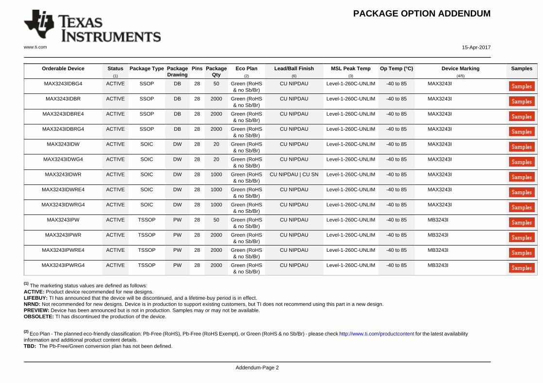
PACKAGE OPTION ADDENDUM
www.ti.com 15-Apr-2017
Addendum-Page 2
Orderable Device Status(1)
Package Type PackageDrawing
Pins PackageQty
Eco Plan(2)
Lead/Ball Finish(6)
MSL Peak Temp(3)
Op Temp (°C) Device Marking(4/5)
Samples
MAX3243IDBG4 ACTIVE SSOP DB 28 50 Green (RoHS& no Sb/Br)
CU NIPDAU Level-1-260C-UNLIM -40 to 85 MAX3243I
MAX3243IDBR ACTIVE SSOP DB 28 2000 Green (RoHS& no Sb/Br)
CU NIPDAU Level-1-260C-UNLIM -40 to 85 MAX3243I
MAX3243IDBRE4 ACTIVE SSOP DB 28 2000 Green (RoHS& no Sb/Br)
CU NIPDAU Level-1-260C-UNLIM -40 to 85 MAX3243I
MAX3243IDBRG4 ACTIVE SSOP DB 28 2000 Green (RoHS& no Sb/Br)
CU NIPDAU Level-1-260C-UNLIM -40 to 85 MAX3243I
MAX3243IDW ACTIVE SOIC DW 28 20 Green (RoHS& no Sb/Br)
CU NIPDAU Level-1-260C-UNLIM -40 to 85 MAX3243I
MAX3243IDWG4 ACTIVE SOIC DW 28 20 Green (RoHS& no Sb/Br)
CU NIPDAU Level-1-260C-UNLIM -40 to 85 MAX3243I
MAX3243IDWR ACTIVE SOIC DW 28 1000 Green (RoHS& no Sb/Br)
CU NIPDAU | CU SN Level-1-260C-UNLIM -40 to 85 MAX3243I
MAX3243IDWRE4 ACTIVE SOIC DW 28 1000 Green (RoHS& no Sb/Br)
CU NIPDAU Level-1-260C-UNLIM -40 to 85 MAX3243I
MAX3243IDWRG4 ACTIVE SOIC DW 28 1000 Green (RoHS& no Sb/Br)
CU NIPDAU Level-1-260C-UNLIM -40 to 85 MAX3243I
MAX3243IPW ACTIVE TSSOP PW 28 50 Green (RoHS& no Sb/Br)
CU NIPDAU Level-1-260C-UNLIM -40 to 85 MB3243I
MAX3243IPWR ACTIVE TSSOP PW 28 2000 Green (RoHS& no Sb/Br)
CU NIPDAU Level-1-260C-UNLIM -40 to 85 MB3243I
MAX3243IPWRE4 ACTIVE TSSOP PW 28 2000 Green (RoHS& no Sb/Br)
CU NIPDAU Level-1-260C-UNLIM -40 to 85 MB3243I
MAX3243IPWRG4 ACTIVE TSSOP PW 28 2000 Green (RoHS& no Sb/Br)
CU NIPDAU Level-1-260C-UNLIM -40 to 85 MB3243I
(1) The marketing status values are defined as follows:ACTIVE: Product device recommended for new designs.LIFEBUY: TI has announced that the device will be discontinued, and a lifetime-buy period is in effect.NRND: Not recommended for new designs. Device is in production to support existing customers, but TI does not recommend using this part in a new design.PREVIEW: Device has been announced but is not in production. Samples may or may not be available.OBSOLETE: TI has discontinued the production of the device.
(2) Eco Plan - The planned eco-friendly classification: Pb-Free (RoHS), Pb-Free (RoHS Exempt), or Green (RoHS & no Sb/Br) - please check http://www.ti.com/productcontent for the latest availabilityinformation and additional product content details.TBD: The Pb-Free/Green conversion plan has not been defined.
PACKAGE OPTION ADDENDUM
www.ti.com 15-Apr-2017
Addendum-Page 3
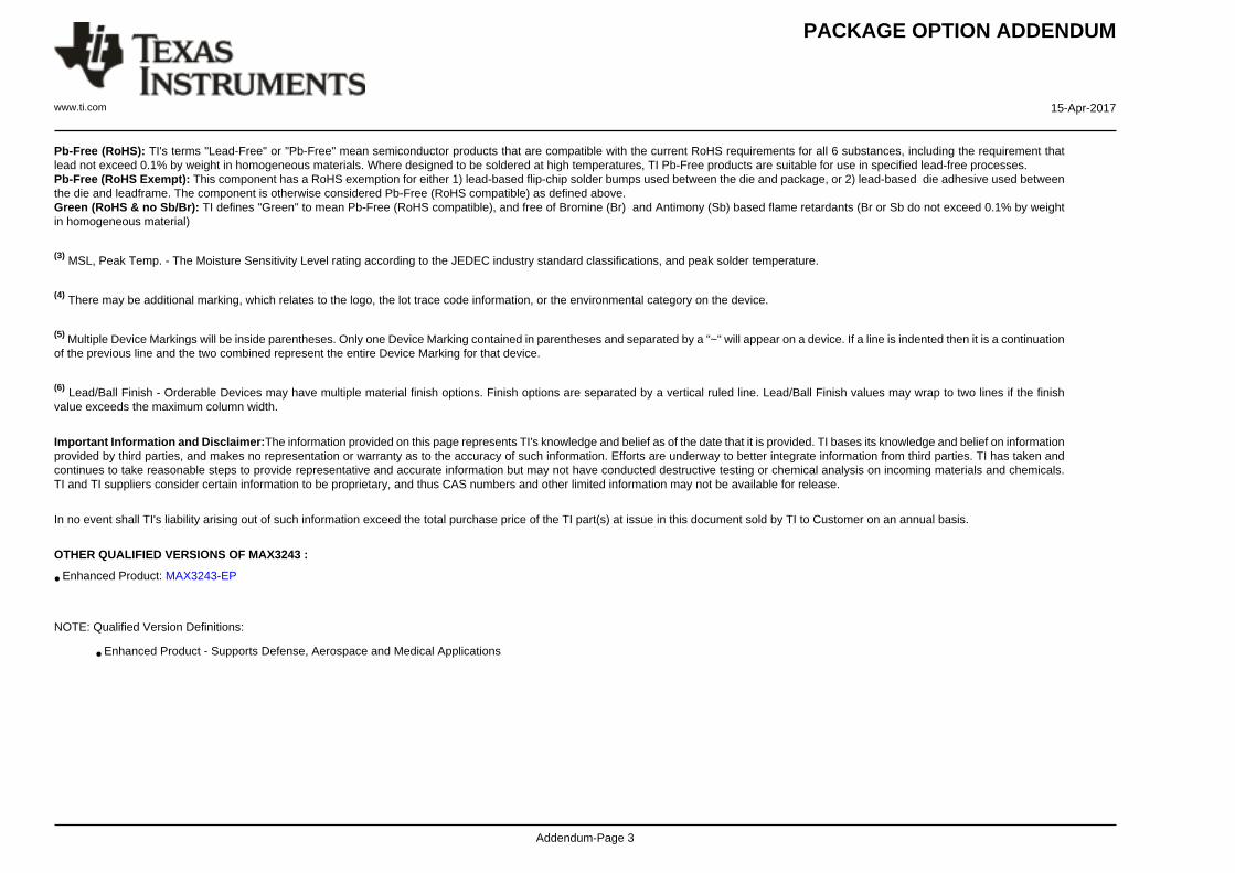
Pb-Free (RoHS): TI's terms "Lead-Free" or "Pb-Free" mean semiconductor products that are compatible with the current RoHS requirements for all 6 substances, including the requirement thatlead not exceed 0.1% by weight in homogeneous materials. Where designed to be soldered at high temperatures, TI Pb-Free products are suitable for use in specified lead-free processes.Pb-Free (RoHS Exempt): This component has a RoHS exemption for either 1) lead-based flip-chip solder bumps used between the die and package, or 2) lead-based die adhesive used betweenthe die and leadframe. The component is otherwise considered Pb-Free (RoHS compatible) as defined above.Green (RoHS & no Sb/Br): TI defines "Green" to mean Pb-Free (RoHS compatible), and free of Bromine (Br) and Antimony (Sb) based flame retardants (Br or Sb do not exceed 0.1% by weightin homogeneous material)
(3) MSL, Peak Temp. - The Moisture Sensitivity Level rating according to the JEDEC industry standard classifications, and peak solder temperature.
(4) There may be additional marking, which relates to the logo, the lot trace code information, or the environmental category on the device.
(5) Multiple Device Markings will be inside parentheses. Only one Device Marking contained in parentheses and separated by a "~" will appear on a device. If a line is indented then it is a continuationof the previous line and the two combined represent the entire Device Marking for that device.
(6) Lead/Ball Finish - Orderable Devices may have multiple material finish options. Finish options are separated by a vertical ruled line. Lead/Ball Finish values may wrap to two lines if the finishvalue exceeds the maximum column width.
Important Information and Disclaimer:The information provided on this page represents TI's knowledge and belief as of the date that it is provided. TI bases its knowledge and belief on informationprovided by third parties, and makes no representation or warranty as to the accuracy of such information. Efforts are underway to better integrate information from third parties. TI has taken andcontinues to take reasonable steps to provide representative and accurate information but may not have conducted destructive testing or chemical analysis on incoming materials and chemicals.TI and TI suppliers consider certain information to be proprietary, and thus CAS numbers and other limited information may not be available for release.
In no event shall TI's liability arising out of such information exceed the total purchase price of the TI part(s) at issue in this document sold by TI to Customer on an annual basis.
OTHER QUALIFIED VERSIONS OF MAX3243 :
• Enhanced Product: MAX3243-EP
NOTE: Qualified Version Definitions:
• Enhanced Product - Supports Defense, Aerospace and Medical Applications
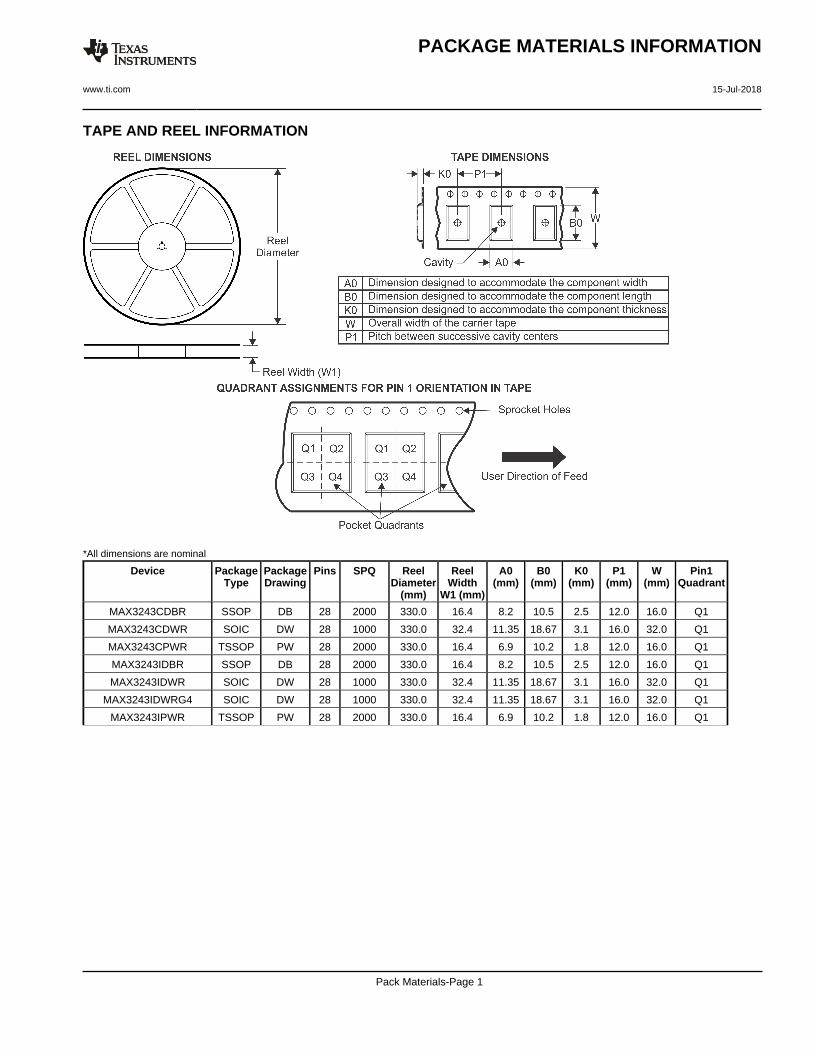
TAPE AND REEL INFORMATION
*All dimensions are nominal
Device PackageType
PackageDrawing
Pins SPQ ReelDiameter
(mm)
ReelWidth
W1 (mm)
A0(mm)
B0(mm)
K0(mm)
P1(mm)
W(mm)
Pin1Quadrant
MAX3243CDBR SSOP DB 28 2000 330.0 16.4 8.2 10.5 2.5 12.0 16.0 Q1
MAX3243CDWR SOIC DW 28 1000 330.0 32.4 11.35 18.67 3.1 16.0 32.0 Q1
MAX3243CPWR TSSOP PW 28 2000 330.0 16.4 6.9 10.2 1.8 12.0 16.0 Q1
MAX3243IDBR SSOP DB 28 2000 330.0 16.4 8.2 10.5 2.5 12.0 16.0 Q1
MAX3243IDWR SOIC DW 28 1000 330.0 32.4 11.35 18.67 3.1 16.0 32.0 Q1
MAX3243IDWRG4 SOIC DW 28 1000 330.0 32.4 11.35 18.67 3.1 16.0 32.0 Q1
MAX3243IPWR TSSOP PW 28 2000 330.0 16.4 6.9 10.2 1.8 12.0 16.0 Q1
PACKAGE MATERIALS INFORMATION
www.ti.com 15-Jul-2018
Pack Materials-Page 1
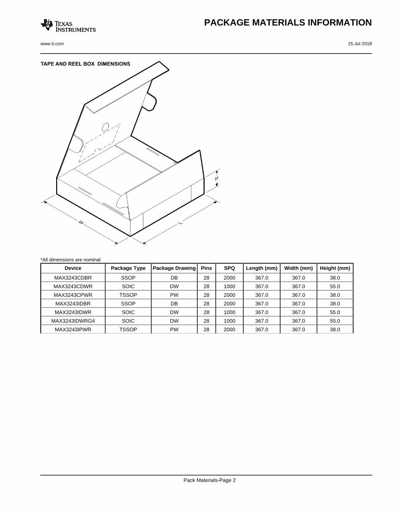
*All dimensions are nominal
Device Package Type Package Drawing Pins SPQ Length (mm) Width (mm) Height (mm)
MAX3243CDBR SSOP DB 28 2000 367.0 367.0 38.0
MAX3243CDWR SOIC DW 28 1000 367.0 367.0 55.0
MAX3243CPWR TSSOP PW 28 2000 367.0 367.0 38.0
MAX3243IDBR SSOP DB 28 2000 367.0 367.0 38.0
MAX3243IDWR SOIC DW 28 1000 367.0 367.0 55.0
MAX3243IDWRG4 SOIC DW 28 1000 367.0 367.0 55.0
MAX3243IPWR TSSOP PW 28 2000 367.0 367.0 38.0
PACKAGE MATERIALS INFORMATION
www.ti.com 15-Jul-2018
Pack Materials-Page 2
www.ti.com
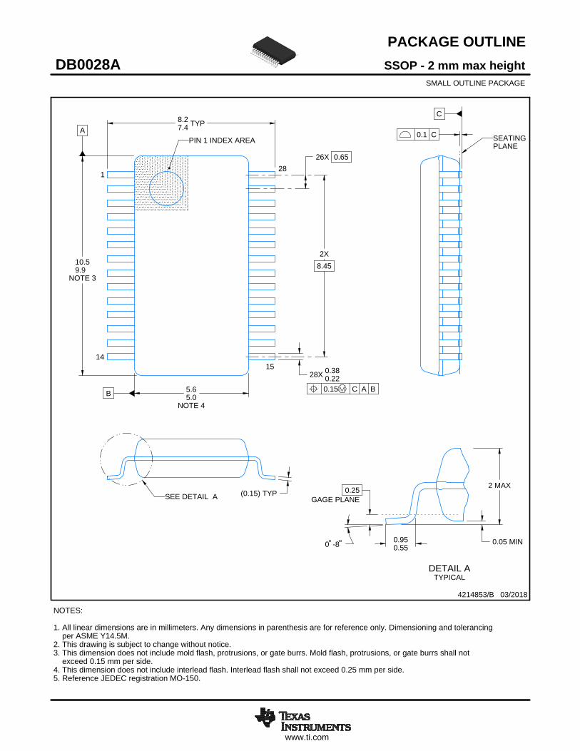
PACKAGE OUTLINE
C
26X 0.65
2X8.45
28X 0.380.22
8.27.4 TYP
SEATINGPLANE
0.05 MIN
0.25GAGE PLANE
0 -8
2 MAX
B 5.65.0
NOTE 4
A
10.59.9
NOTE 3
0.950.55
(0.15) TYP
SSOP - 2 mm max heightDB0028ASMALL OUTLINE PACKAGE
4214853/B 03/2018
1
1415
28
0.15 C A B
PIN 1 INDEX AREA
SEE DETAIL A
0.1 C
NOTES: 1. All linear dimensions are in millimeters. Any dimensions in parenthesis are for reference only. Dimensioning and tolerancing per ASME Y14.5M. 2. This drawing is subject to change without notice. 3. This dimension does not include mold flash, protrusions, or gate burrs. Mold flash, protrusions, or gate burrs shall not exceed 0.15 mm per side. 4. This dimension does not include interlead flash. Interlead flash shall not exceed 0.25 mm per side.5. Reference JEDEC registration MO-150.
A 15DETAIL ATYPICAL
SCALE 1.500
www.ti.com
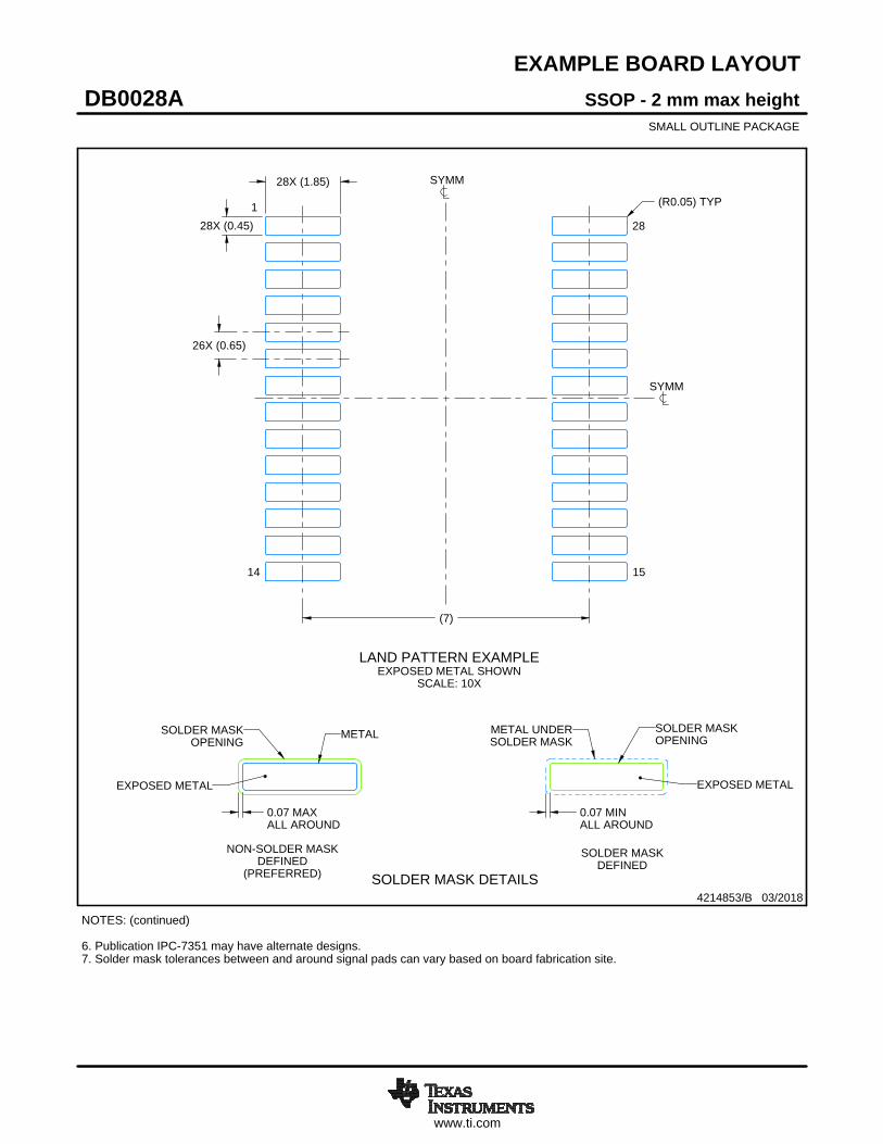
EXAMPLE BOARD LAYOUT
0.07 MAXALL AROUND
0.07 MINALL AROUND
28X (1.85)
28X (0.45)
26X (0.65)
(7)
(R0.05) TYP
SSOP - 2 mm max heightDB0028ASMALL OUTLINE PACKAGE
4214853/B 03/2018
NOTES: (continued) 6. Publication IPC-7351 may have alternate designs. 7. Solder mask tolerances between and around signal pads can vary based on board fabrication site.
LAND PATTERN EXAMPLEEXPOSED METAL SHOWN
SCALE: 10X
SYMM
SYMM
1
14 15
28
15.000
METALSOLDER MASKOPENING
METAL UNDERSOLDER MASK
SOLDER MASKOPENING
EXPOSED METALEXPOSED METAL
SOLDER MASK DETAILS
NON-SOLDER MASKDEFINED
(PREFERRED)
SOLDER MASKDEFINED
www.ti.com
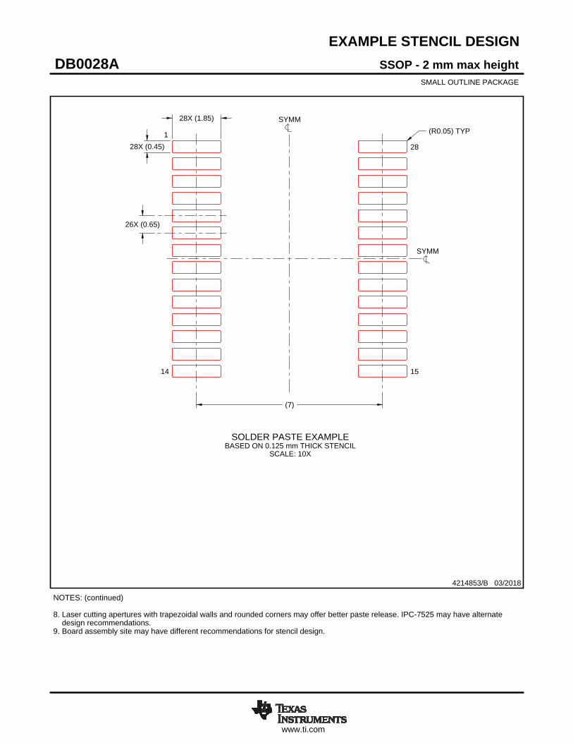
EXAMPLE STENCIL DESIGN
28X (1.85)
28X (0.45)
26X (0.65)
(7)
(R0.05) TYP
SSOP - 2 mm max heightDB0028ASMALL OUTLINE PACKAGE
4214853/B 03/2018
NOTES: (continued) 8. Laser cutting apertures with trapezoidal walls and rounded corners may offer better paste release. IPC-7525 may have alternate design recommendations. 9. Board assembly site may have different recommendations for stencil design.
SOLDER PASTE EXAMPLEBASED ON 0.125 mm THICK STENCIL
SCALE: 10X
SYMM
SYMM
1
14 15
28
IMPORTANT NOTICE
Texas Instruments Incorporated (TI) reserves the right to make corrections, enhancements, improvements and other changes to itssemiconductor products and services per JESD46, latest issue, and to discontinue any product or service per JESD48, latest issue. Buyersshould obtain the latest relevant information before placing orders and should verify that such information is current and complete.TI’s published terms of sale for semiconductor products (http://www.ti.com/sc/docs/stdterms.htm) apply to the sale of packaged integratedcircuit products that TI has qualified and released to market. Additional terms may apply to the use or sale of other types of TI products andservices.Reproduction of significant portions of TI information in TI data sheets is permissible only if reproduction is without alteration and isaccompanied by all associated warranties, conditions, limitations, and notices. TI is not responsible or liable for such reproduceddocumentation. Information of third parties may be subject to additional restrictions. Resale of TI products or services with statementsdifferent from or beyond the parameters stated by TI for that product or service voids all express and any implied warranties for theassociated TI product or service and is an unfair and deceptive business practice. TI is not responsible or liable for any such statements.Buyers and others who are developing systems that incorporate TI products (collectively, “Designers”) understand and agree that Designersremain responsible for using their independent analysis, evaluation and judgment in designing their applications and that Designers havefull and exclusive responsibility to assure the safety of Designers' applications and compliance of their applications (and of all TI productsused in or for Designers’ applications) with all applicable regulations, laws and other applicable requirements. Designer represents that, withrespect to their applications, Designer has all the necessary expertise to create and implement safeguards that (1) anticipate dangerousconsequences of failures, (2) monitor failures and their consequences, and (3) lessen the likelihood of failures that might cause harm andtake appropriate actions. Designer agrees that prior to using or distributing any applications that include TI products, Designer willthoroughly test such applications and the functionality of such TI products as used in such applications.TI’s provision of technical, application or other design advice, quality characterization, reliability data or other services or information,including, but not limited to, reference designs and materials relating to evaluation modules, (collectively, “TI Resources”) are intended toassist designers who are developing applications that incorporate TI products; by downloading, accessing or using TI Resources in anyway, Designer (individually or, if Designer is acting on behalf of a company, Designer’s company) agrees to use any particular TI Resourcesolely for this purpose and subject to the terms of this Notice.TI’s provision of TI Resources does not expand or otherwise alter TI’s applicable published warranties or warranty disclaimers for TIproducts, and no additional obligations or liabilities arise from TI providing such TI Resources. TI reserves the right to make corrections,enhancements, improvements and other changes to its TI Resources. TI has not conducted any testing other than that specificallydescribed in the published documentation for a particular TI Resource.Designer is authorized to use, copy and modify any individual TI Resource only in connection with the development of applications thatinclude the TI product(s) identified in such TI Resource. NO OTHER LICENSE, EXPRESS OR IMPLIED, BY ESTOPPEL OR OTHERWISETO ANY OTHER TI INTELLECTUAL PROPERTY RIGHT, AND NO LICENSE TO ANY TECHNOLOGY OR INTELLECTUAL PROPERTYRIGHT OF TI OR ANY THIRD PARTY IS GRANTED HEREIN, including but not limited to any patent right, copyright, mask work right, orother intellectual property right relating to any combination, machine, or process in which TI products or services are used. Informationregarding or referencing third-party products or services does not constitute a license to use such products or services, or a warranty orendorsement thereof. Use of TI Resources may require a license from a third party under the patents or other intellectual property of thethird party, or a license from TI under the patents or other intellectual property of TI.TI RESOURCES ARE PROVIDED “AS IS” AND WITH ALL FAULTS. TI DISCLAIMS ALL OTHER WARRANTIES ORREPRESENTATIONS, EXPRESS OR IMPLIED, REGARDING RESOURCES OR USE THEREOF, INCLUDING BUT NOT LIMITED TOACCURACY OR COMPLETENESS, TITLE, ANY EPIDEMIC FAILURE WARRANTY AND ANY IMPLIED WARRANTIES OFMERCHANTABILITY, FITNESS FOR A PARTICULAR PURPOSE, AND NON-INFRINGEMENT OF ANY THIRD PARTY INTELLECTUALPROPERTY RIGHTS. TI SHALL NOT BE LIABLE FOR AND SHALL NOT DEFEND OR INDEMNIFY DESIGNER AGAINST ANY CLAIM,INCLUDING BUT NOT LIMITED TO ANY INFRINGEMENT CLAIM THAT RELATES TO OR IS BASED ON ANY COMBINATION OFPRODUCTS EVEN IF DESCRIBED IN TI RESOURCES OR OTHERWISE. IN NO EVENT SHALL TI BE LIABLE FOR ANY ACTUAL,DIRECT, SPECIAL, COLLATERAL, INDIRECT, PUNITIVE, INCIDENTAL, CONSEQUENTIAL OR EXEMPLARY DAMAGES INCONNECTION WITH OR ARISING OUT OF TI RESOURCES OR USE THEREOF, AND REGARDLESS OF WHETHER TI HAS BEENADVISED OF THE POSSIBILITY OF SUCH DAMAGES.Unless TI has explicitly designated an individual product as meeting the requirements of a particular industry standard (e.g., ISO/TS 16949and ISO 26262), TI is not responsible for any failure to meet such industry standard requirements.Where TI specifically promotes products as facilitating functional safety or as compliant with industry functional safety standards, suchproducts are intended to help enable customers to design and create their own applications that meet applicable functional safety standardsand requirements. Using products in an application does not by itself establish any safety features in the application. Designers mustensure compliance with safety-related requirements and standards applicable to their applications. Designer may not use any TI products inlife-critical medical equipment unless authorized officers of the parties have executed a special contract specifically governing such use.Life-critical medical equipment is medical equipment where failure of such equipment would cause serious bodily injury or death (e.g., lifesupport, pacemakers, defibrillators, heart pumps, neurostimulators, and implantables). Such equipment includes, without limitation, allmedical devices identified by the U.S. Food and Drug Administration as Class III devices and equivalent classifications outside the U.S.TI may expressly designate certain products as completing a particular qualification (e.g., Q100, Military Grade, or Enhanced Product).Designers agree that it has the necessary expertise to select the product with the appropriate qualification designation for their applicationsand that proper product selection is at Designers’ own risk. Designers are solely responsible for compliance with all legal and regulatoryrequirements in connection with such selection.Designer will fully indemnify TI and its representatives against any damages, costs, losses, and/or liabilities arising out of Designer’s non-compliance with the terms and provisions of this Notice.
Mailing Address: Texas Instruments, Post Office Box 655303, Dallas, Texas 75265Copyright © 2018, Texas Instruments Incorporated


![MAX3221 3-V to 5.5-V RS-232 Line Driver and Receiver … TX POWER APD EN [RX] DIN ROUT DOUT RS232 RIN RS232 1 1 1 1 FORCEON FORCEOFF INVALID STATUS 3.3 V, 5 V Product Folder Sample](https://static.fdocuments.us/doc/165x107/5ae2df1f7f8b9a495c8c8d92/max3221-3-v-to-55-v-rs-232-line-driver-and-receiver-tx-power-apd-en-rx-din.jpg)