Facilities at the Nuclear Physics Institute Academy of Sciences of the Czech Rep. , Řež
Upload
samuel-horwichCategory
view
214download
0
DESY Zeuthen - Technical seminar - 23.10.2012
1
ALICE ITS Upgrade Projectand
Contribution of NPI in ŘežJozef Ferencei
Nuclear Physics InstituteCzech Academy of Sciences
Řež

DESY Zeuthen - Technical seminar - 23.10.2012
2
Outline:- ALICE detector with present Inner Tracker
System (ITS)- ITS upgrade
- design goals, milestones, options, technologies, timelines
- NPI cyclotron U-120M as a test bed- available beams, open access mode
- Single Upset Event- history, design factors, critical charge
- Contribution of Nuclear Physics Institute NPI- measurement setup, calibration run, plans

DESY Zeuthen - Technical seminar - 23.10.2012
3
A Large Ion Collider ExperimentCentral Detectors: Inner Tracking System (ITS) Time Projection Chamber (TPC) Transition Radiation Detector (TRD) Time-of-Flight (TOF) High Momentum PID (HMPID) Spectrometers: Photon Multiplicity Forward Multiplicity Muon SpectrometerCalorimeters: EM Calorimeter (EMCAL) Photon Spectrometer (PHOS)Zero Degree Calorimeter (ZDC)
Detector:Length: 26 metersHeight: 16 metersWeight: 10,000 tons
Collaboration:> 1000 Members> 100 Institutes > 30 countries
Ultra-relativistic nucleus-nucleus collisions- study behavior of strongly interacting matter under
extreme conditions of compression and heatProton-Proton collisions
- reference data for heavy-ion program- unique physics (momentum cutoff < 100 MeV/c,
excellent PID, efficient minimum bias trigger)

DESY Zeuthen - Technical seminar - 23.10.2012
4
ALICE ITS (Inner Tracking System) - current detector
Current ITS consists of 6 concentricbarrels of silicon detectors
3 different technologies:• 2 layers of silicon pixel (SPD)• 2 layers of silicon drift (SDD)• 2 layers of silicon strips (SSD)
Layer/ Type Radius[cm]
Length[cm]
Number ofmodules
Active area per module [mm2]
Nom. resolutionrΦ x z [µm]
Material budgetX/X0 [%]
Beam pipe 2.94 - - - - 0.22
1 / Pixel 3.9 28.2 80 12.8 × 70.7 12 × 100 1.14
2 / Pixel 7.6 28.2 160 12.8 × 70.7 12 × 100 1.14
Thermal Shield 11.5 - - - - 0.65
3 / Drift 15.0 44.4 84 70.2 x 75.3 35 × 25 1.13
4 / Drift 23.9 59.4 176 70.2 x 75.3 35 × 25 1.26
Thermal Shield 31.0 - - - - 0.65
5 / Strip 38.0 86.2 748 73.0 x x40.0 30 × 830 0.83
6 / Strip 43.0 97.8 950 73.0 x x40.0 20 × 830 0.83

DESY Zeuthen - Technical seminar - 23.10.2012
5
ITS Upgrade Design Goals1. Improve impact parameter resolution by a factor of ~3:• Get closer to IP (position of 1-st layer): 39 mm →22 mm • Reduce material budget: X/X0 /layer: ~1.14% → ~ 0.3%• Reduce pixel size (currently 50 µm x 425 µm):
monolithic pixels → O(20 µm x 20 µm), hybrid pixels → state-of-the-art O(50 µm x 50 µm)
2. Improve tracking efficiency and pT resolution at low pT:• Increase granularity: 6 layers → 7 layers , reduce pixel size• Increase radial extension: 39-430 mm → 22– 430(500) mm3. Fast readout: readout of PbPb interactions at > 50 kHz and pp interactions at several MHz4. Fast insertion/removal for yearly maintenance: possibility to replace non functioning detector modules
during yearly shutdown

DESY Zeuthen - Technical seminar - 23.10.2012
6
ITS Upgrade Design MilestonesMarch 2012Upgrade Strategy for ALICE at High Rate, CERN-LHCC–2012-005Upgrade of the Inner Tracking System, CDR0, CERN-LHCC-2012-004
September 2012Comprehensive Letter of Intent submitted to LHCC →Upgrade of the ALICE Experiment, Letter of Intent, CERN–LHCC–2012 -12https://cdsweb.cern.ch/record/1475243/files/LHCC-I-022.pdftogether with:Upgrade of the Inner Tracking System, CDR1, CERN-LHCC–2012-13https://cdsweb.cern.ch/record/1475244/files/LHCC-P-005.pdf
Aim for 2013 →TDR

DESY Zeuthen - Technical seminar - 23.10.2012
7
Option A: 7 layers of pixel detectors better standalone tracking efficiency and momentum resolution worse particle identificationOption B: 3 inner layers of pixel detectors and 4 outer layers of strip detectors worse standalone tracking efficiency and momentum resolution better particle identification
Upgrade options
Option AOption B
7 layers of pixels
3 layers of pixels
4 layers of strips
Pixels: O( 20x20µm2 – 50 x 50µm2)Strips: 95 µm x 2 cm, double sided
Pixels: O(20x20µm2 – 50 x 50µm2)

DESY Zeuthen - Technical seminar - 23.10.2012
8
Parameter Design Value CommentMaterial Budget per Layer 0.3% X0 Max.: 0.5% X0
Chip Size 15 mm x 30 mm Target Size
Pixel Size (r-Φ) 20 µm Max.: 30 µm
Pixel Size (z) 20 µm Max.: 50 µm
Readout Time ≤ 30 µs Max.: 50 µs
Power Density 0.3 W/cm2 Max.: 0.5 W/cm2
Hit Density 150 hits/cm2 Peak Value
Radiation Levels(Layer 1, r=22 mm)
700 krad (TID)1 x 10¹³ neq/cm2 (NIEL)
Safety-factor: 4
Technical specifications for the inner layers (layers 1-3) of ITS upgrade

DESY Zeuthen - Technical seminar - 23.10.2012
9
Technical specifications for the outer layers (layers 4-7) of ITS upgrade
Parameter Design Value Comment
Material Budget per Layer 0.3% X0 Max.: 0.8% X0
Cell Size (r-Φ) ≤ 70 µm
Cell Size (z) ≤ 2 cm
Readout Time ≤ 30 µs Max.: 50 µs
Power Density 0.3 W/cm2 Max.: 0.5 W/cm2
Hit Density ≈ 1 hit/cm2 Layer 4
Radiation Levels(Layer 4, r=200 mm)
10 krad (TID)3 x 10¹¹ neq/cm2 (NIEL)
Safety-factor: 4

DESY Zeuthen - Technical seminar - 23.10.2012
10
Improved impact parameter resolution and high standalone tracking efficiency
Large on-going MC simulation effort using detailed GEANT
simulation within ALICE standard framework AliRoot
DESY Zeuthen - Technical seminar - 23.10.2012
11
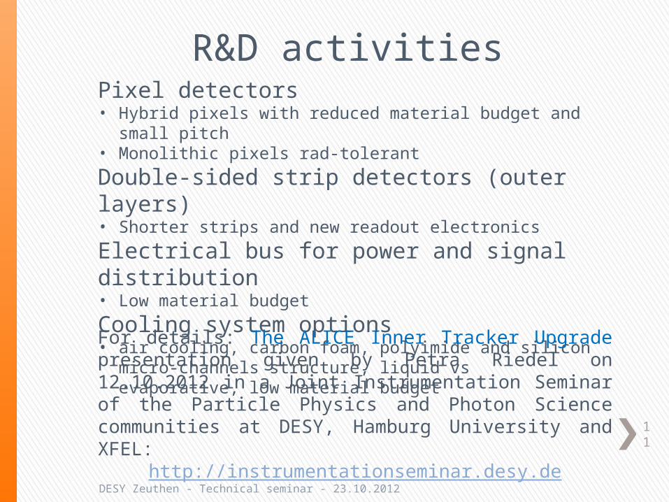
Pixel detectors• Hybrid pixels with reduced material budget and small pitch• Monolithic pixels rad-tolerant
Double-sided strip detectors (outer layers)• Shorter strips and new readout electronics
Electrical bus for power and signal distribution• Low material budget
Cooling system options• air cooling, carbon foam, polyimide and silicon micro-channels
structure, liquid vs evaporative, low material budget
R&D activities
For details: The ALICE Inner Tracker Upgrade presentation given by Petra Riedel on 12.10.2012 in a Joint Instrumentation Seminar of the Particle Physics and Photon Science communities at DESY, Hamburg University and XFEL:
http://instrumentationseminar.desy.de

DESY Zeuthen - Technical seminar - 23.10.2012
12
Monolithic Pixel technology
Features: Made significant progress, soon to be installed in STAR All-in-one, detector-connection-readout Sensing layer included in the CMOS chip Charge collection mostly by diffusion (Monolithic Active Pixel Sensors
- MAPS), but some development based on charge collection by drift Small pixel size: 20 µm x 20 µm target size Small material budget: 0.3% X0 per layer
Options under study: MIMOSA (←STAR-PXL) like in 180 nm
CMOS →TowerJazz INMAPS in 180 nm CMOS →TowerJazz LePix in 90 nm CMOS → IBM MISTRAL (←MIMOSA) prototype
circuit (IPHC)
Comparison with hybrid technology:+ material budget+ granularity+ low production cost- radiation tolerance

DESY Zeuthen - Technical seminar - 23.10.2012
13
Hybrid pixel detectors
Well known technology Proven radiation
hardness Pixel size is limited due
to the bump bondingTwo Si-chips limit the
minimal material budget.
High production cost due to the bump bonding
Simplified view → Sandwich:• Sensor• Frontend-readout chip• Interconnect (bump bonds)
Sensor and chip can be optimized separately

DESY Zeuthen - Technical seminar - 23.10.2012
14
Hybrid pixel detectors R&D ongoing: • Bump bonding with 30 μm pitch. • Sensor and readout chip thinning: 50 μm (readout)
+ 100 μm (sensor) = 150 μm in 130 nm CMOS → studies in CERN.
Comparison with monolithic technology:+ radiation tolerance+/- granularity- material budget

DESY Zeuthen - Technical seminar - 23.10.2012
15
Well known technology Provides ionization energy loss
information that is needed for PID Granularity is adequate for the external
layers only
R&D Ongoing: Sensor is based on the old design with
2x shorter strips New readout ASIC will have ADC on-board
Strip Detectors

DESY Zeuthen - Technical seminar - 23.10.2012
16
Timeline of the ITS upgrade project
2012 Finalization of specifications / first prototypes / radiation tests
2013 Selection of technologies and design of mechanics and services
2014 Final Design and validation
2015-2016 Production /construction and test of detector modules
2017 Assembly and pre-commissioning
2018 Installation in ALICE
DESY Zeuthen - Technical seminar - 23.10.2012
17
U-120M cyclotronin Nuclear Physics
Institute Řež as a test bed instrument

DESY Zeuthen - Technical seminar - 23.10.2012
18
protons: 18-38 MeV (15 μA) deuterons: 11-18 MeV (10 μA)
protons: 18-24 MeV (3 μA) deuterons: 11-17 MeV (3 μA) 3He-ions: 20-40 MeV (2 μA)
Activation & Irradiation experimentsPharmaceutical radionuclide production
Spectrometry experiments
High-power neutron target station
Cyclotron U-120M

19
DESY Zeuthen - Technical seminar - 23.10.2012
Acceleration of H- ions and extraction using the stripping foil
Negative mode:Acceleration of H with loosely bounded additional electron → H-
Carbon stripping foil: H- → protonsCarbon foil source of additional neutron background Transmission efficiency (source to extracted beam) typical: 52% for H-

DESY Zeuthen - Technical seminar - 23.10.2012
20
Center of Accelerators and Nuclear Analytical Methods (CANAM infrastructure) offers scientists a unique experimental infrastructure in
nuclear physics and neutron science: http://canam.ujf.cas.cz/
Funded by the Ministry of Education, Youth and Sports of the Czech Republic and Nuclear Physics Institute of the ASCR, experimental facilities are proffered to the users in Open Access mode. The proposals should be submitted via User Portal
Open Access mode

DESY Zeuthen - Technical seminar - 23.10.2012
21
Radiation Hardness -
Single Upset Event

DESY Zeuthen - Technical seminar - 23.10.2012
22
Wikipedia: Change of state in memory cells or registers caused by ionizing particles. The state change is a result of the free charge created by ionization in a sensitive node of the circuit. The SEU itself is not permanently damaging to the transistor's or circuits' functionality.
For some of your infamous Windows blue screen you should blame not only MicroSoft
Single Event Upset
Specific design factors which impact error rates: Increased complexity raises the error rate. Higher-density (higher-capacity) chips are more likely to have errors. Lower-voltage devices are more likely to have errors. Higher speeds (lower latencies) contribute to higher error rates. Lower cell capacitance (less stored charge) causes higher error rates. Shorter bit-lines result in fewer errors. Wafer thinning improves error tolerance (especially with backside contacts). “Radiation hardening” can decrease error rates by several orders of
magnitude , but these techniques cost more, reduce performance, use more power, and/or increase area.

DESY Zeuthen - Technical seminar - 23.10.2012
23
(*) Semico Research Corporations, “Gate Arrays Wane while Standard Cells Soar: ASIC Market Evolution Continues”
Chart (*) includes α particle effects as well as neutron effects.At ground level, cosmic radiation is about 95% neutrons and 5% protons.
Soft Error Rates as a Function of IC Process Technology
History: ground nuclear testing (1954-1957), space electronics (during the 1960s), first evidence of soft errors from α particles in packaging materials (1979) and from sea level cosmics rays. Many resources, e.g.:
http://radhome.gsfc.nasa.gov/radhome/see.htmhttp://www.altera.com/support/devices/reliability/seu/seu-index.html

DESY Zeuthen - Technical seminar - 23.10.2012
24
Charge deposition by ionizing particle can lead to a change in state of a transistor:- Critical charge Qcrit = (0.0023 pC/μm2) L2 ← empirical law
L = feature size (SEU chip: L=0.18 μm)- Energy deposition Edep = LET ρ s
LET = linear energy transfer (energy depositedper unit path length as an energetic particletravels through a material)ρ = density (Si: ρ = 2.33 g/cm3);smax= path length (smax
2 = 2L2 + c2 , for a=b=L, c = device depth)
smin = minimum distance particle of given LET must travel before being able to deposit sufficient energy to cause an SEU.
Particles incident at an angle have a path that is 1/cos(Θ) longer than the path at normal incidence → cosine law.
Single Event Upset

DESY Zeuthen - Technical seminar - 23.10.2012
25
- Charge deposition Qdep = Edep q / wehp
q = 1.6022x10⁻¹⁹ Coulombs/ewehp = electron-hole pair creation energy (Si: wehp = 3.6 eV)
- Minimum LET to cause an upset:LETthreshold = Qcrit wehp / (q smax)
- LETthreshold (APEX FPGA) ≈ 100 keV/mg/cm2
- LET (30 MeV proton in Si) = 15 keV/mg/cm2
Single Event Upset
Even using a relatively conservative error rate a system with 1 GByte of RAM can expect an error every two weeks due to cosmics rays. A hypothetical Terabyte system would experience a soft error every few minutes.
The most commonly used system of error recovery (Error Checking and Correction - ECC), adds extra bits (check bits) to each data item. These bits are re-computed and compared whenever the data item is accessed. Most ECC algorithms can correct single-bit errors and detect, but not correct, double-bit errors.
DESY Zeuthen - Technical seminar - 23.10.2012
26
Contribution into ITS upgrade projectof NPI CAS Řež
and IEP SAS KošiceGroup consisting of
NPI CAS: V.Kushpil, S.Kushpil, V.Mikhaylov, J.F.IEP SAS: J.Špalek

DESY Zeuthen - Technical seminar - 23.10.2012
27
SEU chip
Contribution of our group: to measure the SEU sensitivity / cross section for: • single port RAMs (16 x 1024x16bits) • dual port RAMs (8 x 2048x16bits) • 16 bit 32K stages shift register
Circuits designed in CERN using a commercial 180 nm low power CMOS technology:- TowerJazz 0.18 mm- 1.8 V- 4 Metal Layers- Max. frequency 10MHz
SEU cross section per bit:
σseu =
Estimated SEU cross section per bit: ≈ 10-13 cm2 bit-1

DESY Zeuthen - Technical seminar - 23.10.2012
28
SEU chip bonding in DESY ZeuthenMany thanks to
Wolfgang Lange and Jürgen Pieper
SEU chip
Custom SEU chip boardby V.Kushpil

DESY Zeuthen - Technical seminar - 23.10.2012
29
S. Kushpil, V.Mikhaylov
Graphical User Interface (LabView)
Custom analog signals DAQ Board
SEU chip readout via FPGA with clock speed
or USB (slower)
V. Kushpil
Measurement setup

DESY Zeuthen - Technical seminar - 23.10.2012
30
Measurement setup schematics
V.Mikhaylov
Neutron background ≈10 mSv/h
Neutron background
≈1 mSv/h
Position Control System MCL-2
from LANG GmbH & Co. KG Hüttenberg
UNIDOS system with ionization chamber from PTW Freiburg

DESY Zeuthen - Technical seminar - 23.10.2012
31
Measurement setup in cyclotron
X & Y 1µm step motors
2 x AL + 1 x Au activation analysis
foils
Pt100 thermometer
Ionization chamber
5x5 mm2 (= SEU chip) hole

DESY Zeuthen - Technical seminar - 23.10.2012
32
Proton beam profile scan in negative mode
Low intensity scan:σx = 16.8 mm and σy = 19.3 mm
High intensity scanσx = 19.4 mm and σy = 20.9 mm
Irradiation homogeneity required better than 10% →
beam alignment at the level of few mm for SEU chip 5 x 5 mm2
5 mm
Low intensity (~0.4 µA): with collimator slit 1 mmHigh intensity (~2.1 µA):
with collimator fully open
Extracted Ep = 27.845 MeV
→ Radiation doses ~ 1 Mrad (10 kGray) can be accumulated within short time

DESY Zeuthen - Technical seminar - 23.10.2012
33
Immediate plans:
- finish & test the electronics setup- determine SEU proton energy dependence as
a function of accumulated doses- verify SEU proton angular dependence- especially look for multiple bit errors- the same above also for neutrons
Thank you for your attention !