1 DESIGN OF 4-BIT ALU Fairchild Semiconductor DM74LS181 Prashanth Kommuri Akram Khan Gopinath...
23
1 DESIGN OF 4-BIT ALU Fairchild Semiconductor DM74LS181 Prashanth Kommuri Akram Khan Gopinath Akkinepally Advisor: Dr. David W. Parent 5 December 2005
-
date post
20-Dec-2015 -
Category
Documents
-
view
213 -
download
0
Transcript of 1 DESIGN OF 4-BIT ALU Fairchild Semiconductor DM74LS181 Prashanth Kommuri Akram Khan Gopinath...

1
DESIGN OF 4-BIT ALUFairchild Semiconductor DM74LS181
Prashanth KommuriAkram Khan
Gopinath Akkinepally
Advisor: Dr. David W. Parent5 December 2005
2
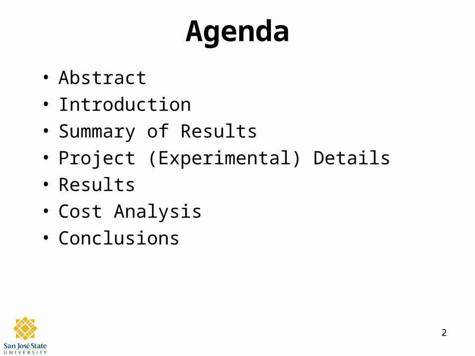
Agenda
• Abstract• Introduction• Summary of Results• Project (Experimental) Details• Results• Cost Analysis• Conclusions

3
Abstract
• The Aim of the project is to design a 4-bit ALU to perform 16 arithmetic and logic operations.
• The circuit is designed so as to meet the following specifications: – Frequency: 200 MHz.– Power : 50 mW. – Area : 500x500 µm2
• The results are verified with AMI06 technology, Cadence tools.

4
Introduction
Why this project?
• The ALU is a fundamental building block of any computing system.
• Challenging to design a 15 logic level design using CMOS Technology.
• Design consists of different kinds of logic… Ripple Carry Adder, Subtractor, DFF, Mux, Inv, Nand, Nor, Xor, etc.

5
ALU Block Diagram

6
Function Table
A, B = 4 Bit Input, M , S0, S1,S2, S3 = Status Control Pin
Cn = Carry in

7
Project Summary
• The ALU performs 16 Arithmetic functions and 16 Logical functions at 250MHz.
• Uses Ripple carry adder to perform addition.
• Design uses maximum power of 19.48mW
• Maximum area is 468 x 349µm2
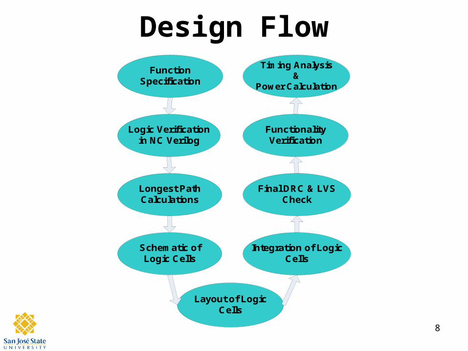
8
Design FlowFunction
Specification
Logic Verification in NC Verilog
Longest Path Calculations
Schematic of Logic Cells
Layout of Logic Cells
Integration of Logic Cells
Functionality Verification
Timing Analysis &
Power Calculation
Final DRC & LVS Check

9
Gate Level Diagram

10
Longest Path

11
Longest Path Calculations
Total Propagation delay for the longest path = 2.97ns
LOGIC LEVEL GATE CINT CG TO DRIVE PHL NSN NSP N M R WN WP
F F s cm cm
1 INV 5.00E-15 3.5000E-14 1.00E-10 1 1 1 1 1.805 3.88E-04 7.00E-04
2 NOR2 5.00E-15 2.3248E-14 2.00E-10 1 2 2 3 3.560 1.96E-04 4.50E-04
3 NAND2 5.00E-15 1.5841E-14 1.50E-10 2 1 3 2 0.896 4.62E-04 5.49E-04
4 XOR2 5.00E-15 2.1963E-14 4.00E-10 2 2 4 6 1.730 3.12E-04 5.40E-04
5 INV 5.00E-15 1.9291E-14 1.00E-10 1 1 1 1 1.805 2.24E-04 4.05E-04
6 INV 5.00E-15 1.5562E-14 1.00E-10 1 1 1 1 1.805 2.44E-04 3.59E-04
7 NAND2 5.00E-15 1.5120E-14 1.50E-10 2 1 3 2 0.896 4.46E-04 5.31E-04
8 NOR2 5.00E-15 2.1396E-14 2.00E-10 1 2 2 3 3.560 3.19E-04 7.14E-04
9 NOR2 5.00E-15 2.2338E-14 2.20E-10 1 2 2 3 3.550 2.70E-04 5.73E-04
10 NAND3 5.00E-15 1.9140E-14 2.70E-10 3 1 5 3 0.588 7.81E-04 4.59E-04
11 NOR2 2.00E-14 1.8637E-13 5.30E-10 1 2 2 3 3.395 3.36E-04 8.58E-04
12 INV 5.00E-15 2.5029E-14 1.00E-10 1 1 1 1 1.805 3.41E-04 5.38E-04
13 NAND3 5.00E-15 1.9750E-14 2.60E-10 3 1 5 3 0.588 9.38E-04 5.52E-04
14 INV 5.00E-15 5.4998E-14 1.10E-10 1 1 1 1 1.803 5.19E-04 9.35E-04
15 INV 5.00E-15 2.9406E-14 8.00E-11 1 1 1 1 1.810 5.45E-04 9.08E-04
Total Delay = 2.97E-09

12
Schematic- Top-Level

13
Simulation 1 (Arithmetic operations)
F = A F= A plus (AB)’
F= minus 1 F= A minus B minus 1
14
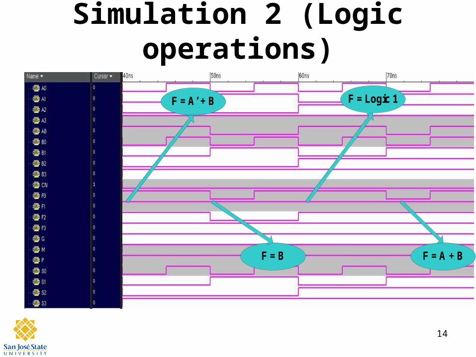
Simulation 2 (Logic operations)
F = A’ + B F = Logic 1
F = B F = A + B

15
Layout

16
Verification
DRC Results
NETLISTS MATCH

17
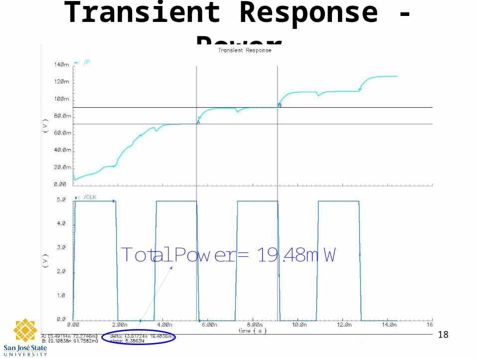
Transient Response
A=1010 B=0101 S=1011 M=1 F = 0000 , F= A B
18
Transient Response -Power
Total Power = 19.48mW

19
Results
• The ALU performs all 32 functions at a 250MHz clock and a load of 30fF.
• Power dissipation is 19.48mW.
• Area of the layout is 468 x 349µm2

20
Cost Analysis• Time is money !• Time spent on each phase is:
Design and Implementation Phase: Logic design and NC Verilog check – 3 days.Transistor level design and simulation – 1 week. Floor planning and Layout – 2 weeks.
Verification and Testing Phase:Post extraction, Power & Timing analysis – 1 day.

21
Conclusions
• Designed a 4-Bit ALU that performs 16 arithmetic and 16 logical functions at 250MHz frequency with setup and hold time 0.6ns, driving up to 30fF.
• This circuit can be used as a building block for 16/32-bit ALU.
• The Logic design can be modified to perform more functions.

22
Lessons Learned
• Cell based design• Uniform cell height• No bends in the poly• Floor planning• Grid pattern for Vdd and gnd• Debugging LVS errors using extracted view

23
Acknowledgements
• Thanks to our parents for their support.
• Thanks to Professor David W. Parent for his guidance.
• Thanks to Cadence Design Systems for the VLSI lab