
1 ASIC DESIGN Asim J. Al-Khalili---Concordia University.
115
C O N C O R DIA VLSI D E SIG N LAB 1 ASIC DESIGN Asim J. Al-Khalili---Concordia University
-
Upload
sydney-hunt -
Category
Documents
-
view
227 -
download
0
Transcript of 1 ASIC DESIGN Asim J. Al-Khalili---Concordia University.

CONCORDIAVLSI DESIGN LAB
1
ASIC DESIGNAsim J. Al-Khalili---Concordia University

CONCORDIAVLSI DESIGN LAB
2
Objectives •What technologies are there?•Why CMOS?•Where are we?•How far we can go•What is the worldwide view of microelectronics ?
•What are the different implementation methods?
CONCORDIAVLSI DESIGN LAB
3
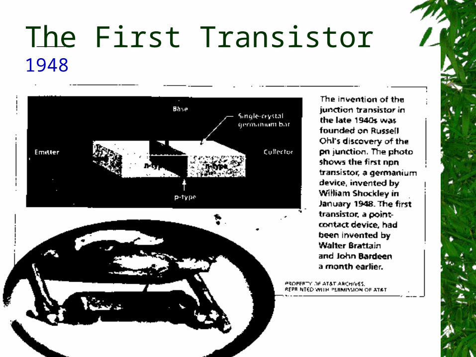
The First Transistor 1948
CONCORDIAVLSI DESIGN LAB
4
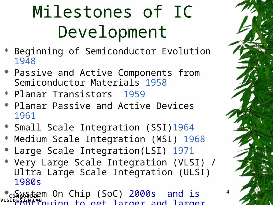
Milestones of IC Development
Beginning of Semiconductor Evolution 1948 Passive and Active Components from
Semiconductor Materials 1958 Planar Transistors 1959 Planar Passive and Active Devices 1961 Small Scale Integration (SSI)1964 Medium Scale Integration (MSI) 1968 Large Scale Integration(LSI) 1971 Very Large Scale Integration (VLSI) / Ultra
Large Scale Integration (ULSI) 1980s System On Chip (SoC) 2000s and is
continuing to get larger and larger
CONCORDIAVLSI DESIGN LAB
5
WORLD OF SILICON
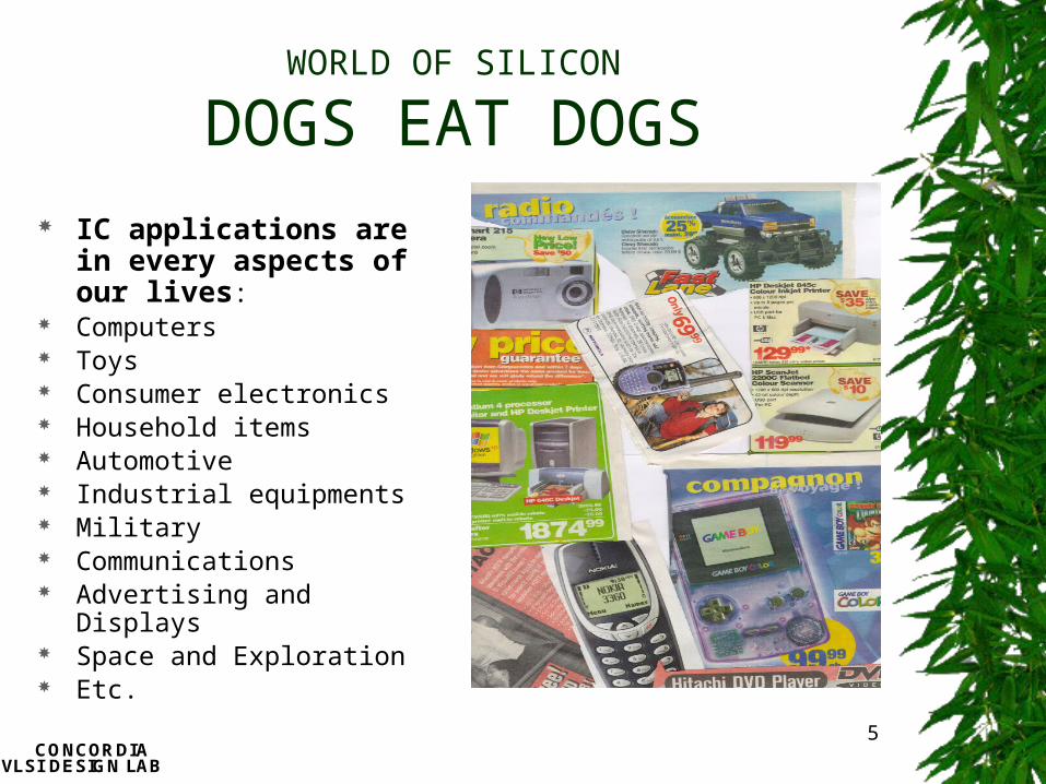
DOGS EAT DOGS IC applications are in
every aspects of our lives:
Computers Toys Consumer electronics Household items Automotive Industrial equipments Military Communications Advertising and Displays Space and Exploration Etc.
CONCORDIAVLSI DESIGN LAB
6
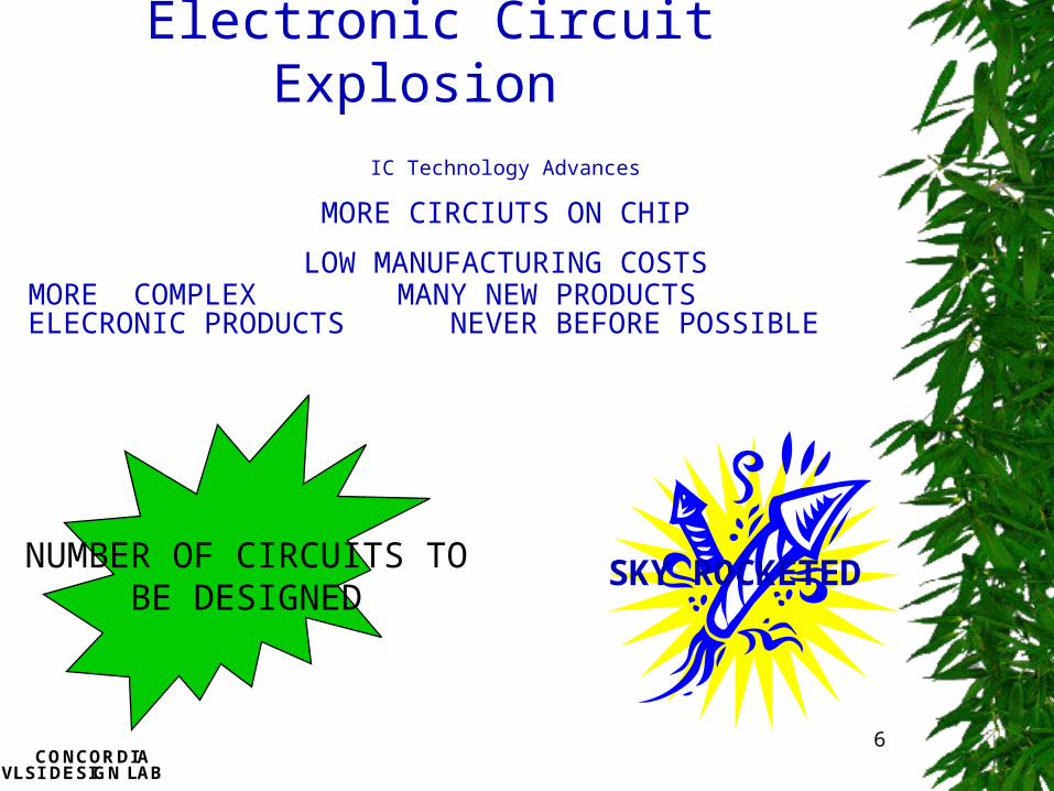
Electronic Circuit Explosion IC Technology Advances
MORE CIRCIUTS ON CHIP
LOW MANUFACTURING COSTSMORE COMPLEX MANY NEW PRODUCTS ELECRONIC PRODUCTS NEVER BEFORE POSSIBLE
NUMBER OF CIRCUITS TO BE DESIGNED
SKY ROCKETED

CONCORDIAVLSI DESIGN LAB
7
Emerging-in-car systems

CONCORDIAVLSI DESIGN LAB
8
The Internet Big Bang

CONCORDIAVLSI DESIGN LAB
EVEN ATMs
9

CONCORDIAVLSI DESIGN LAB
10
The Incredible Shrinking Transistor
1970’s
1980’s 2000 2014

CONCORDIAVLSI DESIGN LAB
11
Reduction in Feature SizePhysical parameter
Constant-Electric FieldScaling Factor
GeneralizedScaling Factor
Generalized SelectiveScaling Factor
Channel length,Insulator thickness 1/ 1/ 1/d
Wiring width,channel width 1/ 1/ 1/w
Electric field indevice
1
Voltage 1/ / /d
On-current perdevice 1/ / /w
Doping d
Area 1/2 1/2 1/w2
Capacitance 1/ 1/ 1/w
Gate delay 1/ 1/ 1/d
Power dissipation 1/2 2/2 2/w
d
Power density 1 2 2w/d
Reduce transistor and wiring by a

CONCORDIAVLSI DESIGN LAB
12
The First Computer
The BabbageDifference Engine(1832)
25,000 partscost: £17,470
©Prentice Hall/Rabaey
Using finite difference it is possible to replace multiplication, division and subtraction by addition, So in calculating the value of a polynomial we may use addition only .Adding two numbers using gearwheels is easier to implement than doing it by multiplication or division.

CONCORDIAVLSI DESIGN LAB
13
ENIAC - The first electronic computer (1946)
Prentice Hall/Rabaey
20,000 Vacuum Tubes, it cost $500,000It could Add, Subtract and store 10-digit decimal numbers in memoryIt weighted 27 tons, had a size of 80 ft* 8.5 ft* 3 ft, and it required a room of 680 ft2Consumed 150KW

BUT NOW, a small cell phone
By the millions, more powerful, more functions, less weight, less power consumption, less heat generation
CONCORDIAVLSI DESIGN LAB
15
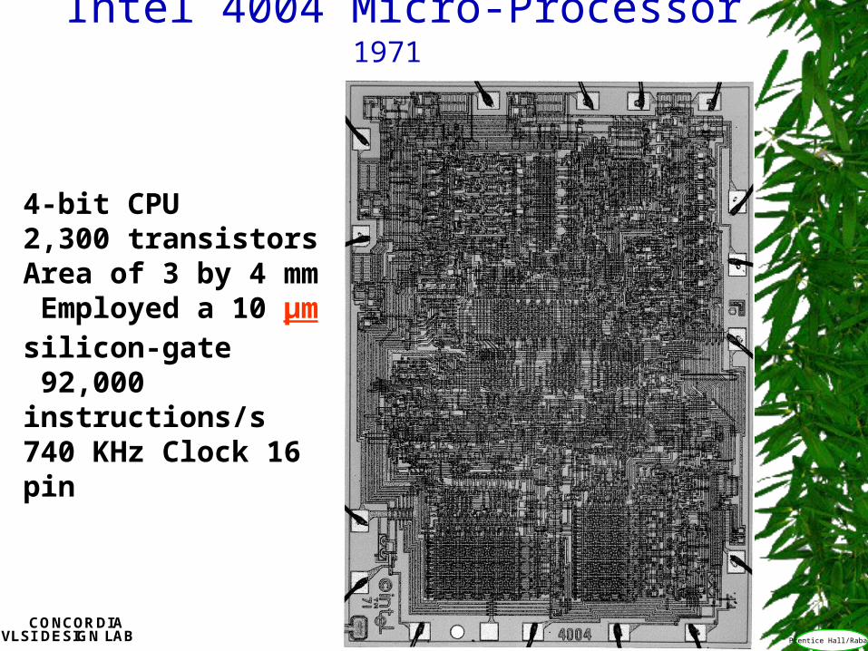
Intel 4004 Micro-Processor 1971
Prentice Hall/Rabaey
4-bit CPU2,300 transistorsArea of 3 by 4 mm Employed a 10 μm silicon-gate 92,000 instructions/s 740 KHz Clock 16 pin

CONCORDIAVLSI DESIGN LAB
16
Intel Pentium (IV) microprocessor 2002
Prentice Hall/Rabaey
A 'Northwood' core Pentium 4 processor (P4A)Northwood core at 2.2 GHz2nd cache 512 KB 55 million transistors, 130 nm Technology

CONCORDIAVLSI DESIGN LAB
17
Number ofLogic Gates
(Moore’s Law)
Logic BlockArea (Moore’s
Law)
Number ofLogic Gates
(Max = 10M)
Logic Block Area(MAX = 10M)
1M 0.909 1M 0.909
2M 0.923 2M 0.923
4M 1.0 4M 1.0
8M 1.091 8M 1.091
24M 1.32 10M 0.55
64M 1.42 10M 0.22
192M 1.782 10M 0.09
Double Logic Gates Every Two Y ears ( Moore’s Law )Maximum Macrocell Size beyond 2005 ( 10 M gates )
1990 2001 20032
2005 2008 2011 2014
100
90
80
70
60
50
40
30
20
10
0
Year
MOORE’S LAW
Intel announces 14 new Ivy Bridge Processors
May. 31, 2012 (8:31 am) By: Matthew Humphries In: Chips, Chips Picks, Geek Pick, News
Intel launched the 22nm Ivy Bridge processors that uses quad-core chips Since then it added another 14 processors to the line-up, only this time the chips are mainly dual-core parts catering to a number of different market segments and platforms. .
Of the 14 new processors, 6 are classed as desktop chips with power use (TDP) ranging from 35-77 watts. These consist mainly of new quad-core chips, but one dual-core desktop chip is also listed (i5-3470T). CPU frequency ranges from 2.6GHz to 2.9GHz and maxing out at 3.4GHz using Intel Turbo Boost on the Core i7 chip. .

IBM Creates New Memory Technology 100 Times Faster Than Flash
by Bryan Vore on July 01, 2011
IBM revealed its new phase-change memory (PCM) tech that could drastically change computing and gaming.IBM says that PCM is able to write and retrieve data 100 times faster than Flash memory. It also lasts much longer, surviving 10 million write cycles compared to the 3,000cycles of Flash that the average consumer can use.IBM claims that PCM will herald a "paradigm shift“ when it hits the market in 2016..
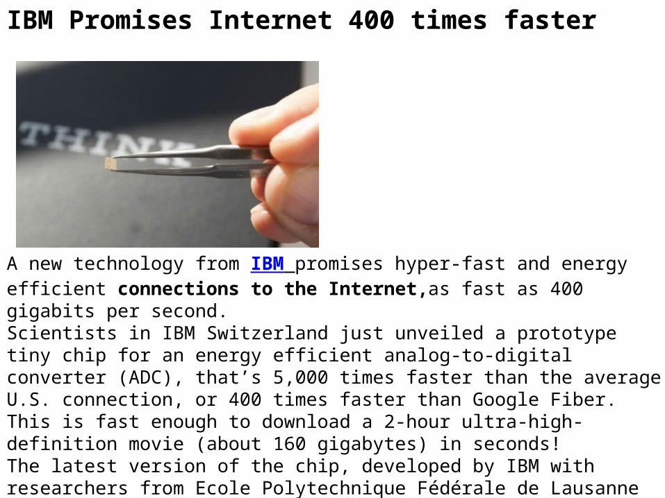
IBM Promises Internet 400 times faster
A new technology from IBM promises hyper-fast and energy efficient connections to the Internet,as fast as 400 gigabits per second. Scientists in IBM Switzerland just unveiled a prototype tiny chip for an energy efficient analog-to-digital converter (ADC), that’s 5,000 times faster than the average U.S. connection, or 400 times faster than Google Fiber.This is fast enough to download a 2-hour ultra-high-definition movie (about 160 gigabytes) in seconds!The latest version of the chip, developed by IBM with researchers from Ecole Polytechnique Fédérale de Lausanne in Switzerland, is only a prototype right now and was presented at the International Solid-State Circuits Conference (ISSCC) in San Francisco.
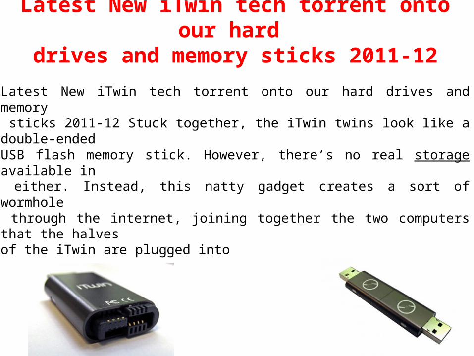
Latest New iTwin tech torrent onto our hard drives and memory sticks 2011-12
Latest New iTwin tech torrent onto our hard drives and memory sticks 2011-12 Stuck together, the iTwin twins look like a double-ended USB flash memory stick. However, there’s no real storage available in either. Instead, this natty gadget creates a sort of wormhole through the internet, joining together the two computers that the halves of the iTwin are plugged into

SD-GU064G2 SD-GU032G2 SD- GU016G2
Capacity 32GB 64GB 16GB
Maximum read speed 95MB/ sec
Maximum write speed 60MB/ sec
Shipped in April 2014, with prices ranging from $120 to $300.
TOSHIBA SD Memory

Toshiba develops, manufactures 19nm generation NAND Flash Memory with
world's largest density and smallest die size128 Gb capacity in a 3-bit-per-cell chip on a 170mm2 die23 Feb, 2012
TOKYO—Toshiba Corporation (TOKYO: 6502) today announced breakthroughs in NAND flash that secure major advances in chip density and performance. In the 19 nanometer (nm) generation, Toshiba has developed a 3-bit-per-cell 128 gigabit (Gb) chip with the world's smallest[1] die size—170mm2—and fastest write speed[2]—18MB/s of any 3-bit-per-cell device. The chip entered mass production earlier this month .

What's the largest memory stick that you can buy?
It is 256GB. It is a Memory Stick/Flash Drive/USB/Small Little Finger. It is
Very Expensive.128GB$1,499.99Item# SDCFXP-128G-A91SanDisk Extreme® Pro™ CompactFlash®
128GB Card with VPG
.
.
Jun 19, 2012 SANDISK I
Kingston 1TB USB3.0 DataTraveler HyperX
$899 Valid from Aug 05, 2014
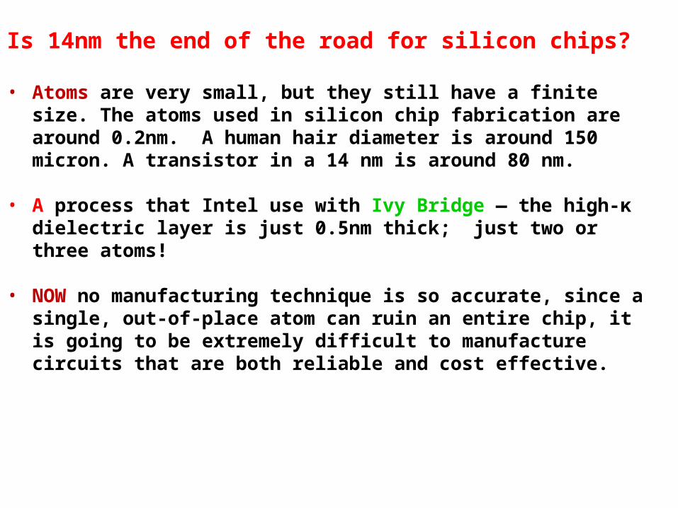
Is 14nm the end of the road for silicon chips?
• Atoms are very small, but they still have a finite size. The atoms used in silicon chip fabrication are around 0.2nm. A human hair diameter is around 150 micron. A transistor in a 14 nm is around 80 nm.
• A process that Intel use with Ivy Bridge — the high-κ dielectric layer is just 0.5nm thick; just two or three atoms!
• NOW no manufacturing technique is so accurate, since a single, out-of-place atom can ruin an entire chip, it is going to be extremely difficult to manufacture circuits that are both reliable and cost effective.

Chipmakers are working hard to reach the 5nm node, but, the industry has several challenges to overcome. Presently, the leading transistor candidates for 5nm are the usual suspects— III-V finFETs; gate-all-around; and nanowires. But the tunnel field-effect transistor (TFET) is also considered for its low power and low voltage, about 0.5 –volt
Putting TFETs and finFETs into production is difficult and may need III--‐V materials, nanowires and other complex technologies.
System Design Engineering community,Wed, April 30 2014,What foundary support is needed for any chip maker looking to develop 14/16 nm finFET ? a discussion with Steve Carlson, Director, office of Chief Strategy Officer, Cadence Design.http://chipdesignmag.com/sld/blog/2014/04/30/deeper-dive-wed-april-30-2014/
What is in store for us

CHALLENGES MOUNT FOR INTERCONNECT> By Mark LaPedus There are a plethora of chip-manufacturing challenges for the 20nm node and beyond. When asked what are the top challenges facing leading-edge chip makers today, Gary Patton, vice president of the Semiconductor Research and Development Center at IBM, said it boils down to two major hurdles: lithography and the interconnect.
ROUTING CONGESTION RETURNSBy Ed Sperling Routing congestion has returned with a vengeance to SoC design, feuled by the advent of more third-party IP, more memory, a variety of new features, as well as the inability to scale wires at the same rate as transistors.

Example of Industrial foundry
GLOBALFOUNDRIES provides advanced semiconductor manufacturing excellence with leading-edge (28nm), mainstream (65nm and 45nm) and mature (0.35um to 0.11um) technology, on both 200mm and 300mm wafers. GLOBALFOUNDRIES has fabrication in Dresden, New York and Singapore, with a network of design and support centers in Silicon Valley, China, Japan, Germany, Singapore, Taiwan and the U.K. WWW.GLOBALFOUNDRIES.COM
LEVERAGING THE PASTBy Ann Steffora Mutschler “It is easy to forget that not every design today is targeted at 20nm, given the amount of focus put on the bleeding edge of technology. But in fact a large number of designs utilize the stability and reliability of older manufacturing nodes, as well as lower mask costs, by incorporating new design and verification techniques,
3D design opens up architectural possibilities for engineering teams to realize much better performance and far less power consumption.
The greatest power savings in 3D designs are achieved at the architectural level, and that may mean jumping in at the deep end.
Hot topic: Thermal integrity's effect on 3D-IC design and analysis.
3D design

What Comes After FinFETs?By Mark LaPedus
The semiconductor industry is currently making a major transition from conventional planar transistors to finFETs starting at 22nm.The question is what’s next? In the lab, IBM, Intel and others have demonstrated the ability to scale finFETs down to 5nm or so. If or when finFETs runs out of steam, there are no less than 18 different next generation candidates that could one day replace today’s CMOS-based finFET transistors.Mayberry said the eventual winners and losers in the next-generation transistor race will be determined by cost, manufacturability and functionality. “The best device is the one you can manufacture,” he said.In fact, the IC industry is already weeding out the candidates. In 2005, the Semiconductor Research Corp. (SRC), a chip R&D consortium, launched the Nanoelectronics Research Initiative (NRI), a group that is researching futuristic devices capable of replacing the CMOS transistor in the 2020 timeframe. NRI member companies include GlobalFoundries, IBM, Intel, Micron and TI.http://extensionmedia.c.topica.com/maapRorab9Upkcc03nbcaeht4A/

posted on April 28, 2013 byStaff Writer
Top FPGA Companies For 2013
http://sourcetech411.com/2013/04/top-fpga-companies-for-2013/fpga_market_262x193/
These two companies comprise approximately 90% market share (Xilinx 47%, Altera 41%) in 2012 with combined revenues in excess of $4.5B and a market cap over $20B.
New materials and processes for advanced interconnectsAlthough on chip interconnects have not been scaling at the same speed as other parts of the chip, new capabilities enabled by graphene and CNTs, among other materials, could soon change that.http://marketing.electroiq.com/ct.html?ufl=b&rtr=on&s=x9w5u6,a0tz,5ke,km42,2wdj,fvk2,ca13
3D memory for future nanoelectronic systems3D memory will generally cost more than 2D memory, so generally a system must demand high speed or small size to mandate 3D. Communications devices and cloud servers need high speed memory. Mobile and portable personalized health monitors need low power memory. In most cases, the optimum solution does not necessarily need more bits, but perhaps faster bits or more reliable bits.http://marketing.electroiq.com/ct.html?ufl=b&rtr=on&s=x9w5u6,a0tz,5ke,8tkl,1r3y,fvk2,ca13
When it comes to memory manufacturing, consolidation is king.Today only three major DRAM manufacturers remain MICRON, SAMSUNG, and SK HYNIXSpectrum Jan 2014
How about interconnect and Memory

Compound Semiconductors Join the race to sustain Moore’s Law
Engineers at Imec and IBM have independently developed processes for making the next decade’s leading chips. The process involves using wafers and certain exotic materials compound semiconductors with ingredients from columns III and V of the old periodic table . The mixing materials holds the key to maintaining the traditional performance improvements associated with Moore’s Law and the shrinking of Transistors.Spectrum IEEE Jan 2014

All optical transistors“The Max Planck Institute of Quantum Optics has taken a step towards devising the long-awaited optical transistor. The technology could pave the way towards long-haul data transmissions using an all-optical network.Researchers from Max Planck have devised a type of optical transistor using a cloud of ultra-cold rubidium atoms.”.
http://semiengineering.com/manufacturing-bits-august-5/
Worldwide Semiconductor Revenue Grew 5 Percent in 2013, According to Final Results by Gartner• Intel Retained the No. 1 Position for the 22nd Year in a
Row Total worldwide semiconductor revenue reached $315 billion in 2013, up 5 percent from 2012, according to Gartner, Inc.
February Semiconductor Sales Up 11.4 Percent Compared to Last Year.
More Than One Fourth of Industry Wafer Capacity Dedicated to <40nm Process Geometries.
• • Semiconductor Market Forecast to Contract by 0.1 Percent in 2012 - First Decline in ThreeYears
State of Semiconductor Revenue

https://www.youtube.com/watch?v=eh3dA8xnZ4Y
Graphene The wonder Material

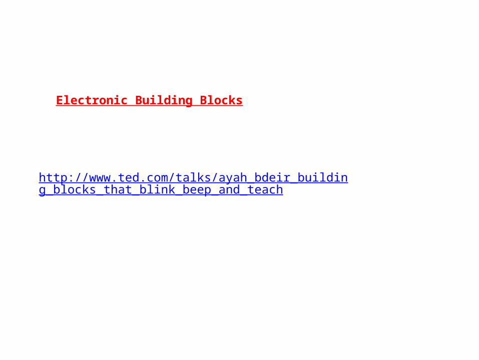
http://www.ted.com/talks/ayah_bdeir_building_blocks_that_blink_beep_and_teach
TED on Little Bits
http://www.ted.com/talks/ayah_bdeir_building_blocks_that_blink_beep_and_teach
Electronic Building Blocks

https://ca.finance.yahoo.com/news/microchips-implanted-healthy-people-sooner-152916800.html
Personal Chip Implant

We have seen nothing YET the best days are still aheadBrain ImprovementFor millions, the brain has not changed, but how we use it is changed. BUT NOW :• Genetically it is possible to alter the brain to create a super brain .• The future comes with new innovation (brain power) • We can upgrade our brain (With implants)• Increase memory (with implants)• Increase sensors (with implants)• Communication between Brain-Brain directly rather than converting chemical –
electrical-sounds-pressure waves-mechanical (mouth)-pressure movements (ear) –electrical- chemical, we should be doing it directly
• The most important development in the world has been technology starting with steam engine, ie replacing human muscle with machine, which is more powerful… So what happens if we increase our brain power, then what we can do !!
https://www.youtube.com/watch?v=Z8HeFNJjuj0 Smarter DevicesDigital Technology as it gets smarter is eating up our jobs ( example : copier.. translators, Articles written by machines, driverless cars, trucks.. )Economies do not run on energy, labor , or capital The future is with innovation

CONCORDIAVLSI DESIGN LAB
42
AIMs What the customers want: High Quality Low Cost Small Size/Weight
What the Employer wants Design the: Best Cheapest In shortest time Follow the Spec or better.
What you (chip designer) should do: Design a chip with: High speed Small area Low power Testable and reliable Delivered in a short time

CONCORDIAVLSI DESIGN LAB
43
Instructor Name: Asim Al-KhaliliOffice: EV5.126
Tel: 514 848-2424 ext.3119, FAX 848 2802Email [email protected]
Web http://www.ece.concordia.ca/~asimTime: Mondays-Wednesdays 16:15-17:30
Class Room: To be announced (MB- 1-301)Office hours: Wednesdays 2:00- 3:30
Course OutlineReference Materials
AssignmentsLectures Information
AnnouncementsTools
ProjectUseful Files
Important Dates:
Midterm Exam: ,Wednesday 14th Oct,2014 Final Exam: Exam: To be announced
Project Delivery: Monday 7th Dec. 2015, at 2:00 pm. To be handed to me in my office or the Secretary at front desk.
Web Information

CONCORDIAVLSI DESIGN LAB
44
The following topics will be covered:Week_1 Introduction to ASIC design and review materials. Week_2 MOS transistor characteristics. Week_3 DC analysis of CMOS logic family. Week_4 RC time models, interconnect models. Week_5 Transient analysis, propagation delay models. Week_6 CMOS gates and Static logic families. Week_7 Memory elements. Clocking strategies. Week_8 CMOS process and layout generation.Week_9 Layout techniques. Week_10 I/O drivers and circuit protection.Week_11 Circuit Optimization and secondary effects. Week_12 Dynamic logic families. Week_13 Design for Testability, Packaging, PLD, Synthesis issues. Laboratory: H915. The lab is conducted as an open concept, with no schedule. Information on lab usage will be provided in class.Grading: 5% Assignment Midterm 15% 20% project, 60% Final ExamText: “CMOS Digital Integrated Circuits, Analysis and Design” (Recommended ) By Sung-Mo Kang and Yusuf Leblebici,3rd Edition, Published by McGraw-Hill “Principles of CMOS VLSI Design” By N. H. Weste & K. Eshraghian 2nd Edition, Published by Addison Wesley “ Application Specific Integrated Circuits”, By M. J. S. Smith,,Addison Wesley

CONCORDIAVLSI DESIGN LAB
45
Device PhysicsDevice
Electronics
Transistor Circuits
Combinational and sequential Logic Circuits
Regular and irregular Subsystems
System related issues including reliability, DFT
Covered in COEN 451
CONCORDIAVLSI DESIGN LAB
46
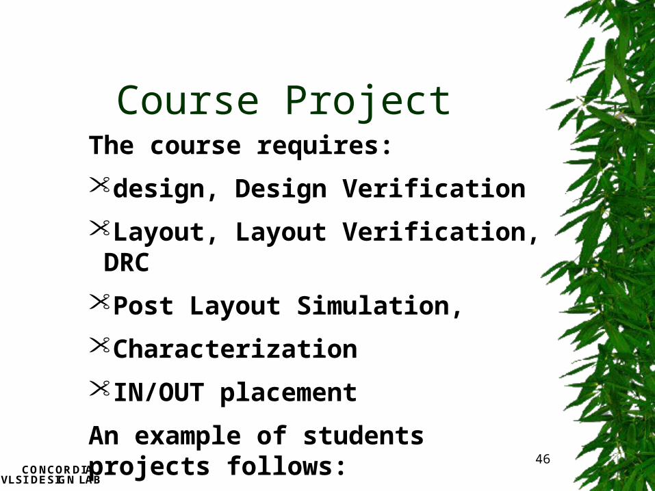
Course ProjectThe course requires:
• design, Design Verification
• Layout, Layout Verification, DRC
• Post Layout Simulation,
• Characterization
• IN/OUT placement
An example of students projects follows:

Scientific Process or method: Sir Francis Bacon Formulation of a question: Why the apple falls down and not up? Hypothesis: based on knowledge obtained while formulating the
question Prediction: This step involves determining the logical consequences
of the hypothesis Testing /experimentation: This is an investigation of whether the real
world behaves as predicted by the hypothesis. Analysis: This involves determining what the results of the
experiment show and deciding on the next actions to take Theory

LearningIf you're going to learn anything, you need two kinds of prior knowledge:
knowledge about the subject at hand, like math, sciences, or programming
knowledge about how learning actually works, ie understanding of the cognitive strategies that allow people to learn well.
Suggestions to help you learn: Force yourself to recall.
In your mind repeat what you have read and see if you can recall what you have just read. Flashcards are useful in this, since they force you to supply answers.
Connect the new thing to the old things in your brain.
When you do that you are creating new web-lines, in your web of knowledge(Connections between Neurons) that will stick in your brain.
Reflect.
At the end of your learning session reflect in your mind what you have learned.Henry Roediger and Mark McDaniel, psychologists at Washington University in St. Louis and coauthors of " Make It Stick: The Science Of Successful Learning”

Life• When passing a flower, stop and smell it and look at it and
appreciate it. Life moves on, so stop and look at the good things around you.
• Be Happy with what you can do and ignore the things that you did not succeed to do.
• Have a good social life and surround yourself with people that have the same wave length and hobbies so that you can be yourself amongst them .
• Keep your hopes alive and keep moving forward by looking forward to what you want to achieve. Keep doing new things and learn new things.
• Enjoy the present, consider every breath is a present

Tools
Cadence unveiled two new tools. The first is a rapid prototyping platform that the company claims will shorten bring-up time by 70%, with 4X improvements in capacity, with IEEE 1801 support for low-power verification through its emulation platform. The second is a single and multi-corner custom/analog extraction tool, which it claims will improve performance by 5X. The tool has been certified for TSMC’s finFET process.

CONCORDIAVLSI DESIGN LAB
511980
0.1nm
1nm
10 nm
0.1m
1m
10m
100m
Feature Size
Year
Transition Region
Atomic Dimensions
Quantum Devices
0.18 in 1999
Integrated CircuitHistory
ITR Roadmap
2000 2020 20401960
The Future for Feature Size

CONCORDIAVLSI DESIGN LAB
52
2001
2000
1999
0 100 200 300 400 500 600 700 0
10
20
30
40
50
Junction Depth (nm)
Sheet Resistance (/sq)
800
60
2002
2003
2004 2005
2008
2011
2014
The Future of Junction Depth

CONCORDIAVLSI DESIGN LAB
53
Power density Evolution
Feature size (µm)
Watts/cm2

CONCORDIAVLSI DESIGN LAB
54
Power Consumption

CONCORDIAVLSI DESIGN LAB
55
GateOverDrive
Supply Voltage
Vth
1980 1985 1990 1995 2000 2005 2010 20150
1
2
3
4
5
Year
Volts The Future for Supply Voltage

CONCORDIAVLSI DESIGN LAB
56
Optical Communications

A day made of Glasshttp://www.youtube.com/watch?v=X-GXO_urMow&playnext=1&list=PL00407EB774FA759B&feature=results_main
CONCORDIAVLSI DESIGN LAB
58
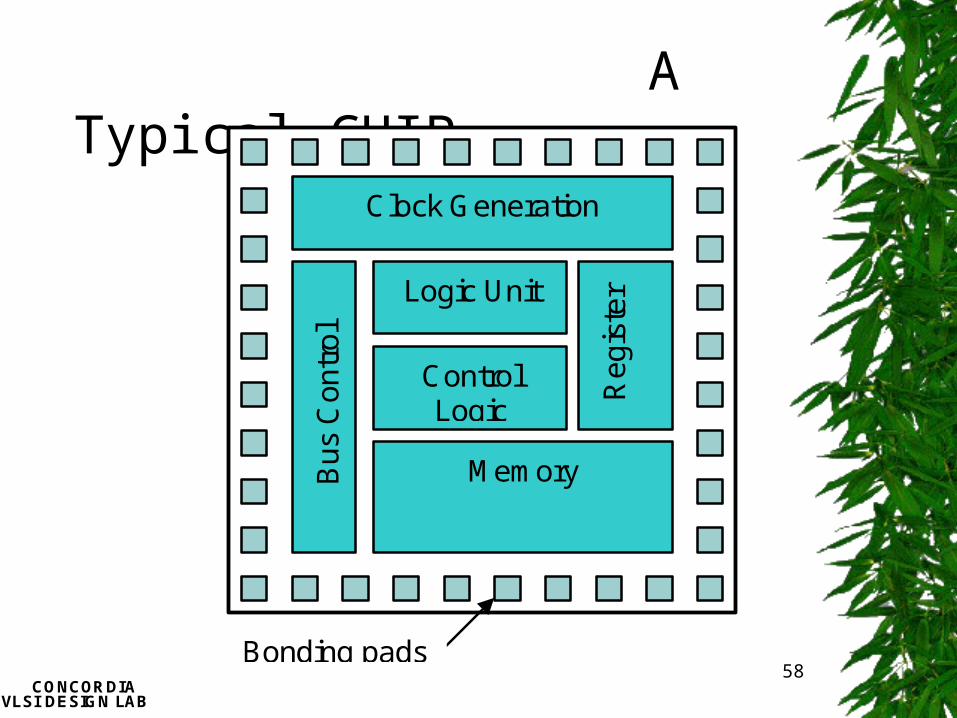
Logic Unit
Bus
Con
trol
Memory
Clock Generation
Reg
iste
rLogic Unit
ControlLogic
Bonding pads
A Typical CHIP

CONCORDIAVLSI DESIGN LAB
59
Design Abstraction Levels
Prentice Hall/Rabaey
n+n+S
G D
+
DEVICE
CIRCUIT
GATE
MODULE
SYSTEM

CONCORDIAVLSI DESIGN LAB
60
CMOS System Design Top-down Design:
Design starts at System Specification and works its way to bottom, ie. circuit level
Bottom-up design: Design starts at the basic circuits and works
upwards towards system level structure
CONCORDIAVLSI DESIGN LAB
61
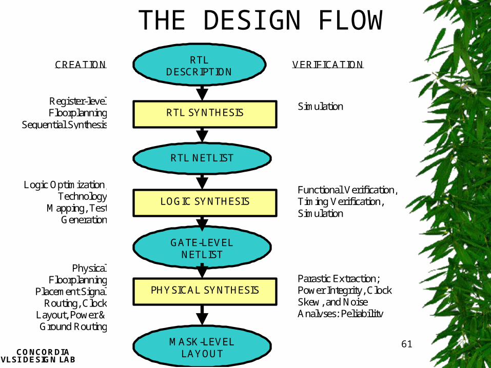
RTL SYNTHESIS
RTL NETLIST
LOGIC SYNTHESIS
GATE-LEVEL NETLIST
PHYSICAL SYNTHESIS
MASK-LEVEL LAYOUT
RTL DESCRIPTION
CREATION
Register-level Floorplanning
Sequential Synthesis
Logic Optimization, Technology
Mapping, Test Generation
Physical Floorplanning
Placement Signal Routing, Clock
Layout, Power & Ground Routing
VERIFICATION
Simulation
Functional Verification, Timing Verification, Simulation
Parastic Extraction; Power Integrity, Clock Skew, and Noise Analyses; Peliability Analysis
THE DESIGN FLOW
CONCORDIAVLSI DESIGN LAB
62
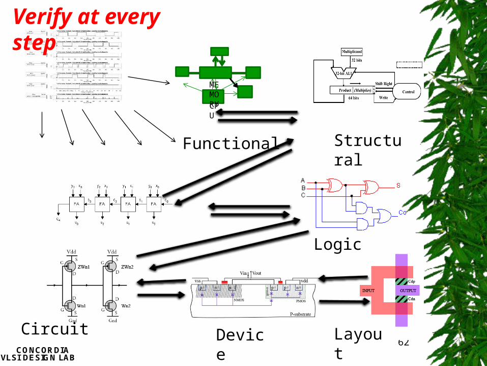
Verify at every step
LayoutDeviceCircuit
Logic
Structural
CPU
MEMORY
Functional

CONCORDIAVLSI DESIGN LAB
Design Strategies
Hierarchy– A repeated process of dividing large
modules into smaller sub-modules until the complexity of sub-modules are at an appropriately comprehensible level of detail.
– Parallel hierarchy is implemented in all domains.

CONCORDIAVLSI DESIGN LAB
Regularity Divide the hierarchy in to similar building blocks
whenever possible. Some programmability could be added to achieve
regularity.
Modularity Well defined behavioural, structural and physical
interface. Helps: divide tasks into well defined modules,
design integration, aids in team design.
Locality Internals of the modules are unimportant to any
exterior interface.
A Structured Design
CONCORDIAVLSI DESIGN LAB
IC Design Methodology Requirement specification
– most important function which impacts the ultimate success of an IC relates to how firm and clear the device specifications are.
– Device specification may be updated throughout the design cycle.
– Main items in the specifications are: functional intent: brief description of the device,
the technology and the task it performs. Packaging specification
– device port number– package type, dimension, material
CONCORDIAVLSI DESIGN LAB
high-level block diagram: all major blocks including intra block connections and connections to pin-outs indicating direction and signal flow.
Intra block signal function: description of how blocks interact with each other supported with timing diagram where necessary.
· Internal block description of internal operation of each block. Where necessary, the following to be included: timing diagram, state diagram, truth table.
Functional Description

CONCORDIAVLSI DESIGN LAB
I/O specifications· pin-out diagram· I/O functional description· loading· ESD requirements· latch-up protection
D.C. specifications· absolute maximum ratings for: supply voltage,
pin voltages· main parameters: VIL and VIH for each input,
VOL and VOH for each output, input loading, output drive, leakage current for tri-state operation, quiescent current, power-down current (if applicable)
Specifications

CONCORDIAVLSI DESIGN LAB
AC specifications· inputs: set-up and hold times, rise and fall times
· outputs: propagation delays, rise and fall times, relative timing
· critical thinking
Environmental requirements· operating temperature, storage temperature,
humidity condition (if applicable)
Testing
Specification, continued
CONCORDIAVLSI DESIGN LAB
Device Specification Functional intent: briefly describe the
device, the technology, and the circuits it will replace as well as the task it will perform.
Design concept pin-out diagram: describe the device using a
block diagram of the external view of the chip - basically, a box with all the I/O pins labelled and numbered
I/O description: use a chart to define the I/O signals shown in the pin-out diagram

CONCORDIAVLSI DESIGN LAB
Example:Pin # Pin Name I/O Type Function
P1 VDD PowerSupply
PowerSupply, +5Vdc withrespect toVSS
P2 TXCLK Input TransmitClock, 5.12MHz rate
P3 TXP1 Output Transmitoutput –channel 1,+ve polarity

CONCORDIAVLSI DESIGN LAB
internal block diagram: draw blocks for major functions, show all connections including: connection to all pin-outs, connections between blocks, and direction of signal flow
Inter-block signal function: describe how the blocks interact with each other and support this with timing diagrams where necessary
· internal block description: describe the internal operation of each block. When necessary, include: timing diagrams, state diagrams, and truth table
Functional Specification

CONCORDIAVLSI DESIGN LAB
Operating characteristics Absolute maximum stress ratings.
Example:
Parameter Symbol Min. Max. Unit
Storage T Ts -65 +150 OCOperating T TA -40 +85 OC
Supply V VDD -0.5 7 V
Input V VI -0.3 VDD + 3 V
Supply I IDD 5 mA

CONCORDIAVLSI DESIGN LAB
Operating power and environmental requirement:
· power supply voltage
· operating supply current (specify conditions, e.g., power up, power down, frequency, output conditions)
· storage temperature
· operating temperature
· humidity conditions (if applicable)
Requirements
CONCORDIAVLSI DESIGN LAB
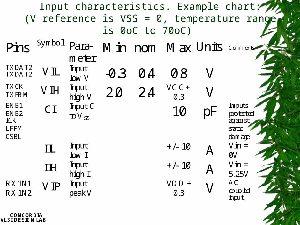
Input characteristics. Example chart:(V reference is VSS = 0, temperature range is 0oC
to 70oC)
Pins Symbol Para-meter
Min nom Max Units Comments
TXDAT2TXDAT2
VIL Inputlow V
-0.3 0.4 0.8 VTXCKTXFRM
VIH Inputhigh V
2.0 2.4 VCC +0.3
VENB1ENB2ICKLFPMCSBL
CI Input Cto VSS
10 pF Imputsprotectedagainststaticdamage
IIL Inputlow I
+/- 10 A Vin =0V
IIH Inputhigh I
+/- 10 A Vin =5.25V
RX1N1RX1N2
VIP Inputpeak V
VDD +0.3
V ACcoupledinput

CONCORDIAVLSI DESIGN LAB
Regularity Divide the hierarchy in to similar building blocks
whenever possible. Some programmability could be added to achieve
regularity.
Modularity Well defined behavioural, structural and physical
interface. Helps: divide tasks into well defined modules, design integration, aids in team design.
Locality Internals of the modules are unimportant to any
exterior interface.
A Structured Design
CONCORDIAVLSI DESIGN LAB
76
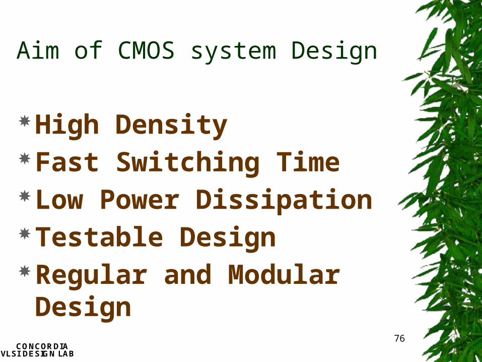
Aim of CMOS system Design
High DensityFast Switching TimeLow Power DissipationTestable DesignRegular and Modular Design

CONCORDIAVLSI DESIGN LAB
77
System Performance This is related to several factors
including: Algorithm design Design strategy Circuit implementation Floor plan Interconnect strategy Input/Output drives and coupling Clock distribution Interfacing

CONCORDIAVLSI DESIGN LAB
78
Standard Devices General purpose use --not optimized to a specific application
* Fixed or programmable
* Available in various complexities:
SSI, MSI, LSI, VLSI, and ULSI
* Function: standard logic, MPU, memories, DSP, analog functions
* Available in a variety of packages
* Technology: bipolar, nMOS, CMOS, BiCMOS, GaAs
* Occupy larger areas and consume more power compared to other types of ICs
CONCORDIAVLSI DESIGN LAB
79
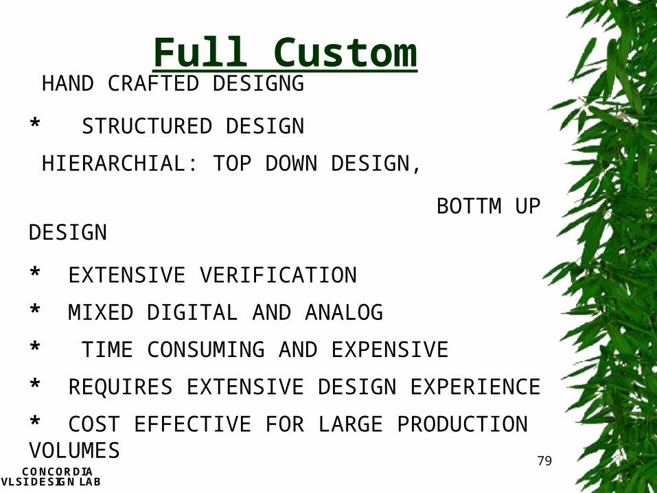
Full Custom HAND CRAFTED DESIGNG
* STRUCTURED DESIGN
HIERARCHIAL: TOP DOWN DESIGN,
BOTTM UP DESIGN
* EXTENSIVE VERIFICATION
* MIXED DIGITAL AND ANALOG
* TIME CONSUMING AND EXPENSIVE
* REQUIRES EXTENSIVE DESIGN EXPERIENCE
* COST EFFECTIVE FOR LARGE PRODUCTION VOLUMES
CONCORDIAVLSI DESIGN LAB
80
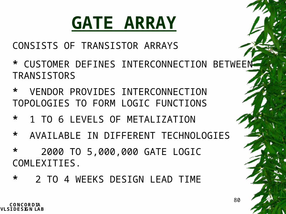
GATE ARRAYCONSISTS OF TRANSISTOR ARRAYS
* CUSTOMER DEFINES INTERCONNECTION BETWEEN TRANSISTORS
* VENDOR PROVIDES INTERCONNECTION TOPOLOGIES TO FORM LOGIC FUNCTIONS
* 1 TO 6 LEVELS OF METALIZATION
* AVAILABLE IN DIFFERENT TECHNOLOGIES
* 2000 TO 5,000,000 GATE LOGIC COMLEXITIES.
* 2 TO 4 WEEKS DESIGN LEAD TIME

CONCORDIAVLSI DESIGN LAB
81
STANDARD CELLS*PREDESIGNED AND PRECHARACTERIZED CELLS
* AVAILABLE IN VARIOUS CELL COMPLEXITIES:
MACROCELLS --VARIABLE HEIGHTS
MICROCELLS--STANDARD HEIGHTS
* DESIGN PHILOSOPHY SIMILAR TO OFF THE SHELF COMPONENTS
* MORE EFFICIENT SILICON UTILIZTION COMPARED
* MEDIUM DESIGN TIME
* LOWER COST
* COST EFFECTIVE FOR LARGE PRODUCTION VOLUMES*

CONCORDIAVLSI DESIGN LAB
82
CELL TOPOLOGYSTANDARD CELLS ARE AVAILABLE AS FIXED HEIGHT OR VARIABLE HEIGHT.
*FIXED HEIGHT CELLS:
--MAJORITY OF CELLS ARE IMPLEMENTED USING
-- FIXED HEIGHT, BUT VARIABLE WIDTH LAYOUT
-- CELLS ARE STACKED IN ROWS
* VARIABLE HEIGHT CELLS :
--FOR MORE COMPLEX FUNCTIONS SUCH AS MEMORY, ALU, MICROPROCESSOR
* COST EFFECTIVE FOR LARGE PRODUCTION VOLUMES

CONCORDIAVLSI DESIGN LAB
83
-- Project of ASIC Design --
Instructor: Dr. A.J.AL-Khalili
Submitted byJi, Haiying Zhang, Haiqing
Submitted Date: 29 April, 2002

CONCORDIAVLSI DESIGN LAB
84
OverviewLogic Design Specification: exhibiting our logic design of every unit: half adder/subtracter, one-bit counter, 4-bit counter. Logic circuit simulation result is presented. The stage mainly worked on the Synopsys development platform within UNIX.
Circuit Design Specification: fully covering the most of our work about every CMOS logic circuit unit: NAND and NOR gates, D flip-flop etc. All parameters of circuits are decided. And there are some the circuit plots and waveforms generated by Cadence development tools that test and verify every part of our CMOS circuit design.
Layout and Simulation: With Cadence layout tool, we drew the layouts of all circuit units according to the design parameter from the last design stage. Perform DRC. Extract the design and simulate it again and characterize the two gates. To perform DRC on the final design, extract it and simulate it again to obtain the performance measures. The waveforms related the design are shown and analyzed.
Packaging: The procedure to place and rout the complete chip including all I/O drivers and PADs is presented.
Analyzing and Summary: The test results were analyzed carefully and helped us got appropriate conclusion. Give a complete specification for the circuit. It is summary of our work. It manifests our great gain of designing and developing work experience and important realization from this course.
Appendix: this is needful supplement showing our coding work in logic design stage and perfect layout picture drawn with Cadence layout tools.

CONCORDIAVLSI DESIGN LAB
85
L o g i c D e s i g n
P o r t F u n c t i o nc l k D F F D r i v i n g C l o c k , 1 - 0 : i n p u t -
o u t p u tc l r “ 1 ” c l e a r a l l p o r tu d c t r l 1 : u p c o u n t i n g
0 : d o w n c o u n t i n gi n p u t 1 o r 0s o u t 0 0 0 0 - - 1 1 1 1b r w c r y B o r r o w o r c a r r y s i g n a l ; f o r u p
l i n k i n g
4 – B i tU p / D o w n
C o u n t e rCLK

CONCORDIAVLSI DESIGN LAB
86
Up/ Down controlling-Half adder and subtracter design
Half-Adder and Half-Substracter function:Sout =A’B+B’ACarry=ABBorrow=BA’
The Up/Down Control signal is added to the unit. It just controls which one should be output either the carry orborrow.
Borcar=B(UD’A’+UD*A) (UD: up/down control)When UD=1, output carry, the unit works as a half adder. When UD=0, output borrow, it works as a halfsubstracter.
CONCORDIAVLSI DESIGN LAB
87
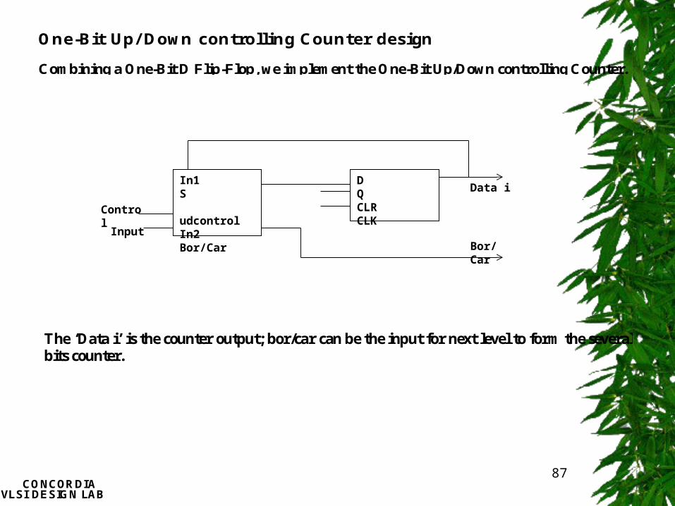
One-Bit Up/ Down controlling Counter design
Combining a One-Bit D Flip-Flop, we implement the One-Bit Up/Down controlling Counter.
In1 S
udcontrolIn2 Bor/Car
D QCLRCLK
Input
Control
Data i
Bor/Car
The ‘Data i’ is the counter output; bor/car can be the input for next level to form the severalbits counter.

CONCORDIAVLSI DESIGN LAB
88
4-Bit Up/ Down controlling Counter Logic Circuit Plan and Simulation
Using four One-Bit Up/Down controlling Counters, we implement the 4-Bit Up/Down controllingCounter unit shown as following figure.

CONCORDIAVLSI DESIGN LAB
89
We tested and verified the design within Synopsys simulation platform on the Unix(Sun-Solaris). The waveform is shown as Figure 3-6.
Figure 3-6

CONCORDIAVLSI DESIGN LAB
90
Circuit Design
D flip-flop circuit design
CONCORDIAVLSI DESIGN LAB
91
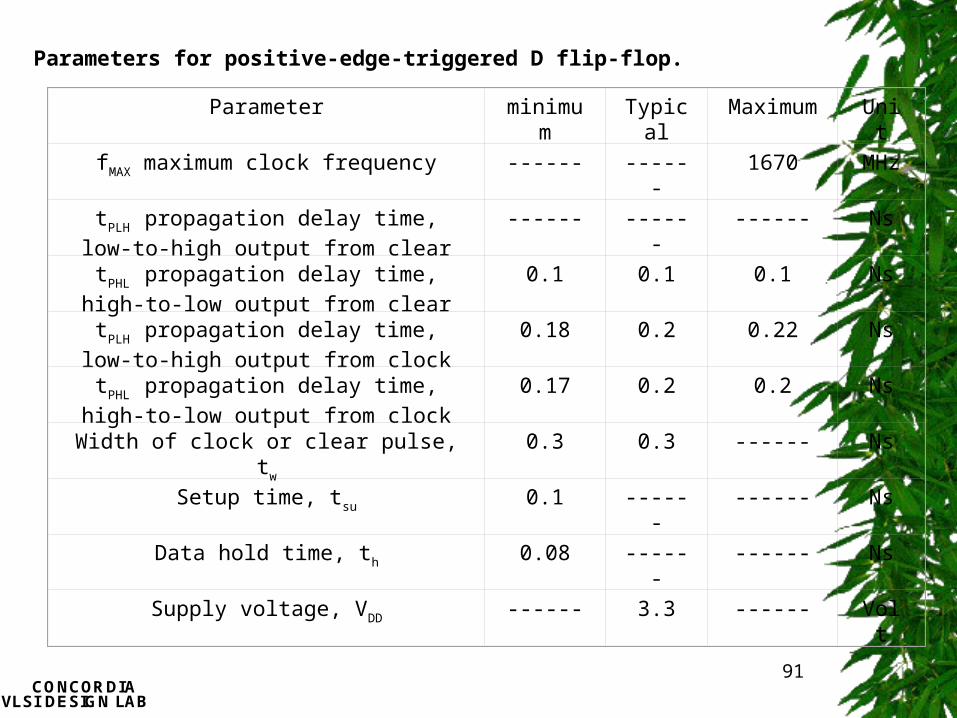
Parameter minimum Typical Maximum Unit
fMAX maximum clock frequency ------ ------ 1670 MHz
tPLH propagation delay time, low-to-high
output from clear
------ ------ ------ Ns
tPHL propagation delay time, high-to-low
output from clear
0.1 0.1 0.1 Ns
tPLH propagation delay time, low-to-high
output from clock
0.18 0.2 0.22 Ns
tPHL propagation delay time, high-to-low
output from clock
0.17 0.2 0.2 Ns
Width of clock or clear pulse, tw 0.3 0.3 ------ Ns
Setup time, tsu 0.1 ------ ------ Ns
Data hold time, th 0.08 ------ ------ Ns
Supply voltage, VDD ------ 3.3 ------ Volt
Parameters for positive-edge-triggered D flip-flop.

CONCORDIAVLSI DESIGN LAB
92
Timing waveforms of DFF

CONCORDIAVLSI DESIGN LAB
93
Half Adder/Subtracter Circuit

CONCORDIAVLSI DESIGN LAB
94
Half Adder/Subtracter Circuit waveforms
CONCORDIAVLSI DESIGN LAB
95
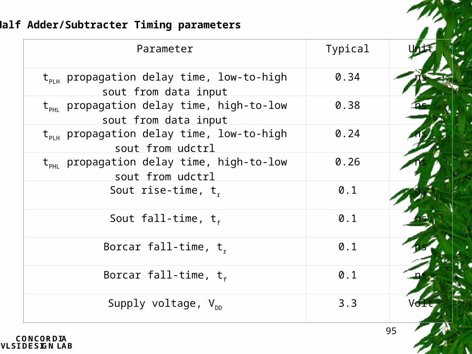
Half Adder/Subtracter Timing parameters
Parameter Typical Unit
tPLH propagation delay time, low-to-high sout from data input 0.34 ns
tPHL propagation delay time, high-to-low sout from data input 0.38 ns
tPLH propagation delay time, low-to-high sout from udctrl 0.24 ns
tPHL propagation delay time, high-to-low sout from udctrl 0.26 ns
Sout rise-time, tr 0.1 ns
Sout fall-time, tf 0.1 ns
Borcar fall-time, tr 0.1 ns
Borcar fall-time, tf 0.1 ns
Supply voltage, VDD 3.3 Volt

CONCORDIAVLSI DESIGN LAB
96
4-bit synchronous up/down counter design
4-bit synchronous up down counter implementation

CONCORDIAVLSI DESIGN LAB
97
waves feature for the 4-bit synchronous up down counter

CONCORDIAVLSI DESIGN LAB
98
Timing parameters for the 4-bit synchronous up down counter
Parameter Typical Unit
tPLH propagation delay time, low-to-high sout from clock input 0.34 ns
tPHL propagation delay time, high-to-low sout from clock input 0.43 ns
tPLH propagation delay time, low-to-high sout from udctrl 0.68 ns
tPHL propagation delay time, high-to-low sout from udctrl 0.60 ns
Sout rise-time, tr 0.38 ns
Sout fall-time, tf 0.36 ns
Borcar fall-time, tr 0.1 ns
Borcar fall-time, tf 0.1 ns
Supply voltage, VDD 3.3 Volt
CONCORDIAVLSI DESIGN LAB
99
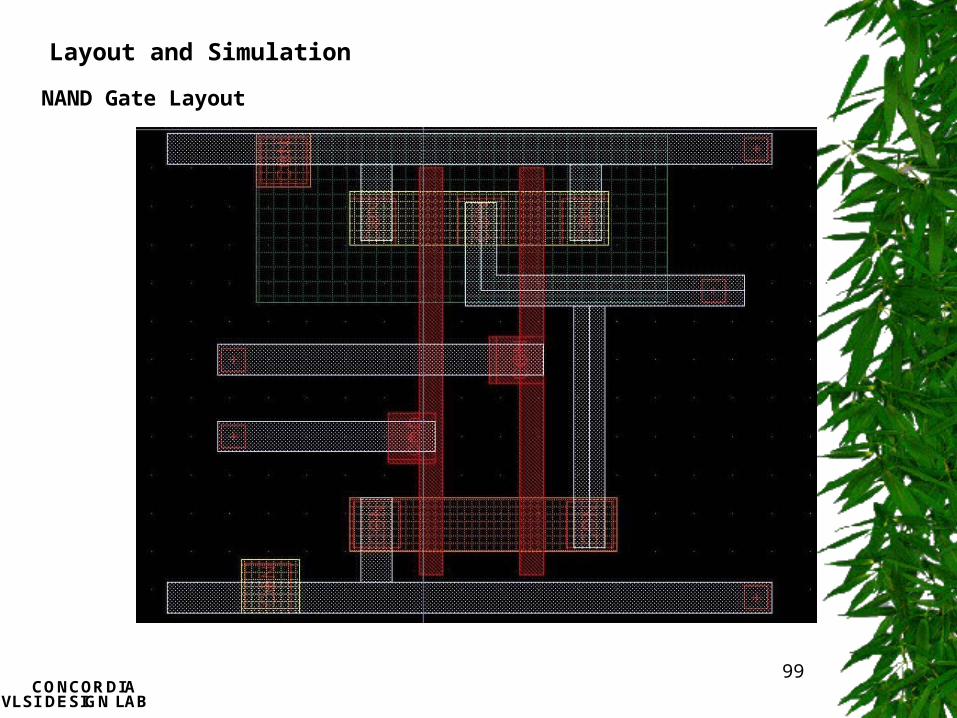
Layout and Simulation
NAND Gate Layout

CONCORDIAVLSI DESIGN LAB
100
simulation waveforms of NAND gate

CONCORDIAVLSI DESIGN LAB
101
Simulation characteristics of the 2-input NAND gate in complementary CMOS.
DC characteristicsActive area
Total area
Static current
VOH VOL VIH VIL NML NMH
18.76 um2
132.5 um2
0 3.3 volts
0 volt 1.42 volts
0.87 volts
0.87 volts
1.88 volts
AC characteristicstPLH
min
tPHL
min
tP
min
tPLH
max
tPHL
max
tP
max
tr
min
tf
min
tr
max
tf
max
Average power
PeakPower
0.15 ns
0.03ns
0.09 ns
0.18 ns
0.05 ns
0.115 ns
0.15 ns
0.14 ns
0.176 ns
0.15 ns
0.43 mw 0.5 mw
CONCORDIAVLSI DESIGN LAB
102
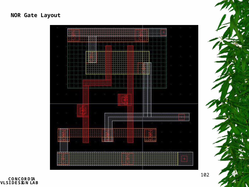
NOR Gate Layout

CONCORDIAVLSI DESIGN LAB
103
Waveform of the 2-input NOR gate in complementary CMOS.
CONCORDIAVLSI DESIGN LAB
104
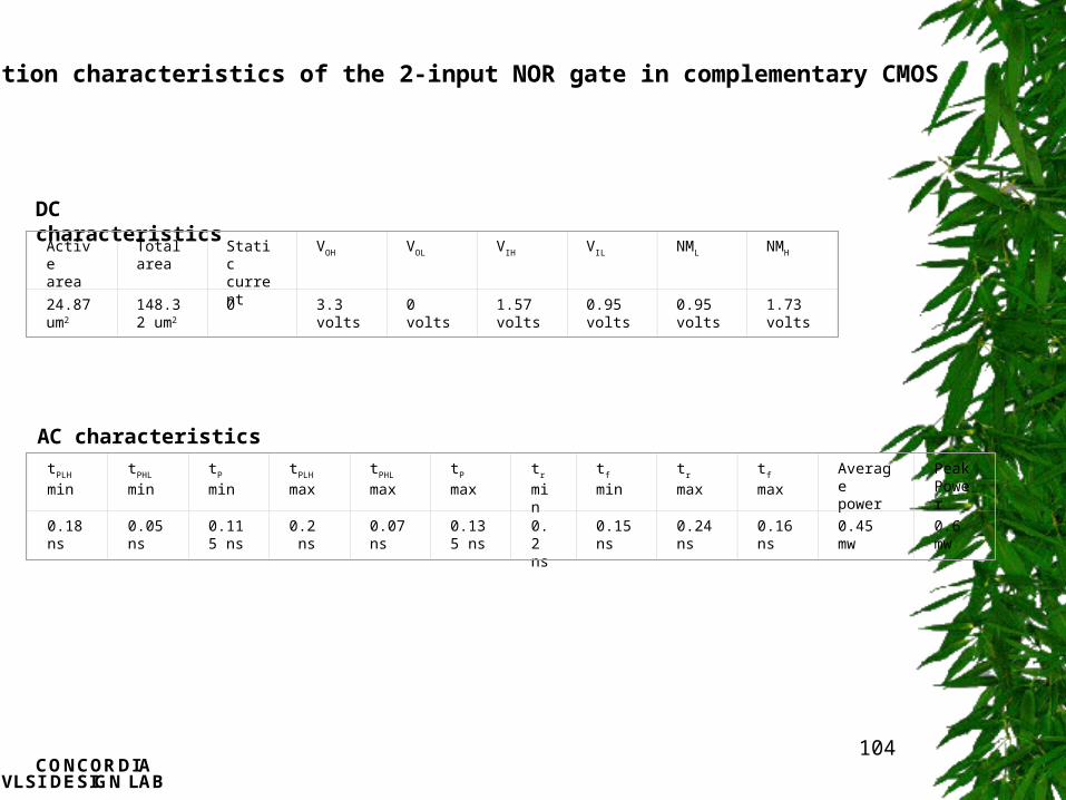
DC characteristics
Active area
Total area
Static current
VOH VOL VIH VIL NML NMH
24.87 um2
148.32 um2
0 3.3 volts 0 volts 1.57 volts
0.95 volts
0.95 volts
1.73 volts
AC characteristics
tPLH
min
tPHL
min
tP
min
tPLH
max
tPHL
max
tP
max
tr
min
tf
min
tr
max
tf
max
Average power
PeakPower
0.18 ns
0.05 ns
0.115 ns
0.2 ns
0.07 ns
0.135 ns
0.2 ns
0.15 ns
0.24 ns
0.16 ns
0.45 mw 0.6 mw
Simulation characteristics of the 2-input NOR gate in complementary CMOS
CONCORDIAVLSI DESIGN LAB
105
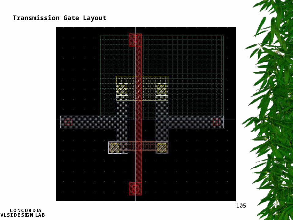
Transmission Gate Layout
CONCORDIAVLSI DESIGN LAB
106
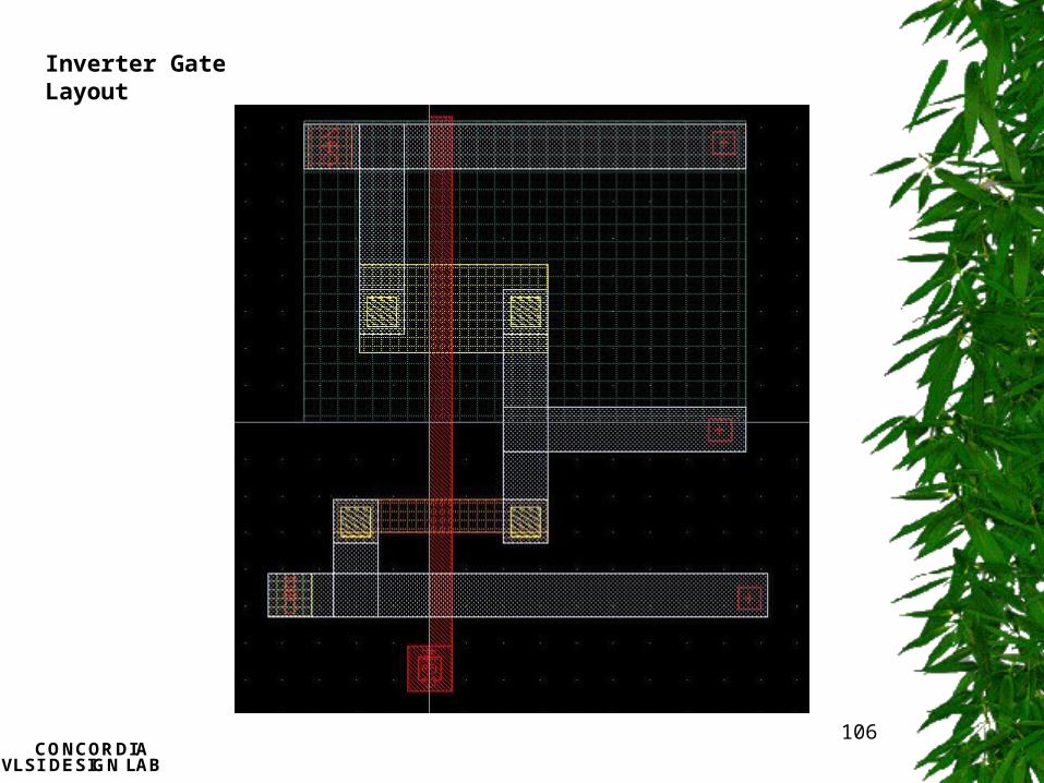
Inverter Gate Layout
CONCORDIAVLSI DESIGN LAB
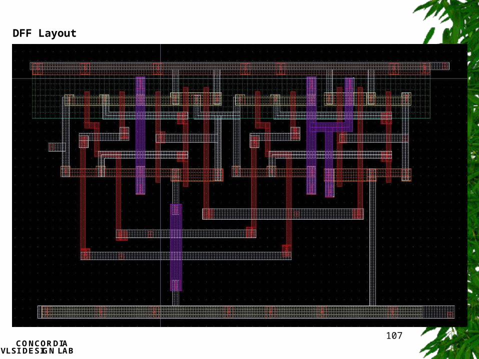
107
DFF Layout

CONCORDIAVLSI DESIGN LAB
108
Half Adder/Substrater Layout

CONCORDIAVLSI DESIGN LAB
109
4-bit synchronous up/down counter layout
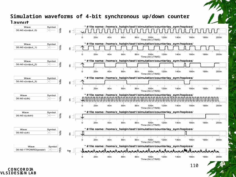
CONCORDIAVLSI DESIGN LAB
110
Simulation waveforms of 4-bit synchronous up/down counter layout

CONCORDIAVLSI DESIGN LAB
111
Simulation characteristics of 4-bit synchronous up/down counter layout
DC characteristics
Active area
Total area
Static current
VOH VOL VIH VIL NML NMH Input leakage current
2685um2
16000 um2
0 3.3 volts 0 volt
1.5 volts 0.9 volts 0.9 volts 1.8 volts 2 uA
Prerequisite for switching function
Maximum frequency fma
MinimumCLK width
MinimumCLR width
Set up time tsu uctrl to
CLK
Set up time tsu
CLR to CLK
Hold time th
uctrl to CLK
Hold time th CLR to
CLK
280 MHz 3.5ns
1.6ns
0.8 ns
0.3ns
0ns
0.15ns
Switching characteristics
tPLH tPHL tPudctrl to output tPLH tPHL tPCLK to output tPLH tPHL tP CLR to output
0.7 ns 0.7 ns 0.7 ns 0.665ns 0.72 ns 0.693 ns -------- 0.8 ns 0.8 ns
CONCORDIAVLSI DESIGN LAB
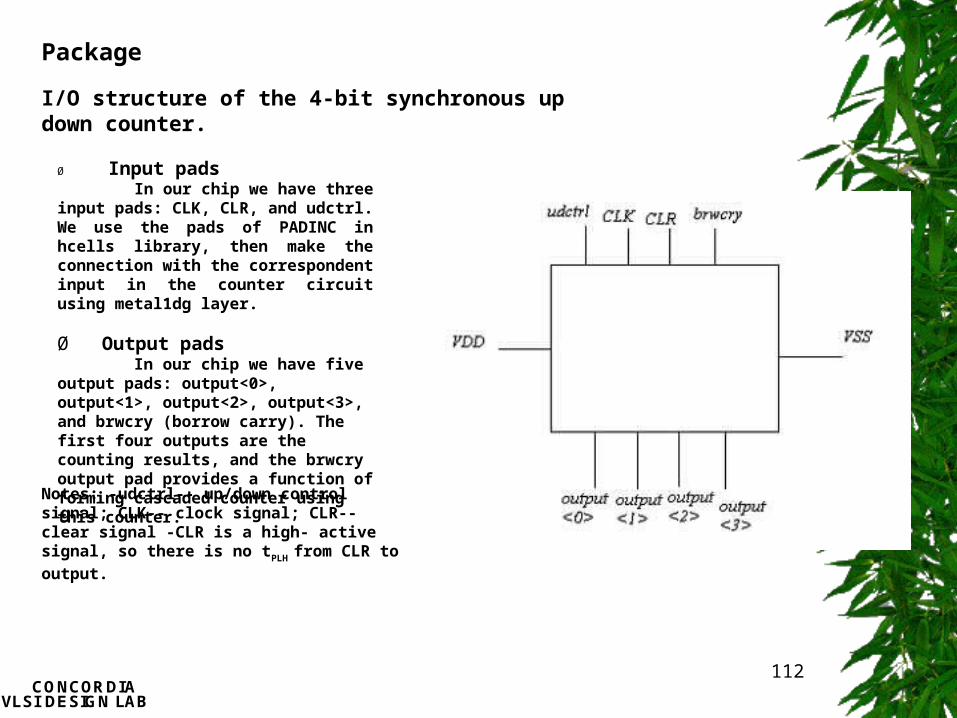
112
Package
I/O structure of the 4-bit synchronous up down counter.
Ø Input pads In our chip we have three input pads: CLK, CLR, and udctrl. We use the pads of PADINC in hcells library, then make the connection with the correspondent input in the counter circuit using metal1dg layer. Ø Output pads In our chip we have five output pads: output<0>, output<1>, output<2>, output<3>, and brwcry (borrow carry). The first four outputs are the counting results, and the brwcry output pad provides a function of forming cascaded counter using this counter.
Notes: -udctrl-- up/down control signal; CLK-- clock signal; CLR-- clear signal -CLR is a high- active signal, so there is no tPLH from CLR to output.
CONCORDIAVLSI DESIGN LAB
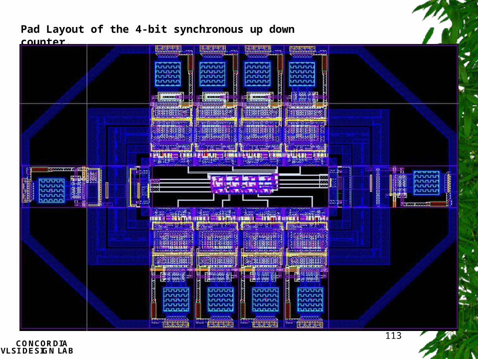
113
Pad Layout of the 4-bit synchronous up down counter.

CONCORDIAVLSI DESIGN LAB
114
Analyzing & Summary
From the three development stages, logic design, circuit design and layout simulation, we are able to acquire the conclusion easily. The logic design simulation is the ideal wave that we want to get. The circuit design simulation verifies our logic design correct and in this stage it also help us decide the appropriate parameters. The layout is based on our circuit design parameter. Its simulation result proves to our design work successful. What should be advanced is the fact that there is some discrepancy between the two results from circuit design simulation and layout simulation. As the shown in the Figure 5-5 and Figure 4-10, all the time performance parameters from layout simulation are higher those from circuit design simulation. Actually it is just right result that we have predicted. The layout is closer to real product. However, the circuit design mainly simulates the ideal model; some effect resulting from whole circuit can not be calculated accurately. In short, our work is proved to be significant. Through the project we have learned more system development knowledge and strengthened the ASIC design skills. The achievement from that also manifests our team is successful and cooperative. In addition, we understand the challenge projects in the future work and how to face and solve them. Again, we express our appreciation for our tutor Dr. A.J.AL-Khalili.

CONCORDIAVLSI DESIGN LAB
115
Verify at every step
LayoutDeviceCircuit
Logic
Structural
CPU
MEMORY
Functional