
0xdxyqz89u9xgdgs2o3yw6ocp6ky
21
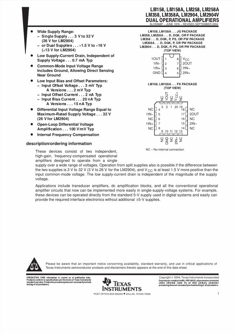
LM158, LM158A, LM258, LM258A LM3 58, LM3 58A, LM2904, LM2 904 V DUAL OPERA TIONAL AMPLI FIERS SLOS068P − JUNE 1976 − REVISED SEPTEMBER 2004 1 POST OFFICE BOX 655303 • DALLAS, TEXAS 75265 D Wide Supply Range: − Si ngle Supply ... 3 V to 32 V (26 V for LM2904) − or Dual Suppli es ... +1.5 V to +16 V (+13 V for LM2904) D Low Supply-Current Drain, Independent of Supply Vol tage . . . 0.7 mA Typ D Common-Mode Input Voltage Range Includes Ground, Allowing Direct Sensing Near Ground D Low Input Bias and Offset Parameters: − Input Offset V ol tage . . . 3 mV T yp A V er si ons . . . 2 mV T yp − Input Offset Current . . . 2 n A T yp − Input Bi as Curr ent... 20 nA T yp A V er sions . . . 15 nA T yp D Differential Input Voltage Range Equal to Maximum-Rated Supply V ol tage ... 32 V (26 V for L M2904) D Open-Loop Differential Voltage Amp lif ica ti on . . . 100 V/ mV T yp D Internal Frequency Compensation description /ordering information These devices consist of two independent, high-gain, frequency-compensated operational amplifiers designed to operate from a single supply over a wide range of voltages. Operation from split supplies also is possible if the difference between the two supplies is 3 V to 32 V (3 V to 26 V for the LM2904), and V CC is at least 1.5 V more positive than the input common-mode voltage. The low supply-current drain is independent of the magnitude of the supply voltage. Applications include transducer amplifiers, dc amplification blocks, and all the conventional operational amplifier circuits that now can be implemented more easily in single-supply-voltage systems. For example, these devices can be operated directly from the standard 5-V supply used in digital systems and easily can provide the required interface electronics without additional ±5-V supplies. Please be aware that an important notice concerning availability, standard warranty, and use in critical applications of T exas Instruments semiconductor produ cts and disclaimers thereto appears at the end of this data sheet. Copyright 2004, Texas Instruments Incorporated PR ODUC TI ON DATA in fo rmation is cu rrent as of publication da te. Prod ucts conform to speci ficatio ns per the terms of Tex as Instru ment s stand ard warra nty . Prod uctio n proce ssing does not necess arily include testin g of all parameters. 1 2 3 4 8 7 6 5 1OUT 1IN− 1IN+ GND V CC 2OUT 2IN− 2IN+ LM1 58, LM158A ... JG PACKAGE LM258, LM258A . . . D, DGK, OR P PACKAGE LM358 . . . D, DGK, P , PS, OR PW P ACK AGE LM358A. . . D, DGK, P, OR PW PACKAGE LM2904 . . . D, DGK, P , PS, OR PW PACKAGE (TOP VIEW) 3 2 1 20 19 9 10 11 12 13 4 5 6 7 8 18 17 16 15 14 NC 2OUT NC 2IN− NC NC 1IN− NC 1IN+ NC LM1 58, LM158A. .. FK PACKAGE (TOP VIEW) N C 1 O U T N C N C N C N C G N D N C C C + V 2 I N + NC − No internal connection On product s comp liant to MILPRF 38535, all parameters are tested un le ss ot he rwis e no te d. On al l ot he r pr od uc ts , pr od uc ti on proce ssing does not neces sarily include testing of all parameters.
Transcript of 0xdxyqz89u9xgdgs2o3yw6ocp6ky
8/3/2019 0xdxyqz89u9xgdgs2o3yw6ocp6ky
http://slidepdf.com/reader/full/0xdxyqz89u9xgdgs2o3yw6ocp6ky 1/21
LM158, LM158A, LM258, LM258ALM358, LM358A, LM2904, LM2904VDUAL OPERATIONAL AMPLIFIERS
SLOS068P − JUNE 1976 − REVISED SEPTEMBER 2004
1POST OFFICE BOX 655303 • DALLAS, TEXAS 75265
D Wide Supply Range:
− Single Supply . . . 3 V to 32 V(26 V for LM2904)
− or Dual Supplies . . . +1.5 V to +16 V(+13 V for LM2904)
D Low Supply-Current Drain, Independent of
Supply Voltage . . . 0.7 mA Typ
D Common-Mode Input Voltage RangeIncludes Ground, Allowing Direct SensingNear Ground
D Low Input Bias and Offset Parameters:− Input Offset Voltage . . . 3 mV Typ
A Versions . . . 2 mV Typ− Input Offset Current . . . 2 nA Typ− Input Bias Current . . . 20 nA Typ
A Versions . . . 15 nA Typ
D Differential Input Voltage Range Equal toMaximum-Rated Supply Voltage . . . 32 V
(26 V for LM2904)
D Open-Loop Differential Voltage
Amplification . . . 100 V/mV Typ
D Internal Frequency Compensation
description/ordering information
These devices consist of two independent,high-gain, frequency-compensated operationalamplifiers designed to operate from a singlesupply over a wide range of voltages. Operation from split supplies also is possible if the difference between
the two supplies is 3 V to 32 V (3 V to 26 V for the LM2904), and VCC is at least 1.5 V more positive than the
input common-mode voltage. The low supply-current drain is independent of the magnitude of the supplyvoltage.
Applications include transducer amplifiers, dc amplification blocks, and all the conventional operationalamplifier circuits that now can be implemented more easily in single-supply-voltage systems. For example,
these devices can be operated directly from the standard 5-V supply used in digital systems and easily canprovide the required interface electronics without additional ±5-V supplies.
Please be aware that an important notice concerning availability, standard warranty, and use in critical applications of
Texas Instruments semiconductor products and disclaimers thereto appears at the end of this data sheet.
Copyright 2004, Texas Instruments IncorporatedPRODUCTION DATA information is current as of publication date.Products conform to specifications per the terms of Texas Instrumentsstandard warranty. Production processing doesnot necessarilyincludetesting of all parameters.
12
3
4
87
6
5
1OUT1IN−
1IN+
GND
VCC2OUT
2IN−
2IN+
LM158, LM158A . . . JG PACKAGE
LM258, LM258A . . . D, DGK, OR P PACKAGE
LM358 . . . D, DGK, P, PS, OR PW PACKAGE
LM358A . . . D, DGK, P, OR PW PACKAGE
LM2904 . . . D, DGK, P, PS, OR PW PACKAGE
(TOP VIEW)
3 2 1 20 19
9 10 11 12 13
4
5
6
7
8
18
17
16
15
14
NC
2OUT
NC
2IN−
NC
NC
1IN−
NC
1IN+
NC
LM158, LM158A . . . FK PACKAGE
(TOP VIEW)
N C
1 O U T
N C
N C
N C
N C
G N D
N C
C C +
V
2 I N +
NC − No internal connection
Onproducts compliant toMILPRF38535, allparameters aretestedunless o therwise noted. On a ll o ther p roducts, p roductionprocessing doesnot necessarilyincludetestingof all parameters.
8/3/2019 0xdxyqz89u9xgdgs2o3yw6ocp6ky
http://slidepdf.com/reader/full/0xdxyqz89u9xgdgs2o3yw6ocp6ky 2/21
LM158, LM158A, LM258, LM258ALM358, LM358A, LM2904, LM2904VDUAL OPERATIONAL AMPLIFIERSSLOS068P − JUNE 1976 − REVISED SEPTEMBER 2004
2 POST OFFICE BOX 655303 • DALLAS, TEXAS 75265
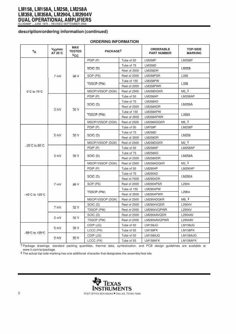
description/ordering information (continued)
ORDERING INFORMATION
TAVIOmax
AT 25°C
MAX
TESTED
VCC
PACKAGE† ORDERABLE
PART NUMBER
TOP-SIDE
MARKING
PDIP (P) Tube of 50 LM358P LM358P
Tube of 75 LM358D
SOIC (D)Reel of 2500 LM358DR
LM358
7 mV 30 V SOP (PS) Reel of 2000 LM358PSR L358
Tube of 150 LM358PWTSSOP (PW)
Reel of 2000 LM358PWRL358
0°C to 70°C MSOP/VSSOP (DGK) Reel of 2500 LM358DGKR M5_ ‡
PDIP (P) Tube of 50 LM358AP LM358AP
Tube of 75 LM358AD
SOIC (D)Reel of 2500 LM358ADR
LM358A
3 mV 30 V
Tube of 150 LM358APW
TSSOP (PW)Reel of 2000 LM358APWR
L358A
MSOP/VSSOP (DGK) Reel of 2500 LM358ADGKR M6_ ‡
PDIP (P) Tube of 50 LM258P LM258P
Tube of 75 LM258D
5 mV 30 V SOIC (D)Reel of 2500 LM258DR
LM258
MSOP/VSSOP (DGK) Reel of 2500 LM258DGKR M2_ ‡
−25°C to 85°CPDIP (P) Tube of 50 LM258AP LM258AP
Tube of 75 LM258AD
3 mV 30 V SOIC (D)Reel of 2500 LM258ADR
LM258A
MSOP/VSSOP (DGK) Reel of 2500 LM258ADGKR M3_ ‡
PDIP (P) Tube of 50 LM2904P LM2904P
Tube of 75 LM2904D
SOIC (D)Reel of 2500 LM2904DR
LM2904
7 mV 26 V SOP (PS) Reel of 2000 LM2904PSR L2904
Tube of 150 LM2904PW
−40°C to 125°CTSSOP (PW)
Reel of 2000 LM2904PWRL2904
MSOP/VSSOP (DGK) Reel of 2500 LM2904DGKR MB_ ‡
SOIC (D) Reel of 2500 LM2904VQDR L2904V
7 mV 32 VTSSOP (PW) Reel of 2000 LM2904VQPWR L2904V
SOIC (D) Reel of 2500 LM2904AVQDR L2904AV
2 mV 32 VTSSOP (PW) Reel of 2000 LM2904AVQPWR L2904AV
CDIP (JG) Tube of 50 LM158JG LM158JG
° °
5 mV 30 VLCCC (FK) Tube of 55 LM158FK LM158FK
−55°C to 125°C
CDIP (JG) Tube of 50 LM158AJG LM158AJG2 mV 30 V
LCCC (FK) Tube of 55 LM158AFK LM158AFK
† Package drawings, standard packing quantities, thermal data, symbolization, and PCB design guidelines are available at
www.ti.com/sc/package.‡ The actual top-side marking has one additional character that designates the assembly/test site.
8/3/2019 0xdxyqz89u9xgdgs2o3yw6ocp6ky
http://slidepdf.com/reader/full/0xdxyqz89u9xgdgs2o3yw6ocp6ky 3/21
LM158, LM158A, LM258, LM258ALM358, LM358A, LM2904, LM2904VDUAL OPERATIONAL AMPLIFIERS
SLOS068P − JUNE 1976 − REVISED SEPTEMBER 2004
3POST OFFICE BOX 655303 • DALLAS, TEXAS 75265
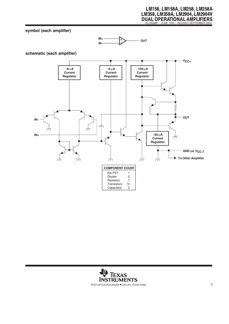
symbol (each amplifier)
IN+
IN−OUT+
−
schematic (each amplifier)
VCC+
OUT
GND (or VCC−)
To Other Amplifier
IN−
IN+
≈6-µA
Current
Regulator
≈6-µA
Current
Regulator
≈100-µA
Current
Regulator
≈50-µA
Current
Regulator
Epi-FET
Diodes
Resistors
Transistors
Capacitors
COMPONENT COUNT
1
2
7
51
2
8/3/2019 0xdxyqz89u9xgdgs2o3yw6ocp6ky
http://slidepdf.com/reader/full/0xdxyqz89u9xgdgs2o3yw6ocp6ky 4/21
LM158, LM158A, LM258, LM258ALM358, LM358A, LM2904, LM2904VDUAL OPERATIONAL AMPLIFIERSSLOS068P − JUNE 1976 − REVISED SEPTEMBER 2004
4 POST OFFICE BOX 655303 • DALLAS, TEXAS 75265
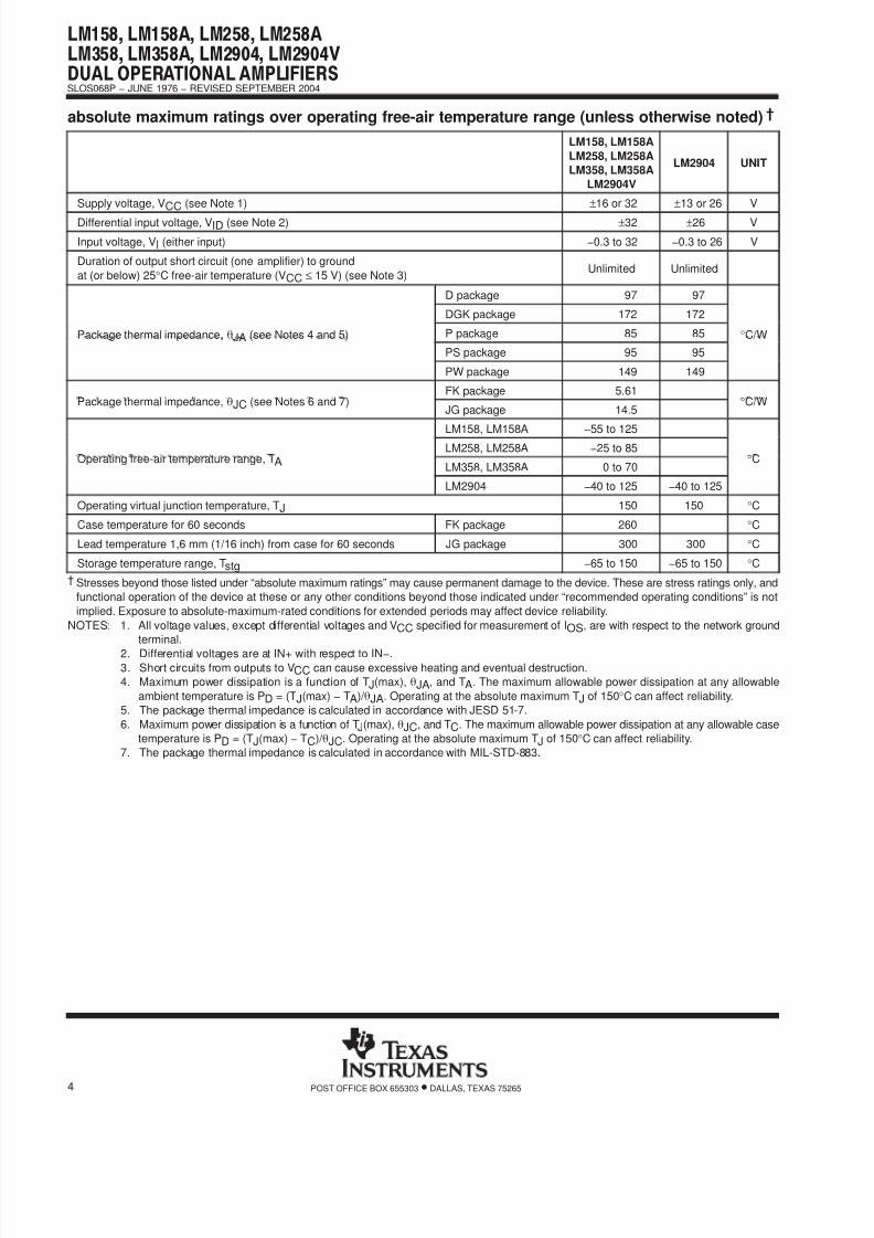
absolute maximum ratings over operating free-air temperature range (unless otherwise noted)†
LM158, LM158A
LM258, LM258A
LM358, LM358A
LM2904V
LM2904 UNIT
Supply voltage, VCC (see Note 1) ±16 or 32 ±13 or 26 V
Differential input voltage, VID (see Note 2) ±32 ±26 V
Input voltage, VI (either input) −0.3 to 32 −0.3 to 26 V
Duration of output short circuit (one amplifier) to ground
at (or below) 25°C free-air temperature (VCC ≤ 15 V) (see Note 3)Unlimited Unlimited
D package 97 97
DGK package 172 172
Package thermal impedance, qJA (see Notes 4 and 5) P package 85 85 °C/W,
PS package 95 95
PW package 149 149
FK package 5.61
Package thermal impedance, qJC (see Notes 6 and 7)JG package 14.5
°C/W
LM158, LM158A −55 to 125
LM258, LM258A −25 to 85
Operating free-air temperature range, TA LM358, LM358A 0 to 70°C
LM2904 −40 to 125 −40 to 125
Operating virtual junction temperature, TJ 150 150 °C
Case temperature for 60 seconds FK package 260 °C
Lead temperature 1,6 mm (1/16 inch) from case for 60 seconds JG package 300 300 °C
Storage temperature range, Tstg −65 to 150 −65 to 150 °C
† Stresses beyond those listed under “absolute maximum ratings” may cause permanent damage to the device. These are stress ratings only, and
functional operation of the device at these or any other conditions beyond those indicated under “recommended operating conditions” is not
implied. Exposure to absolute-maximum-rated conditions for extended periods may affect device reliability.
NOTES: 1. All voltage values, except differential voltages and VCC specified for measurement of IOS, are with respect to the network ground
terminal.
2. Differential voltages are at IN+ with respect to IN−.3. Short circuits from outputs to VCC can cause excessive heating and eventual destruction.
4. Maximum power dissipation is a function of TJ(max), qJA, and TA. The maximum allowable power dissipation at any allowable
ambient temperature is PD = (TJ(max) − TA)/ qJA. Operating at the absolute maximum TJ of 150°C can affect reliability.
5. The package thermal impedance is calculated in accordance with JESD 51-7.
6. Maximum power dissipation is a function of TJ(max), qJC, and TC. The maximum allowable power dissipation at any allowable case
temperature is PD = (TJ(max) − TC)/ qJC. Operating at the absolute maximum TJ of 150°C can affect reliability.
7. The package thermal impedance is calculated in accordance with MIL-STD-883.
8/3/2019 0xdxyqz89u9xgdgs2o3yw6ocp6ky
http://slidepdf.com/reader/full/0xdxyqz89u9xgdgs2o3yw6ocp6ky 5/21
LM158, LM158A, LM258, LM258ALM358, LM358A, LM2904, LM2904VDUAL OPERATIONAL AMPLIFIERS
SLOS068P − JUNE 1976 − REVISED SEPTEMBER 2004
5POST OFFICE BOX 655303 • DALLAS, TEXAS 75265
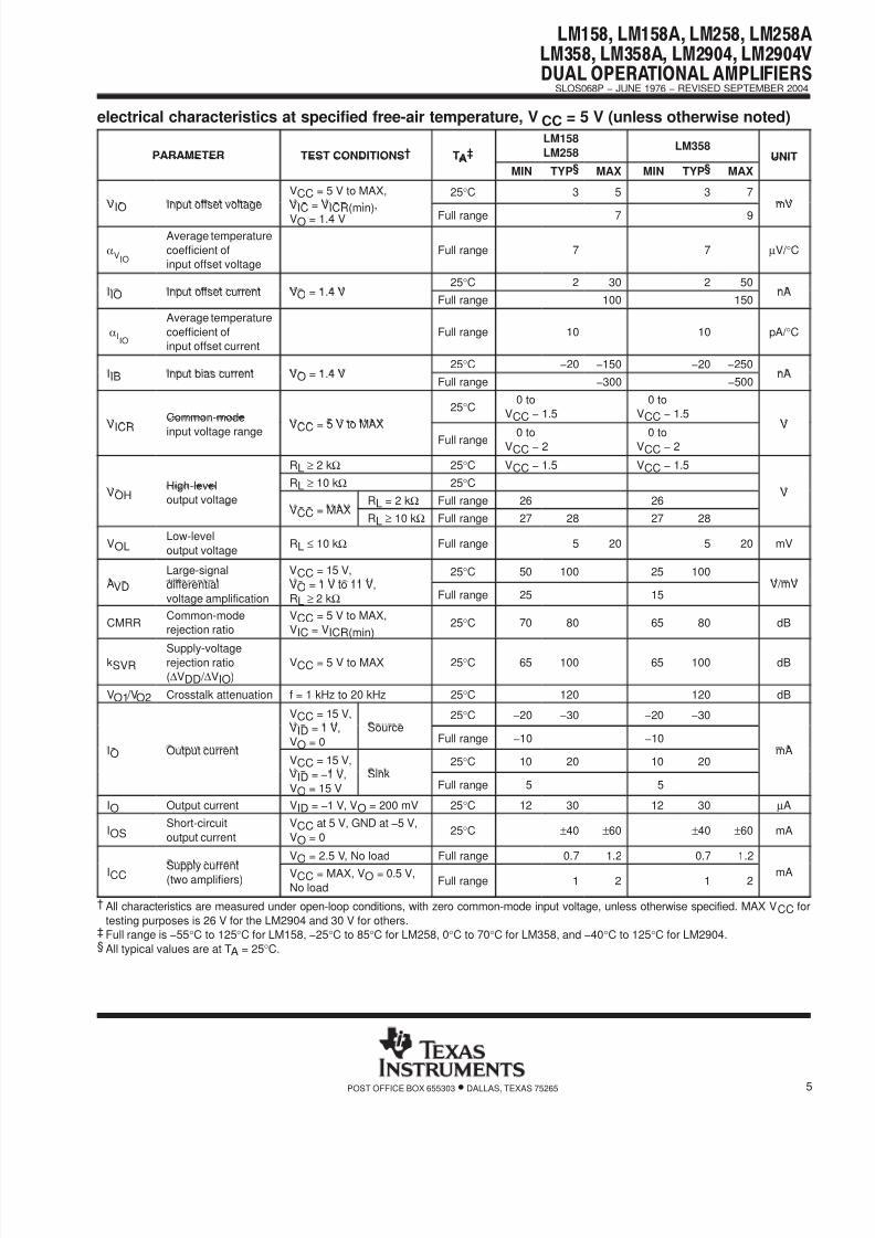
electrical characteristics at specified free-air temperature, VCC = 5 V (unless otherwise noted)
PARAMETER TEST CONDITIONS† TA‡
LM158
LM258LM358
UNIT
MIN TYP§ MAX MIN TYP§ MAX
VCC = 5 V to MAX,
25°C 3 5 3 7
VIO Input offset voltage VIC = VICR(min),
VO = 1.4 V Full range 7 9
mV
aVIO
Average temperature
coefficient of
input offset voltage
Full range 7 7 µV/ °C
25°C 2 30 2 50
IIO Input offset current VO = 1.4 VFull range 100 150
nA
aIIO
Average temperature
coefficient of
input offset current
Full range 10 10 pA/ °C
25°C −20 −150 −20 −250
IIB Input bias current VO = 1.4 VFull range −300 −500
nA
Common-mode
25°C0 to
VCC − 1.5
0 to
VCC − 1.5VICR
input voltage range
VCC = 5 V to MAX
Full range 0 toVCC − 2
0 toVCC − 2
V
RL ≥ 2 kΩ 25°C VCC − 1.5 VCC − 1.5
High-level RL ≥ 10 kΩ 25°CVOH output voltage
RL = 2 kΩ Full range 26 26
V
VCC = MAXRL ≥ 10 kΩ Full range 27 28 27 28
VOLLow-level
output voltageRL ≤ 10 kΩ Full range 5 20 5 20 mV
Large-signal VCC = 15 V, 25°C 50 100 25 100AVD differential
voltage amplification
VO = 1 V to 11 V,
RL ≥ 2 kΩ Full range 25 15V/mV
CMRRCommon-mode
rejection ratio
VCC = 5 V to MAX,
VIC = VICR(min)25°C 70 80 65 80 dB
kSVRSupply-voltagerejection ratio
(∆VDD / ∆VIO)
VCC = 5 V to MAX 25°C 65 100 65 100 dB
VO1 /VO2 Crosstalk attenuation f = 1 kHz to 20 kHz 25°C 120 120 dB
VCC = 15 V,
25°C −20 −30 −20 −30
VID = 1 V,
VO = 0
SourceFull range −10 −10
IO Output currentVCC = 15 V,
25°C 10 20 10 20
mA
VID = −1 V,
VO = 15 V
SinkFull range 5 5
IO Output current VID = −1 V, VO = 200 mV 25°C 12 30 12 30 µA
IOSShort-circuit
output current
VCC at 5 V, GND at −5 V,
VO = 025°C ±40 ±60 ±40 ±60 mA
VO = 2.5 V, No load Full range 0.7 1.2 0.7 1.2
ICC Supply current(two amplifiers)
VCC = MAX, VO = 0.5 V,
No loadFull range 1 2 1 2
mA
† All characteristics are measured under open-loop conditions, with zero common-mode input voltage, unless otherwise specified. MAX VCC for
testing purposes is 26 V for the LM2904 and 30 V for others.‡ Full range is −55°C to 125°C for LM158, −25°C to 85°C for LM258, 0°C to 70°C for LM358, and −40°C to 125°C for LM2904.§ All typical values are at TA = 25°C.
8/3/2019 0xdxyqz89u9xgdgs2o3yw6ocp6ky
http://slidepdf.com/reader/full/0xdxyqz89u9xgdgs2o3yw6ocp6ky 6/21
LM158, LM158A, LM258, LM258ALM358, LM358A, LM2904, LM2904VDUAL OPERATIONAL AMPLIFIERSSLOS068P − JUNE 1976 − REVISED SEPTEMBER 2004
6 POST OFFICE BOX 655303 • DALLAS, TEXAS 75265
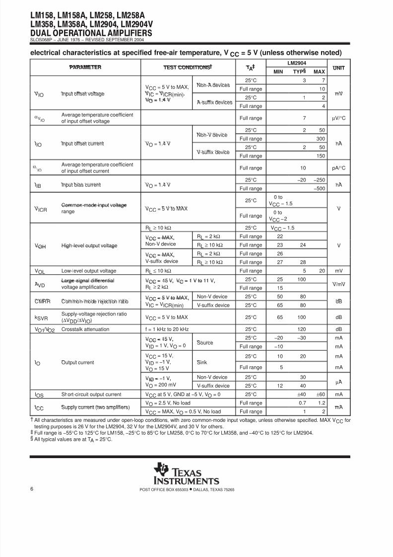
electrical characteristics at specified free-air temperature, VCC = 5 V (unless otherwise noted)
LM2904
PARAMETER TEST CONDITIONS TAMIN TYP§ MAX
UNIT
25°C 3 7
VCC = 5 V to MAX,
Non-A devicesFull range 10
VIO
Input offset voltage VIC = VICR(min),
V = 1.4 V
25°C 1 2mV
O = .A-suffix devices
Full range 4
aVIO
Average temperature coefficient
of input offset voltageFull range 7 µV/ °C
25°C 2 50
Non-V deviceFull range 300
IIO Input offset current VO = 1.4 V
25°C 2 50
nA
V-suffix deviceFull range 150
aIIO
Average temperature coefficient
of input offset currentFull range 10 pA/ °C
25°C −20 −250
IIB Input bias current VO = 1.4 VFull range −500
nA
Common-mode input voltage
25°C0 to
VCC − 1.5VICR
rangeVCC = 5 V to MAX
Full range0 to
VCC − 2
V
RL ≥ 10 kΩ 25°C VCC − 1.5
VCC = MAX, RL = 2 kΩ Full range 22
VOH High-level output voltage
,
Non-V device RL ≥ 10 kΩ Full range 23 24 V
VCC = MAX, RL = 2 kΩ Full range 26,
V-suffix device RL ≥ 10 kΩ Full range 27 28
VOL Low-level output voltage RL ≤ 10 kΩ Full range 5 20 mV
Large-signal differential VCC = 15 V, VO = 1 V to 11 V, 25°C 25 100AVD
voltage amplification
, ,
RL ≥ 2 kΩ Full range 15V/mV
VCC = 5 V to MAX, Non-V device 25°C 50 80
CMRR Common-mode rejection ratio,
VIC = VICR(min) V-suffix device 25°C 65 80dB
kSVRSupply-voltage rejection ratio
(∆VDD / ∆VIO)VCC = 5 V to MAX 25°C 65 100 dB
VO1 /VO2 Crosstalk attenuation f = 1 kHz to 20 kHz 25°C 120 dB
VCC = 15 V, 25°C −20 −30 mA,
VID = 1 V, VO = 0Source
Full range −10 mA
VCC = 15 V,
25°C 10 20 mA
IO Output current VID = −1 V,
VO = 15 VSink
Full range 5 mA
VID = −1 V, Non-V device 25°C 30,
VO = 200 mV V-suffix device 25°C 12 40µA
IOS Short-circuit output current VCC at 5 V, GND at −5 V, VO = 0 25°C ±40 ±60 mA
VO = 2.5 V, No load Full range 0.7 1.2
ICC Supply current (two amplifiers)VCC = MAX, VO = 0.5 V, No load Full range 1 2
mA
† All characteristics are measured under open-loop conditions, with zero common-mode input voltage, unless otherwise specified. MAX VCC for
testing purposes is 26 V for the LM2904, 32 V for the LM2904V, and 30 V for others.‡ Full range is −55°C to 125°C for LM158, −25°C to 85°C for LM258, 0°C to 70°C for LM358, and −40°C to 125°C for LM2904.§ All typical values are at TA = 25°C.
8/3/2019 0xdxyqz89u9xgdgs2o3yw6ocp6ky
http://slidepdf.com/reader/full/0xdxyqz89u9xgdgs2o3yw6ocp6ky 7/21
LM158, LM158A, LM258, LM258ALM358, LM358A, LM2904, LM2904VDUAL OPERATIONAL AMPLIFIERS
SLOS068P − JUNE 1976 − REVISED SEPTEMBER 2004
7POST OFFICE BOX 655303 • DALLAS, TEXAS 75265
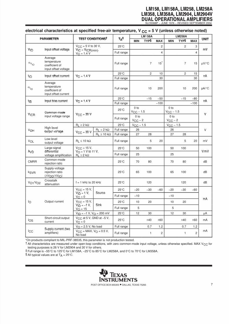
electrical characteristics at specified free-air temperature, VCC = 5 V (unless otherwise noted)
LM158A LM258A
PARAMETER TEST CONDITIONS TA MIN TYP§ MAX MIN TYP§ MAXUNIT
VCC = 5 V to 30 V,
25°C 2 2 3
VIO Input offset voltage VIC = VICR(min),
VO = 1.4 V Full range 4 4mV
aVIO
Averagetemperature
coefficient of
input offset voltage
Full range 7 15* 7 15 µV/ °C
25°C 2 10 2 15
IIO Input offset current VO = 1.4 VFull range 30 30
nA
aIIO
Average
temperature
coefficient of
input offset current
Full range 10 200 10 200 pA/ °C
25°C −15 −50 −15 −80
IIB Input bias current VO = 1.4 VFull range −100 −100
nA
Common-mode
25°C0 to
VCC
− 1.5
0 to
VCC
− 1.5VICR input voltage range VCC = 30 V
Full range0 to
VCC − 2
0 to
VCC − 2
V
RL ≥ 2 kΩ 25°C VCC − 1.5 VCC − 1.5
VOHHigh-level
RL = 2 kΩ Full range 26 26 V
ou pu vo age VCC = 30 VRL ≥ 10 kΩ Full range 27 28 27 28
VOLLow-level
output voltageRL ≤ 10 kΩ Full range 5 20 5 20 mV
Large-signal VCC = 15 V,
25°C 50 100 50 100
AVD differential
voltage amplification
VO = 1 V to 11 V,
RL ≥ 2 kΩ Full range 25 25V/mV
CMRRCommon-mode
rejection ratio25°C 70 80 70 80 dB
kSVR
Supply-voltage
rejection ratio
(∆VDD / ∆VIO)
25°C 65 100 65 100 dB
VO1 /VO2Crosstalk
attenuationf = 1 kHz to 20 kHz 25°C 120 120 dB
VCC = 15 V,
25°C −20 −30 −60 −20 −30 −60
VID = 1 V,
VO = 0
SourceFull range −10 −10
IO Output current VCC = 15 V,
25°C 10 20 10 20
mA
VID = −1 V,
VO = 15
SinkFull range 5 5
VID = −1 V, VO = 200 mV 25°C 12 30 12 30 µA
IOSShort-circuit output
current
VCC at 5 V, GND at −5 V,
VO = 025°C ±40 ±60 ±40 ±60 mA
VO = 2.5 V, No load Full range 0.7 1.2 0.7 1.2ICC
Supply current (two
amplifiers)VCC = MAX, VO = 0.5 V,
No loadFull range 1 2 1 2
mA
*On products compliant to MIL-PRF-38535, this parameter is not production tested.† All characteristics are measured under open-loop conditions, with zero common-mode input voltage, unless otherwise specified. MAX VCC for
testing purposes is 26 V for LM2904 and 30 V for others.‡ Full range is −55°C to 125°C for LM158A, −25°C to 85°C for LM258A, and 0°C to 70°C for LM358A.§ All typical values are at TA = 25°C.
8/3/2019 0xdxyqz89u9xgdgs2o3yw6ocp6ky
http://slidepdf.com/reader/full/0xdxyqz89u9xgdgs2o3yw6ocp6ky 8/21
LM158, LM158A, LM258, LM258ALM358, LM358A, LM2904, LM2904VDUAL OPERATIONAL AMPLIFIERSSLOS068P − JUNE 1976 − REVISED SEPTEMBER 2004
8 POST OFFICE BOX 655303 • DALLAS, TEXAS 75265
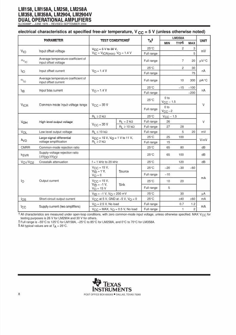
electrical characteristics at specified free-air temperature, VCC = 5 V (unless otherwise noted)
LM358A
PARAMETER TEST CONDITIONS TAMIN TYP§ MAX
UNIT
VCC = 5 V to 30 V, 25°C 2 3
VIO Input offset voltage,
VIC = VICR(min), VO = 1.4 V Full range 5mV
aVIO
Average temperature coefficient ofinput offset voltage
Full range 7 20 µV/ °C
25°C 2 30
IIO Input offset current VO = 1.4 VFull range 75
nA
aIIO
Average temperature coefficient of
input offset currentFull range 10 300 pA/ °C
25°C −15 −100
IIB Input bias current VO = 1.4 VFull range −200
nA
25°C0 to
VCC − 1.5VICR Common-mode input voltage range VCC = 30 V
Full range0 to
VCC − 2
V
RL ≥ 2 kΩ 25°C VCC − 1.5VOH High-level output voltage
RL = 2 kΩ Full range 26 V
VCC = 30 VRL ≥ 10 kΩ Full range 27 28
VOL Low-level output voltage RL ≤ 10 kΩ Full range 5 20 mV
Large-signal differential VCC = 15 V, VO = 1 V to 11 V, 25°C 25 100AVD
voltage amplification
, ,
RL ≥ 2 kΩ Full range 15V/mV
CMRR Common-mode rejection ratio 25°C 65 80 dB
kSVRSupply-voltage rejection ratio
(∆VDD / ∆VIO)25°C 65 100 dB
VO1 /VO2 Crosstalk attenuation f = 1 kHz to 20 kHz 25°C 120 dB
VCC = 15 V,
25°C −20 −30 −60
VID = 1 V,
VO = 0
Source
Full range −10IO Output current VCC = 15 V,
25°C 10 20
mA
VID = −1 V,
VO = 15 VSink
Full range 5
VID = −1 V, VO = 200 mV 25°C 30 µA
IOS Short-circuit output current VCC at 5 V, GND at −5 V, VO = 0 25°C ±40 ±60 mA
VO = 2.5 V, No load Full range 0.7 1.2
ICC Supply current (two amplifiers)VCC = MAX, VO = 0.5 V, No load Full range 1 2
mA
† All characteristics are measured under open-loop conditions, with zero common-mode input voltage, unless otherwise specified. MAX VCC for
testing purposes is 26 V for LM2904 and 30 V for others.‡ Full range is −55°C to 125°C for LM158A, −25°C to 85°C for LM258A, and 0°C to 70°C for LM358A.§ All typical values are at TA = 25°C.
8/3/2019 0xdxyqz89u9xgdgs2o3yw6ocp6ky
http://slidepdf.com/reader/full/0xdxyqz89u9xgdgs2o3yw6ocp6ky 9/21
LM158, LM158A, LM258, LM258ALM358, LM358A, LM2904, LM2904VDUAL OPERATIONAL AMPLIFIERS
SLOS068P − JUNE 1976 − REVISED SEPTEMBER 2004
9POST OFFICE BOX 655303 • DALLAS, TEXAS 75265
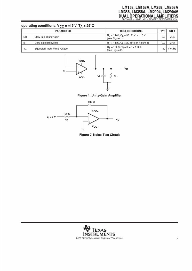
operating conditions, VCC = ±15 V, TA = 25°C
PARAMETER TEST CONDITIONS TYP UNIT
SR Slew rate at unity gainRL = 1 MΩ, CL = 30 pF, VI = ±10 V
(see Figure 1)0.3 V/ µs
B1 Unity-gain bandwidth RL = 1 MΩ, CL = 20 pF (see Figure 1) 0.7 MHz
Vn Equivalent input noise voltage RS = 100 Ω, VI = 0 V, f = 1 kHz(see Figure 2)
40 nV/ √Hz
+
VO−
RLCL
VI
VCC+
VCC−
Figure 1. Unity-Gain Amplifier
−
+VO
100 ΩVCC+
VCC−
RS
900 Ω
VI = 0 V
Figure 2. Noise-Test Circuit
8/3/2019 0xdxyqz89u9xgdgs2o3yw6ocp6ky
http://slidepdf.com/reader/full/0xdxyqz89u9xgdgs2o3yw6ocp6ky 10/21
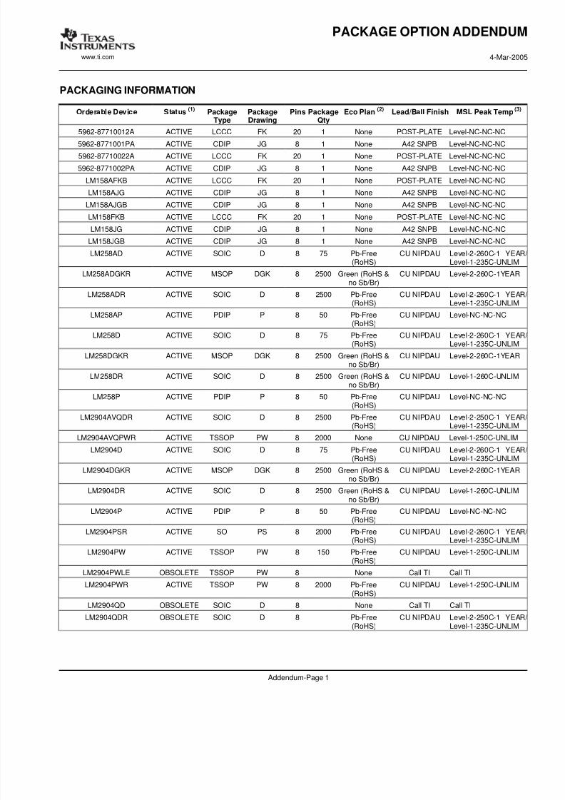
PACKAGING INFORMATION
Orderable Device Status (1) PackageType
PackageDrawing
Pins PackageQty
Eco Plan (2) Lead/Ball Finish MSL Peak Temp (3)
5962-87710012A ACTIVE LCCC FK 20 1 None POST-PLATE Level-NC-NC-NC
5962-8771001PA ACTIVE CDIP JG 8 1 None A42 SNPB Level-NC-NC-NC
5962-87710022A ACTIVE LCCC FK 20 1 None POST-PLATE Level-NC-NC-NC
5962-8771002PA ACTIVE CDIP JG 8 1 None A42 SNPB Level-NC-NC-NC
LM158AFKB ACTIVE LCCC FK 20 1 None POST-PLATE Level-NC-NC-NC
LM158AJG ACTIVE CDIP JG 8 1 None A42 SNPB Level-NC-NC-NC
LM158AJGB ACTIVE CDIP JG 8 1 None A42 SNPB Level-NC-NC-NC
LM158FKB ACTIVE LCCC FK 20 1 None POST-PLATE Level-NC-NC-NC
LM158JG ACTIVE CDIP JG 8 1 None A42 SNPB Level-NC-NC-NC
LM158JGB ACTIVE CDIP JG 8 1 None A42 SNPB Level-NC-NC-NC
LM258AD ACTIVE SOIC D 8 75 Pb-Free(RoHS)
CU NIPDAU Level-2-260C-1 YEAR/Level-1-235C-UNLIM
LM258ADGKR ACTIVE MSOP DGK 8 2500 Green (RoHS &
no Sb/Br)
CU NIPDAU Level-2-260C-1YEAR
LM258ADR ACTIVE SOIC D 8 2500 Pb-Free(RoHS)
CU NIPDAU Level-2-260C-1 YEAR/Level-1-235C-UNLIM
LM258AP ACTIVE PDIP P 8 50 Pb-Free(RoHS)
CU NIPDAU Level-NC-NC-NC
LM258D ACTIVE SOIC D 8 75 Pb-Free(RoHS)
CU NIPDAU Level-2-260C-1 YEAR/Level-1-235C-UNLIM
LM258DGKR ACTIVE MSOP DGK 8 2500 Green (RoHS &no Sb/Br)
CU NIPDAU Level-2-260C-1YEAR
LM258DR ACTIVE SOIC D 8 2500 Green (RoHS &no Sb/Br)
CU NIPDAU Level-1-260C-UNLIM
LM258P ACTIVE PDIP P 8 50 Pb-Free(RoHS)
CU NIPDAU Level-NC-NC-NC
LM2904AVQDR ACTIVE SOIC D 8 2500 Pb-Free(RoHS) CU NIPDAU Level-2-250C-1 YEAR/Level-1-235C-UNLIM
LM2904AVQPWR ACTIVE TSSOP PW 8 2000 None CU NIPDAU Level-1-250C-UNLIM
LM2904D ACTIVE SOIC D 8 75 Pb-Free(RoHS)
CU NIPDAU Level-2-260C-1 YEAR/Level-1-235C-UNLIM
LM2904DGKR ACTIVE MSOP DGK 8 2500 Green (RoHS &no Sb/Br)
CU NIPDAU Level-2-260C-1YEAR
LM2904DR ACTIVE SOIC D 8 2500 Green (RoHS &no Sb/Br)
CU NIPDAU Level-1-260C-UNLIM
LM2904P ACTIVE PDIP P 8 50 Pb-Free(RoHS)
CU NIPDAU Level-NC-NC-NC
LM2904PSR ACTIVE SO PS 8 2000 Pb-Free(RoHS)
CU NIPDAU Level-2-260C-1 YEAR/Level-1-235C-UNLIM
LM2904PW ACTIVE TSSOP PW 8 150 Pb-Free
(RoHS)
CU NIPDAU Level-1-250C-UNLIM
LM2904PWLE OBSOLETE TSSOP PW 8 None Call TI Call TI
LM2904PWR ACTIVE TSSOP PW 8 2000 Pb-Free(RoHS)
CU NIPDAU Level-1-250C-UNLIM
LM2904QD OBSOLETE SOIC D 8 None Call TI Call TI
LM2904QDR OBSOLETE SOIC D 8 Pb-Free(RoHS)
CU NIPDAU Level-2-250C-1 YEAR/Level-1-235C-UNLIM
PACKAGE OPTION ADDENDUM
www.ti.com 4-Mar-2005
Addendum-Page 1
8/3/2019 0xdxyqz89u9xgdgs2o3yw6ocp6ky
http://slidepdf.com/reader/full/0xdxyqz89u9xgdgs2o3yw6ocp6ky 11/21
Orderable Device Status (1) PackageType
PackageDrawing
Pins PackageQty
Eco Plan (2) Lead/Ball Finish MSL Peak Temp (3)
LM2904QP OBSOLETE PDIP P 8 None Call TI Call TI
LM2904VQDR ACTIVE SOIC D 8 2500 Pb-Free(RoHS)
CU NIPDAU Level-2-250C-1 YEAR/Level-1-235C-UNLIM
LM2904VQPWR ACTIVE TSSOP PW 8 2000 None CU NIPDAU Level-1-250C-UNLIM
LM358AD ACTIVE SOIC D 8 75 Pb-Free(RoHS)
CU NIPDAU Level-2-260C-1 YEAR/Level-1-235C-UNLIM
LM358ADGKR ACTIVE MSOP DGK 8 2500 Green (RoHS &no Sb/Br)
CU NIPDAU Level-2-260C-1YEAR
LM358ADR ACTIVE SOIC D 8 2500 Green (RoHS &no Sb/Br)
CU NIPDAU Level-1-260C-UNLIM
LM358AP ACTIVE PDIP P 8 50 Pb-Free(RoHS)
CU NIPDAU Level-NC-NC-NC
LM358APW ACTIVE TSSOP PW 8 150 Pb-Free(RoHS)
CU NIPDAU Level-1-250C-UNLIM
LM358APWR ACTIVE TSSOP PW 8 2000 Pb-Free(RoHS)
CU NIPDAU Level-1-250C-UNLIM
LM358D ACTIVE SOIC D 8 75 Green (RoHS &no Sb/Br)
CU NIPDAU Level-1-260C-UNLIM
LM358DGKR ACTIVE MSOP DGK 8 2500 Green (RoHS &no Sb/Br)
CU NIPDAU Level-2-260C-1YEAR
LM358DR ACTIVE SOIC D 8 2500 Green (RoHS &no Sb/Br)
CU NIPDAU Level-1-260C-UNLIM
LM358P ACTIVE PDIP P 8 50 Pb-Free(RoHS)
CU NIPDAU Level-NC-NC-NC
LM358PSLE OBSOLETE SO PS 8 None Call TI Call TI
LM358PSR ACTIVE SO PS 8 2000 Pb-Free(RoHS)
CU NIPDAU Level-2-260C-1 YEAR/Level-1-235C-UNLIM
LM358PW ACTIVE TSSOP PW 8 150 Pb-Free(RoHS)
CU NIPDAU Level-1-250C-UNLIM
LM358PWLE OBSOLETE TSSOP PW 8 None Call TI Call TI
LM358PWR ACTIVE TSSOP PW 8 2000 Pb-Free(RoHS)
CU NIPDAU Level-1-250C-UNLIM
(1) The marketing status values are defined as follows:ACTIVE: Product device recommended for new designs.LIFEBUY: TI has announced that the device will be discontinued, and a lifetime-buy period is in effect.NRND: Not recommended for new designs. Device is in production to support existing customers, but TI does not recommend using this part ina new design.PREVIEW: Device has been announced but is not in production. Samples may or may not be available.OBSOLETE: TI has discontinued the production of the device.
(2) Eco Plan - May not be currently available - please check http://www.ti.com/productcontent for the latest availability information and additionalproduct content details.None: Not yet available Lead (Pb-Free).Pb-Free (RoHS): TI's terms "Lead-Free" or "Pb-Free" mean semiconductor products that are compatible with the current RoHS requirementsfor all 6 substances, including the requirement that lead not exceed 0.1% by weight in homogeneous materials. Where designed to be solderedat high temperatures, TI Pb-Free products are suitable for use in specified lead-free processes.Green (RoHS & no Sb/Br): TI defines "Green" to mean "Pb-Free" and in addition, uses package materials that do not contain halogens,including bromine (Br) or antimony (Sb) above 0.1% of total product weight.
(3) MSL, Peak Temp. -- The Moisture Sensitivity Level rating according to the JEDECindustry standard classifications, and peak soldertemperature.
Important Information and Disclaimer:The information provided on this page represents TI's knowledge and belief as of the date that it is
PACKAGE OPTION ADDENDUM
www.ti.com 4-Mar-2005
Addendum-Page 2
8/3/2019 0xdxyqz89u9xgdgs2o3yw6ocp6ky
http://slidepdf.com/reader/full/0xdxyqz89u9xgdgs2o3yw6ocp6ky 12/21
provided. TI bases its knowledge and belief on information provided by third parties, and makes no representation or warranty as to theaccuracy of such information. Efforts are underway to better integrate information from third parties. TI has taken and continues to takereasonable steps to provide representative and accurate information but may not have conducted destructive testing or chemical analysis onincoming materials and chemicals. TI and TI suppliers consider certain information to be proprietary, and thus CAS numbers and other limitedinformation may not be available for release.
In no event shall TI's liability arising out of such information exceed the total purchase price of the TI part(s) at issue in this document sold by TIto Customer on an annual basis.
PACKAGE OPTION ADDENDUM
www.ti.com 4-Mar-2005
Addendum-Page 3
8/3/2019 0xdxyqz89u9xgdgs2o3yw6ocp6ky
http://slidepdf.com/reader/full/0xdxyqz89u9xgdgs2o3yw6ocp6ky 13/21
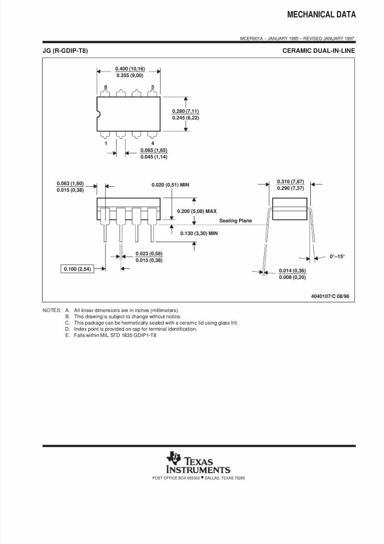
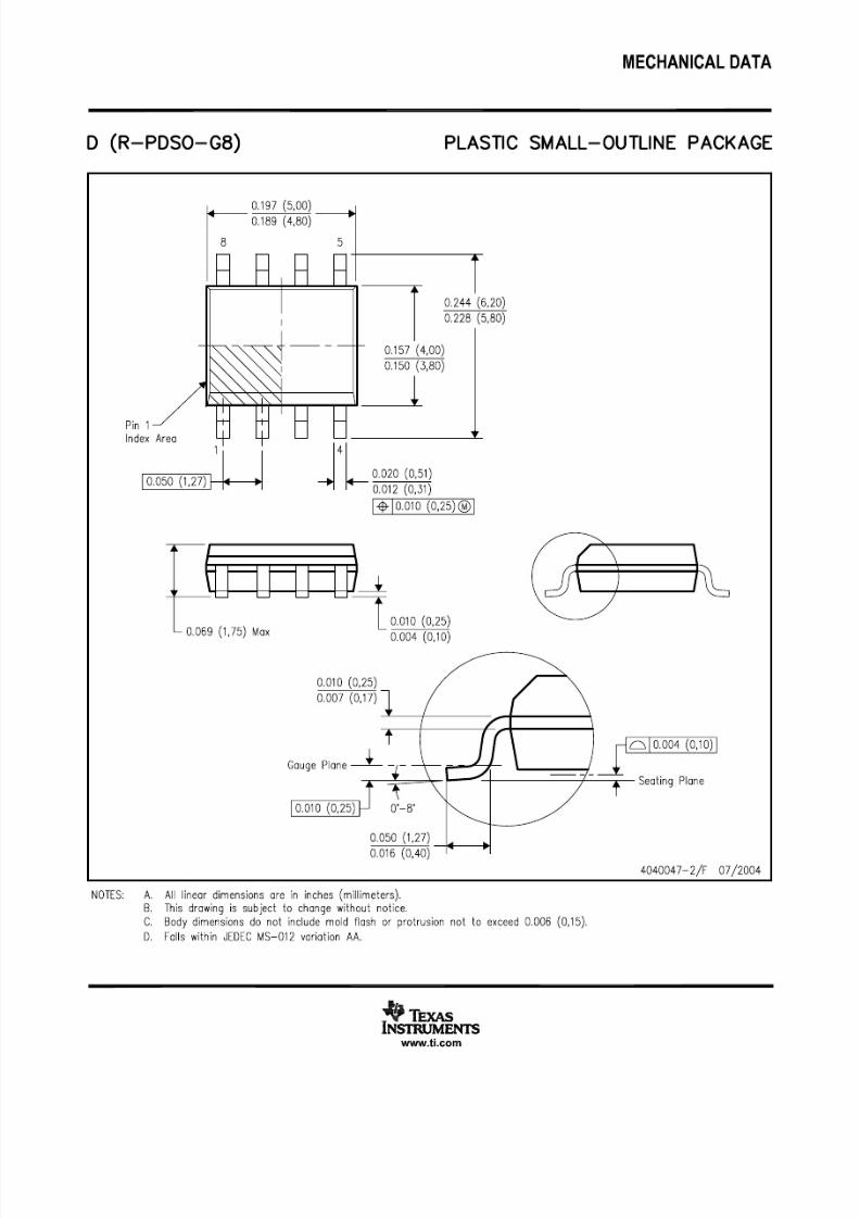
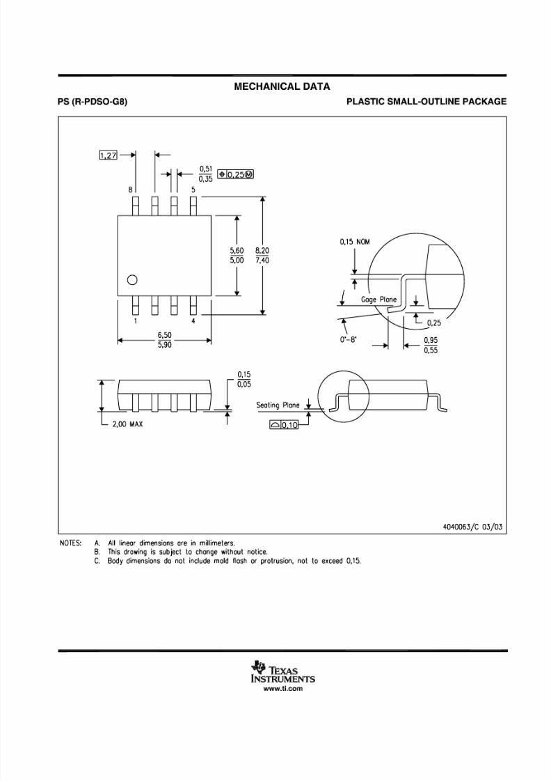
MECHANICAL DATA
MCER001A – JANUARY 1995 – REVISED JANUARY 1997
POST OFFICE BOX 655303 • DALLAS, TEXAS 75265
JG (R-GDIP-T8) CERAMIC DUAL-IN-LINE
0.310 (7,87)
0.290 (7,37)
0.014 (0,36)
0.008 (0,20)
Seating Plane
4040107/C 08/96
5
4
0.065 (1,65)
0.045 (1,14)
8
1
0.020 (0,51) MIN
0.400 (10,16)
0.355 (9,00)
0.015 (0,38)
0.023 (0,58)
0.063 (1,60)
0.015 (0,38)
0.200 (5,08) MAX
0.130 (3,30) MIN
0.245 (6,22)
0.280 (7,11)
0.100 (2,54)
0° –15°
NOTES: A. All linear dimensions are in inches (millimeters).
B. This drawing is subject to change without notice.
C. This package can be hermetically sealed with a ceramic lid using glass frit.
D. Index point is provided on cap for terminal identification.
E. Falls within MIL STD 1835 GDIP1-T8
8/3/2019 0xdxyqz89u9xgdgs2o3yw6ocp6ky
http://slidepdf.com/reader/full/0xdxyqz89u9xgdgs2o3yw6ocp6ky 14/21
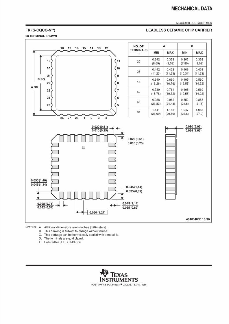
MECHANICAL DATA
MLCC006B – OCTOBER 1996
POST OFFICE BOX 655303 • DALLAS, TEXAS 75265
FK (S-CQCC-N**) LEADLESS CERAMIC CHIP CARRIER
4040140/ D 10/96
28 TERMINAL SHOWN
B
0.358
(9,09)
MAX
(11,63)
0.560
(14,22)
0.560
0.458
0.858
(21,8)
1.063
(27,0)
(14,22)
ANO. OF
MINMAX
0.358
0.660
0.761
0.458
0.342
(8,69)
MIN
(11,23)
(16,26)
0.640
0.739
0.442
(9,09)
(11,63)
(16,76)
0.962
1.165
(23,83)
0.938
(28,99)
1.141
(24,43)
(29,59)
(19,32)(18,78)
**
20
28
52
44
68
84
0.020 (0,51)
TERMINALS
0.080 (2,03)
0.064 (1,63)
(7,80)
0.307
(10,31)
0.406
(12,58)
0.495
(12,58)
0.495
(21,6)
0.850
(26,6)
1.047
0.045 (1,14)
0.045 (1,14)
0.035 (0,89)
0.035 (0,89)
0.010 (0,25)
121314151618 17
11
10
8
9
7
5
432
0.020 (0,51)
0.010 (0,25)
6
12826 27
19
21
B SQ
A SQ
22
23
24
25
20
0.055 (1,40)
0.045 (1,14)
0.028 (0,71)
0.022 (0,54)
0.050 (1,27)
NOTES: A. All linear dimensions are in inches (millimeters).B. This drawing is subject to change without notice.
C. This package can be hermetically sealed with a metal lid.
D. The terminals are gold plated.
E. Falls within JEDEC MS-004
8/3/2019 0xdxyqz89u9xgdgs2o3yw6ocp6ky
http://slidepdf.com/reader/full/0xdxyqz89u9xgdgs2o3yw6ocp6ky 15/21
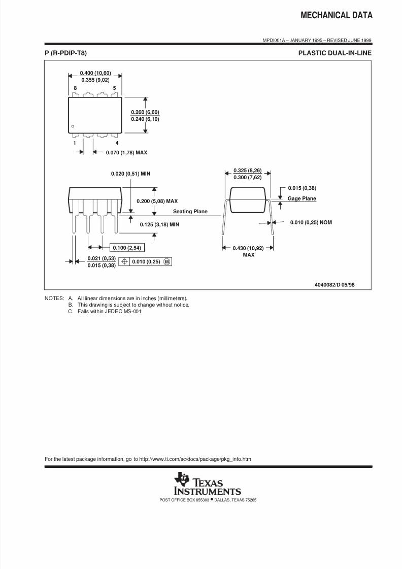
MECHANICAL DATA
MPDI001A – JANUARY 1995 – REVISED JUNE 1999
POST OFFICE BOX 655303 • DALLAS, TEXAS 75265
P (R-PDIP-T8) PLASTIC DUAL-IN-LINE
8
4
0.015 (0,38)
Gage Plane
0.325 (8,26)
0.300 (7,62)
0.010 (0,25) NOM
MAX
0.430 (10,92)
4040082/D 05/98
0.200 (5,08) MAX
0.125 (3,18) MIN
5
0.355 (9,02)
0.020 (0,51) MIN
0.070 (1,78) MAX
0.240 (6,10)
0.260 (6,60)
0.400 (10,60)
1
0.015 (0,38)
0.021 (0,53)
Seating Plane
M0.010 (0,25)
0.100 (2,54)
NOTES: A. All linear dimensions are in inches (millimeters).B. This drawing is subject to change without notice.
C. Falls within JEDEC MS-001
For the latest package information, go to http://www.ti.com/sc/docs/package/pkg_info.htm
8/3/2019 0xdxyqz89u9xgdgs2o3yw6ocp6ky
http://slidepdf.com/reader/full/0xdxyqz89u9xgdgs2o3yw6ocp6ky 16/21
8/3/2019 0xdxyqz89u9xgdgs2o3yw6ocp6ky
http://slidepdf.com/reader/full/0xdxyqz89u9xgdgs2o3yw6ocp6ky 17/21
8/3/2019 0xdxyqz89u9xgdgs2o3yw6ocp6ky
http://slidepdf.com/reader/full/0xdxyqz89u9xgdgs2o3yw6ocp6ky 18/21
8/3/2019 0xdxyqz89u9xgdgs2o3yw6ocp6ky
http://slidepdf.com/reader/full/0xdxyqz89u9xgdgs2o3yw6ocp6ky 19/21
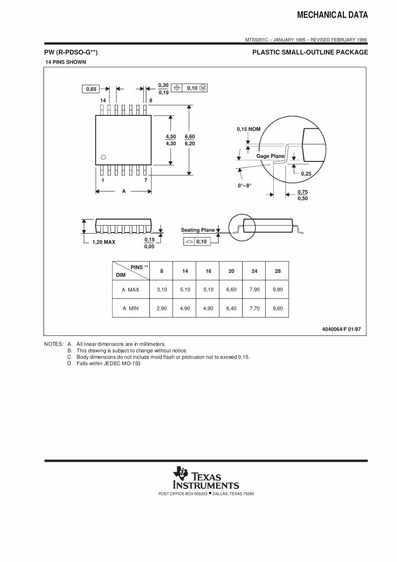
MECHANICAL DATA
MTSS001C – JANUARY 1995 – REVISED FEBRUARY 1999
POST OFFICE BOX 655303 • DALLAS, TEXAS 75265
PW (R-PDSO-G**) PLASTIC SMALL-OUTLINE PACKAGE
14 PINS SHOWN
0,65 M0,10
0,10
0,25
0,50
0,75
0,15 NOM
Gage Plane
28
9,80
9,60
24
7,90
7,70
2016
6,60
6,40
4040064/F 01/97
0,30
6,60
6,20
8
0,19
4,30
4,50
7
0,15
14
A
1
1,20 MAX
14
5,10
4,90
8
3,10
2,90
A MAX
A MIN
DIM
PINS **
0,05
4,90
5,10
Seating Plane
0° –8°
NOTES: A. All linear dimensions are in millimeters.
B. This drawing is subject to change without notice.
C. Body dimensions do not include mold flash or protrusion not to exceed 0,15.
D. Falls within JEDEC MO-153
8/3/2019 0xdxyqz89u9xgdgs2o3yw6ocp6ky
http://slidepdf.com/reader/full/0xdxyqz89u9xgdgs2o3yw6ocp6ky 20/21
IMPORTANT NOTICE
Texas Instruments Incorporated and its subsidiaries (TI) reserve the right to make corrections, modifications,
enhancements, improvements, and other changes to its products and services at any time and to discontinue
any product or service without notice. Customers should obtain the latest relevant information before placing
orders and should verify that such information is current and complete. All products are sold subject to TI’s terms
and conditions of sale supplied at the time of order acknowledgment.
TI warrants performance of its hardware products to the specifications applicable at the time of sale in
accordance with TI’s standard warranty. Testing and other quality control techniques are used to the extent TI
deems necessary to support this warranty. Except where mandated by government requirements, testing of all
parameters of each product is not necessarily performed.
TI assumes no liability for applications assistance or customer product design. Customers are responsible for
their products and applications using TI components. To minimize the risks associated with customer products
and applications, customers should provide adequate design and operating safeguards.
TI does not warrant or represent that any license, either express or implied, is granted under any TI patent right,
copyright, mask work right, or other TI intellectual property right relating to any combination, machine, or process
in which TI products or services are used. Information published by TI regarding third-party products or services
does not constitute a license from TI to use such products or services or a warranty or endorsement thereof.Use of such information may require a license from a third party under the patents or other intellectual property
of the third party, or a license from TI under the patents or other intellectual property of TI.
Reproduction of information in TI data books or data sheets is permissible only if reproduction is without
alteration and is accompanied by all associated warranties, conditions, limitations, and notices. Reproduction
of this information with alteration is an unfair and deceptive business practice. TI is not responsible or liable for
such altered documentation.
Resale of TI products or services with statements different from or beyond the parameters stated by TI for that
product or service voids all express and any implied warranties for the associated TI product or service and
is an unfair and deceptive business practice. TI is not responsible or liable for any such statements.
Following are URLs where you can obtain information on other Texas Instruments products and application
solutions:
Products Applications
Amplifiers amplifier.ti.com Audio www.ti.com/audio
Data Converters dataconverter.ti.com Automotive www.ti.com/automotive
DSP dsp.ti.com Broadband www.ti.com/broadband
Interface interface.ti.com Digital Control www.ti.com/digitalcontrol
Logic logic.ti.com Military www.ti.com/military
Power Mgmt power.ti.com Optical Networking www.ti.com/opticalnetwork
Microcontrollers microcontroller.ti.com Security www.ti.com/security
Telephony www.ti.com/telephony
Video & Imaging www.ti.com/video
Wireless www.ti.com/wireless
Mailing Address: Texas Instruments
Post Office Box 655303 Dallas, Texas 75265
Copyright 2005, Texas Instruments Incorporated

8/3/2019 0xdxyqz89u9xgdgs2o3yw6ocp6ky
http://slidepdf.com/reader/full/0xdxyqz89u9xgdgs2o3yw6ocp6ky 21/21
This datasheet has been download from:
www.datasheetcatalog.com
Datasheets for electronics components.


