0910 21 IEUVI Presentation outeuvlsymposium.lbl.gov/pdf/2009/pres/O_DI2-01_Gargini_Intel.pdf ·...
47
1 IEUVI Update EUVL Symposium, Prague Oct 21, 2009 Paolo Gargini Chairman ITRS Chairman Technology Strategy Committee, SIA Director of Technology Strategy Intel Fellow IEEE Fellow And David Chan, Jacque Georger, Frank Goodwin, George Huang, Bryan Rice, Andrea Wüest, Stefan Wurm
Transcript of 0910 21 IEUVI Presentation outeuvlsymposium.lbl.gov/pdf/2009/pres/O_DI2-01_Gargini_Intel.pdf ·...

12009 EUVL Symposium
IEUVI UpdateEUVL Symposium, Prague
Oct 21, 2009
Paolo GarginiChairman ITRS
Chairman Technology Strategy Committee, SIADirector of Technology Strategy
Intel FellowIEEE Fellow
AndDavid Chan, Jacque Georger, Frank Goodwin,
George Huang, Bryan Rice, Andrea Wüest, Stefan Wurm

22009 EUVL Symposium
Outline• Background and ITRS Lithography• IEUVI Overview• Source TWG• Resist TWG• Mask TWG• EUV Mask Infrastructure Development• Summary

32009 EUVL Symposium
Outline• Background and ITRS Lithography• IEUVI Overview• Source TWG• Resist TWG• Mask TWG• EUV Mask Infrastructure Development• Summary

42009 EUVL Symposium
2009 ITRS
1991 Micro Tech 2000Workshop Report
1994NTRS1992NTRS 1997NTRS
Japan KoreaEurope Taiwan USA
http://www.itrs.net
2001ITRS1999ITRS1998ITRSUpdate
2000ITRSUpdate
2002ITRSUpdate 2003ITRS
2004ITRSUpdate
2006ITRSUpdate2005ITRS 2007ITRS 2008ITRS
Update 2009ITRS

52009 EUVL Symposium
2009 Litho ITRS Update

62009 EUVL Symposium
Litho Potential Solutions
– Work in Progress – NOT FOR PUBLICATION
July 2009

72009 EUVL Symposium
Lithography Potential Solutions 2009First Year of IC Production 2009 2010 2011 2012 2013 2014 2015 2016 2017 2018 2019 2020 2021 2022 2023 2024
DRAM ½ pitch (nm) (contacted) 52 45 40 36 32 28 25 23 20 18 16 14 13 11 10 9Flash ½ Pitch (nm) (un-contacted Poly)(f) 38 32 28 25 23 20 18 16 14 13 11 10 8.9 8.0 7.1 6.3
45 193 nm immersion with water
32 193 nm Immersion Double PatternEUV (DRAM / MPU)
22 EUV193 nm Immersion Double / Multiple PatternML2Imprint
No proven optical solution below this line
16 EUVInnovative 193nm immersion Multiple PatternML2ImprintDirected Self AssemblyInterference Lithography
11 EUVML2ImprintDirected Self AssemblyInterference Lithography
This legend indicates the time during which research, development, and qualification/pre-production should be taking place for the solution. Research RequiredDevelopment UnderwayQualification / Pre-ProductionContinuous Improvement
Narrow Options
Narrow Options
Narrow Options
Narrow Options
MPU / DRAM time line
Flash Time Line
[Source: 2009 ITRS Litho Chapter Tables Work in Progress, Sept, 2009]
September 2009

82009 EUVL Symposium
Potential Show Stoppers• Resist Limitations (Shot Noise, Photo
electron Blur), e.g. set upper limits on LER & Resolution.
• Cost of Ownership – all technologies• EUV Lithography
– Source availability at required power levels and life time.
– Mask Defects– EUV Mask Infrastructure (actinic inspection tools
for blank, patterned mask, mask review)

92009 EUVL Symposium
Complexity Level Keeps on Increasing• Update Lithographic Requirements
– Separate into DRAM, Flash, MPU
• Double patterning (at least 3 types of approaches)• Double Exposure (DE), Litho Process Litho Etch (LPLE)• DP of Uncorrelated Lines (trenches) / Correlated Lines (lines)• Double Patterning Spacer Technology
• Double exposure / patterning requires a complex set of parameters when different exposures are used to define single features

102009 EUVL Symposium
Litho Requirements Table 76a&b Lithography Technology Requirements—Near-term Years
Year of Production 2007 2008 2009 2010 2011 2012 2013
DRAM ½ pitch (nm) (contacted) 68 59 52 45 40 36 32DRAMDRAM ½ pitch (nm) 68 59 52 45 40 36 32CD control (3 sigma) (nm) [B] 7.1 6.2 5.4 4.7 4.2 3.7 3.3Contact in resist (nm) 75 65 57 50 44 39 35Contact after etch (nm) 68 59 52 45 40 36 32Overlay [A] (3 sigma) (nm) 13.6 11.9 10.3 9.0 8.0 7.1 6.4FlashFlash ½ pitch (nm) (un-contacted poly) 54 45 40 36 32 28 25CD control (3 sigma) (nm) [B] 5.6 4.7 4.2 3.7 3.3 2.9 2.6Contact in resist (nm) 59 49 44 39 35 31 28Contact after etch (nm) 54 45 40 36 32 28 25Overlay [A] (3 sigma) (nm) 17.7 14.8 13.2 11.8 10.5 9.4 8.3
MPU/ASIC Metal 1 (M1) ½ pitch (nm) 68 59 52 45 40 36 32MPU gate in resist (nm) 54 47 41 35 31 28 25MPU physical gate length (nm) * 32 29 27 24 22 20 18
Gate CD control (3 sigma) (nm) [B] ** 3.3 3.0 2.8 2.5 2.3 2.1 1.9Contact in resist (nm) 84 73 64 56 50 44 39Contact after etch (nm) 77 67 58 51 45 40 36Overlay [A] (3 sigma) (nm) 17 15 13 11 10.0 8.9 8.0
MPU

112009 EUVL Symposium
Outline• Background and ITRS Lithography• IEUVI Overview• Source TWG• Resist TWG• Mask TWG• EUV Mask Infrastructure Development• Summary

122009 EUVL Symposium
International EUV Initiative (IEUVI)…
Europe
United States
Asia / Pacific
• IMEC• LETI• MEDEA+, CATRENE• ENIAC, AENEAS
• EUVA• SELETE• ASET*
• SEMATECH• CNSE• SRC
IEUVI International
EUVInitiative
IEUVI Mission: To further the coordination of collaborative efforts among leading EUVL R&D consortia. http://www.ieuvi.org

132009 EUVL Symposium
IEUVI – What, How, and Who
• What: To address infrastructural issues that need to be resolved for EUVL commercialization.
• How: The IEUVI collects technical inputs through its Technical Working Groups (TWGs), and identifies possible show stoppers for commercialization.
• Who: IEUVI TWG members include integrated device manufacturers, suppliers, national laboratories and universities.
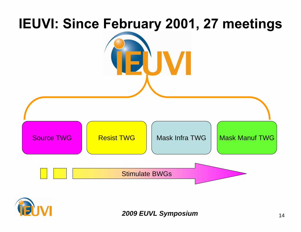
142009 EUVL Symposium
Source TWG Resist TWG Mask Infra TWG Mask Manuf TWG
Stimulate BWGs
IEUVI: Since February 2001, 27 meetings
152009 EUVL Symposium
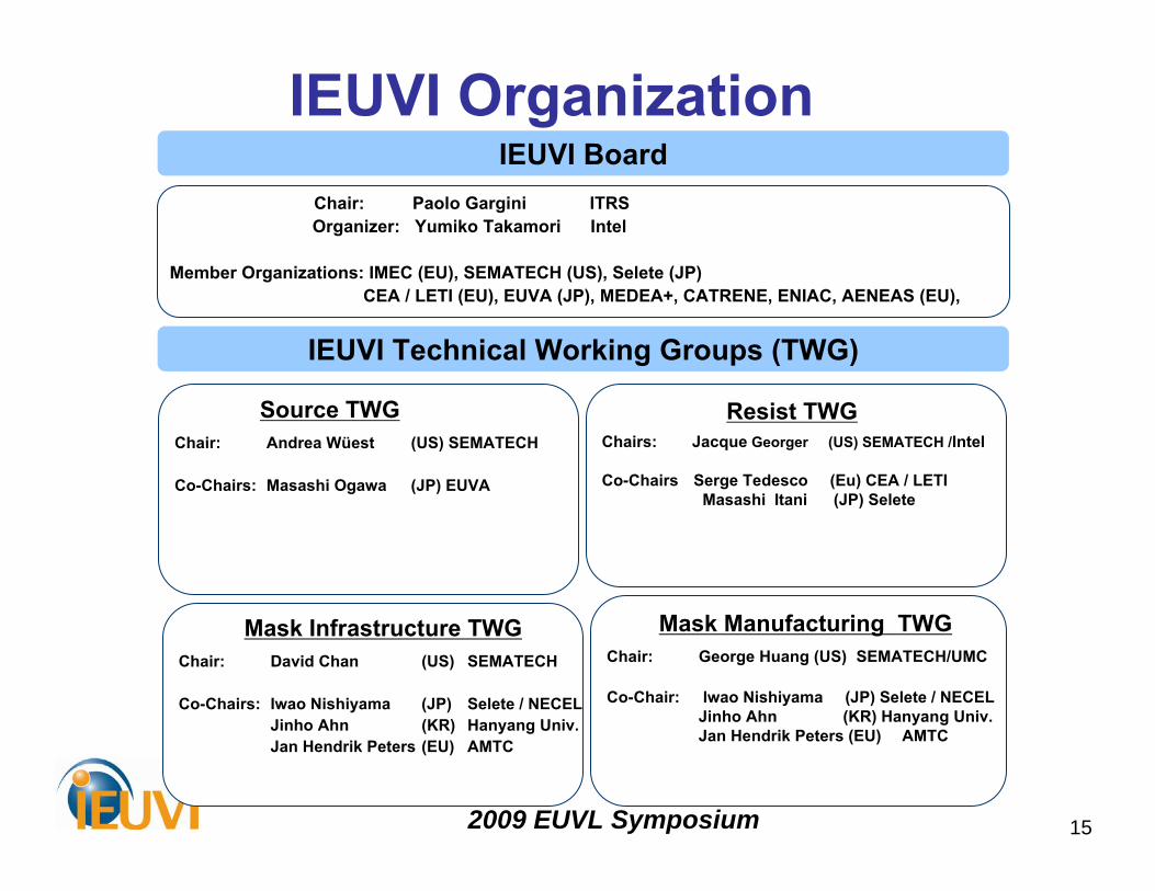
Mask Infrastructure TWGChair: David Chan (US) SEMATECH
Co-Chairs: Iwao Nishiyama (JP) Selete / NECELJinho Ahn (KR) Hanyang Univ.Jan Hendrik Peters (EU) AMTC
IEUVI Organization
IEUVI Technical Working Groups (TWG)
Source TWGChair: Andrea Wüest (US) SEMATECH
Co-Chairs: Masashi Ogawa (JP) EUVA
Mask Manufacturing TWGChair: George Huang (US) SEMATECH/UMC
Co-Chair: Iwao Nishiyama (JP) Selete / NECELJinho Ahn (KR) Hanyang Univ.Jan Hendrik Peters (EU) AMTC
Resist TWGChairs: Jacque Georger (US) SEMATECH /Intel
Co-Chairs Serge Tedesco (Eu) CEA / LETIMasashi Itani (JP) Selete
IEUVI BoardChair: Paolo Gargini ITRSOrganizer: Yumiko Takamori Intel
Member Organizations: IMEC (EU), SEMATECH (US), Selete (JP)CEA / LETI (EU), EUVA (JP), MEDEA+, CATRENE, ENIAC, AENEAS (EU),

162009 EUVL Symposium
Typical Makeup of TWG Attendees
0%
10%
20%
30%
40%
50%
60%
70%
80%
90%
100%
Mask Optics Contamination Resist Source
USEuropeAsia / Pacific
0%
20%
40%
60%
80%
100%
Mask OpticsContamatination
Resist Source
National Labs - Institutes - UniversitiesMaterials SuppliersEquipment ManufacturersIC ManufacturersConsortia
By Type of Affiliation
By Region
National Labs - Institutes - Universities
Materials Suppliers
Equipment Manufacturers
IC Manufacturers
Consortia
US
Europe
Asia / Pacific

172009 EUVL Symposium
Outline• Background and ITRS Lithography• IEUVI Overview• Source TWG• Resist TWG• Mask TWG• EUV Mask Infrastructure Development• Summary

182009 EUVL Symposium
Source TWG: Goal & Objective• Purpose: Provide a platform for all stake-
holders – Identify EUV critical issues, and develop consensus on critical
technical challenges– Provide forum for technical discussions between suppliers and end-
users– Foster collaborations in development and standardization of source
metrology
• Objective: Accelerate consensus building in the industry– Coordinate key messages to the broader source community– Ranking of top technical challenges for HVM implementation of DPP
and LPP EUV sources, and update on plans to address the development gaps.
192009 EUVL Symposium21 October 2009 19
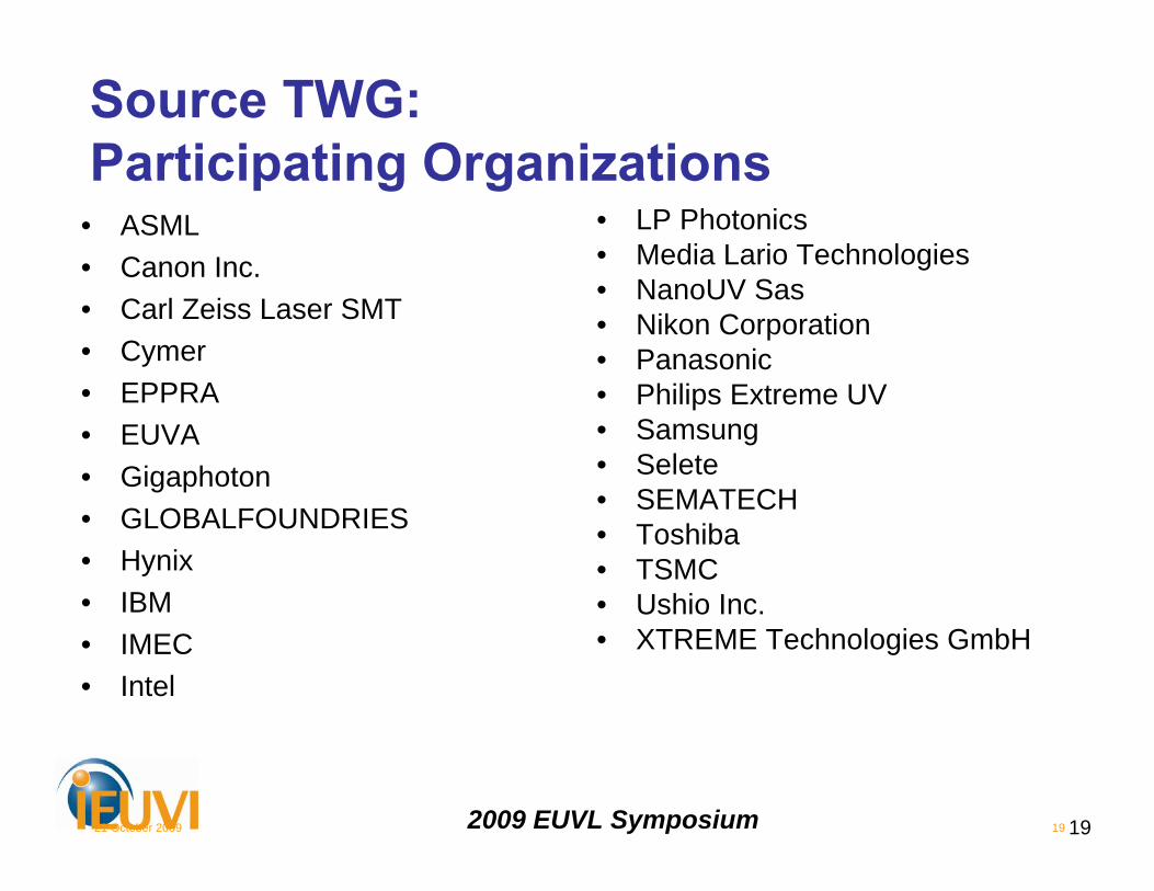
Source TWG:Participating Organizations
• ASML• Canon Inc.• Carl Zeiss Laser SMT• Cymer• EPPRA• EUVA• Gigaphoton• GLOBALFOUNDRIES• Hynix• IBM• IMEC• Intel
• LP Photonics• Media Lario Technologies• NanoUV Sas• Nikon Corporation• Panasonic• Philips Extreme UV• Samsung• Selete• SEMATECH• Toshiba• TSMC• Ushio Inc.• XTREME Technologies GmbH

202009 EUVL Symposium
Source TWG: Accomplishments• Drive standards development
– Development of specifications for collector lifetime requirements for alpha, beta and gamma level EUV sources
– Development of standards for Intermediate Focus (IF) metrology– Identified interface opportunities for the industry to reduce
cumulative development costs• Drive industry consensus on critical technical
challenges for EUV source commercialization– Identify and rank critical issues for EUV source technology– Map which of the stake holders will be addressing which EUV source
critical issue and which issues are not being addressed– Consolidated supplier source performance data into a summary table

212009 EUVL Symposium21 October 2009 21
2009 On Line Survey Results (89 replies) Leading EUV Source Technology?
Pilot line HVM
LPP65%
DPP32%
LPP55%
DPP44%

222009 EUVL Symposium21 October 2009 22
Survey ResultsHVM DPP SoCoMo: Showstopper ?
Yes
DPP

232009 EUVL Symposium21 October 2009 23
Survey ResultsHVM LPP SoCoMo: Showstopper ?
Yes
LPP

242009 EUVL Symposium
EUV Sources for Actinic Metrology
• Several potential source technologies are being considered for actinic EUV mask metrology inspection tools.
• These source technologies are currently at the development stage and require funding to develop the first generation of fully integrated sources that meet the power and brightness requirements for actinic mask metrology.
• Lack of funding could jeopardize the insertion of EUV lithography at the 22 nm half-pitch node by 2013.
21 October 2009 24

252009 EUVL Symposium
Outline• Background and ITRS Lithography• IEUVI Overview• Source TWG• Resist TWG• Mask TWG• EUV Mask Infrastructure Development• Summary

262009 EUVL Symposium
Resist TWG: Participating Organizations
• AIXUV • ASML • ASET • BOC Edwards• Brewer Science • Canon• Ceil Indus. • CEA/LETI • Dongjin • Energetiq • Fujifilm• Global Foundry• Honeywell • IBM • IMEC • Intel • JSR
• Nikon• Nissan Chem.• Osaka University • Philips• Panasonic • Rohm & Haas (Dow) • Samsung • SELETE • SEMATECH • Shin-Etsu • Sumitomo • SUNY Albany • Texas Instruments • TOK• University of Birmingham • University of Hyogo• University of Illinois

272009 EUVL Symposium
Resist TWG: Mission & Objective• Mission: Increased cooperation among EUV resist development
community world wide– Coordinate efforts to identify & address top issues
• Objective: Provide forum to share information to foster global collaboration to accelerate development of EUV resists
Sept. 2008LBNL e-MET
15mJ 24nm hp
22nm hp
20nm hp
1.05
1.00
0.95
0.90
0.85
0.80
24nm hp Focus (um
)
14mJ
Sept. 2009Albany e-MET
Resolution: 22-24nm hpLWR: 4.8nmSensitivity: 14mJ/cmDOF: 250nm @ 24nm hp

282009 EUVL Symposium
28nm 26nm 24nm30nm 22nm 20nm
UL/Resist: UL-1(20nm) / STM-3 (40nm)PAB: 110C/90secPEB: 100C/60secDev: 2.38% TMAH / 30secExp: Albany E-MET 0.3NA Quad
UL-1/SMT-316.8 mJ/cm2
HMDS Si/STM-220.0 mJ/cm2
Resolution using Quadrupole Illumination with three different suppliers CAR resists
UL/Resist: Si HMDS / STM-2 (50nm)PAB: 110C/90secPEB: 100C/90secDev: 2.38% TMAH / 30secExp: Albany E-MET 0.3NA Quad
UL/Resist: UL-1(20nm) / STM-5 (50nm)PAB: 110C/60secPEB: 100C/60secDev: 2.38% TMAH / 30secExp: Albany E-MET 0.3NA Quad
UL-1/SMT-514.0 mJ/cm2

292009 EUVL Symposium
ADT Resolution to 26nm hp Demonstrated
*C. Koh et. al.EUVL 09 Poster
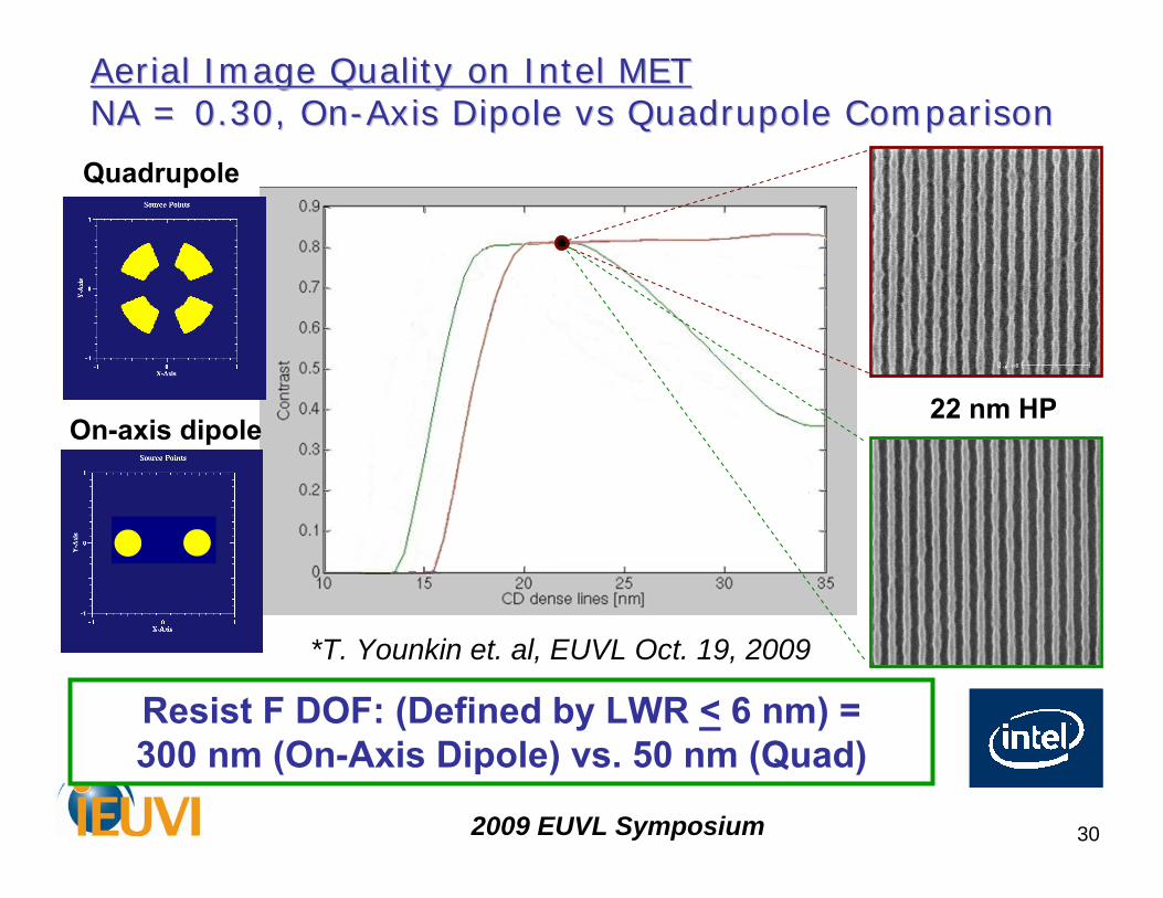
302009 EUVL Symposium
*T. Younkin et. alEUVL Oct. 18
Quadrupole
Resist F DOF: (Defined by LWR < 6 nm) = 300 nm (On-Axis Dipole) vs. 50 nm (Quad)
22 nm HPOn-axis dipole
Aerial Image Quality on Intel METAerial Image Quality on Intel METNA = 0.30, OnNA = 0.30, On--Axis Dipole vs Quadrupole ComparisonAxis Dipole vs Quadrupole Comparison
*T. Younkin et. al, EUVL Oct. 19, 2009
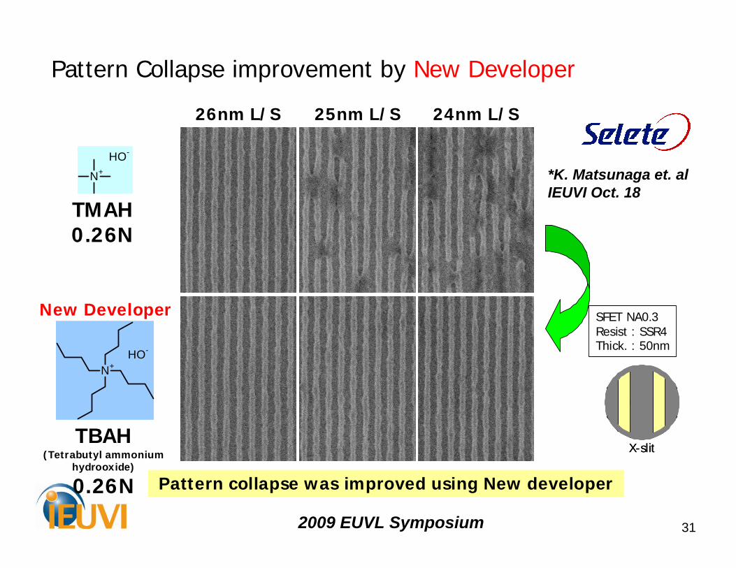
312009 EUVL Symposium
Pattern Collapse improvement by New Developer
26nm L/S 25nm L/S 24nm L/S
TMAH0.26N
New Developer SFET NA0.3Resist : SSR4Thick. : 50nm
X-slitX-slit
Pattern collapse was improved using New developer
N+HO-
N+
HO-
TBAH(Tetrabutyl ammonium
hydrooxide)
0.26N
*K. Matsunaga et. alIEUVI Oct. 18

322009 EUVL Symposium
Resist TWG 22nm hp Status UpdateProgress• Several resist vendors are now demonstrating 24-22nm hp resolution with CAR
on all EUV Micro Exposure Tools– Good 24nm hp process windows at 50nm resist thickness have been demonstrated
on METs– Under-Layer/Resist stack optimization improving process windows and helping LWR– Resist sensitivity improving with several ~10mJ/cm2 resists with good resolution
(26nm hp demonstrated)– SEMATECH relaxed resist outgassing Spec to 3x10¹⁵ for ADT, is now allowing best in
class resist screening on full field tool– New resist platforms (Molecular glass) continue to improve but CAR resists continue to
be best in overall RLS performance
Current Gaps– Pattern collapse reduction work needed for 24nm hp and below– LWR in resist only down to ~4.5nm at 24nm hp– Post litho process combined with optimized pattern transfer work required to drive
LWR below 2nm– Understanding how MET imaging performance translates to full field tools is needed– Higher NA & Sigma METs needed to push beyond 20nm hp – 4-5x Masks with sub 22nm hp resolution needed for sub 22nm materials development

332009 EUVL Symposium
Reducing LWR Gap with Post Processing?
Grazing incidence Ion Beam2
•LWR reduced from 9.7-5.5nm @ 40nm hp•Less than 10% resist CD/Thickness change •30-40% reduction @ 300 wafer/hr
Pattern transfer Optimization3
•LWR reduced from 9.7-> 4.0nm in HM transfer•LWR reduced further 4.7-> ~2.2nm at 32nm•Greater than 10% CD change/trim•20-40% reduction with standard HM pattern transfer
Post develop Rinse1
•LWR reduced from 5.3-3.9nm @ 30nm hp•Little to no resist CD change•25% reduction no throughput impact
1) G. Vandentop, et al 2009 SPIE Keynote2) David Ruzic et al. Proc SPIE Vol. 7273, 727346, 20093) Lam Research LWR proposal to SEMATECH RFI
Can various post processing methods combined
with pattern transfer reduce LWRby 60-70% in final device features?

342009 EUVL Symposium
Next IEUVI Resist TWG MeetingFeb. 2010 @ SPIE

352009 EUVL Symposium
Outline• Background and ITRS Lithography• IEUVI Overview• Source TWG• Resist TWG• Mask TWG• EUV Mask Infrastructure Development• Summary

362009 EUVL Symposium
Mask TWG: Mission & Objective• Mission:
Ensure EUV Mask Infrastructure Readiness for:• Pilot Line Production 2010 – 2012• High Volume Manufacturing 2013 - 2016
• Objectives:– Identify Required Standards– Coordinate industry-wide conversions, such as
future mask incidence angle change.– Identify any gaps between current industry
efforts and projected future needs– Highlight gaps to member organizations and
IEUVI Board for action

372009 EUVL Symposium
Mask TWG: Members• Alcatel• AMD• AMTC • Asahi Glass Co. • ASML • Canon• Carl Zeiss• CSNE• Corning Inc. • Dai Nippon Printing• Entegris• Hanyang University• Hoya Corp.• IBM • Intel• IMEC• KLA-Tencor
• Lasertec• Lawrence Berkeley N.L. • Nikon• NuFlare Technology Inc.• Ohara• Photronics• Qimonda • Samsung • SELETE • SEMATECH • SEMI• Toppan Printing Co.• Toshiba• TOSO• TSMC• Veeco Instruments Inc.• Wisconsin University• UMC

382009 EUVL Symposium
Mask TWG: 2009 Accomplishment• SEMI Standard Accomplishment
– E152 - Mechanical Specification of EUV Pod for 150 mm EUVL Reticles• Adjudicated in April 2009, published in July 2009
– P40 - Mounting Requirements for EUV Masks• Adjudicated on July 14, 2009, will be published this year
– P37 – Specification for Extreme Ultraviolet Lithography Substrates and Blanks
• Adjudicated in September, 2009, will be published this year– Specification of Fiducial Marks for EUV Mask Blanks
• Agreement made by taskforce to submit blue ballot in Q4, ‘09; yellow in Q1, ‘10• Dual Pod Status
– SEMI compliant Dual Pods arrived in SEMATECH in June– Particle protection testing is on-going
• ITRS EUV Mask Specifics– Team formed. Survey results rolled up.– 7 parameters with agreed changes. Six areas identified champions for next
revision.

392009 EUVL Symposium
Mask TWG: Development Gaps (to be discussed at Thursday TWG)
Pilot Line 2010-2012:– Substrate: Polish defects, flatness, defect inspection & analysis– Blanks: ML deposition, reflectivity uniformity, defect inspection
& analysis & repair– Mask Writing: Pattern defect inspection, full-field actinic
inspection, – Pattern Repair: FIB Tool/process, small-field actinic inspection– Fab use: In-Fab inspection and cleans
HVM issues (> 2013)– When does mask incidence angle change from 6º to ≥ 8º ?– Mask defect printability and fiducial mark implementation

402009 EUVL Symposium
Challenges• Mask defect reduction during mask make
– Industrial consensus of inspection and defect review strategy and affordable path of implementation
– Printability study• Size, Depth, Shape, Pattern• Defect printability mask availability and standardization
– Blank defect inspection and reduction– ML defect inspection and reduction– Mask writing defect inspection and repair– Fiducial mark implementation – Mask surface roughness on resist LER and inspection
sensitivity• Mask quality control during mask use
– Dual Pod compatible interface– Mask storage (defects and potential progressive growth
prevention) – Cleaning

412009 EUVL Symposium
Plans• Short Term (Pilot Line 2010-2012)
– Refine/Update ITRS roadmap– Update/Establish SEMI standards– Address and take steps to close key mask
infrastructure gaps (e.g. inspection) towards pilot line and HVM needs
• Long Term (HVM > 2013)– Mask defect reduction– Mask life time improvement

422009 EUVL Symposium
Outline• Background and ITRS Lithography• IEUVI Overview• Source TWG• Resist TWG• Mask TWG• EUV Mask Infrastructure Development• Summary

432009 EUVL Symposium
SEMATECH EUV Mask Infrastructure Technical and Business Working Groups*• In July, SEMATECH conducted a Workshop on EUV Mask
Infrastructure– Attended by executives from over 20 EUV stakeholders including
chip, mask, blank and tool makers– Consensus output from meeting was
• Actinic tools will not be in time for 2011 Pilot Line• Existing mask metrology capability must be understood and extended to
support through pilot line• HVM requirements must be specified and new tool needs identified• Funding for new tools must be obtained and pooled in a new consortium
• SEMATECH is leading the formation if this new mask infrastructure consortium– Formed Technical Working to specify requirements and gaps– Formed Business Working group to create workable funding models
*See Brian Rice’s presentation: Reticle Inspection Gap

442009 EUVL Symposium
SEMATECH EUV Mask Infrastructure (EMI) Consortium
TechnicalWorking Group
BusinessWorking Group
ConsortiumFunding ($200M+)
Actinic EUV Mask Inspection Tools
• SEMATECH technical working group (EMI TWG)– Customers, suppliers, SEMATECH facilitation– Establish consensus on requirements (need, tool types, timing, initial
specifications, ..)
• SEMATECH business working group (EMI BWG)– Suppliers, customers, consortia, funders– Consortia member LOI funding commitments by year end
452009 EUVL Symposium
SEMATECH Consortium Output• The Technical Working Group has assessed the capability
of a large number of metrology tools and has concluded pilot line needs can be met without actinic equipment:– Existing substrate and blank inspection capability exits down to
~40nm sensitivity and can likely to upgraded to 25nm sensitivity– Print testing can satisfy AIMS need in the short term– Optical patterned mask inspection can support 22nm pilot line– Actinic blank inspection and AIMS are critical for 22nm HVM– Advanced PMI is needed beyond 22nm (actinic/ebeam/etc)
• The Business Working Group has identified consensus funding models– Those who benefit from EUV pay mask metro NRE
• Need $250M+ NRE to fund all three tools– NRE is recovered through royalties on tool sales and blank sales– Needed actinic tools would start becoming available in 2013

462009 EUVL Symposium
Outline• Background and ITRS Lithography• IEUVI Overview• Source TWG• Resist TWG• Mask TWG• EUV Mask Infrastructure Development• Summary
472009 EUVL Symposium
Summary• Good progress overall! Attention is shifting on cost of
ownership, items missing in infrastructure and realistic insertion schedule (i.e., Pilot Line, HVM)
• Cooperation is even more relevant than ever before as EUV infrastructure development remains a major risk for EUV insertion ( i.e., contact the IEUVI TWG Chairs if you have contributions!) http://www.ieuvi.org
• Sematech Mask Infrastructure Business Working Group (EMI BWG) proposed!
• Do additional BWGs need to be formed to address commercialization of EUV?
• There are not too many technology nodes left for EUV to make a difference!


![Botany 0910 Info]](https://static.fdocuments.us/doc/165x107/54180e917bef0a05088b4572/botany-0910-info.jpg)