0.9 1nch 2 Digit
14
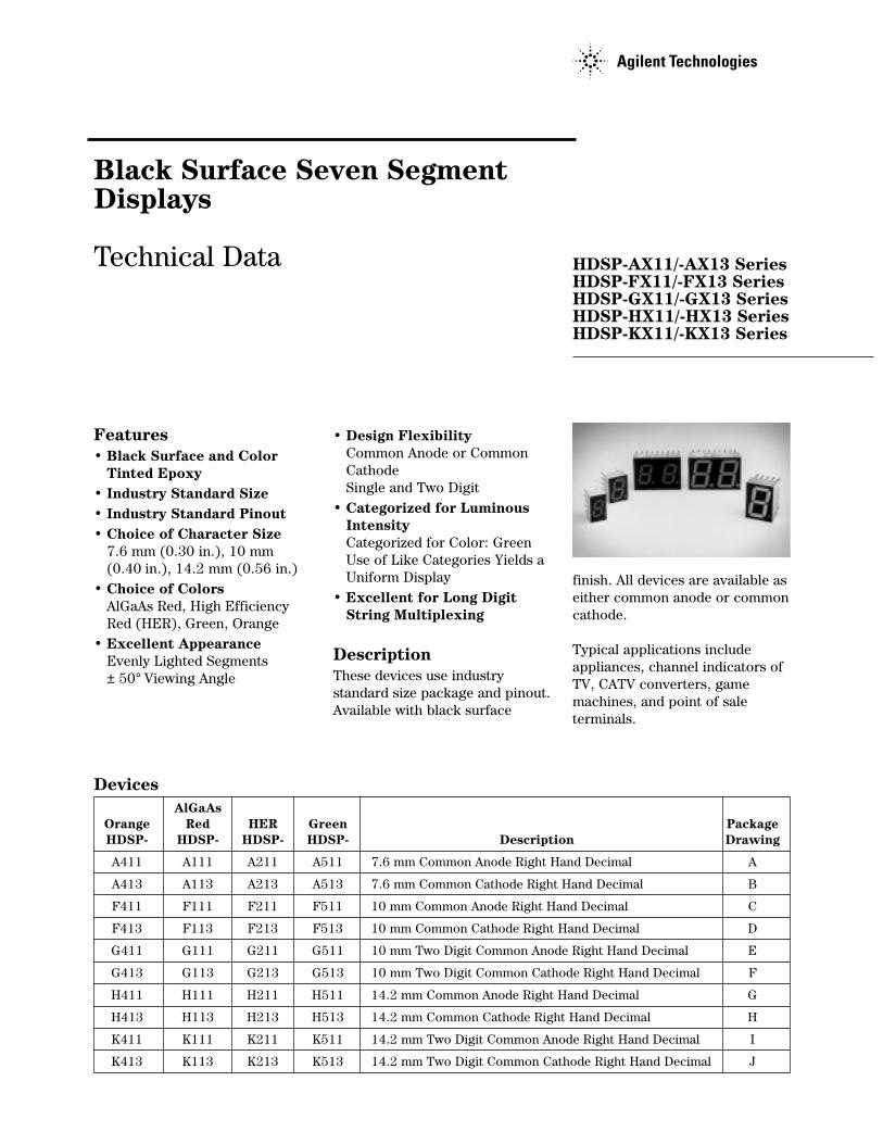
Devices AlGaAs Orange Red HER Green Package HDSP- HDSP- HDSP- HDSP- Description Drawing A411 A111 A211 A511 7.6 mm Common Anode Right Hand Decimal A A413 A113 A213 A513 7.6 mm Common Cathode Right Hand Decimal B F411 F111 F211 F511 10 mm Common Anode Right Hand Decimal C F413 F113 F213 F513 10 mm Common Cathode Right Hand Decimal D G411 G111 G211 G511 10 mm Two Digit Common Anode Right Hand Decimal E G413 G113 G213 G513 10 mm Two Digit Common Cathode Right Hand Decimal F H411 H111 H211 H511 14.2 mm Common Anode Right Hand Decimal G H413 H113 H213 H513 14.2 mm Common Cathode Right Hand Decimal H K411 K111 K211 K511 14.2 mm Two Digit Common Anode Right Hand Decimal I K413 K113 K213 K513 14.2 mm Two Digit Common Cathode Right Hand Decimal J Black Surface Seven Segment Displays Technical Data Features • Black Surface and Color Tinted Epoxy • Industry Standard Size • Industry Standard Pinout • Choice of Character Size 7.6 mm (0.30 in.), 10 mm (0.40 in.), 14.2 mm (0.56 in.) • Choice of Colors AlGaAs Red, High Efficiency Red (HER), Green, Orange • Excellent Appearance Evenly Lighted Segments ± 50° Viewing Angle • Design Flexibility Common Anode or Common Cathode Single and Two Digit • Categorized for Luminous Intensity Categorized for Color: Green Use of Like Categories Yields a Uniform Display • Excellent for Long Digit String Multiplexing Description These devices use industry standard size package and pinout. Available with black surface HDSP-AX11/-AX13 Series HDSP-FX11/-FX13 Series HDSP-GX11/-GX13 Series HDSP-HX11/-HX13 Series HDSP-KX11/-KX13 Series finish. All devices are available as either common anode or common cathode. Typical applications include appliances, channel indicators of TV, CATV converters, game machines, and point of sale terminals.
Transcript of 0.9 1nch 2 Digit
DevicesAlGaAs
Orange Red HER Green PackageHDSP- HDSP- HDSP- HDSP- Description Drawing
A411 A111 A211 A511 7.6 mm Common Anode Right Hand Decimal A
A413 A113 A213 A513 7.6 mm Common Cathode Right Hand Decimal B
F411 F111 F211 F511 10 mm Common Anode Right Hand Decimal C
F413 F113 F213 F513 10 mm Common Cathode Right Hand Decimal D
G411 G111 G211 G511 10 mm Two Digit Common Anode Right Hand Decimal E
G413 G113 G213 G513 10 mm Two Digit Common Cathode Right Hand Decimal F
H411 H111 H211 H511 14.2 mm Common Anode Right Hand Decimal G
H413 H113 H213 H513 14.2 mm Common Cathode Right Hand Decimal H
K411 K111 K211 K511 14.2 mm Two Digit Common Anode Right Hand Decimal I
K413 K113 K213 K513 14.2 mm Two Digit Common Cathode Right Hand Decimal J
Black Surface Seven SegmentDisplays
Technical Data
Features• Black Surface and Color
Tinted Epoxy• Industry Standard Size• Industry Standard Pinout• Choice of Character Size
7.6 mm (0.30 in.), 10 mm(0.40 in.), 14.2 mm (0.56 in.)
• Choice of ColorsAlGaAs Red, High EfficiencyRed (HER), Green, Orange
• Excellent AppearanceEvenly Lighted Segments± 50° Viewing Angle
• Design FlexibilityCommon Anode or CommonCathodeSingle and Two Digit
• Categorized for LuminousIntensityCategorized for Color: GreenUse of Like Categories Yields aUniform Display
• Excellent for Long DigitString Multiplexing
DescriptionThese devices use industrystandard size package and pinout.Available with black surface
HDSP-AX11/-AX13 SeriesHDSP-FX11/-FX13 SeriesHDSP-GX11/-GX13 SeriesHDSP-HX11/-HX13 SeriesHDSP-KX11/-KX13 Series
finish. All devices are available aseither common anode or commoncathode.
Typical applications includeappliances, channel indicators ofTV, CATV converters, gamemachines, and point of saleterminals.

2
Part Numbering System
Notes:1. For codes not listed in the figure above, please refer to the respective datasheet or contact your nearest
Agilent representative for details.2. Bin options refer to shippable bins for a part number. Color and Intensity Bins are typically restricted to 1
bin per tube (exceptions may apply). Please refer to respective datasheet for specific bin limit information.
5082 -X X X X-X X X X XHDSP-X X X X-X X X X X
Mechanical Options[1]
00: No Mechanical Option
Color Bin Options[1,2]
0: No Color Bin Limitation
Maximum Intensity Bin[1,2]
0: No Maximum Intensity Bin Limitation
Minimum Intensity Bin[1,2]
0: No Minimum Intensity Bin Limitation
Device Configuration/Color[1]
1: Common Anode3: Common Cathode
Device Specific Configuration[1]
Refer to Respective Datasheet
Package[1]
A: 7.6 mm (0.3 inch) Single Digit Seven Segment DisplayF: 10 mm (0.4 inch) Single Digit Seven Segment DisplayG: 10 mm (0.4 inch) Dual Digit Seven Segment DisplayH: 14.2 mm (0.56 inch) Single Digit Seven Segment DisplayK: 14.2 mm (0.56 inch) Dual Digit Seven Segment Display

3
Package Dimensions (7.6 mm Series) Internal Circuit Diagram
Package Dimensions (10 mm Series: Single) Internal Circuit Diagram
4
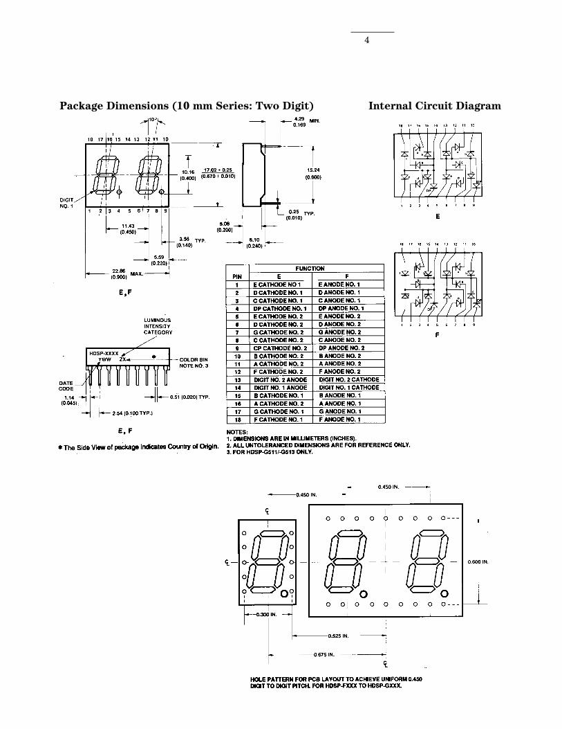
Package Dimensions (10 mm Series: Two Digit) Internal Circuit Diagram
5
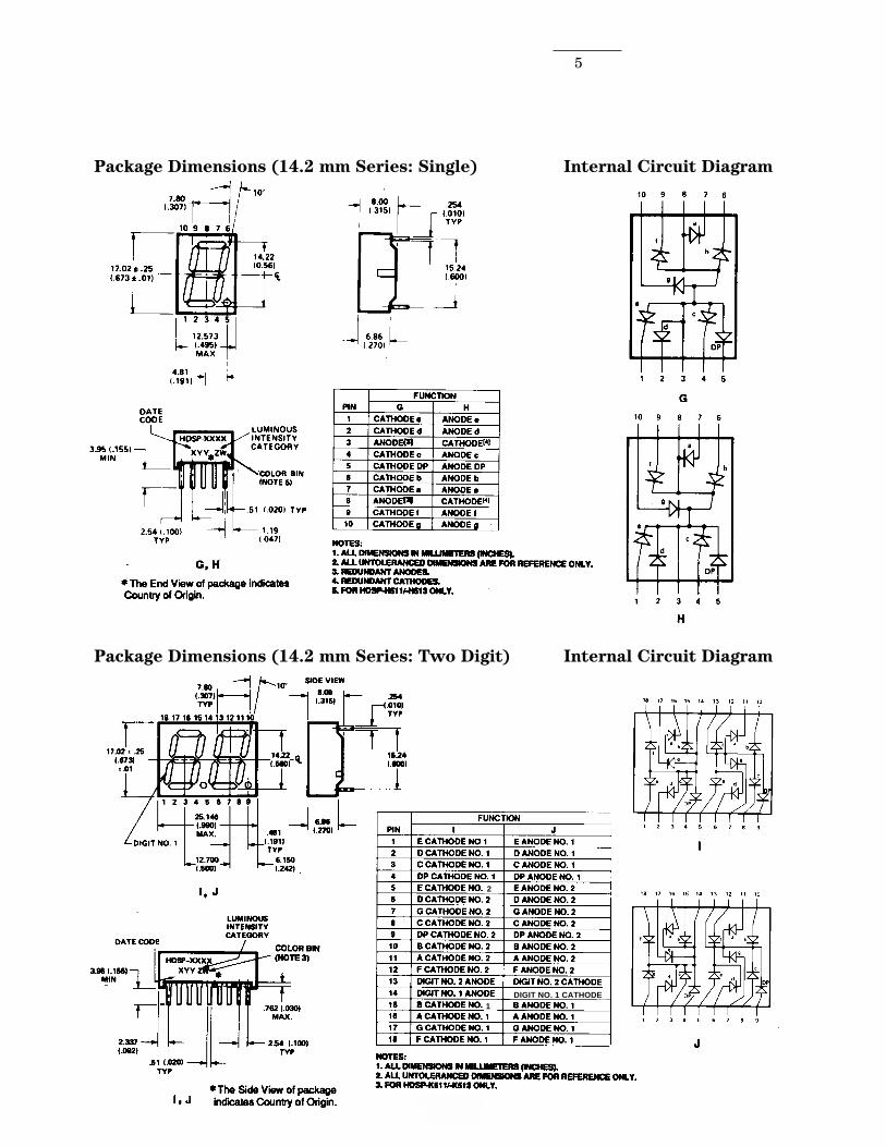
Package Dimensions (14.2 mm Series: Single) Internal Circuit Diagram
Package Dimensions (14.2 mm Series: Two Digit) Internal Circuit Diagram
2
1DIGIT NO. 1 CATHODE
6
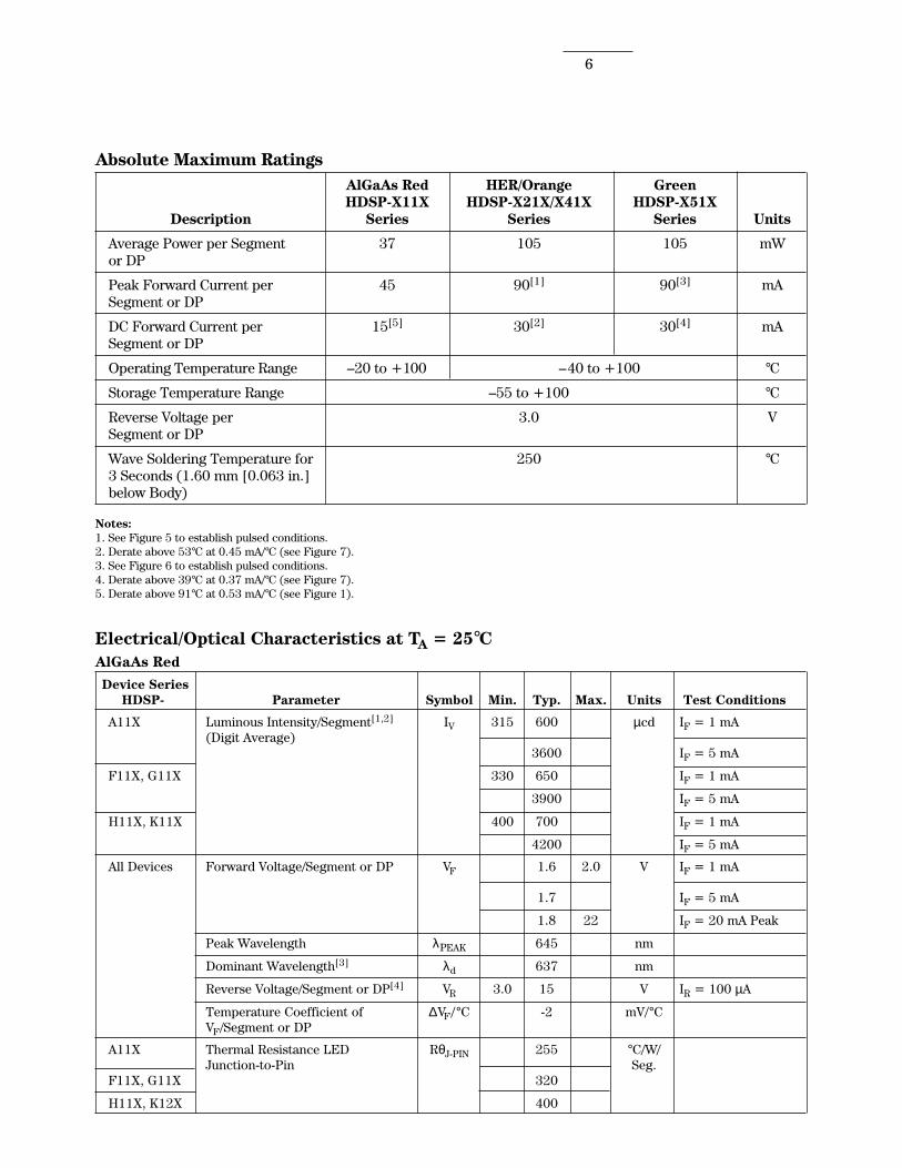
AlGaAs Red
Device SeriesHDSP- Parameter Symbol Min. Typ. Max. Units Test Conditions
A11X Luminous Intensity/Segment[1,2] IV 315 600 µcd IF = 1 mA(Digit Average)
3600 IF = 5 mA
F11X, G11X 330 650 IF = 1 mA
3900 IF = 5 mA
H11X, K11X 400 700 IF = 1 mA
4200 IF = 5 mA
All Devices Forward Voltage/Segment or DP VF 1.6 2.0 V IF = 1 mA
1.7 IF = 5 mA
1.8 22 IF = 20 mA Peak
Peak Wavelength λPEAK 645 nm
Dominant Wavelength[3] λd 637 nm
Reverse Voltage/Segment or DP[4] VR 3.0 15 V IR = 100 µA
Temperature Coefficient of ∆VF/°C -2 mV/°CVF/Segment or DP
A11X Thermal Resistance LED RθJ-PIN 255 °C/W/Junction-to-Pin Seg.
F11X, G11X 320
H11X, K12X 400
Electrical/Optical Characteristics at TA = 25°C
Absolute Maximum RatingsAlGaAs Red HER/Orange GreenHDSP-X11X HDSP-X21X/X41X HDSP-X51X
Description Series Series Series Units
Average Power per Segment 37 105 105 mWor DP
Peak Forward Current per 45 90[1] 90[3] mASegment or DP
DC Forward Current per 15[5] 30[2] 30[4] mASegment or DP
Operating Temperature Range –20 to +100 –40 to +100 °C
Storage Temperature Range –55 to +100 °C
Reverse Voltage per 3.0 VSegment or DP
Wave Soldering Temperature for 250 °C3 Seconds (1.60 mm [0.063 in.]below Body)
Notes:1. See Figure 5 to establish pulsed conditions.2. Derate above 53°C at 0.45 mA/°C (see Figure 7).3. See Figure 6 to establish pulsed conditions.4. Derate above 39°C at 0.37 mA/°C (see Figure 7).5. Derate above 91°C at 0.53 mA/°C (see Figure 1).

7
High Efficiency Red
Device SeriesHDSP- Parameter Symbol Min. Typ. Max. Units Test Conditions
A21X Luminous Intensity/Segment[1,2] IV 360 980 µcd IF = 5 mA(Digit Average)
5390 IF = 20 mA
F21X, G21X 420 1200 IF = 5 mA
H21X, K21X 900 2800 IF = 10 mA
3700 IF = 60 mA Peak:1/6 Duty Factor
All Forward Voltage/Segment or DP VF 2.0 2.5 V IF = 20 mADevices
Peak Wavelength λPEAK 635 nm
Dominant Wavelength[3] λd 626 nm
Reverse Voltage/Segment or DP[4] VR 3.0 30 V IR = 100 µA
Temperature Coefficient of ∆VF/°C -2 mV/°CVF/Segment or DP
A21X Thermal Resistance LED RθJ-PIN 200 °C/W/Junction-to-Pin Seg.
F21X, G21X 320
H21X, K21X 345
Orange
Device SeriesHDSP- Parameter Symbol Min. Typ. Max. Units Test Conditions
A41X Luminous Intensity/Segment IV 0.70 mcd IF = 5 mA(Segment Average)[1,2]
F41X, G41X 1.0 IF = 5 mA
H41X, K41X 2.37 IF = 10 mA
All Forward Voltage/Segment or DP VF 2.0 2.5 V IF = 20 mADevices
Peak Wavelength λPEAK 600 nm
Dominant Wavelength[3] λd 603 nm
Reverse Voltage/Segment or DP[4] VR 3.0 30 V IR = 100 µA
Temperature Coefficient of ∆VF/°C –2 mV/°CVF/Segment or DP
A41X Thermal Resistance LED RθJ-PIN 200 °C/W/Junction-to-Pin Seg.
F41X, G41X 320
H41X, K41X 345
8
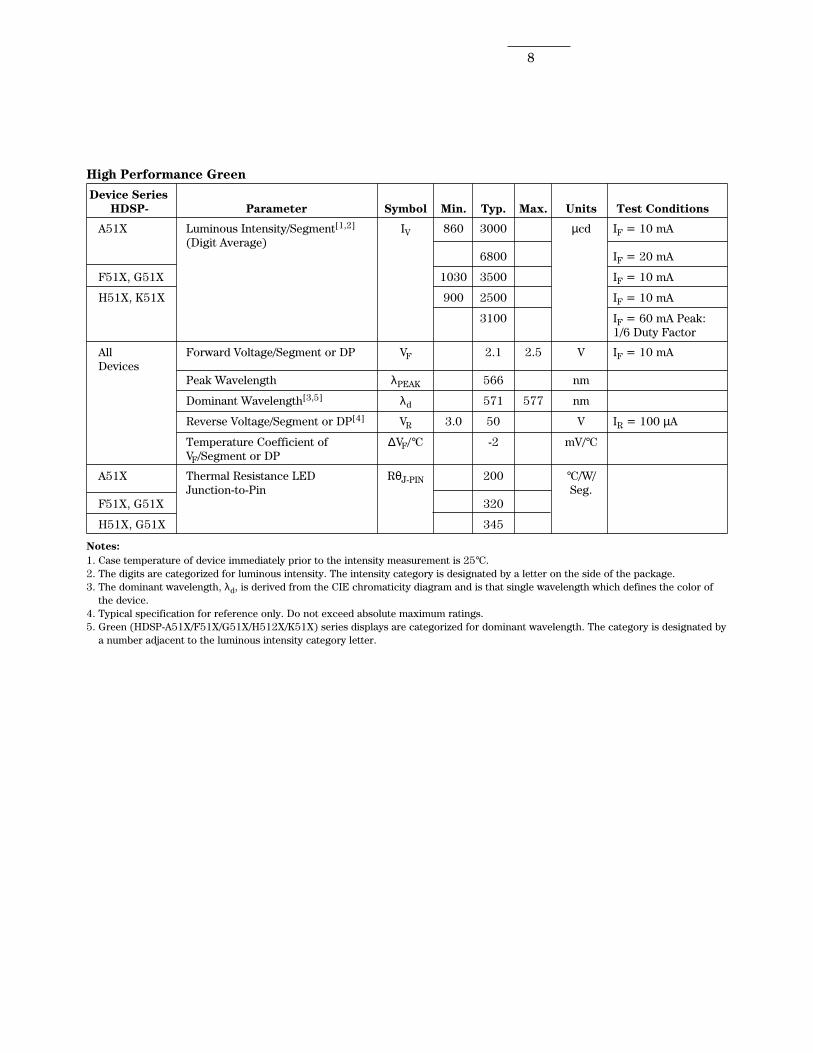
High Performance Green
Device SeriesHDSP- Parameter Symbol Min. Typ. Max. Units Test Conditions
A51X Luminous Intensity/Segment[1,2] IV 860 3000 µcd IF = 10 mA(Digit Average)
6800 IF = 20 mA
F51X, G51X 1030 3500 IF = 10 mA
H51X, K51X 900 2500 IF = 10 mA
3100 IF = 60 mA Peak:1/6 Duty Factor
All Forward Voltage/Segment or DP VF 2.1 2.5 V IF = 10 mADevices
Peak Wavelength λPEAK 566 nm
Dominant Wavelength[3,5] λd 571 577 nm
Reverse Voltage/Segment or DP[4] VR 3.0 50 V IR = 100 µA
Temperature Coefficient of ∆VF/°C -2 mV/°CVF/Segment or DP
A51X Thermal Resistance LED RθJ-PIN 200 °C/W/Junction-to-Pin Seg.
F51X, G51X 320
H51X, G51X 345
Notes:1. Case temperature of device immediately prior to the intensity measurement is 25°C.2. The digits are categorized for luminous intensity. The intensity category is designated by a letter on the side of the package.3. The dominant wavelength, λd, is derived from the CIE chromaticity diagram and is that single wavelength which defines the color of
the device.4. Typical specification for reference only. Do not exceed absolute maximum ratings.5. Green (HDSP-A51X/F51X/G51X/H512X/K51X) series displays are categorized for dominant wavelength. The category is designated by
a number adjacent to the luminous intensity category letter.

9
Figure 3. Relative Luminous Intensityvs. DC Forward Current.
Figure 4. Relative Efficiency (LuminousIntensity per Unit Current) vs. Peak Current.
Figure 1. Maximum Allowable Average orDC Current vs. Ambient Temperature.
Figure 2. Forward Current vs. Forward Voltage.
16
0
2
4
6
8
10
12
14
20 10090807060504030
T – AMBIENT TEMPERATURE – °CA
I A
VE
. MA
X –
MA
XIM
UM
AV
ER
AG
EF
OR
WA
RD
CU
RR
EN
T P
ER
SE
GM
EN
T –
mA
F
120110
20
18R = 770°C/WθθθθJ-A
F
50.0
20.0
10.0
5.0
2.0
1.0
0.5
0.1
0 0.5 1.0 1.5 2.0 2.5
V – FORWARD VOLTAGE – VF
I –
FO
RW
AR
D C
UR
RE
NT
PE
R S
EG
ME
NT
– m
A20
10
5
2
1
0.5
0.2
0.10.1 0.2 0.5 1 2 5 10 20
RE
LA
TIV
E L
UM
INO
US
INT
EN
SIT
Y
(NO
RM
AL
IZE
D T
O 1
AT
1 m
A)
I – FORWARD CURRENTPER SEGMENT – mA
F I – PEAK FORWARD CURRENTPER SEGMENT – mA
PEAK
ηηηη
–
RE
LA
TIV
E E
FF
ICIE
NC
Y –
N
OR
MA
LIZ
ED
TO
1 A
T 1
mA
PE
AK
1.3
1.2
1.1
1.0
0.9
0.8
0 5 10 20 30 40 500.7
0.5 mA
AlGaAs Red

10
HER, Green, Orange
Figure 7. Maximum Allowable DCCurrent vs. Ambient Temperature.
Figure 8. Forward Current vs.Forward Voltage Characteristics.
Figure 9. Relative Luminous Intensityvs. DC Forward Current.
Figure 10. Relative Efficiency (Luminous Intensityper Unit Current) vs. Peak Current.
40
0
5
10
15
20
25
30
35
20 10090807060504030
T – AMBIENT TEMPERATURE – °CA
I
MA
X –
MA
XIM
UM
DC
CU
RR
EN
T
PE
R S
EG
ME
NT
– m
AD
C
120110
50
45
HER / ORANGEGREEN
R = 770°C/Wθ J-A
0
100
80
60
40
20
I –
FO
RW
AR
D C
UR
RE
NT
PE
R S
EG
ME
NT
– m
AF
2.0 4.03.01.0
V – FORWARD VOLTAGE – VF
0 5.0
HER / ORANGE
GREEN
η PE
AK
– R
EL
AT
IVE
LU
MIN
OU
S IN
TE
NS
ITY
(NO
RM
AL
IZE
D T
O 1
AT
5 m
A F
OR
HE
R,
AN
D T
O 1
AT
10
mA
FO
R G
RE
EN
)
150
10
8
6
4
2
205 3010 25
12
I – FORWARD CURRENT PER SEGMENT – mAF
0
GREEN
HER / ORANGE
0
I – PEAK FORWARD CURRENT PER SEGMENT – mA
PEAK
0.8
1.0
1.2
1.4
10020 806040
1.8
1.6
GREEN
HER / ORANGE
η PE
AK
– R
EL
AT
IVE
EF
FIC
IEN
CY
(NO
RM
AL
IZE
D T
O 1
AT
5 m
A F
OR
HE
R,
AN
D 1
0 m
A F
OR
GR
EE
N)
Figure 5. Maximum Tolerable Peak Currentvs. Pulse Duration – HER, Orange.
Figure 6. Maximum Tolerable PeakCurrent vs. Pulse Duration – Green.
RA
TIO
OF
MA
XIM
UM
OP
ER
AT
ING
PE
AK
CU
RR
EN
T T
O T
EM
PE
RA
TU
RE
D
ER
AT
ED
DC
CU
RR
EN
T
I P
EA
KF
I
MA
XD
C
t – PULSE DURATION – µsP
10
1
100
10 1000010001001
10 KH
z3 K
Hz
300 Hz
DC OPERATION
OPERATION IN THISREGION REQUIRESTEMPERATUREDERATING OF IMAXIMUM
DC
100 Hz
1 KH
z
RA
TIO
OF
MA
XIM
UM
OP
ER
AT
ING
PE
AK
CU
RR
EN
T T
O T
EM
PE
RA
TU
RE
D
ER
AT
ED
DC
CU
RR
EN
T
I P
EA
KF
I
MA
XD
C
t – PULSE DURATION – µsP
10
1
100
10 1000010001001
10 KH
z
3 KH
z
300 Hz
100 HzDC OPERATION
OPERATION IN THISREGION REQUIRESTEMPERATUREDERATING OF IMAXIMUM
DC
1 Hz

11
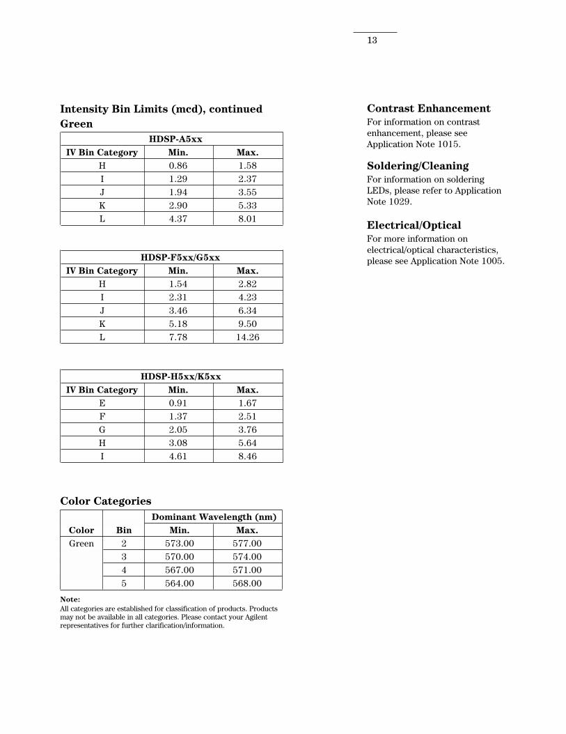
HDSP-A1xx IV Bin Category Min. Max.
E 0.315 0.520F 0.428 0.759G 0.621 1.16H 0.945 1.71I 1.40 2.56J 2.10 3.84K 3.14 5.75L 4.70 8.55
Intensity Bin Limits (mcd)AlGaAs Red
HDSP-F1xx/G1xx IV Bin Category Min. Max.
D 0.391 0.650E 0.532 0.923F 0.755 1.39G 1.13 2.08H 1.70 3.14
HDSP-H1xx/K1xx IV Bin Category Min. Max.
C 0.415 0.690D 0.565 0.990E 0.810 1.50F 1.20 2.20G 1.80 3.30H 2.73 5.00I 4.09 7.50
OrangeHDSP-A41X
IV Bin Category Min MaxA 0.284 0.433B 0.354 0.541C 0.443 0.677D 0.554 0.846E 0.692 1.057F 0.856 1.322G 1.082 1.652H 1.352 2.066I 1.692 2.581J 2.114 3.227K 2.641 4.034L 3.300 5.042M 4.127 6.303N 5.157 7.878
HDSP-F41X/G41XIV Bin Category Min Max
C 0.485 0.890D 0.728 1.333E 1.091 2.000F 1.636 3.000G 2.454 4.500H 3.682 6.751
HDSP-H41X/K41XIV Bin Category Min Max
B 0.77 1.17C 0.95 1.45D 1.19 1.82E 1.49 2.27F 1.85 2.89G 2.32 3.54H 2.90 4.43
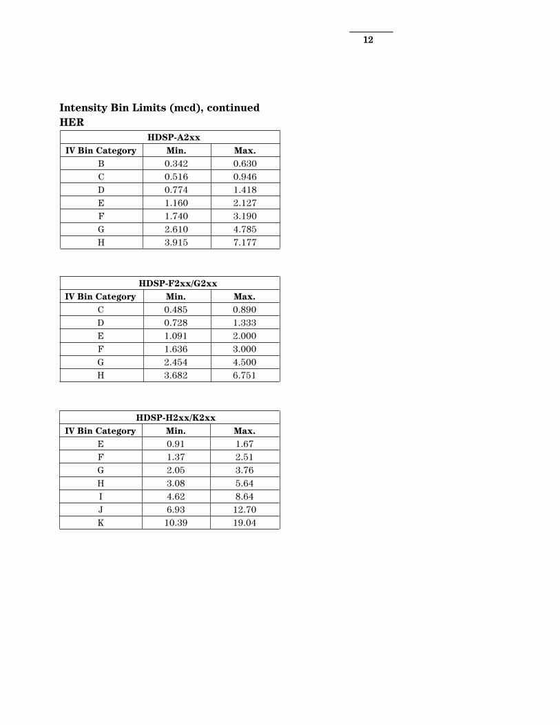
12
HDSP-A2xx IV Bin Category Min. Max.
B 0.342 0.630C 0.516 0.946D 0.774 1.418E 1.160 2.127F 1.740 3.190G 2.610 4.785H 3.915 7.177
HDSP-F2xx/G2xx IV Bin Category Min. Max.
C 0.485 0.890D 0.728 1.333E 1.091 2.000F 1.636 3.000G 2.454 4.500H 3.682 6.751
HDSP-H2xx/K2xx IV Bin Category Min. Max.
E 0.91 1.67F 1.37 2.51G 2.05 3.76H 3.08 5.64I 4.62 8.64J 6.93 12.70K 10.39 19.04
Intensity Bin Limits (mcd), continuedHER
12
13
Contrast EnhancementFor information on contrastenhancement, please seeApplication Note 1015.
Soldering/CleaningFor information on solderingLEDs, please refer to ApplicationNote 1029.
Electrical/OpticalFor more information onelectrical/optical characteristics,please see Application Note 1005.
Dominant Wavelength (nm)Color Bin Min. Max.Green 2 573.00 577.00
3 570.00 574.004 567.00 571.005 564.00 568.00
Color Categories
Note:All categories are established for classification of products. Productsmay not be available in all categories. Please contact your Agilentrepresentatives for further clarification/information.
HDSP-A5xx IV Bin Category Min. Max.
H 0.86 1.58I 1.29 2.37J 1.94 3.55K 2.90 5.33L 4.37 8.01
Intensity Bin Limits (mcd), continuedGreen
HDSP-F5xx/G5xx IV Bin Category Min. Max.
H 1.54 2.82I 2.31 4.23J 3.46 6.34K 5.18 9.50L 7.78 14.26
HDSP-H5xx/K5xx IV Bin Category Min. Max.
E 0.91 1.67F 1.37 2.51G 2.05 3.76H 3.08 5.64I 4.61 8.46
www.agilent.com/semiconductorsFor product information and a complete list ofdistributors, please go to our web site.
For technical assistance call:
Americas/Canada: +1 (800) 235-0312 or(916) 788-6763
Europe: +49 (0) 6441 92460
China: 10800 650 0017
Hong Kong: (+65) 6756 2394
India, Australia, New Zealand: (+65) 6755 1939
Japan: (+81 3) 3335-8152 (Domestic/Interna-tional), or 0120-61-1280 (Domestic Only)
Korea: (+65) 6755 1989
Singapore, Malaysia, Vietnam, Thailand,Philippines, Indonesia: (+65) 6755 2044
Taiwan: (+65) 6755 1843
Data subject to change.Copyright © 2004 Agilent Technologies, Inc.Obsoletes 5988-1742ENJuly 17, 20045988-4433EN


![Series GW control valves - SMS TORK...Valve Travel [%] 10 20 30 40 50 60 70 80 90 100 FL 0.9 0.9 0.9 0.9 0.9 0.9 0.9 0.9 0.9 0.9 Valve Size Orifice Dia. Travel Rated Cv Inch mm Sign](https://static.fdocuments.us/doc/165x107/5f4fb482064cf52aed0d638f/series-gw-control-valves-sms-tork-valve-travel-10-20-30-40-50-60-70-80.jpg)