
06218237
12
IEEE TRANSACTIONS ON COMPUTER-AIDED DESIGN OF INTEGRATED CIRCUITS AND SYSTEMS, VOL. 31, NO. 7, JULY 2012 1019 Clock Gating Synthesis of Pulsed-Latch Circuits Seungwhun Paik, Inhak Han, Sangmin Kim, and Youngsoo Shin, Senior Member, IEEE Abstract —Pulsed-latch circuits, in which latches are triggered by a short pulse, can reduce power consumption as well as increasing performance; and they can largely be designed us- ing conventional computer-aided design tools. We explore the automatic synthesis of clock-gating logic for pulsed-latch circuits in which gating is implemented by enabling and disabling several pulse generators. The key problem is to arrange that each group of latches contains physically close latches, so that a short pulse from a pulse generator is delivered safely, and to ensure that the latches in a group have similar Boolean gating conditions because their clock is gated and ungated together. The resulting gating conditions should be implemented using as little extra logic as possible; for this purpose we rely on Boolean division, with an internal node of existing logic being used as the divisor. The proposed clock gating synthesis is assessed in 45-nm technology. Index Terms—Clock gating, gating function, pulse generator, pulsed-latch. I. Introduction A PULSED-LATCH is a latch driven by a brief clock pulse. The amount of time borrowing, determined by the pulse width, is very small, thereby allowing a pulsed-latch to act as a small, fast flip-flop. The driving pulses come from a pulse generator [2], [3], which we will call a pulser; this receives a normal clock signal with a 50% duty ratio and outputs a clock pulse. Since that pulse is susceptible to distortion, a pulser can only drive a small number of nearby latches; thus a pulser and its latches need to be clustered, an issue which we address later in this paper. Alternatively, a pulser and a latch may be integrated into a single component [4], called a pulsed-flip-flop. The power benefit of a pulsed-latch circuit is apparent from Fig. 1, which shows the result of an experiment that we performed in 45 nm technology: it demonstrates how the power consumption of sequencing elements is greatly reduced when pulsed-latches are used instead of flip-flops. (Fig. 1 also shows that pulsed-flip-flop circuits provide a somewhat lesser Manuscript received August 27, 2011; revised November 30, 2011; accepted January 3, 2012. Date of current version June 20, 2012. A preliminary version of this paper [1] was presented at the Asia and South Pacific Design Automation Conference, Yokohama, Japan, January 25–28, 2011. This work was supported in part by the Mid-Career Researcher Program through NRF Grant funded by the MEST (2011-0029087), and by Samsung Electronics. This paper was recommended by Associate Editor I. Bahar. S. Paik was with the Department of Electrical Engineering, Korea Advanced Institute of Science and Technology, Daejeon 305-701, Korea. He is now with Synopsys, Inc., Mountain View, CA 94043 USA (e-mail: [email protected]). I. Han, S. Kim, and Y. Shin are with the Department of Electrical Engineering, Korea Advanced Institute of Science and Technology, Daejeon 305-701, Korea (e-mail: [email protected]; [email protected]; [email protected]). Digital Object Identifier 10.1109/TCAD.2012.2185235 benefit.) Notice that pulsers use a substantial amount of power, and so their use should be minimized, which is an important observation that motivates the work reported in this paper. Clock gating is a standard way of reducing clocking power. It can be applied either at the register transfer level (RTL) or at the gate level. Using the former approach, registers that are amenable to clock gating, such as load-enabled registers, are identified and clock gating can then be applied fairly simply [5]; but this procedure makes the designer responsible for specifying the candidate registers for clock gating. With the latter approach, the logic that identifies the condition under which a clock can be gated, called the gating logic or gating function, is automatically synthesized [6]–[8]. Gate- level clock gating is more general and can complement the RTL technique, since it can be applied to any registers, including these which are not load-enabled. An important problem in gate-level clock gating is to identify groups of registers within which the registers of each group can be gated together. A. Motivation and Problem Statement In pulsed-latch circuits, clock gating is realized by disabling pulsers, without introducing any extra circuitry such as clock- gating cells. (Circuit level details are presented in Section V.) This implies that the gate-level clock-gating synthesis of pulsed-latch circuits, which we will call pulser gating syn- thesis, needs to group latches in such a way that the latches in a group are sufficiently close together to be driven by a single pulser, and also that they can be gated together (by that pulser) as often as possible. Fig. 2 illustrates the problem. We assume that the location of the latches is known; and f i denotes the gating function of latch i. When more than one latch is driven by a single pulser, that pulser is enabled and disabled by an aggregate gating function, e.g., if latches 1 and 2 are driven by a single pulser, then f 1 ∧ f 2 = ab is its gating function. Thus it is important to group latches with similar gating functions, so that an aggregate gating function can disable a pulser as often as possible. A counter-example is provided by latches 1 and 3 in Fig. 2: if they are driven by the same pulser, then that pulser will rarely be disabled. We need to take account of the maximum load capacitance that can be driven by a pulser, so that the pulse it generates is not distorted. This requires us to accept a conservative limit on the load capacitance, which then affects the number of latches that a pulser can drive and the lengths of the wires to connect the pulser to its latches. In Fig. 2, latches 2 and 4 may not be grouped, since they are located too far apart, even though their gating functions are similar. 0278-0070/$31.00 c 2012 IEEE
Transcript of 06218237

IEEE TRANSACTIONS ON COMPUTER-AIDED DESIGN OF INTEGRATED CIRCUITS AND SYSTEMS, VOL. 31, NO. 7, JULY 2012 1019
Clock Gating Synthesis of Pulsed-Latch CircuitsSeungwhun Paik, Inhak Han, Sangmin Kim, and Youngsoo Shin, Senior Member, IEEE
Abstract—Pulsed-latch circuits, in which latches are triggeredby a short pulse, can reduce power consumption as well asincreasing performance; and they can largely be designed us-ing conventional computer-aided design tools. We explore theautomatic synthesis of clock-gating logic for pulsed-latch circuitsin which gating is implemented by enabling and disabling severalpulse generators. The key problem is to arrange that each groupof latches contains physically close latches, so that a short pulsefrom a pulse generator is delivered safely, and to ensure that thelatches in a group have similar Boolean gating conditions becausetheir clock is gated and ungated together. The resulting gatingconditions should be implemented using as little extra logic aspossible; for this purpose we rely on Boolean division, with aninternal node of existing logic being used as the divisor. Theproposed clock gating synthesis is assessed in 45-nm technology.
Index Terms—Clock gating, gating function, pulse generator,pulsed-latch.
I. Introduction
APULSED-LATCH is a latch driven by a brief clock pulse.The amount of time borrowing, determined by the pulse
width, is very small, thereby allowing a pulsed-latch to act asa small, fast flip-flop. The driving pulses come from a pulsegenerator [2], [3], which we will call a pulser; this receivesa normal clock signal with a 50% duty ratio and outputs aclock pulse. Since that pulse is susceptible to distortion, apulser can only drive a small number of nearby latches; thusa pulser and its latches need to be clustered, an issue whichwe address later in this paper. Alternatively, a pulser and alatch may be integrated into a single component [4], called apulsed-flip-flop.
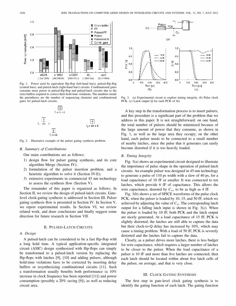
The power benefit of a pulsed-latch circuit is apparentfrom Fig. 1, which shows the result of an experiment thatwe performed in 45 nm technology: it demonstrates how thepower consumption of sequencing elements is greatly reducedwhen pulsed-latches are used instead of flip-flops. (Fig. 1 alsoshows that pulsed-flip-flop circuits provide a somewhat lesser
Manuscript received August 27, 2011; revised November 30, 2011;accepted January 3, 2012. Date of current version June 20, 2012.A preliminary version of this paper [1] was presented at the Asiaand South Pacific Design Automation Conference, Yokohama, Japan,January 25–28, 2011. This work was supported in part by theMid-Career Researcher Program through NRF Grant funded by the MEST(2011-0029087), and by Samsung Electronics. This paper was recommendedby Associate Editor I. Bahar.
S. Paik was with the Department of Electrical Engineering, KoreaAdvanced Institute of Science and Technology, Daejeon 305-701, Korea.He is now with Synopsys, Inc., Mountain View, CA 94043 USA (e-mail:[email protected]).
I. Han, S. Kim, and Y. Shin are with the Department of ElectricalEngineering, Korea Advanced Institute of Science and Technology, Daejeon305-701, Korea (e-mail: [email protected]; [email protected];[email protected]).
Digital Object Identifier 10.1109/TCAD.2012.2185235
benefit.) Notice that pulsers use a substantial amount of power,and so their use should be minimized, which is an importantobservation that motivates the work reported in this paper.
Clock gating is a standard way of reducing clocking power.It can be applied either at the register transfer level (RTL)or at the gate level. Using the former approach, registers thatare amenable to clock gating, such as load-enabled registers,are identified and clock gating can then be applied fairlysimply [5]; but this procedure makes the designer responsiblefor specifying the candidate registers for clock gating. Withthe latter approach, the logic that identifies the conditionunder which a clock can be gated, called the gating logicor gating function, is automatically synthesized [6]–[8]. Gate-level clock gating is more general and can complement theRTL technique, since it can be applied to any registers,including these which are not load-enabled. An importantproblem in gate-level clock gating is to identify groups ofregisters within which the registers of each group can be gatedtogether.
A. Motivation and Problem Statement
In pulsed-latch circuits, clock gating is realized by disablingpulsers, without introducing any extra circuitry such as clock-gating cells. (Circuit level details are presented in Section V.)This implies that the gate-level clock-gating synthesis ofpulsed-latch circuits, which we will call pulser gating syn-thesis, needs to group latches in such a way that the latchesin a group are sufficiently close together to be driven by asingle pulser, and also that they can be gated together (by thatpulser) as often as possible.
Fig. 2 illustrates the problem. We assume that the locationof the latches is known; and fi denotes the gating functionof latch i. When more than one latch is driven by a singlepulser, that pulser is enabled and disabled by an aggregategating function, e.g., if latches 1 and 2 are driven by a singlepulser, then f1 ∧ f2 = ab is its gating function. Thus it isimportant to group latches with similar gating functions, sothat an aggregate gating function can disable a pulser as oftenas possible. A counter-example is provided by latches 1 and3 in Fig. 2: if they are driven by the same pulser, then thatpulser will rarely be disabled.
We need to take account of the maximum load capacitancethat can be driven by a pulser, so that the pulse it generates isnot distorted. This requires us to accept a conservative limit onthe load capacitance, which then affects the number of latchesthat a pulser can drive and the lengths of the wires to connectthe pulser to its latches. In Fig. 2, latches 2 and 4 may notbe grouped, since they are located too far apart, even thoughtheir gating functions are similar.
0278-0070/$31.00 c© 2012 IEEE
1020 IEEE TRANSACTIONS ON COMPUTER-AIDED DESIGN OF INTEGRATED CIRCUITS AND SYSTEMS, VOL. 31, NO. 7, JULY 2012
Fig. 1. Power used by equivalent flip-flop (left-hand bars), pulsed-flip-flop(central bars), and pulsed-latch (right-hand bars) circuits. Combinational gatesconsume more power in pulsed-flip-flop and pulsed-latch circuits due to theextra buffers required to correct their hold-time violations. The numbers insidethe parentheses are the number of sequencing elements and combinationalgates for pulsed-latch circuits.
Fig. 2. Illustrative example of the pulser gating synthesis problem.
B. Summary of Contributions
Our main contributions are as follows:1) design flow for pulser gating synthesis, and its core
algorithm Merge (Section IV);2) formulation of the pulser insertion problem, and a
heuristic algorithm to solve it (Section IV-E);3) extensive experiments in commercial 45 nm technology
to assess the synthesis flow (Section V).The remainder of this paper is organized as follows. In
Section II, we review the design of pulsed-latch circuits. Gate-level clock-gating synthesis is addressed in Section III. Pulsergating synthesis flow is presented in Section IV. In Section V,we report experimental results. In Section VI, we reviewrelated work, and draw conclusions and finally suggest somedirection for future research in Section VII.
II. Pulsed-Latch Circuits
A. Design
A pulsed-latch can be considered to be a fast flip-flop witha long hold time. A typical application-specific integratedcircuit (ASIC) design synthesized with flip-flops can simplybe transformed to a pulsed-latch version by replacing theflip-flops with latches [9], [10] and adding pulsers, althoughhold-time violations have to be corrected by inserting delaybuffers or resynthesizing combinational circuits [11]. Sucha transformation usually benefits both performance (a 10%increase in clock frequency has been reported [11]) and powerconsumption (possibly a 20% saving [9]), as well as reducingcircuit area.
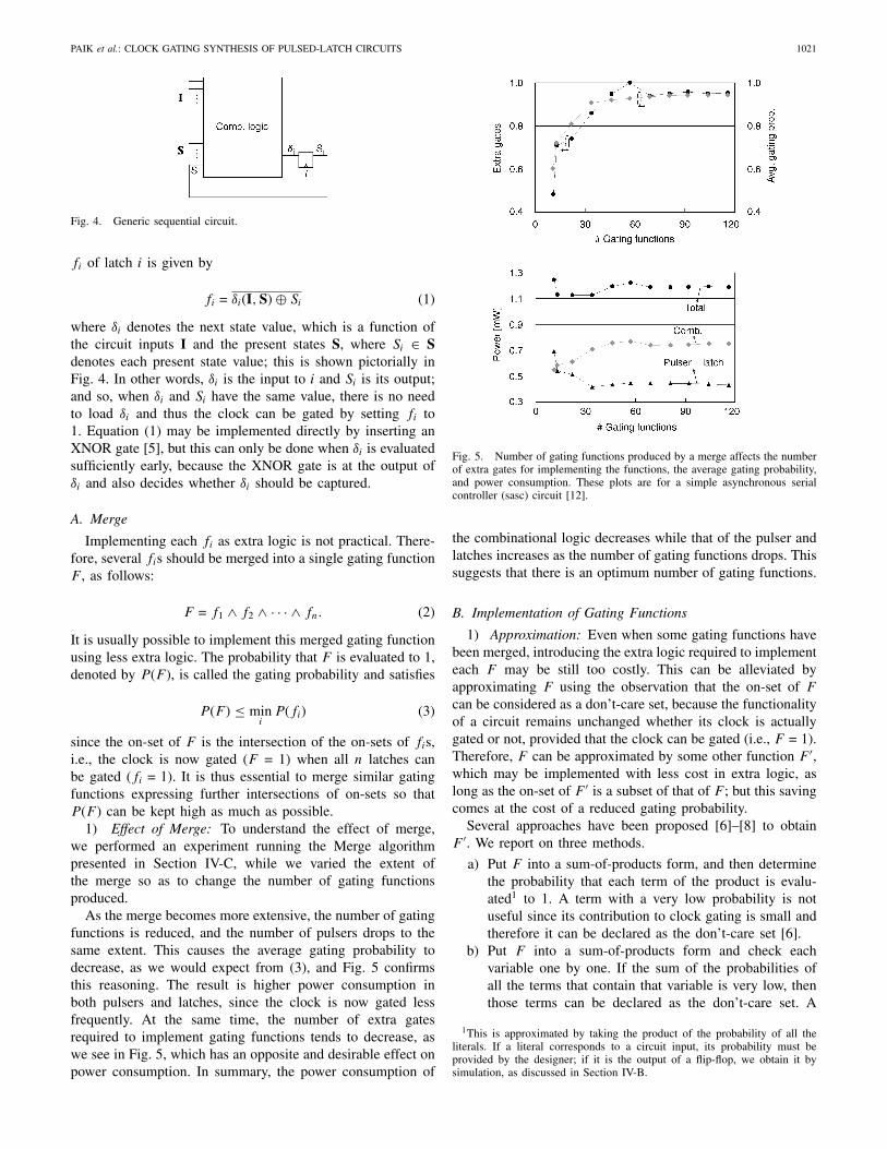
Fig. 3. (a) Experimental circuit to explore timing integrity. (b) Pulse clockPCK. (c) Latch output Q for each PCK of (b).
A key step in the transformation process is to insert pulsers,and this procedure is a significant part of the problem that weaddress in this paper. It is not straightforward: on one hand,the total number of pulsers should be minimized because ofthe large amount of power that they consume, as shown inFig. 1, as well as the large area they occupy; on the otherhand, each pulser needs to be connected to a small numberof nearby latches, since the pulse that it generates can easilybecome distorted if it is too heavily loaded.
B. Timing Integrity
Fig. 3(a) shows an experimental circuit designed to illustratethe importance of pulse shape in the operation of pulsed-latchcircuits. An example pulser was designed in 45-nm technologyto generate a pulse of 110 ps width with a slew of 40 ps, for aload capacitance of 10 fF or smaller. It was connected to tenlatches, which provide 6 fF of capacitance. This allows thewire capacitance, denoted by Cw, to be as high as 4 fF.
Fig. 3(b) shows a set of SPICE waveforms of the pulse clockPCK, when the pulser is loaded by 10, 15, and 50 fF, which weachieved by adjusting the value of Cw. The corresponding latchoutput for a falling latch input is shown in Fig. 3(c). Whenthe pulser is loaded by 10 fF, both PCK and the latch outputare nicely generated. At a load capacitance of 15 fF, PCK isslightly distorted; the latches are still able to capture the databut their clock-to-Q delay has increased by 10%, which maycause a timing problem. With a load of 50 fF, PCK is severelydistorted and the latches fail to capture the data.
Clearly, as a pulser drives more latches, there is less budgetfor wire capacitance, which requires a larger number of latchesto be closer to the pulser. When the load capacitance of apulser is 10 fF and more than five latches are connected, theneach latch should be located within about five latch cells ofthe pulser, on average, and that is very close.
III. Clock Gating Synthesis
The first step in gate-level clock gating synthesis is toidentify the gating function of each latch. The gating function
PAIK et al.: CLOCK GATING SYNTHESIS OF PULSED-LATCH CIRCUITS 1021
Fig. 4. Generic sequential circuit.
fi of latch i is given by
fi = δi(I, S) ⊕ Si (1)
where δi denotes the next state value, which is a function ofthe circuit inputs I and the present states S, where Si ∈ Sdenotes each present state value; this is shown pictorially inFig. 4. In other words, δi is the input to i and Si is its output;and so, when δi and Si have the same value, there is no needto load δi and thus the clock can be gated by setting fi to1. Equation (1) may be implemented directly by inserting anXNOR gate [5], but this can only be done when δi is evaluatedsufficiently early, because the XNOR gate is at the output ofδi and also decides whether δi should be captured.
A. Merge
Implementing each fi as extra logic is not practical. There-fore, several fis should be merged into a single gating functionF , as follows:
F = f1 ∧ f2 ∧ · · · ∧ fn. (2)
It is usually possible to implement this merged gating functionusing less extra logic. The probability that F is evaluated to 1,denoted by P(F ), is called the gating probability and satisfies
P(F ) ≤ mini
P(fi) (3)
since the on-set of F is the intersection of the on-sets of fis,i.e., the clock is now gated (F = 1) when all n latches canbe gated (fi = 1). It is thus essential to merge similar gatingfunctions expressing further intersections of on-sets so thatP(F ) can be kept high as much as possible.
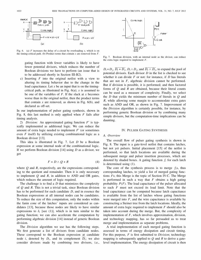
1) Effect of Merge: To understand the effect of merge,we performed an experiment running the Merge algorithmpresented in Section IV-C, while we varied the extent ofthe merge so as to change the number of gating functionsproduced.
As the merge becomes more extensive, the number of gatingfunctions is reduced, and the number of pulsers drops to thesame extent. This causes the average gating probability todecrease, as we would expect from (3), and Fig. 5 confirmsthis reasoning. The result is higher power consumption inboth pulsers and latches, since the clock is now gated lessfrequently. At the same time, the number of extra gatesrequired to implement gating functions tends to decrease, aswe see in Fig. 5, which has an opposite and desirable effect onpower consumption. In summary, the power consumption of
Fig. 5. Number of gating functions produced by a merge affects the numberof extra gates for implementing the functions, the average gating probability,and power consumption. These plots are for a simple asynchronous serialcontroller (sasc) circuit [12].
the combinational logic decreases while that of the pulser andlatches increases as the number of gating functions drops. Thissuggests that there is an optimum number of gating functions.
B. Implementation of Gating Functions
1) Approximation: Even when some gating functions havebeen merged, introducing the extra logic required to implementeach F may be still too costly. This can be alleviated byapproximating F using the observation that the on-set of F
can be considered as a don’t-care set, because the functionalityof a circuit remains unchanged whether its clock is actuallygated or not, provided that the clock can be gated (i.e., F = 1).Therefore, F can be approximated by some other function F ′,which may be implemented with less cost in extra logic, aslong as the on-set of F ′ is a subset of that of F ; but this savingcomes at the cost of a reduced gating probability.
Several approaches have been proposed [6]–[8] to obtainF ′. We report on three methods.
a) Put F into a sum-of-products form, and then determinethe probability that each term of the product is evalu-ated1 to 1. A term with a very low probability is notuseful since its contribution to clock gating is small andtherefore it can be declared as the don’t-care set [6].
b) Put F into a sum-of-products form and check eachvariable one by one. If the sum of the probabilities ofall the terms that contain that variable is very low, thenthose terms can be declared as the don’t-care set. A
1This is approximated by taking the product of the probability of all theliterals. If a literal corresponds to a circuit input, its probability must beprovided by the designer; if it is the output of a flip-flop, we obtain it bysimulation, as discussed in Section IV-B.
1022 IEEE TRANSACTIONS ON COMPUTER-AIDED DESIGN OF INTEGRATED CIRCUITS AND SYSTEMS, VOL. 31, NO. 7, JULY 2012
Fig. 6. (a) F increases the delay of a circuit by overloading x, which is onthe timing-critical path. (b) Product terms that contain x are removed from F .
gating function with fewer variables is likely to havefewer potential divisors, which reduces the number ofBoolean divisions we have to perform (an issue that isto be addressed shortly in Section III-B2).
c) Inserting F into the original netlist with a view toaltering its timing behavior due to the change in theload capacitance. Let x be an input that is on the timing-critical path, as illustrated in Fig. 6(a); x is assumed tobe one of the variables of F . If the slack at x becomesworse than in the original netlist, then the product termsthat contain x are removed, as shown in Fig. 6(b), anddeclared as off-set.
In our implementation of pulser gating synthesis, shown inFig. 8, this last method is only applied when F fails aftertiming analysis.
2) Division: An approximated gating function F ′ is typ-ically implemented as additional logic. We can reduce theamount of extra logic needed to implement F ′ (or sometimeseven F itself) by utilizing existing combinational logic as aBoolean divisor [13].
This idea is illustrated in Fig. 7. Let D be a Booleanexpression at some internal node of the combinational logic.If we perform Boolean division [14] using D as a divisor, weget
F = D ∧ Q + R (4)
where Q and R, respectively, are the expressions correspond-ing to the quotient and remainder. Then it is only necessaryto implement Q and R, in addition to AND and OR gates,which reduces the amount of logic required.
The challenge is to find a D that minimizes the complexityof Q and R. This is not a trivial task, since Boolean divisionhas to be performed for each candidate D, and in essence theBoolean expressions at all internal nodes can be candidates.To reduce the size of this computation, only the nodes withinthe fanin cone of the latches’ inputs are considered as can-didates [13], because those nodes are likely to have similarexpressions to δi [see (1)], which is in turn similar to thegating function; we can also accelerate the computation byperforming algebraic division [14] instead of generic Booleandivision.
The Division algorithm we use has the following steps.We first generate a list of divisors from candidate nodes.These correspond to the Boolean expression at candidatenode i, denoted by Di, and its complement Di; we alsoconsider divisors made by combining two divisors, i.e.,
Fig. 7. Boolean division, with an internal node as the divisor, can reducethe extra logic required to implement F .
Di +Dj, Di + Dj, Di ∧Dj , and Di ∧ Dj , to expand the pool ofpotential divisors. Each divisor D in the list is checked to seewhether it can divide F or not: for instance, if D has literalsthat are not in F , algebraic division cannot be performed.But if division is possible, it is performed; and then factoredforms of Q and R are obtained, because their literal countscan be used as a measure of complexity. Finally, we selectthe D that yields the minimum number of literals in Q andR, while allowing some margin to accommodate extra gatessuch as AND and OR, as shown in Fig. 7. Improvement ofthe Division algorithm is certainly possible, for instance, byperforming generic Boolean division or by combining manysimple divisors, but the computation-time implications can bedaunting.
IV. Pulser Gating Synthesis
A. Overview
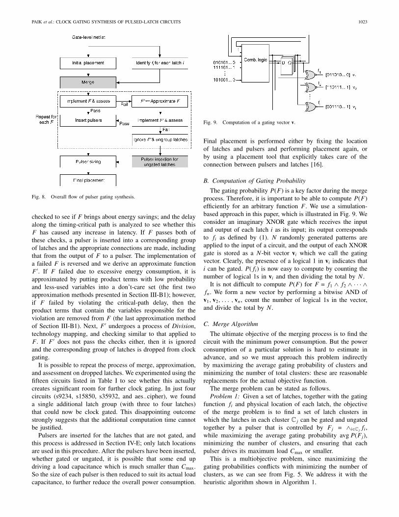
The overall flow of pulser gating synthesis is shown inFig. 8. The input is a gate-level netlist that contains latches,but not yet pulsers. Initial placement [15] of the netlist isperformed, so that latch locations are available during thesubsequent merge and pulser insertion processes, which aredenoted by shaded boxes. A gating function fi for each latchis determined using (1).
The core of the synthesis process is to merge fis, thuscorresponding latches, to yield a list of merged gating func-tions Fs; this Merge is the topic of Section IV-C. The Mergeis performed in such a way that F obtains a high gatingprobability P(F ). The load capacitance of the pulser allocatedto each F must not exceed its load limit. Note that theload capacitance can be computed because latch capacitanceis available from the list of latches whose gating functionswere merged into F , and the wire capacitance is available byconstructing a Steiner tree from the latch locations. Ideally, theamount of extra logic required to implement F should also betaken into account during the merge. But, the complexity ofimplementation of F , which involves approximation, division,and technology mapping, has so far persuaded us to treatmerge and implementation as separate problems.
A trial implementation of each merged gating function isassessed in terms of energy dissipation and circuit timing.For this purpose, F is first submitted to Division; technologymapping is subsequently applied to Q and R to derive a gate-level implementation. The energy dissipation of circuit is then
PAIK et al.: CLOCK GATING SYNTHESIS OF PULSED-LATCH CIRCUITS 1023
Fig. 8. Overall flow of pulser gating synthesis.
checked to see if F brings about energy savings; and the delayalong the timing-critical path is analyzed to see whether thisF has caused any increase in latency. If F passes both ofthese checks, a pulser is inserted into a corresponding groupof latches and the appropriate connections are made, includingthat from the output of F to a pulser. The implementation ofa failed F is reversed and we derive an approximate functionF ′. If F failed due to excessive energy consumption, it isapproximated by putting product terms with low probabilityand less-used variables into a don’t-care set (the first twoapproximation methods presented in Section III-B1); however,if F failed by violating the critical-path delay, then theproduct terms that contain the variables responsible for theviolation are removed from F (the last approximation methodof Section III-B1). Next, F ′ undergoes a process of Division,technology mapping, and checking similar to that applied toF . If F ′ does not pass the checks either, then it is ignoredand the corresponding group of latches is dropped from clockgating.
It is possible to repeat the process of merge, approximation,and assessment on dropped latches. We experimented using thefifteen circuits listed in Table I to see whether this actuallycreates significant room for further clock gating. In just fourcircuits (s9234, s15850, s35932, and aes−cipher), we founda single additional latch group (with three to four latches)that could now be clock gated. This disappointing outcomestrongly suggests that the additional computation time cannotbe justified.
Pulsers are inserted for the latches that are not gated, andthis process is addressed in Section IV-E; only latch locationsare used in this procedure. After the pulsers have been inserted,whether gated or ungated, it is possible that some end updriving a load capacitance which is much smaller than Cmax.So the size of each pulser is then reduced to suit its actual loadcapacitance, to further reduce the overall power consumption.
Fig. 9. Computation of a gating vector v.
Final placement is performed either by fixing the locationof latches and pulsers and performing placement again, orby using a placement tool that explicitly takes care of theconnection between pulsers and latches [16].
B. Computation of Gating Probability
The gating probability P(F ) is a key factor during the mergeprocess. Therefore, it is important to be able to compute P(F )efficiently for an arbitrary function F . We use a simulation-based approach in this paper, which is illustrated in Fig. 9. Weconsider an imaginary XNOR gate which receives the inputand output of each latch i as its input; its output correspondsto fi as defined by (1). N randomly generated patterns areapplied to the input of a circuit, and the output of each XNORgate is stored as a N-bit vector vi which we call the gatingvector. Clearly, the presence of a logical 1 in vi indicates thati can be gated. P(fi) is now easy to compute by counting thenumber of logical 1s in vi and then dividing the total by N.
It is not difficult to compute P(F ) for F = f1 ∧ f2 ∧ · · · ∧fn. We form a new vector by performing a bitwise AND ofv1, v2, . . . , vn, count the number of logical 1s in the vector,and divide the total by N.
C. Merge Algorithm
The ultimate objective of the merging process is to find thecircuit with the minimum power consumption. But the powerconsumption of a particular solution is hard to estimate inadvance, and so we must approach this problem indirectlyby maximizing the average gating probability of clusters andminimizing the number of total clusters: these are reasonablereplacements for the actual objective function.
The merge problem can be stated as follows.Problem 1: Given a set of latches, together with the gating
function fi and physical location of each latch, the objectiveof the merge problem is to find a set of latch clusters inwhich the latches in each cluster Cj can be gated and ungatedtogether by a pulser that is controlled by Fj = ∧i∈Cj
fi,while maximizing the average gating probability avg P(Fj),minimizing the number of clusters, and ensuring that eachpulser drives its maximum load Cmax or smaller.
This is a multiobjective problem, since maximizing thegating probabilities conflicts with minimizing the number ofclusters, as we can see from Fig. 5. We address it with theheuristic algorithm shown in Algorithm 1.
1024 IEEE TRANSACTIONS ON COMPUTER-AIDED DESIGN OF INTEGRATED CIRCUITS AND SYSTEMS, VOL. 31, NO. 7, JULY 2012
Algorithm 1 Merge algorithm
L1 Create a graph G(V, E, w)L2 Fi ← fi for each latch i
L3 while E �= ∅ doL4 Select eij of maximum Mij
L5 if C(i ∪ j) ≤ Cmax thenL6 i ← i ∪ j, Fi ← Fi ∧ Fj
L7 E ← E − {eix, ejy}, ∀x ∈ Ai − Aj, y ∈ Aj
L8 Update w(eix), ∀x ∈ Ai ∩ Aj
L9 else E ← E − {eij}
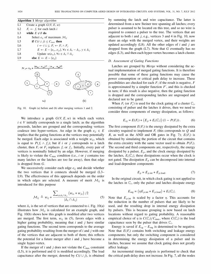
Fig. 10. Graph (a) before and (b) after merging vertices 1 and 2.
We introduce a graph G(V, E, w) in which each vertexi ∈ V initially corresponds to a single latch; as the algorithmproceeds, latches are grouped and the corresponding verticescoalesce into hyper-vertices. An edge in the graph eij ∈ E
implies that the gating functions at the vertices may potentiallybe merged. Each edge is associated with a weight wij , whichis equal to P(fi ∧ fj); but if i or j corresponds to a latchcluster, then Fi or Fj replaces fi or fj . Initially, every pair ofvertices is nominally linked by an edge. However, if mergingis likely to violate the Cmax condition (i.e., i or j contains toomany latches or the latches are too far away), then that edgeis dropped from G.
We successively consider each edge eij and decide whetherthe two vertices that it connects should be merged (L3–L9). The effectiveness of this approach depends on the orderin which edges are selected. A measure of merit Mij isintroduced for this purpose
Mij � wij +
∑x∈Ai∩Aj
(wix + wjx
)/2
|Ai ∩ Aj| (5)
where Ai is the set of vertices that are connected to i. Fig. 10(a)illustrates how Mij is calculated for an example graph, andFig. 10(b) shows how this graph is modified after two verticesare merged. The first term, wij in (5), favors edges with ahigher gating probability, meaning that i and j have similargating functions. The second term corresponds to the averagegating probability resulting from the merger of i and j with oneof the vertices that are adjacent to both of them; this reflectsthe potential for a future merger after i and j have become asingle hyper-vertex.
If the merger of i and j does not violate the Cmax constraint(L5), it is performed and G is modified accordingly. The loadcapacitance after the merger, denoted by C(i ∪ j), is obtained
by summing the latch and wire capacitance. The latter isdetermined from a new Steiner tree spanning all latches; everypulser is assumed to be located on this tree, and so no wire isrequired to connect a pulser to the tree. The vertices that areadjacent to both i and j, e.g., vertices 3 and 4 in Fig. 10, nowshare an edge with the merged vertex, and their weights areupdated accordingly (L8). All the other edges of i and j aredropped from the graph (L7). Note that G eventually has noedges (L3), and then each hyper-vertex becomes a latch cluster.
D. Assessment of Gating Functions
Latches are grouped by Merge without considering the ac-tual implementation of merged gating functions. It is thereforepossible that some of these gating functions may cause thepower consumption or critical path delay to increase. Thesepossibilities are checked for each F ; if the result is negative, F
is approximated by a simpler function F ′, and this is checkedin turn; if this result is also negative, then the gating functionis dropped and the corresponding latches are ungrouped anddeclared not to be gated.
When Fi (or F ′i ) is used for the clock gating of a cluster Ci,
consisting of pulser and the latches it drives, then we need toconsider three components of energy dissipation, as follows:
Ecg = E(Fi) +(Ep + El|Ci|
)(1 − P(Fi)) . (6)
The first component E(Fi) is the energy dissipated by the extracircuitry required to implement Fi (this corresponds to Q andR, as well as the AND and OR gates in Fig. 7); E(Fi) isobtained by simulating the portion of the circuit that containsthe extra circuitry with the same vector used to obtain P(Fi).The second and third components are, respectively, the energydissipated by a pulser, Ep, and the clock energy dissipated bythe latches, El|Ci|; these dissipations occur when the clock isnot gated. The dissipation Ep can be decomposed into internaland load-dependent components
Ep = Ep,int + Ep,load. (7)
In the original circuit, in which clock gating is not applied tothe latches in Ci, only the pulser and latches dissipate energy
Eorg =(ηEp,int + Ep,load
)+ El|Ci|. (8)
Note that Ep,int is scaled by a factor η. This accounts forthe reduction in the number of pulsers that are likely to beused, and the resulting drop in internal energy dissipationby pulsers. This is because grouping is now based on latchlocations without regard to gating probability. A reasonableempirical choice of η is C(Ci)/Cmax, where C(Ci) is the loadcapacitance seen by the pulser that drives Ci.
Energy is saved if Ecg − Eorg is determined to be negative.Note that E(Fi) contains both switching and leakage energycomponents; but only the switching component is consideredin determining the energy dissipation of a pulser and itslatches, because we assume that clock gating does not greatlyaffect leakage.
An incremental timing analysis is performed to check thatthe critical path delay does not increase. In Fig. 7, all the nodes
PAIK et al.: CLOCK GATING SYNTHESIS OF PULSED-LATCH CIRCUITS 1025
Algorithm 2 Pulser Insertion algorithm
L1 Create a graph Gc(V, E, w)L2 while E �= ∅ doL3 Select eij of minimum wij
L4 if C(i ∪ j) ≤ Cmax thenL5 i ← i ∪ j
L6 E ← E − {eix, ejy}, ∀x ∈ Ai − Aj, y ∈ Aj
L7 else E ← E − {eij}
that are within the fanout cone of D, as well as Q and R, aresubmitted to timing analysis.
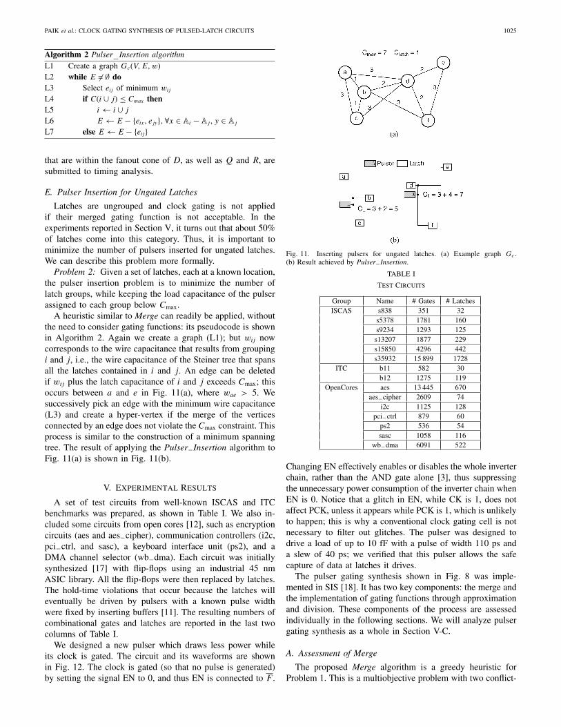
E. Pulser Insertion for Ungated Latches
Latches are ungrouped and clock gating is not appliedif their merged gating function is not acceptable. In theexperiments reported in Section V, it turns out that about 50%of latches come into this category. Thus, it is important tominimize the number of pulsers inserted for ungated latches.We can describe this problem more formally.
Problem 2: Given a set of latches, each at a known location,the pulser insertion problem is to minimize the number oflatch groups, while keeping the load capacitance of the pulserassigned to each group below Cmax.
A heuristic similar to Merge can readily be applied, withoutthe need to consider gating functions: its pseudocode is shownin Algorithm 2. Again we create a graph (L1); but wij nowcorresponds to the wire capacitance that results from groupingi and j, i.e., the wire capacitance of the Steiner tree that spansall the latches contained in i and j. An edge can be deletedif wij plus the latch capacitance of i and j exceeds Cmax; thisoccurs between a and e in Fig. 11(a), where wae > 5. Wesuccessively pick an edge with the minimum wire capacitance(L3) and create a hyper-vertex if the merge of the verticesconnected by an edge does not violate the Cmax constraint. Thisprocess is similar to the construction of a minimum spanningtree. The result of applying the Pulser−Insertion algorithm toFig. 11(a) is shown in Fig. 11(b).
V. Experimental Results
A set of test circuits from well-known ISCAS and ITCbenchmarks was prepared, as shown in Table I. We also in-cluded some circuits from open cores [12], such as encryptioncircuits (aes and aes−cipher), communication controllers (i2c,pci−ctrl, and sasc), a keyboard interface unit (ps2), and aDMA channel selector (wb−dma). Each circuit was initiallysynthesized [17] with flip-flops using an industrial 45 nmASIC library. All the flip-flops were then replaced by latches.The hold-time violations that occur because the latches willeventually be driven by pulsers with a known pulse widthwere fixed by inserting buffers [11]. The resulting numbers ofcombinational gates and latches are reported in the last twocolumns of Table I.
We designed a new pulser which draws less power whileits clock is gated. The circuit and its waveforms are shownin Fig. 12. The clock is gated (so that no pulse is generated)by setting the signal EN to 0, and thus EN is connected to F .
Fig. 11. Inserting pulsers for ungated latches. (a) Example graph Gc.(b) Result achieved by Pulser−Insertion.
TABLE I
Test Circuits
Group Name # Gates # LatchesISCAS s838 351 32
s5378 1781 160s9234 1293 125
s13207 1877 229s15850 4296 442s35932 15 899 1728
ITC b11 582 30b12 1275 119
OpenCores aes 13 445 670aes−cipher 2609 74
i2c 1125 128pci−ctrl 879 60
ps2 536 54sasc 1058 116
wb−dma 6091 522
Changing EN effectively enables or disables the whole inverterchain, rather than the AND gate alone [3], thus suppressingthe unnecessary power consumption of the inverter chain whenEN is 0. Notice that a glitch in EN, while CK is 1, does notaffect PCK, unless it appears while PCK is 1, which is unlikelyto happen; this is why a conventional clock gating cell is notnecessary to filter out glitches. The pulser was designed todrive a load of up to 10 fF with a pulse of width 110 ps anda slew of 40 ps; we verified that this pulser allows the safecapture of data at latches it drives.
The pulser gating synthesis shown in Fig. 8 was imple-mented in SIS [18]. It has two key components: the merge andthe implementation of gating functions through approximationand division. These components of the process are assessedindividually in the following sections. We will analyze pulsergating synthesis as a whole in Section V-C.
A. Assessment of Merge
The proposed Merge algorithm is a greedy heuristic forProblem 1. This is a multiobjective problem with two conflict-

1026 IEEE TRANSACTIONS ON COMPUTER-AIDED DESIGN OF INTEGRATED CIRCUITS AND SYSTEMS, VOL. 31, NO. 7, JULY 2012
Fig. 12. Pulser and its SPICE waveforms.
ing goals: maximizing the average gating probability and min-imizing the number of clusters (thus the number of pulsers).
We generated a set of Pareto reference points for verysmall examples such as b11. Fixing the latch locations, wegenerated all possible latch clusters by manipulating the graphG introduced in Section IV-C; we first make each latcha cluster; then clusters with two latches are generated bycombining two single-latch clusters which share an edge inG, if the new cluster satisfies the Cmax constraint. Clusterswith more latches are generated in a similar way, until nomore new clusters can be formed without violating the Cmax
constraint.Each of the resulting N clusters is associated with a decision
variable xi and its gating probability Pi is also determined.We want to choose M clusters with the highest gating prob-abilities. This choice can be formulated as an integer linearprogramming (ILP) problem with the objective function
MaximizeN∑
i=0
Pixi (9)
which maximizes the average gating probability. We are goingto pick only M clusters
N∑
i=0
xi = M (10)
and each latch has to be included in one and only one cluster
∑
∀i that contains j
xi = 1 for each latch j. (11)
We now vary M and solve the ILP problem for each instance,producing a set of Pareto points; but this computation requiresa lot of time and memory, and can therefore be applied to verysmall circuits. Fig. 13 shows the Pareto points and the solutionobtained by the Merge algorithm for four example circuits.
For the three circuits, s400, b07, and b11, the solutionreturned by Merge appears to be close to the peak of thecurve generated by the Pareto points, which suggests that areasonable tradeoff has been achieved between the averagegating probability and the number of clusters. The curve foraes−cipher is comparatively flat, suggesting that its averagegating probability is not strongly affected by the constructionof clusters. We found that many latches in aes−cipher have
Fig. 13. Pareto points and the solution returned by the Merge heuristic.
TABLE II
Number of Extra Gates to Implement Gating Functions
Without and With Using Division
Circuit # Gating # Extra GatesFunctions Without With Diff. (%)
Division Divisions838 5 24 14 −41.7s5378 7 106 106 –s9234 8 130 103 −20.8s13207 27 443 423 −4.5s15850 40 545 517 −5.1s35932 277 2272 2272 –b11 3 27 27 –b12 11 238 230 −3.4aes 25 355 329 −7.3aes−cipher 8 86 86 –i2c 10 181 166 −8.3pci−ctrl 2 120 85 −29.2ps2 1 15 15 –sasc 15 165 165 –wb−dma 32 591 485 −17.9Average −9.2
similar gating functions (46% of pairs of the latches havemerged gating function with probabilities of 0.7 or more), sothe average gating probability does not drop dramatically evenif a cluster contains many latches.
B. Assessment of Implementation of Gating Functions
The implementation of a gating function F can be followedby two possible procedures (see Fig. 8): either we applyDivision to F , check if there is an energy saving and thetiming-critical path remains intact, and then implement Q andR if F passes these checks; or we can approximate F by F ′,apply Division to F ′, check F ′, and implement as before.
To assess the effectiveness of the Division algorithm, wecollected all the gating functions, either F or F ′, that passedthe check when they were implemented without using Divi-sion: in this case “Implement” in Fig. 8 becomes the directimplementation of the gating function. The numbers of thesegating functions are listed in the second column of Table II;and column 3 contains the number of extra gates requiredfor direct implementation of the gating functions. Division is
PAIK et al.: CLOCK GATING SYNTHESIS OF PULSED-LATCH CIRCUITS 1027
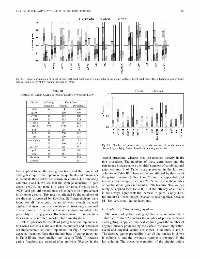
Fig. 14. Power consumption of initial circuits (left-hand bars) and of circuits after pulser gating synthesis (right-hand bars). The reduction in power drawnranges from 0.1% to 58.0%, with an average of 19.8%.
TABLE III
Number of Extra Gates in Pulser Gating Synthesis Flow
Circuit # Gating Extra GatesFunctions Number Percentage
s838 6 14 4.0s5378 7 106 6.0s9234 8 103 8.0s13207 27 415 22.1s15850 40 517 12.0s35932 277 2272 14.3
b11 3 27 4.6b12 11 230 18.0aes 25 329 2.4
aes−cipher 8 86 3.3i2c 10 166 14.8
pci−ctrl 2 85 9.7ps2 6 47 8.8sasc 16 187 17.7
wb−dma 39 634 10.4Average 10.4
then applied to all the gating functions and the number ofextra gates required to implement the quotients and remaindersis counted; these totals are shown in column 4. Comparingcolumns 3 and 4, we see that the average reduction in gatecount is 9.2%, but there is a wide variation. Circuits s838,s9234, and pci−ctrl benefit most while there is no improvementin six other circuits. This result is affected by the goodness ofthe divisors discovered by Division. Sufficient divisors werefound for all the circuits we tested, even though we usedalgebraic division; but many of those divisors only containeda small number of literals, and were therefore discarded. Thepossibility of using generic Boolean division, if computationtimes can be controlled, merits future investigation.
Table III presents the results of gating function implementa-tion when Division is run and then the quotient and remainderare implemented: so that “Implement” in Fig. 8 recovers itsexpected meaning. Note that the numbers of gating functionsin Table III are never smaller than these in Table II, becausegating functions are assessed after applying Division in the
Fig. 15. Number of pulsers after synthesis, normalized to the numberobtained by applying Pulser−Insertion to the original netlist.
second procedure, whereas they are assessed directly in thefirst procedure. The numbers of these extra gates and thepercentage increase above the initial numbers of combinationalgates (column 3 of Table I) are presented in the last twocolumns of Table III. These results are affected by the size ofthe gating functions (either F or F ′) and the applicability ofDivision. For example, there is a 22.1% increase in the numberof combinational gates in circuit s13207 because Division canrarely be applied (see Table II). But the efficacy of Divisionis not always significant: the increase in gates is only 4.6%for circuit b11, even though Division is never applied, becauseb11 has very small gating functions.
C. Analysis of Pulser Gating Synthesis
The result of pulser gating synthesis is summarized inTable IV. Column 2 contains the number of pulsers to whichclock gating is applied; the next column gives the number ofungated pulsers produced by the Pulser−Insertion algorithm.Gated and ungated latches are shown in columns 4 and 5.The average gating probability over all the latches is shownin column 6, and the synthesis runtime is reported in thelast column. The power consumption of the circuits before
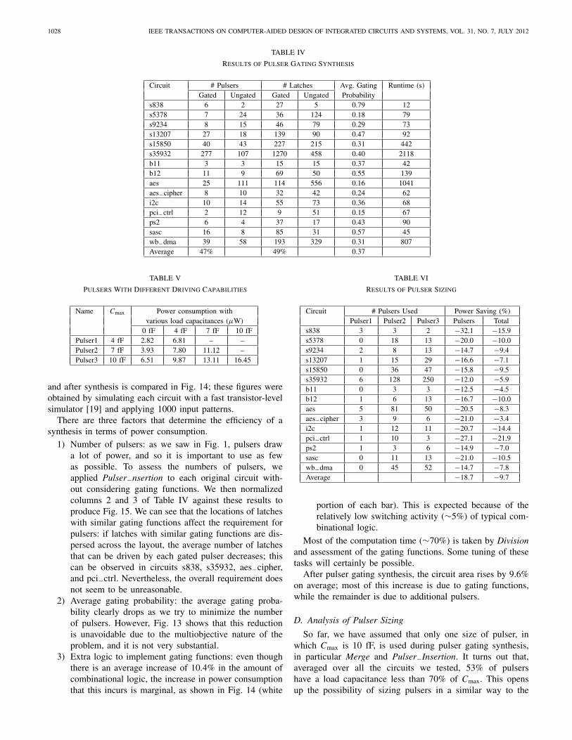
1028 IEEE TRANSACTIONS ON COMPUTER-AIDED DESIGN OF INTEGRATED CIRCUITS AND SYSTEMS, VOL. 31, NO. 7, JULY 2012
TABLE IV
Results of Pulser Gating Synthesis
Circuit # Pulsers # Latches Avg. Gating Runtime (s)Gated Ungated Gated Ungated Probability
s838 6 2 27 5 0.79 12s5378 7 24 36 124 0.18 79s9234 8 15 46 79 0.29 73s13207 27 18 139 90 0.47 92s15850 40 43 227 215 0.31 442s35932 277 107 1270 458 0.40 2118b11 3 3 15 15 0.37 42b12 11 9 69 50 0.55 139aes 25 111 114 556 0.16 1041aes−cipher 8 10 32 42 0.24 62i2c 10 14 55 73 0.36 68pci−ctrl 2 12 9 51 0.15 67ps2 6 4 37 17 0.43 90sasc 16 8 85 31 0.57 45wb−dma 39 58 193 329 0.31 807Average 47% 49% 0.37
TABLE V
Pulsers With Different Driving Capabilities
Name Cmax Power consumption withvarious load capacitances (μW)
0 fF 4 fF 7 fF 10 fFPulser1 4 fF 2.82 6.81 – –Pulser2 7 fF 3.93 7.80 11.12 –Pulser3 10 fF 6.51 9.87 13.11 16.45
and after synthesis is compared in Fig. 14; these figures wereobtained by simulating each circuit with a fast transistor-levelsimulator [19] and applying 1000 input patterns.
There are three factors that determine the efficiency of asynthesis in terms of power consumption.
1) Number of pulsers: as we saw in Fig. 1, pulsers drawa lot of power, and so it is important to use as fewas possible. To assess the numbers of pulsers, weapplied Pulser−nsertion to each original circuit with-out considering gating functions. We then normalizedcolumns 2 and 3 of Table IV against these results toproduce Fig. 15. We can see that the locations of latcheswith similar gating functions affect the requirement forpulsers: if latches with similar gating functions are dis-persed across the layout, the average number of latchesthat can be driven by each gated pulser decreases; thiscan be observed in circuits s838, s35932, aes−cipher,and pci−ctrl. Nevertheless, the overall requirement doesnot seem to be unreasonable.
2) Average gating probability: the average gating proba-bility clearly drops as we try to minimize the numberof pulsers. However, Fig. 13 shows that this reductionis unavoidable due to the multiobjective nature of theproblem, and it is not very substantial.
3) Extra logic to implement gating functions: even thoughthere is an average increase of 10.4% in the amount ofcombinational logic, the increase in power consumptionthat this incurs is marginal, as shown in Fig. 14 (white
TABLE VI
Results of Pulser Sizing
Circuit # Pulsers Used Power Saving (%)Pulser1 Pulser2 Pulser3 Pulsers Total
s838 3 3 2 −32.1 −15.9s5378 0 18 13 −20.0 −10.0s9234 2 8 13 −14.7 −9.4s13207 1 15 29 −16.6 −7.1s15850 0 36 47 −15.8 −9.5s35932 6 128 250 −12.0 −5.9b11 0 3 3 −12.5 −4.5b12 1 6 13 −16.7 −10.0aes 5 81 50 −20.5 −8.3aes−cipher 3 9 6 −21.0 −3.4i2c 1 12 11 −20.7 −14.4pci−ctrl 1 10 3 −27.1 −21.9ps2 1 3 6 −14.9 −7.0sasc 0 11 13 −21.0 −10.5wb−dma 0 45 52 −14.7 −7.8Average −18.7 −9.7
portion of each bar). This is expected because of therelatively low switching activity (∼5%) of typical com-binational logic.
Most of the computation time (∼70%) is taken by Divisionand assessment of the gating functions. Some tuning of thesetasks will certainly be possible.
After pulser gating synthesis, the circuit area rises by 9.6%on average; most of this increase is due to gating functions,while the remainder is due to additional pulsers.
D. Analysis of Pulser Sizing
So far, we have assumed that only one size of pulser, inwhich Cmax is 10 fF, is used during pulser gating synthesis,in particular Merge and Pulser−Insertion. It turns out that,averaged over all the circuits we tested, 53% of pulsershave a load capacitance less than 70% of Cmax. This opensup the possibility of sizing pulsers in a similar way to the
PAIK et al.: CLOCK GATING SYNTHESIS OF PULSED-LATCH CIRCUITS 1029
more usual gate sizing, so as to optimize power consumption,performance, and area.
We designed two smaller pulsers that will generate the samepulse as the 10 fF version (110 ps wide with 40 ps of slew),as long as their maximum load capacitances are not exceeded.Some characteristics of these new pulsers are given in Table V,where they are called Pulser1 and Pulser2; Pulser3 is theoriginal version. The power consumption data given in Table Vshows that a smaller pulser does use less power, as we expect.
The result of pulser sizing is shown in Table VI. On average,51% of the pulsers are now either Pulser1 or Pulser2 types;the latter proved especially useful. This change reduces pulserspower consumption by 18.7%, and the overall power usage by9.7%.
VI. Related Work
We will briefly review previous work related to gate-levelclock gating of pulsed-latch circuits.
A. Pulsed-Latch Methodology
There have been several research efforts to use pulsed-latches instead of flip-flops. It has been shown [9], [10] thatthe flip-flops in existing designs can be replaced with pulsed-latches to reduce dynamic power consumption; and selectivereplacement of flip-flops can reduce the timing overhead [20].In all these schemes, each pulser is buffered to drive manylatches; but there is no detailed discussion of the grouping oflatches to share a pulser more effectively. We take a differentline, and do not place buffers between a pulser and its latches,so that a pulser effectively serves as a leaf-level clock buffer.This strategy avoids the possibility of a pulse disappearingas it propagates through multiple buffers; but now pulserinsertion becomes an important problem (which we addressedin Section IV-E).
B. Gate-Level Clock Gating
In gate-level clock gating, gating functions can be auto-matically synthesized from a netlist [6]–[8]. Since the gatingfunction itself consumes power and area, effectiveness dependson controlling the implementation cost while achieving a highgating probability.
One way to reduce the implementation cost is to reusethe existing logic. Internal signals can be used as a Booleandivisor D to implement a gating function F given by F =D ∧ Q + R [13]. If some loss of gating probability can betolerated, a gating function can be approximated by summingthe internal nodes that are strictly contained in that func-tion [7]; this only requires an extra OR gate. There are severalother approaches to approximating F . If the probability of aparticular product term is low, it can be declared as a don’t-care set, and this reduces the size of the synthesized gatingfunction [6]. If some variables only make a small contributionto the gating probability, they can be removed from the supportof gating function [6]. When gating functions are describedusing a binary decision diagram (BDD), there is advantage ineliminating a portion of the BDD nodes below some gatingprobability threshold [21].
Merging gating functions across multiple flip-flops is alsoan effective way of reducing the implementation cost. Thishas been explored in the context of counters by means ofa simple grouping of neighboring bits [22]. A more generalalgorithm [13] randomly selects a gating function and greedilymerges other gating functions in pursuit of a heuristic objectivefunction. A similarity measure, which takes account of bothlogical similarity and physical distance, has also been proposedto guide merging [8]. Merging gating functions is also akey problem in clock gating of pulsed-latches; but existingalgorithms cannot be directly applied to our approach becauseof the Cmax constraint, which is why we have had to developa new heuristic algorithm.
VII. Conclusion
Gate-level clock gating synthesis can discover clock gatingconditions that are not specified by designers. We exploredgate-level clock gating synthesis of pulsed-latch circuits, inwhich a key problem is to group physically close latchesthat have similar gating functions. We showed that Booleandivision can reduce the amount of extra logic required toimplement gating functions, and the same approach can alsobe applied to general gate-level clock gating synthesis.
We can identify some of the further work needed to de-velop this concept. Currently, merge is performed withoutconsidering the complexity of the resulting gating functions;some way of quickly estimating that complexity would beof considerable value. Also, each gating function is currentlyimplemented separately; sharing logic between several gatingfunctions might well be advantageous. Finally, we noted thatpulser sizing is currently performed after optimization; in afuture investigation we might consider combining pulser sizingand pulser gating synthesis.
References
[1] S. Kim, I. Han, S. Paik, and Y. Shin, “Pulser gating: A clock gatingof pulsed-latch circuits,” in Proc. Asia South Pacific Des. Autom. Conf.,Jan. 2011, pp. 190–195.
[2] S. Kozu, M. Daito, Y. Sugiyama, H. Suzuki, H. Morita, M. Nomura,K. Nadehara, S. Ishibuchi, M. Tokuda, Y. Inoue, T. Nakayama, H. Hari-gai, and Y. Yano, “A 100 MHz, 0.4 W RISC processor with 200 MHzmultiply adder, using pulse-register technique,” in Proc. Int. Solid-StateCircuits Conf., Feb. 1996, pp. 140–141.
[3] S. Naffziger, G. Colon-Bonet, T. Fischer, R. Riedlinger, T. Sullivan, andT. Grutkowski, “The implementation of the Itanium 2 microprocessor,”IEEE J. Solid-State Circuits, vol. 37, no. 11, pp. 1448–1460, Nov. 2002.
[4] H. Partovi, R. Burd, U. Salim, F. Weber, L. DiGregorio, and D. Draper,“Flow-through latch and edge-triggered flip-flop hybrid elements,” inProc. Int. Solid-State Circuits Conf., Feb. 1996, pp. 138–139.
[5] Power Compiler User Guide, Synopsys, Inc., Mountain View, CA, Dec.2010.
[6] L. Benini, G. D. Micheli, E. Macii, M. Poncino, and R. Scarsi,“Symbolic synthesis of clock-gating logic for power optimization ofsynchronous controllers,” ACM Trans. Des. Autom. Electron. Syst.,vol. 4, no. 4, pp. 351–375, Oct. 1999.
[7] A. Hurst, “Automatic synthesis of clock gating logic with controllednetlist perturbation,” in Proc. Des. Autom. Conf., Jun. 2008, pp. 654–657.
[8] E. Arbel, C. Eisner, and O. Rokhlenko, “Resurrecting infeasible clock-gating functions,” in Proc. Des. Autom. Conf., Jul. 2009, pp. 160–165.
[9] S. Shibatani and A. Li, “Pulse-latch approach reduces dynamic power,”EE Times, Jul. 2006.
1030 IEEE TRANSACTIONS ON COMPUTER-AIDED DESIGN OF INTEGRATED CIRCUITS AND SYSTEMS, VOL. 31, NO. 7, JULY 2012
[10] H. Li, M. Chen, and K. Ho, “System and method of replacing flip-flopswith pulsed latches in circuit designs,” U.S. Patent 7 694 242 B1, Apr.2010.
[11] Y. Shin and S. Paik, “Pulsed-latch circuits: A new dimension in ASICdesign,” IEEE Des. Test Comput., vol. 28, no. 6, pp. 50–57, Nov. 2011.
[12] OpenCores [Online]. Available: http://www.opencores.org[13] F. Theeuwen and E. Seelen, “Power reduction through clock gating by
symbolic manipulation,” in Proc. IFIP Int. Workshop Logic ArchitectureSynthesis, 1996, pp. 184–191.
[14] R. Brayton, R. Rudell, A. Sangiovanni-Vincentelli, and A. Wang, “MIS:A multiple-level logic optimization system,” IEEE Trans. Comput.-AidedDes., vol. 6, no. 6, pp. 1062–1081, Nov. 1987.
[15] IC Compiler Implementation User Guide, Synopsys, Inc., MountainView, CA, Mar. 2010.
[16] Y. Chuang, S. Kim, Y. Shin, and Y. Chang, “Pulsed-latch-aware place-ment for timing-integrity optimization,” in Proc. Des. Autom. Conf., Jun.2010, pp. 280–285.
[17] Design Compiler User Guide, Synopsys, Inc., Mountain View, CA, Sep.2008.
[18] E. Sentovich, K. J. Singh, L. Lavagno, C. Moon, R. Murgai, A. Saldanha,H. Savoj, P. R. Stephan, R. K. Brayton, and A. Sangiovanni-Vincentelli,“SIS: A system for sequential circuit synthesis,” Univ. California,Berkeley, CA, Tech. Rep. UCB/ERL M92/41, May 1992.
[19] NanoSim User Guide, Synopsys, Inc., Mountain View, CA, Jun. 2009.[20] T. Baumann, D. Schmitt-Landsiedel, and C. Pacha, “Architectural assess-
ment of design techniques to improve speed and robustness in embeddedmicroprocessors,” in Proc. Des. Autom. Conf., Jul. 2009, pp. 947–950.
[21] U. Hinsberger, R. Kolla, and T. Kunjan, “Approximative representationof Boolean functions by size controllable ROBDDs,” Instit. Inform.,Univ. Wurzburg, Wurzburg, Germany, Tech. Rep. 182, Sep. 1997.
[22] P. Parra, A. Acosta, and M. Valencia, “Selective clock-gating for lowpower/low noise synchronous counters,” in Proc. 12th Int. WorkshopIntegr. Circuit Des., 2002, pp. 448–457.
Seungwhun Paik received the B.S. and Ph.D. de-grees in electrical engineering from the Departmentof Electrical Engineering, Korea Advanced Instituteof Science and Technology, Daejeon, Korea, in 2006and 2011, respectively.
He joined Synopsys, Inc., Mountain View, CA,in 2011, where he has been working on a timinganalysis tool. His current research interests includetiming analysis and optimization of very large scaleintegration circuits.
Dr. Paik has been a member of the TechnicalProgram Committee of ASP-DAC.
Inhak Han received the B.S. and M.S. degreesin electrical engineering from the Korea AdvancedInstitute of Science and Technology (KAIST), Dae-jeon, Korea, in 2010 and 2012, respectively. Heis currently pursuing the Ph.D. degree with theDepartment of Electrical Engineering, KAIST.
His current research interests include timing andthermal analysis for very large scale integrationcircuits and low-power design using clock gating andpulsed-latch.
Sangmin Kim received the B.S. and M.S. degreesin electrical engineering from the Korea AdvancedInstitute of Science and Technology (KAIST), Dae-jeon, Korea, in 2008 and 2010, respectively. Heis currently pursuing the Ph.D. degree with theDepartment of Electrical Engineering, KAIST.
His current research interests include computer-aided design for low-power design and pulsed-latchapplication-specific integrated circuit design.
Youngsoo Shin (M’00–SM’05) received the B.S.,M.S., and Ph.D. degrees in electronics engineeringfrom Seoul National University, Seoul, Korea.
From 2000 to 2001, he was a Research Asso-ciate with the University of Tokyo, Tokyo, Japan,and from 2001 to 2004 he was a Research StaffMember with the IBM T. J. Watson Research Center,Yorktown Heights, NY. He joined the Department ofElectrical Engineering, Korea Advanced Institute ofScience and Technology, Daejeon, Korea, in 2004,where he is currently an Associate Professor. His
current research interests include computer-aided design with emphasis onlow-power design and design tools, high-level synthesis, sequential synthesis,and programmable logic.
Dr. Shin has received several awards, including the Best Paper Award atthe 2005 International Symposium on Quality Electronic Design and the2002 IP Excellence Award from Japan. He has been a member of thetechnical program committees and organizing committees of many technicalconferences, including DAC, ICCAD, ISLPED, ASP-DAC, CASES, ISVLSI,and ISCAS. He is a member of the ACM SIGDA Low Power TechnicalCommittee and is an Associate Editor of the IEEE Transactions on
Computer-Aided Design of Integrated Circuits and Systems and theACM Transactions on Design Automation of Electronic Systems.


