04 geran bc-en-zxg10 i bsc structure and principle-1-training manual-201010 (1)
192
ZXG10 iBSC Structure and Principle ZTE UNIVERSITY ZTE University, Dameisha YanTian District, Shenzhen, P. R. China 518083 Tel: (86) 755 26778800 Fax: (86) 755 26778999 URL: http://ensupport.zte.com.cn E-mail: [email protected]
-
Upload
shelton-siziba -
Category
Documents
-
view
49 -
download
1
Transcript of 04 geran bc-en-zxg10 i bsc structure and principle-1-training manual-201010 (1)

ZXG10 iBSCStructure and Principle
ZTE UNIVERSITYZTE University, DameishaYanTian District, Shenzhen,P. R. China518083Tel: (86) 755 26778800Fax: (86) 755 26778999URL: http://ensupport.zte.com.cnE-mail: [email protected]

LEGAL INFORMATION
Copyright © 2010 ZTE CORPORATION.
The contents of this document are protected by copyright laws and international treaties. Any reproduction or distribution ofthis document or any portion of this document, in any form by any means, without the prior written consent of ZTE CORPO-RATION is prohibited. Additionally, the contents of this document are protected by contractual confidentiality obligations.
All company, brand and product names are trade or service marks, or registered trade or service marks, of ZTE CORPORATIONor of their respective owners.
This document is provided “as is”, and all express, implied, or statutory warranties, representations or conditions are dis-claimed, including without limitation any implied warranty of merchantability, fitness for a particular purpose, title or non-in-fringement. ZTE CORPORATION and its licensors shall not be liable for damages resulting from the use of or reliance on theinformation contained herein.
ZTE CORPORATION or its licensors may have current or pending intellectual property rights or applications covering the subjectmatter of this document. Except as expressly provided in any written license between ZTE CORPORATION and its licensee,the user of this document shall not acquire any license to the subject matter herein.
ZTE CORPORATION reserves the right to upgrade or make technical change to this product without further notice.
Users may visit ZTE technical support website http://ensupport.zte.com.cn to inquire related information.
The ultimate right to interpret this product resides in ZTE CORPORATION.
Publishing Date (MONTH/DATE/YEAR) : 20100906

Content
ZXG10 iBSC Structure and Principle ............................. 1
1 System Overview....................................................... 21.1 System Background ............................................................... 2
1.2 Position in the Network........................................................... 2
1.3 Cabinet Appearance ............................................................... 3
1.4 System Features ................................................................... 3
1.5 Services and Functions........................................................... 4
2 System Indices........................................................ 132.1 Physical Indices....................................................................13
2.1.1 Dimensions .................................................................13
2.1.2 Weight........................................................................13
2.2 Power Indices ......................................................................14
2.2.1 Power Supply...............................................................14
2.2.2 Total Power Consumption ..............................................14
2.3 Environment Requirement .....................................................14
2.3.1 Grounding Requirements ...............................................14
2.3.2 Temperature and Humidity Requirements ........................14
2.3.3 Air Quality Requirements...............................................15
2.3.4 Atmospheric Pressure Requirements ...............................15
2.4 Clock Indices .......................................................................15
2.5 Reliability Indices .................................................................16
2.6 Interface Type......................................................................16
2.7 Capacity Specifications ..........................................................16
3 Hardware Structure................................................. 193.1 Cabinet Layout.....................................................................19
3.2 Shelf...................................................................................20
3.3 Boards ................................................................................20
3.4 Shelves...............................................................................24
3.4.1 Shelf Overview.............................................................24
3.4.2 Shelf Description..........................................................26
3.4.3 Inter-Shelf Connections.................................................40
4 Software Structure.................................................. 47

4.1 Front-End Software...............................................................47
4.2 Background Software ............................................................49
5 System Principle...................................................... 515.1 Logical Units ........................................................................51
5.1.1 Operation and Maintenance Unit.....................................52
5.1.2 Processing Unit (CMPU).................................................52
5.1.3 Abis Interface Unit........................................................52
5.1.4 A-Interface Uits ...........................................................55
5.1.5 Packet Control Unit.......................................................56
5.1.6 TransCoder Unit ...........................................................59
5.1.7 IP Switch Unit ..............................................................59
5.2 Clock Distribution .................................................................59
5.3 User Plane Signaling Flow ......................................................60
5.3.1 User Plane Signal Flow in the CS Domain.........................60
5.3.2 User Plane Signal Flow in the PS Domain .........................62
5.4 Control Plan Signaling Flow....................................................63
5.4.1 Control Plane Signal Flow in the CS Domain .....................63
5.4.2 Control Plane Signal Flow in the PS Domain .....................65
6 Interface and Protocol............................................. 696.1 Interfaces............................................................................69
6.1.1 A-Interface..................................................................69
6.1.2 Ater Interface (TC Is External) .......................................69
6.1.3 Abis Interface ..............................................................70
6.1.4 Gb Interface ................................................................70
6.1.5 OMC Interface .............................................................71
6.1.6 CDR Interface ..............................................................71
6.2 Protocols .............................................................................71
6.2.1 CS Domain Protocols ....................................................71
6.2.2 PS Domain Protocols.....................................................78
7 Equipment Configuration......................................... 817.1 Abis Interface and A-Interface Adopting E1 ..............................81
7.2 Abis Interface Adopting E1 and A-Interface Adopting
STM-1............................................................................................82
7.3 Abis Interface Adopting E1 and A-Interface Adopting IP .............83
7.4 Abis Interface and A-Interface Adopting IP...............................84
7.5 Abis Interface Adopting IP and A-Interface Adopting
E1(T1) ...........................................................................................85
7.6 Abis Interface Adopting IP and A-Interface Adopting
STM-1............................................................................................86

7.7 Abis Interface Adopting IPoE and A-Interface Adopting
E1(T1) ...........................................................................................87
7.8 Abis Interface Adopting IPoE and A-Interface Adopting
STM-1............................................................................................88
7.9 Abis Interface Adopting IPoE and A-Interface Adopting IP ..........89
7.10 Abis Interface and Ater Interface Adopting E1(T1)...................90
7.11 Abis Interface Adopting IP and Ater Interface Adopting
E1(T1) ...........................................................................................91
8 Operation and Maintenance..................................... 938.1 OMM Access and Operation Mode............................................93
8.2 EMS Maintenance Function.....................................................94
9 Boards..................................................................... 979.1 General Description of Boards ................................................97
9.2 OMP ...................................................................................98
9.2.1 OMP Functions .............................................................98
9.2.2 OMP Principles .............................................................98
9.2.3 OMP Panel...................................................................99
9.2.4 OMP Interfaces ..........................................................100
9.2.5 OMP Buttons..............................................................101
9.2.6 OMP Indicators ..........................................................101
9.3 CMP..................................................................................103
9.3.1 CMP Functions ...........................................................103
9.3.2 CMP Principles ...........................................................103
9.3.3 CMP Panel .................................................................103
9.3.4 CMP Interfaces...........................................................104
9.3.5 CMP Buttons..............................................................104
9.3.6 CMP Indicators...........................................................105
9.4 UIMC ................................................................................106
9.4.1 UIMC Functions..........................................................106
9.4.2 UIMC Principles ..........................................................107
9.4.3 UIMC Panel................................................................107
9.4.4 UIMC Interfaces .........................................................108
9.4.5 UIMC Buttons ............................................................110
9.4.6 UIMC Indicators .........................................................110
9.5 CHUB................................................................................111
9.5.1 CHUB Functions .........................................................111
9.5.2 CHUB Principles .........................................................111
9.5.3 CHUB Panel ...............................................................112
9.5.4 CHUB Interfaces.........................................................113
9.5.5 CHUM Buttons ...........................................................115

9.5.6 CHUB Indicators.........................................................115
9.6 ICM ..................................................................................116
9.6.1 ICM Functions............................................................116
9.6.2 ICM Principles ............................................................117
9.6.3 ICM Panel..................................................................118
9.6.4 ICM Interfaces ...........................................................119
9.6.5 ICM Buttons ..............................................................124
9.6.6 ICM Indicators ...........................................................124
9.6.7 DIP Switches on the ICM Board ....................................128
9.7 SBCX ................................................................................128
9.7.1 SBCX Functions..........................................................128
9.7.2 SBCX Principles..........................................................128
9.7.3 SBCX Panel ...............................................................129
9.7.4 SBCX Interfaces.........................................................130
9.7.5 SBCX Buttons ............................................................132
9.7.6 SBCX Indicators .........................................................132
9.8 DTB..................................................................................134
9.8.1 DTB Functions............................................................134
9.8.2 DTB Principles............................................................134
9.8.3 DTB Panel .................................................................135
9.8.4 DTB Interfaces...........................................................136
9.8.5 DTB Buttons ..............................................................136
9.8.6 DTB Indicators ...........................................................137
9.8.7 DTB DIP Switches and Jumpers ....................................138
9.9 SDTB2 ..............................................................................141
9.9.1 SDTB2 Functions ........................................................141
9.9.2 SDTB2 Principles ........................................................141
9.9.3 SDTB2 Panel..............................................................142
9.9.4 SDTB2 Interfaces .......................................................144
9.9.5 SDTB2 Buttons ..........................................................144
9.9.6 SDTB2 Indicators .......................................................145
9.10 SPB2...............................................................................146
9.10.1 SPB2 Functions ........................................................146
9.10.2 SPB2 Principles ........................................................147
9.10.3 SPB2 Panel ..............................................................147
9.10.4 SPB2 Interfaces........................................................148
9.10.5 SPB2 Buttons...........................................................149
9.10.6 SPB2 Indicators........................................................149
9.11 GIPI................................................................................150
9.11.1 GIPI Functions .........................................................150

9.11.2 GIPI Principles .........................................................150
9.11.3 GIPI Panel ...............................................................151
9.11.4 GIPI Interfaces.........................................................152
9.11.5 GIPI Buttons............................................................153
9.11.6 GIPI Indicators.........................................................154
9.12 EIPI ................................................................................154
9.12.1 EIPI Functions..........................................................154
9.12.2 EIPI Principles..........................................................155
9.12.3 EIPI Panel................................................................155
9.12.4 EIPI Interfaces .........................................................156
9.12.5 EIPI Buttons ............................................................156
9.12.6 EIPI Indicators .........................................................157
9.13 GUIM ..............................................................................157
9.13.1 GUIM Functions........................................................157
9.13.2 GUIM Principles ........................................................158
9.13.3 GUIM Panel..............................................................159
9.13.4 GUIM Interfaces .......................................................159
9.13.5 GUIM Buttons ..........................................................161
9.13.6 GUIM Indicators .......................................................161
9.14 GUP2 ..............................................................................163
9.14.1 GUP2 Functions ........................................................163
9.14.2 GUP2 Principles ........................................................164
9.14.3 GUP2 Panel..............................................................165
9.14.4 GUP2 Interfaces .......................................................166
9.14.5 GUP2 Buttons ..........................................................166
9.14.6 GUP2 Indicators .......................................................167
9.15 GLI .................................................................................167
9.15.1 GLI Functions...........................................................167
9.15.2 GLI Principles...........................................................168
9.15.3 GLI Panel ................................................................168
9.15.4 GLI Interfaces..........................................................169
9.15.5 GLI Buttons .............................................................170
9.15.6 GLI Indicators ..........................................................170
9.16 PSN ................................................................................171
9.16.1 PSN Functions..........................................................171
9.16.2 PSN Principles ..........................................................171
9.16.3 PSN Panel................................................................172
9.16.4 PSN Interfaces .........................................................173
9.16.5 PSN Buttons ............................................................173
9.16.6 PSN Indicators .........................................................174

9.17 PWRD .............................................................................174
9.17.1 PWRD Functions .......................................................174
9.17.2 PWRD Principles .......................................................175
9.17.3 PWRD Panel.............................................................176
9.17.4 DIP Switches and Jumpers on the PWRD Board.............176
9.18 Indicator Status Description ...............................................177
ZXG10 iBSC Structureand PrincipleAfter you have completed this course, you
will be able to:
>> Learn iBSC system funcations and fea-tures
>> Learn iBSC system indices, includingits dimensions and capacity
>> Learn iBSC hardware and softwarestructure
>> Learn the working principles and sig-nal flow iBSC
>> Learn the networking modes and con-figurations of iBSC
>> Learn the operation and maintenancemodes of iBSC
Confidential and Proprietary Information of ZTE CORPORATION 1

ZXG10 iBSC Structure and Principle
Chapter1 System Overview
After you have completed this chapter, you will know:
>> System Background>> Position in the Network>> Cabinet Appearance>> System Features>> Services and Functions
1.1 System BackgroundAs a 2G digital mobile cellular communication system, GSM hasbeen applied widely across the globe, mainly for voice services.However, with the development of mobile communication tech-nology and the diversification of services, the demand for dataservices keeps increasing. GSM devices thus need to address sig-nificantly increasing demand for data services, for example, IP Gbinterfaces, Iu interface interconnection, large-capacity data inter-faces and convergence with 3G services.
To satisfy these requirements, ZTE has developed iBSC.
1.2 Position in the NetworkFigure 1 shows the position of iBSC in the network when the TC isbuilt-in.
FIGURE 1 POSITION OF IBSC IN THE NETWORK
iBSC is part of the GSM EDGE Radio Access Network (GERAN). TheGERAN includes one or more Base Station Subsystems (BSSs),each of which consists of one BSC and one ore more BTSs. The
2 Confidential and Proprietary Information of ZTE CORPORATION

Chapter 1 System Overview
BSC and the BTS are connected via the Abis interface, and theGERAN and the CN are connected via the A/Gb interface.
1.3 Cabinet AppearanceFigure 2 shows the overall appearance of iBSC.
FIGURE 2 IBSC OVERALL APPEARANCE
The iBSC cabinet complies with the CompactPCI standard. Its frontdoor is navy blue with densely spaced ventilation holes. The cab-inet body is also navy blue.
1.4 System FeaturesiBSC is a large-capacity BTS controller independently developedby ZTE. It has the following features:
� Adopts the all-IP hardware platform
iBSC adopts an all-IP hardware platform that is the same asZTE 3G products, which ensures the strong service supportcapabilities of ZXG10 iBSC and provides ease for the imple-mentation of IP Abis and IP Gb interfaces.
Confidential and Proprietary Information of ZTE CORPORATION 3

ZXG10 iBSC Structure and Principle
� Large capacity, strong processing capability
iBSC supports up to 1536 sites and 3072 carriers. It has astrong processing capability that helps to reduce network com-plexity, improve network QoS and save investment on equip-ment rooms.
� Standard A-interface
iBSC provides completely open A-interfaces to ensure inter-connection with devices from different manufacturers.
� Modular design, easy expansion
iBSC adopts modular design that makes capacity expansionpossible and smooth by simply adding modules.
� Flexible networking modes
iBSC supports the star, chain, tree and ring connection of theAbis interface; it also supports E1, satellite, microwave andoptical transmission devices.
� High integration and low power consumption
iBSC is highly integrated, which saves area occupation and in-vestment on equipment rooms.
iBSC has a low power consumption, which reduces operatorinvestment on the power system and air conditioners.
� High reliability
iBSC adopts the 1+1 backup for key components to increasesystem reliability.
1.5 Services and FunctionsiBSC supports the service functions of the BTS controller as stip-ulated in GSM Phase II+ standard, and is compatible with GSMPhase II standard. Its functions are as follows:
1. Supports GSM900, GSM850, GSM1800 and GSM1900 net-works.
2. Supports BTS management functions stipulated in the proto-cols, and can manage the mixed access of ZXG10-BTS seriesproducts.
3. Implements the O&M management of the BSS by connectingto NetNumen M31 via the OMC interface.
4. Supports multiple service types.
i. Circuit voice service
– Full-rate voice service
– Enhanced full-rate voice service
– Half-rate voice service
– AMR voice service
The Adaptive Multi-Rate (AMR) audio codec automat-ically adjusts the code rate of voice according to C/I
4 Confidential and Proprietary Information of ZTE CORPORATION

Chapter 1 System Overview
values in order to achieve the best voice quality underdifferent C/I values.
According to the protocol, AMF-FR has eight voice coderate modes, all of which are supported by iBSC. AMR-HRhas five voice code rate modes (7.4 kbit/s, 6.7 kbit/s,5.9 kbit/s, 5.15 kbit/s and 4.75 kbit/s), all of which aresupported by iBSC.
ii. 9.6 kbit/s circuit data service
iii. Short message service
– MS terminated point-to-point short message service
– MS initiated point-to-point short message service
– Cell broadcast service originated from the SMC or theOperation and Maintenance System
iv. GPRS Service
Supports point-to-point interactive telecom service. Forexample, database access, session service and tele-actionservice.
v. EDGE Service
5. Supports channel management, including ground channelmanagement, service channel management and control chan-nel management.
i. Ground channel management
Includes the management of the ground channel betweenthe MSC and the BSC, the ground channel between theBSC and the BTS and the channel between the BSC andthe SGSN.
ii. Service channel management includes: channel assign-ment, link monitoring, channel release and function controldecision.
iii. Supported control channels include: FCCH, SCH, BCCH,PCH, AGCH, RACH, SDCCH, SACCH, FACCH; PACCH,PAGCH, PBCCH, PCCCH, PPCH, PRACH, PTCCH.
6. Supports frequency hopping.
7. Supports discontinuous transmission (DTX) and voice activa-tion detection (VAD).
8. Supports various handoff modes.
Supports synchronous handoff, non-synchronous handoff andpseudo-synchronous handoff.
Supports handoff within 900 MHz frequency band, within 1800MHz frequency band, and between 900 MHz and 1800 MHzfrequency bands. It can process handoff measurement, sup-ports handoff measurement before handoff, supports networkinitiated handoff due to service or interference managementreasons, supports handoff between channels of different voicecode rates, supports handoff when using DTX, supports handoffcaused by traffic reasons, and supports cocentric circle handoffbased on the carrier-to-interference ratio.
Confidential and Proprietary Information of ZTE CORPORATION 5

ZXG10 iBSC Structure and Principle
9. Supports 6-level static and 15-level dynamic power control ofthe MS and the BTS, and supports quick power control basedon the receiving quality.
10.Supports overload control and traffic control.
iBSC can locate and analyze system overload and report thecause to the background. When the traffic is heavy, it cancontrol the traffic over the A interface, the Abis interface andthe Gb interface, while ensuring the maximum call traffic ca-pacity.
11.Supports call re-establishment in case of radio link faults.
12. iBSC supports call queuing and forced call release in the as-signment and handoff program.
13.Supports Enhanced Multi-level Precedence and Preemption(EMLPP).
The EMLPP classifies mobile subscribers into different prioritylevels and subscribers with higher leves are prioritized overothers in obtaining channel resources.
14.Supports Co-BCCH.
Co-BCCH is used in dual-band cells. A Dual-band cell is acell that supports two frequency bands, in which and differ-ent bands use one BCCH.
It has the following advantages:
� Saves a BCCH timeslot.
� Directly configures the 1800M frequency in the 900M cell.It is unnecessary to modify the existing adjacency relationsand re-plan the network. Also, it is not required to do re-selection and handoff between dual-band cells sharing thesame site.
15.Supports dynamic HR channel conversion.
iBSC supports dynamic HR channel conversion. The systemcan dynamically and automatically switch between HR and FRchannels in real time according to the call traffic.
16.Supports traffic control.
Traffic control helps to ensure the normal operation of the sys-tem by restricting certain service in order to control the over-load.
17.Supports dynamic radio channel assignment.
iBSC supports the dynamic assignment of CS and PS channels.
Dynamic channel allocation means that the logic type of radiochannels can be dynamically generated according to the cur-rent call type instead of being configured at the backgroundOMM.The feature can fully utilize radio resources and increaseflexibility of channel utilization.
iBSC performs channel allocation according to the channel rate,carrier priority, interference band, channel allocation on in-tra-cell handoff, allocation on reserved channels, and sub-cellchannel selection.
18.Supports voice version selection.
6 Confidential and Proprietary Information of ZTE CORPORATION

Chapter 1 System Overview
iBSC provides the voice version selection function, which en-ables the users to set a preferred voice version for FR and HRchannels.The FR voice versions include FR, EFR and AMR; theHR voice versions include HR and AMR.
19.Supports three-digit net IDs.
iBSC supports three-digit network IDs. Two-digit or three-digitnetwork IDs can be used according to the current network con-ditions. Based on the network ID, the MNC in the signalingmessages received over the A interface and the Gb interfacecan be interpreted, thus determining the MNC format in thesignaling messages to be sent. The network ID is also thebasis for determining the MNC format in broadcast messagesover the Um interface.
20.Supports handoff between 2G and 3G systems.
� Supports the 3G-to-2G incoming handoff for CS services;
� Supports the 2G-to-3G outgoing handoff for CS services.
21.Supports full dynamic Abis.
Full dynamic Abis means the relation between radio channelsand Abis channels is not generated in the O&M system, butdynamically configured in the service process. Dynamic Abisprovides wider bandwidths for data services when the trans-mission bandwidth at Abis is fixed.
22.Supports coding control.
Compared with GPRS, EDGE has significantly improve mea-surement reports. EDGE measurement could be performedbased on each impulse, that is, it can be measured by thegranularity of BURST.
The feature of rapid EGPRS measurement enables the networkside to respond to the change of radio environment quickly, soas to choose the most proper coding mode and perform powercontrol.
In the downlink direction, iBSC supports the determination ofcoding modes according to timeslots and according to TBF.
In the uplink direction, iBSC determines the uplink TFB codingmode based on the uplink channel measurement parametersreported by the BTS.
23.Supports retransmission.
In the packet services, retransmission is controlled with thenegative feedback method. The sending end determines whichreceiving ends have not correctly received data according tothe bitmaps from the receiving ends, and then determineswhether the network side should retransmit correspondingpackets.
In GPRS, packet data is retransmitted using the same codingmode as the first transmission. For example, if packet datawas originally transmitted using CS4 coding mode, it will beretransmitted in the CS4 coding mode.
EDGE introduces two new retransmission methods: Segmen-tation and Assembly(SAR) and incremental redundancy.
24.Optimizes the assignment algorithm of the packet channel.
Confidential and Proprietary Information of ZTE CORPORATION 7

ZXG10 iBSC Structure and Principle
iBSC supports the multi-timeslot function of MSs, and assignsGPRS TBF or EDGE TBF according to their support for GPRS orEDGE.
When assigning PDTCHs to the MSs, iBSC chooses carriers withlow load first; after the carrier is selected, iBSC chooses themost suitable PDTCH combination in the carrier according toMS requirements.
25.Supports satellite Abis and satellite Gb interfaces.
Satellite transmission introduces about 540 ms bidirectionaldelay in the system, causing great influence on GPRS and EDGEservices.iBSC mitigates the influence and guarantees the qual-ity of GPRS and EDGE services.
26.Supports various interface types.
iBSC supports STM-1, GE and E1 interfaces.
27.Supports UMTS QoS.
When the GSM network evolves to GERAN, the high-speedpacket data transmission capability brought by EDGE enablesoperators to provide subscribers with richer and more colorfulservices, such as session service, stream media service andinteraction service. iBSC supports different QoS requirementsfor these various services.
28.Supports extended uplink Temporary Block Flow (TBF).
Before extended uplink dynamic allocation is introduced intothe GPRS, the number of uplink channels available for the up-link TBF is always less than the number of downlink channelsoccupied by at the same time; iBSC supports extended uplinkTBF, which creates more uplink channels than downlink chan-nels and better satisfies service needs.
29. Supports connection between multiple Signaling Points.
According to the specifications of ITU-T, the maximum sig-naling links and the maximum circuits between two signalingpoints are respectively 16 and 4096. Along with the evolutionof the mobile network, its capacity has significantly increasedand requirements on its processing ability has also increased.The maximum signaling links and circuits between offices asdefined by the ITU-T can no longer satisfy the service needs ofthe site.
The signaling part of the universal 3G platform adopted by iBSCsupports multiple signaling points so that the iBSC can connectto multiple MSCs.
30.Supports intelligent power-off.
iBSC notifies the BTS to perform power-on/power-off opera-tions through a message when the performance data reachesthe power-on/power-off threshold.
iBSC can combine multiple scattered timeslots and migratethem to the fewest carriers, and then shut down the unusedcarriers to reduce power consumption. Timeslots are be pref-erentially combined onto BCCH carriers.
iBSC supports the customization of intelligent shutdown by pe-riod, so as to prevent the intelligent shutdown from influencingthe network in busy hours.
8 Confidential and Proprietary Information of ZTE CORPORATION

Chapter 1 System Overview
31.Supports TFO.
TFO is an in-band codec negotiation protocol that makes codecnegotiation between two TCs after a call is set up. It eliminatesthe need for voice code conversion at the sending and receivingends of calls between mobile subscribers, thus increasing voicequality and reducing transmission delay.
32.Supports transparent channel.
The transparent channel function implements transparenttransfer of data between a timeslot in the E1 line of an inter-face at one end and another timeslot in the E1 line of anotherinterface at the other end.
When the E1 lines at both ends are in the level of the shelf, atransparent channel can be implemented through the circuitson the GUIM board of this shelf; When the E1 lines at bothends of a transparent channel are not in the same level ofthe shelf, the transparent channel can only be implemented byprocessing DSP transparent forwarding of media plane data.
iBSC supports transparent channels from the Abis interface tothe A interface, from the Abis interface to the Abis interface,and from the A interface to the A interface. When remote TCis implemented, transparent channel from the Abis interface tothe Ater interface is supported.
33.Supports EGPRS and GPRS channel scheduling.
Take the GPRS mobile phone for example. First, GPRS prefer-ential channels are assigned to the phone. When EGPRS chan-nels are free and GPRS channels have a heavy load, EGPRSchannels can be assigned to the phone. Contrarily, when EG-PRS channels have a heavy load and GPRS channels are free,GPRS phones can switch to GPRS channels.
34.Supports the Dual-Transmission Mode (DTM).
iBSC supports DTM. Under the A/Gb mode, iBSC can processCS and PS services simultaneously.
35.Supports subscriber tracing.
iBSC implements subscriber signaling tracing based on IMSI,TMSI or TLLI.
36.Supports PS paging coordination.
iBSC supports PS paging coordination. In the packet trans-mission mode, iBSC enables MSs to intercept circuit pagingmessages.
37.Supports FLEX A.
FLEX A means one BSC can connect with multiple MSCs thatform MSC pools.
FLEX A provides flexible network modes. Compared with thetraditional single-MSC structure, the MSC pool has the follow-ing advantages:
� Expands the service area of one MSC, and reduces the fre-quency and traffic of inter-MSC handoff, location area up-date, and HLR update.
� Improves utilization of network equipment. In one MSCPool, the homing VLR/MSC can be fixed. In this way, the
Confidential and Proprietary Information of ZTE CORPORATION 9

ZXG10 iBSC Structure and Principle
load of a MSC does not go up when the traffic of hot spotgoes up suddenly.
� Improves the overall disaster recovery capability of the net-work. When a MSC in the MSC Pool is faulty, its traffic canbe taken over by another MSC in the MSC Pool.
For the MS, the networking mode of FLEX A is transparent, thatis, the MS does not participate in the modification of networkingmode.This guarantees the MS compatibility of the network.
38.Supports FLEX Gb.
FLEX Gb means one BSC can connect multiple SGSNs that formSGSN pools.
FLEX Cb provides flexible network modes. Compared with thetraditional single-SGSN structure, the SGSN pool has the fol-lowing advantages:
� Expands the service area of one SGSN, and reduces the fre-quency and traffic of inter-SGSN PS handoff, routing areaupdate and HLR update.
� Improves utilization of network equipment. In an SGSNPOOL, the homing VLR/SGSN can be fixed. In this way, theload of an SGSN does not go up when the traffic of a hotspot goes up suddenly.
� Improves the overall disaster recovery capability of thenetwork. When a SGSN in the SGSN Pool is faulty, its trafficcan be taken over by another SGSN in the SGSN Pool.
For MS, the networking mode of FLEX Gb is transparent, that is,the MS does not participate in the modification of networkingmode. This guarantees the MS compatibility of the network.
39.Supports preemption and queuing of packet services.
The preemption of packet services considers all dynamic andstatic packet channels when assigning packet radio resourcesaccording to subscriber QoS requirements. If the free radioresources on a channel cannot satisfy QoS requirements orthe channel has reached the maximum number of subscribers,and the current subscriber has the right of preemption, thenthe BSC will attempt to forcibly release the radio resources ofone or more low-priority subscribers and assign them to thecurrent subscriber.
When the BSC cannot allocate sufficient packet radio resourcesaccording to subscriber QoS requirements, the queuing ofpacket services allows the BSC to admit services on the BestEffort principle, and them line them up in a queue to wait forradio resources that satisfy subscriber QoS requirements.
When the BSC supports preemption and queuing simultane-ously, preemption precedes queuing in priority. Queuing is ac-tivated when preemption fails.
40.Supports reselection of the external network assisted cell.
Reselection of the external network assisted cell acceleratesthe access speed of the MS during reselection of an externalcell, shortens the cell reselection time during data transmis-sion, increases data transmission rate, thus providing betteruser experience.
10 Confidential and Proprietary Information of ZTE CORPORATION

Chapter 1 System Overview
41.Supports network controlled cell reselection
Network controlled cell reselection is a procedure in which theBSC receives the measurement report from the MS, and thenperforms storage and weighted average processing of the mea-sured level values of the service cell and the adjacent cells.The calculation result is then used together with network ser-vice load conditions to make cell reselection decisions.
By fully utilizing available information and making reasonabledecisions, network controlled cell reselection optimizes net-work services. It also reduces MS autonomous reselection ofuseless cells, thus increasing TBF data transmission efficiencyand providing the best service quality to end users.
42.Supports uplink incremental redundancy.
Incremental redundancy is a method to control EDGE link qual-ity. With this method, when the BTS successfully decodes theRLC head but fails to decode a data chunk, the BTS stores thisdata chunk and notifies the MS. The MS then uses another per-foration method to encode and retransmit the data chunk sothat the BTS can decode the resent data chunk. If decodingfails, the stored data chunk can be used together to performjoint decoding. Data chunks using different perforation meth-ods have different redundant information. Therefore, joint de-coding has a higher success rate, because more redundancyinformation can be utilized.
43.Supports ZXSDR BS8800 GU360.
ZXSDR BS8800 GU360 is an indoor macro-BTS based on thenew platform. It adopts the multi-carrier technology, sepa-rates the baseband from the frequency module, and imple-ments GSM and WCDMA in one model.
44.Support Multi PLMNs.
iBSC supports the sharing of one radio network among differentoperators. Operators can set up their own cells on the samesite to provide the common access of multiple operators.
45.Supports noise suppression (only for E1 A interface) and levelcontrol.
Noise suppression can increase the voice SNR, enhance voicequality and provide a more comfortable communication envi-ronment.
Level control helps to optimize signal levels, thus improvingcommunication quality.
TFO is exclusive with noise suppression and level control. Oncethe TFO is established, noise suppression and level control areno longer needed.
46.Supports higher-order multiple timeslots for PS services.
iBSC supports higher-order multiple timeslots for PS services.The downlink path can assign transmission data for five times-lots at the same time, which increases the downlink rate to296 Kbps. The high transmission rate can significantly improveuser experience for FTP file transmission and email services.
47.Supports IP transmission for the A interface.
Confidential and Proprietary Information of ZTE CORPORATION 11

ZXG10 iBSC Structure and Principle
With the evolution of network technology, it is easier to getIP-based transmission resources. Compared with the tradi-tional circuit network, IP network has a higher utilization rateand more flexible network modes.
iBSC supports IP-based bearing at the A interface, which helpsthe network to evolve to an all-IP network. With this feature,the GSM can be easily merged with the transmission networkin the future.
iBSC supports the IP transmission for the A interface only whenthe Gigabit hardware platform is adopted. If the FE hardwareplatform is adopted, the IP transmission for the A interface isnot supported.
12 Confidential and Proprietary Information of ZTE CORPORATION

Chapter2 System Indices
After you have completed this chapter, you will know:
>> Physical Indices>> Power Indices>> Environment Requirement>> Clock Indices>> Reliability Indices>> Interface Type>> Capacity Specifications
2.1 Physical Indices
2.1.1 Dimensions
� Excluding the left and right door panels: Height×Width×Depth= 2000 mm×600 mm×800 mm
� Including the left and right door panels: Height×Width×Depth= 2000 mm×650 mm×800 mm
Note:
The dimension of each rack is 2000 mm×600 mm×800 mm(H×W×D), and the width of each side panel is 25 mm.
2.1.2 Weight
At full configuration, the total weight of a single cabinet of iBSCdoes not exceed 270 kg.
At full configuration, the total weight of two cabinets of iBSC doesnot exceed 540 kg.
Confidential and Proprietary Information of ZTE CORPORATION 13

ZXG10 iBSC Structure and Principle
2.2 Power Indices
2.2.1 Power Supply
iBSC input voltage nominal value: -48 V DC.
DC voltage range: -40 V to -57 V.
2.2.2 Total Power Consumption
The power consumption of iBSC differs for different configurations.
� One iBSC cabinet
If the cabinet adopts all E1 interfaces, the power consumptionis 2558 W; if the cabinet adopts all IP interfaces, the powerconsumption is 2542 W (including 160 W for SBCX when PCUand TC are built-in).
� Dual iBSC cabinets
If the cabinet adopts all E1 interfaces, the power consumptionis 6368 W; if the cabinet adopts all IP interfaces, the powerconsumption is 3808 W (including 160 W for SBCX when PCUand TC are built-in).
2.3 Environment Requirement
2.3.1 Grounding Requirements
1. Grounding Mode
The cabinet provides top grounding and bottom grounding.
2. Ground Resistance
� Cabinet bonding resistance: 0.1 Ω–0.3 Ω
� Equipment room grounding resistance: 1 Ω
2.3.2 Temperature and HumidityRequirements
1. Working temperature
� Long-term temperature: 0 °C - 40 °C
� Short-term temperature: -5 °C - 45 °C
2. Relative humidity
14 Confidential and Proprietary Information of ZTE CORPORATION

Chapter 2 System Indices
� Long-term relative humidity: 20–90%
� Short-term relative humidity: 5–95%
Note:
The working temperature/humidity refers to the value measuredat 1.5 m above the floor and 0.4 m in front of the cabinet whenthe cabinet has no front or rear guard plate. The short-term refersto operating not more than 48 successive hours, or 15 cumulativedays per year.
2.3.3 Air Quality Requirements
1. The equipment room should not have corrosive gas or smoke.
2. The density of dust particle whose diameter is larger than 5μmshould not exceed 3×10⁴/m³.
3. There should be no explosive, conductive, magnetic or corro-sive dust.
2.3.4 Atmospheric PressureRequirements
Atmospheric pressure requirement: 70 kPa–106 kPa.
2.4 Clock IndicesTable 1 illustrates indices of the iBSC clock.
TABLE 1 IBSC CLOCK INDICES
Parameter Index
Clock level Level 3 Class A
Lowest clock accuracy ±4.6×10⁻⁶
Pull-in range ±4.6×10⁻⁶
Maximum frequency deviation 2×10⁻⁸/
Initial maximum frequency deviation 1×10⁻⁸
Clock working mode Capture, trace, keep, free
Confidential and Proprietary Information of ZTE CORPORATION 15

ZXG10 iBSC Structure and Principle
Parameter Index
Clock synchronization modeExternal clock synchroniza-tion; extracting from the lineclock
2MBITS 2
2MHz 2Clock synchronizationinterface
Line 8K 2
2.5 Reliability Indices1. Mean Time Between Failure (MTBF): 100,000 hours.
2. Mean Time To Repair (MTTR): ≤ 30 minutes.
3. System restart time: 10 minutes.
2.6 Interface TypeTable 2 describes interface types of iBSC.
TABLE 2 IBSC INTERFACE TYPES
Trans-missionType
A-In-terface(connectto MSC,built-inTC)
Ater In-terface(connectto iTC,externalTC)
Abis In-terface(connectto BTS)
Gb In-terface(connectto SGSN)
OMC In-terface
STM-1 √ √ √ × ×
GE √ × √ √ √
E1 √ √ √ √ ×
T1 × × √ × ×
IPoE × × √ × ×
2.7 Capacity Specifications1. Table 3 describes the maximum capacities of the A-interface
and Abis interface of iBSC.
16 Confidential and Proprietary Information of ZTE CORPORATION

Chapter 2 System Indices
TABLE 3 CAPACITY SPECIFICATIONS OF A-INTERFACE AND ABIS INTERFACE AT MAXIMUMCONFIGURATION
A Interface E1(T1) A STM-1 A IP A
Abis In-terface
Rack Num-ber ofCar-riers
InterfaceCapacity
Num-ber ofCar-riers
InterfaceCapacity
Num-ber ofCar-riers
InterfaceCapacity
Abis:208E1(T1)
Abis:208E1(T1)
Abis:208E1(T1)A single
rack 1024A:188E1(T1)
1024
A:4STM-1
1024
A:1GE
Abis:624E1(T1)
Abis:624E1(T1)
Abis:624E1(T1)
E1(T1)Abis
Dualracks 3072
A:700E1(T1)
3072A: 11 pairsof STM-1
3072A: two pairs
of GE
Abis:three pairsof STM-1
Abis: threepairs ofSTM-1
Abis: threepairs ofSTM-1
A singlerack 1024
A:188E1(T1)
1024A: fourpairs ofSTM-1
1024
A: one pairof GE
Abis: ninepairs ofSTM-1
Abis: ninepairs ofSTM-1
Abis: ninepairs ofSTM-1
STM-1Abis
Dualracks 3072
A:700E1(T1)
1024
A: 11 pairsof STM-1
3072
A: two pairsof GE
Abis: onepair of GE
Abis: onepair of GE
Abis: onepair of GE
A singlerack 1024
A:252E1(T1)
1024A: fourpairs ofSTM-1
2048A: one pairof GE
Abis: twopairs of GE
Abis: twopairs of GE
Abis: twopairs of GE
IP Abis
Dualracks 3072
A:700E1(T1)
3072A: 11 pairsof STM-1
3072A: two pairs
of GE
Abis:160E1(T1)
Abis:160E1(T1)
Abis:160E1(T1)
A singlerack 1024
A:188E1(T1)
1024A: fourpairs ofSTM-1
1024A: one pairof GE
Abis:480E1(T1)
Abis:480E1(T1)
Abis:480E1(T1)
IPoE AbisEIPI+D-TB
Dualracks 3072
A:700E1(T1)
3072A: 11 pairsof STM-1
3072A: two pairs
of GE
Confidential and Proprietary Information of ZTE CORPORATION 17

ZXG10 iBSC Structure and Principle
A Interface E1(T1) A STM-1 A IP A
Abis In-terface
Rack Num-ber ofCar-riers
InterfaceCapacity
Num-ber ofCar-riers
InterfaceCapacity
Num-ber ofCar-riers
InterfaceCapacity
–Abis: threepairs ofSTM-1
Abis: threepairs ofSTM-1A single
rack-
-
1024
A: 4 pairsof STM-1
1024
A: one pairof GE
- Nine pairsof STM-1
Abis: ninepairs ofSTM-1
IPoE AbisEIPI+S-DTB2
Dualracks
-
-
3072
11 pairs ofSTM-1
3072
A: two pairsof GE
2. The table below illustrates the maximum capacity of the Gbinterface in iBSC.
Dual Racks All IP Dual Racks TDM
600M 256M
3. The table below illustrates the maximum carriers, sites, calltraffic and BHCA.
MaximumCarriers
MaximumSites
MaximumTraffic BHCA
3072 153615000
Erlang(based onZTE mode)
4200k
18 Confidential and Proprietary Information of ZTE CORPORATION

Chapter3 Hardware Structure
After you have completed this chapter, you will know:
>> Cabinet Layout>> Shelf>> Boards>> Shelves
3.1 Cabinet LayoutFigure 3 shows the structural layout of the iBSC cabinet.
FIGURE 3 CABINET LAYOUT
Confidential and Proprietary Information of ZTE CORPORATION 19

ZXG10 iBSC Structure and Principle
1. Power distribution box2. Fan subrack3. 1U blank subrack
4. Service subrack5. Dust-proof sbrack
3.2 ShelfPhysically, the iBSC system consists of three types of shelves:BCTC, BGSN and BPSN. Table 4 illustrates the functions of eachshelf.
TABLE 4 SHELF DESCRIPTION
Shelf Type Function
BCTC Completes the global operation andmaintenance of the system, providesthe global system clock, manages thecontrol plane, and responsible for theswitch between the control plane and theEthernet
BGSN Completes system access and buildsvarious universal service processingsubsystems
BPSN Provides a large capacity non-blocking IPswitch platform for the system
3.3 BoardsBoards are installed in shelves. According to assembly relations,boards are classified into front boards and rear boards. Front andrear boards are inserted into the backplane through slots. Indica-tors are installed on the panel of the front board. Rear boards aresupplementary to front boards by providing external signal inter-faces and debugging interfaces that connect different shelves in arack or different racks.
Table 5 illustrates boards in the iBSC system.
TABLE 5 IBSC BOARD LIST
Board ID Meaning Functions BoardFunctionName
Rear Board
IPBB
IPAB
IPGB
GIPI GE IPinterfaceboard
It providesthe iBSCsystemwith GEinterfaces.Each GIPIboardprovidesone Gigabitexternalelectricalor opticalport, and
IPI
RGER
20 Confidential and Proprietary Information of ZTE CORPORATION

Chapter 3 Hardware Structure
Board ID Meaning Functions BoardFunctionName
Rear Board
one internaluser planeGigabitelectricalport
EIPI E1 IPinterfaceboard
ProvidesIP accessvia the E1connection
EIPI -
RCHB1CHUB Controlplane HUB
The CHUBworks to-getherwith theUIMC/GUIMto be re-sponsiblefor con-trol planedata streamexchangeand conver-gence in thesystem.
CHUB
RCHB2
RCKG1CLKG ClockGenerator
ImplementsiBSC systemclockfunction
CLKG
RCKG2
RCKG1ICM IntegratedClockModule
ImplementsiBSC systemclockfunction,with a GPStransceiver
ICM
RCKG2
CMP Control MainProcessingBoard
Controlsandmanagesservice callsin the PSand CSfields, andmanagestheresourcesof BSSAP,BSSGP andthe system.
CMP -
DTB Digital trunkboard
Each DTBprovides32 E1interfaces.
DTB RDTB
Confidential and Proprietary Information of ZTE CORPORATION 21

ZXG10 iBSC Structure and Principle
Board ID Meaning Functions BoardFunctionName
Rear Board
GLI Gigabit LineInterfaceBoard
Providesinterfacesandprocessingfunctionsfor eachresourceshelf.
GLI -
BIPB2
AIPB
DRTB2
UPPB2
GUP2 GSMUniversalProcessingboard
Implementcodeconversion,TDM andIP packetconversion,user planeprotocolprocessing,RTP protocolprocessingandpackaging.
TIPB2
-
OMP Operationand Mainte-nance Pro-cessor
Providessystemglobal pro-cessingfunction.It providesone externalFE interfacethat con-nects to theOperationand Mainte-nance Sys-tem, anddirectly orindirectlymonitorsand man-ages boardsin the sys-tem.
OMP RMPB
PSN PSN PacketSwitchNetwork
Implementslarge-capacityuser dataswitch
PSN -
SDTB2 SonetDigitalTrunk Board
Providestwo 155MSTM-1standardinterfaces.
SDTB2 RGIM1
22 Confidential and Proprietary Information of ZTE CORPORATION

Chapter 3 Hardware Structure
Board ID Meaning Functions BoardFunctionName
Rear Board
SPB2
GIPB2
SPB2 SignalingProcessBoard
Implementsmessageprocessingfunction andexternal E1interfacefunction
LAPD2
RSPB
SBCX Serverboard
Saves filesof the OMPboard, andorganizethese filesaccording tothe formatsrequired bythe Oper-ation andMainte-nance Sys-tem.
SBCX RSVB
RUIM2UIMC UniversalInterfaceModule forControlPlane
Provides anexchangeplatform forthe controlshelf andthe packetswitch shelf
UIMC
RUIM3
RGUM1GUIM GigabitUniversalInterfaceModule
Providesinternalexchangeplatformfor resourceshelf.
GUIM
RGUM2
Note:
A board has two names: a hardware name and a functionalname.The hardware name is the board ID. The functional namedescribes the function of the board after software is loaded.The same hardware board can provide different functions whendifferent software programs are loaded.
Confidential and Proprietary Information of ZTE CORPORATION 23

ZXG10 iBSC Structure and Principle
3.4 Shelves
3.4.1 Shelf Overview
3.4.1.1 Shelf Functions
The shelf combines boards into different functional units with theaid of the backplane. It provides a good running environment forthe boards. Each shelf contains 17 standard board slots.
3.4.1.2 Shelf Classification
The iBSC system contains three types of shelves: controlshelf (BCTC), Gigabit resource shelf(BGSN) and packet switchshelf(BPSN).
Table 6 illustrates the classification and functions of the shelves.
TABLE 6 SHELF DESCRIPTION
Shelf Type Function
Control Shelf (BCTC)
Completes the global operation andmaintenance of the system, provides theglobal system clock, manages the controlplane, and responsible for the switchbetween the control plane and the Ethernet
Gigabit Resource Shelf(BGSN)
Completes system access and buildsvarious universal service processingsubsystems (user plane data in the shelfuses Gigabit switch).
Packet Switch Shelf(BPSN)
Provides a large capacity non-blocking IPswitch platform for the system
3.4.1.3 Shelf Positions
Figure 4 shows the positions of different shelves in iBSC.
24 Confidential and Proprietary Information of ZTE CORPORATION

Chapter 3 Hardware Structure
FIGURE 4 SHELF POSITIONS
3.4.1.4 Shelf Backplane
The backplane is an important component of a shelf, Circuit boardsin the same shelf are interconnected through printed circuits in thebackplane, which greatly reduces the use of cables and increasesoperation reliability.
Figure 5 illustrates the structure of a backplane.
FIGURE 5 BACKPLANE STRUCTURE
1. Backplane fastening screw2. Backplane connector
3. Board alignment hole4. Backplane connector
The shelf corresponds to the backplane one by one. Table 7 illus-trates their corresponding relationships.
Confidential and Proprietary Information of ZTE CORPORATION 25
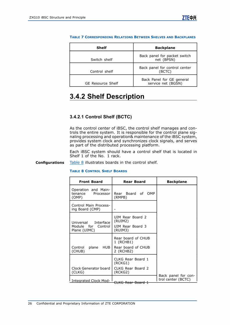
ZXG10 iBSC Structure and Principle
TABLE 7 CORRESPONDING RELATIONS BETWEEN SHELVES AND BACKPLANES
Shelf Backplane
Switch shelfBack panel for packet switch
net (BPSN)
Control shelfBack panel for control center
(BCTC)
GE Resource ShelfBack Panel for GE general
service net (BGSN)
3.4.2 Shelf Description
3.4.2.1 Control Shelf (BCTC)
As the control center of iBSC, the control shelf manages and con-trols the entire system. It is responsible for the control plane sig-naling processing and operation& maintenance of the iBSC system,provides system clock and synchronizes clock signals, and servesas part of the distributed processing platform.
Each iBSC system should have a control shelf that is located inShelf 1 of the No. 1 rack.
Configurations Table 8 illustrates boards in the control shelf.
TABLE 8 CONTROL SHELF BOARDS
Front Board Rear Board Backplane
Operation and Main-tenance Processor(OMP)
Rear Board of OMP(RMPB)
Control Main Process-ing Board (CMP) -
Universal InterfaceModule for ControlPlane (UIMC)
UIM Rear Board 2(RUIM2)
UIM Rear Board 3(RUIM3)
Control plane HUB(CHUB)
Rear board of CHUB1 (RCHB1)
Rear board of CHUB2 (RCHB2)
Clock Generator board(CLKG)
CLKG Rear Board 1(RCKG1)
CLKG Rear Board 2(RCKG2)
Integrated Clock Mod- CLKG Rear Board 1
Back panel for con-trol center (BCTC)
26 Confidential and Proprietary Information of ZTE CORPORATION

Chapter 3 Hardware Structure
Front Board Rear Board Backplane
ule (ICM)
(RCKG1)
CLKG Rear Board 2(RCKG2)
Server board (SBCX)Rear board of ServerBlade (RSVB)
Figure 6 illustrates the configurations of the control shelf.
FIGURE 6 CONTROL SHELF CONFIGURATIONS
The following describes boards in the control shelf.
1. Two OMP boards must be installed in Slots 11 and 12, whichwork in the active/standby mode.
2. Two to four CMP boards should be installed in Slots 1 through4 in the active/standby mode. The specific quantity is deter-mined based on system capacity.
Note:
If the capacity needs expansion, the CMP boards can beinstalled in other shelves (the packet switch shelf is recom-mended).
3. Two SBCX boards must be installed in Slots 5 and 7, whichwork in the active/standby mode.
4. Two CLKG/ICM boards must be installed in Slots 13 and 14,which work in the active/standby mode.
Confidential and Proprietary Information of ZTE CORPORATION 27

ZXG10 iBSC Structure and Principle
Note:
Use CLKG(ICM) board pairs or ICM board pairs. Differentboards cannot be used together.
5. Two CHUB boards must be installed in Slots 15 and 16, whichwork in the active/standby mode.
6. Two UIMC boards must be installed in Slots 9 and 10, whichwork in the active/standby mode.
7. One RUIM2 board must be installed in Slot 9.
8. One RUIM3 board must be installed in Slot 10.
9. Two RMPB boards must be installed in Slots 11 and 12.
10.One RCKG1 board should be installed in Slot 13.
11.One RCKG2 board should be installed in Slot 14.
12.One RCHB1 board should be installed in Slot 15.
13.One RCHB2 board should be installed in Slot 16.
14. Two RSVC boards should be installed in Slots 5 and 7.
15.One RBID board should be installed on the BCTC.
Principles Figure 7 illustrates the working principles of the control shelf.
FIGURE 7 CONTROL SHELF PRINCIPLES
1. Communication between shelves
28 Confidential and Proprietary Information of ZTE CORPORATION

Chapter 3 Hardware Structure
i. The iBSC system can be configured with one pair ofCLKG/ICM boards.The CLKG/ICM boards are usually in-stalled in the control subrack, and distributes systemclock signals to the packet switch network and the Gigabitresource shelf.
ii. The OMC2 network interface on the rear board of OMP isconnected to the OMP1 network interface on the rear boardof SBCX through the HUB; the OMC1 network interface onthe rear board of SBCX is connected to the external networkthrough another HUB to separate intranet segments andInternet segments. The OMM is installed on the SBCX.
iii. The CHUB acts as the control stream convergence centerfor the control streams from the switch shelf, the Gigabitresource shelf and the control shelf.
2. Intra-shelf communication
i. The BCTC backplane bears the signaling processing boardand main control modules. It is responsible for the conver-gence and processing of the control plane, and serves aspart of the distributed processing platform in a multi-shelfdevice.
ii. The UIMC board is the signaling exchange center of thecontrol subrack. It exchanges information between mod-ules.
iii. The OMP board implements the control related to the op-eration and maintenance of the entire system (includingoperation and maintenance agent).
As the processing core of iBSC operation & maintenance,the OMP board directly or indirect monitors and manages allboards in the system. It provides two links (Ethernet inter-face and RS485) for configuration management of systemboards.
iv. The SBCX serves as the OMM server. It also stores files forthe OMP and organizes these files according to the formatsrequired by the OMM.
v. The CMP board connects with the control plane switch unitand processes all protocols of the control plane.
Backplane The backplane of the control shelf if the BCTC board version060201. Figure 8 shows the back view of the BCTC.
Confidential and Proprietary Information of ZTE CORPORATION 29

ZXG10 iBSC Structure and Principle
FIGURE 8 BCTC BACK VIEW
1. Power Interfaces
Table 9 illustrates the power interfaces of the control shelf.
TABLE 9 POWER INTERFACES OF THE CONTROL SHELF
InterfaceID Purpose Connection Relations
X1, X2 Power socket
Through the subrack power filter,X1 and X2 parallel connect to the-48 V, -48 VGND and PE signalpole of rack bus bar.
2. Backplane DIP Switches
The DIP switches are located on the RBID, as shown in Figure9.
30 Confidential and Proprietary Information of ZTE CORPORATION
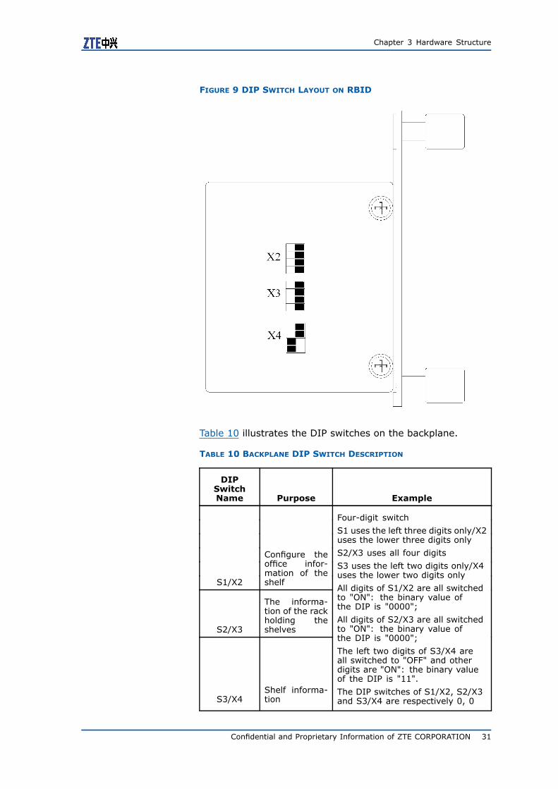
Chapter 3 Hardware Structure
FIGURE 9 DIP SWITCH LAYOUT ON RBID
Table 10 illustrates the DIP switches on the backplane.
TABLE 10 BACKPLANE DIP SWITCH DESCRIPTION
DIPSwitchName Purpose Example
S1/X2
Configure theoffice infor-mation of theshelf
S2/X3
The informa-tion of the rackholding theshelves
S3/X4Shelf informa-tion
Four-digit switch
S1 uses the left three digits only/X2uses the lower three digits only
S2/X3 uses all four digits
S3 uses the left two digits only/X4uses the lower two digits only
All digits of S1/X2 are all switchedto "ON": the binary value ofthe DIP is "0000";
All digits of S2/X3 are all switchedto "ON": the binary value ofthe DIP is "0000";
The left two digits of S3/X4 areall switched to "OFF" and otherdigits are "ON": the binary valueof the DIP is "11".
The DIP switches of S1/X2, S2/X3and S3/X4 are respectively 0, 0
Confidential and Proprietary Information of ZTE CORPORATION 31

ZXG10 iBSC Structure and Principle
DIPSwitchName Purpose Example
and 3. All the actual rack numbersshould add 1, so this configurationmeans: office 0, rack 1, shelf 4.
Note:
Backplanes BPSN, BCTC and BGSN all have DIP switches withthe same ON/OFF setting method.
OFF: move the switch downward, representing "1";
ON: move the switch upward, representing "0".
Jumpers may also be used to set shelf information of the site.In this case, one jumper path represents one digit. Threefour-path jumpers are available, which represent the office in-formation, rack information and shelf information. See Table10 for specific meanings of the jumpers.
OFF: plug off the short-circuited module, representing "1";
OFF: plug on the short-circuited module, representing "0".
3.4.2.2 Switch Shelf (BPSN)
The packet switch shelf provides the IP switching function for theuser plane data in each functional entity in the iBSC system, andprovides corresponding QoS functions for different users.
Each iBSC system must be configured with one packet switch shelfthat is installed on the fourth level of the active cabinet.
Configurations Table 11 illustrates boards that can be configured in the packetswitch shelf.
TABLE 11 BOARDS FOR THE PACKET SWITCH SHELF
Front Board Rear Board Backplane
Packet Switch Net-work (PSN) Board -
Gigabit line interfaceboard (GLI) -
Control Main Process-ing Board (CMP) -
Universal InterfaceModule for ControlPlane (UIMC)
UIM Rear Board 2(RUIM2)
UIM Rear Board 3(RUIM3)
Back panel for packetswitch net (BPSN)
Figure 10 illustrates the configurations of a packet switch shelf.
32 Confidential and Proprietary Information of ZTE CORPORATION

Chapter 3 Hardware Structure
FIGURE 10 PACKET SWITCH SHELF CONFIGURATIONS
1. The packet switch shelf provides a Level 1 IP switch platformfor the user plane expansion of multiple resource shelves. Itcan also directly provide external high-speed interfaces. Eachpair of GLI boards provide eight pairs of active/standby opticalinterfaces. Three pairs of GLI boards provide 24 pairs of opti-cal interfaces that connect with the 24 active/standby opticalinterfaces on the GUIM boards in the six-level resource shelf.Each GUIM board uses two pairs of optical interfaces.
2. Description of board configurations in the shelf
i. Two UIMC boards must be installed, which are responsiblefor the control plane switch of the packet switch shelf. Theywork in the active/standby mode and are inserted into Slots15 and 16.
ii. Two PSN boards must be installed, which are responsiblefor the data exchange between line cards. They work inthe load sharing mode and are inserted into Slots 7 and 8.
iii. Two to six GLI boards that serve as GE line cards. They canbe installed in Slots 1 through 6, and their quantity can bechosen according to capacity needs. However, they mustbe installed in pairs, and added from the left slot to theright to work in the load sharing mode.
iv. 0 to two CMP boards that work in the active/standby mode.One pair of CMP boards should be installed for every 1024carriers. They should be installed in Slots 11 through 14.
v. One RUIM2 board must be installed in Slot 15.
vi. One RUIM3 board must be installed in Slot 16.
vii. One RBID board must be installed on the BPSN.
Principles Figure 11 illustrates the working principles of the packet switchshelf when the Gigabit resource shelf is used.
Confidential and Proprietary Information of ZTE CORPORATION 33

ZXG10 iBSC Structure and Principle
FIGURE 11 PACKET SWITCH SHELF WORKING PRINCIPLES
1. Communication between shelves
i. The resource shelves are connected to the GLI boards inthe switch shelf through the optical interfaces on the frontpanel of the GUIM boards.
ii. The control shelf is connected to the UIMC board in theswitch shelf through RCHB1 and RCHB2, which are rearboards of CHUB.
iii. Clock signals re connected to the UIMC board in the switchshelf to implement signal transmission through RCKG1 andRCKG2, which are rear boards of the CLKG/ICM board.
2. Intra-shelf communication
i. User plane data
– The packet switch shelf processes user plane data re-ceived through the GLI board.
– The data is then sent to the PSN to be switched throughthe high-speed signal cables on the backplane.
– At last, the GLI board receives data from the PSN, pro-cesses the data and then sends to the target port.
ii. Control plane data
The UIMC switch is the process to use the Ethernet bus asthe internal control bus of the subsystem, which connectsto various modules in the subsystem to distribute and col-lect information, manage system configuration and main-tenance, and meanwhile implements higher-layer protocolsand transmits signaling data.
Backplane The backplane of the packet switch network is BPSN version070200. Figure 12 shows the backview of the BPSN.
34 Confidential and Proprietary Information of ZTE CORPORATION

Chapter 3 Hardware Structure
FIGURE 12 BPSN BACK VIEW
1. Backplane Interfaces
Table 12 illustrates the power supply interfaces of the packetswitch shelf.
TABLE 12 POWER SUPPLY INTERFACES IN PACKET SWITCH SHELF
InterfaceID Purpose Connection Relations
X1, X2, X3Powersocket
Through the subrack power filter, X1,X2 and X3 parallel connect to the -48V, -48 VGND and PE signal pole of rackbus bar.
2. Backplane DIP Switch
The DIP switches on the BPSN are located on the RBID (X2,X3 and X4). They are used to set the office, rack and rackof the shelf. For setting methods, see "Backplane DIP SwitchDescription".
3.4.2.3 Gigabit Resource Shelf (BGSN)
As the universal service shelf, the Gigabit resource shelf supportsmultiple service processing modules to form various universal ser-
Confidential and Proprietary Information of ZTE CORPORATION 35

ZXG10 iBSC Structure and Principle
vice processing subsystems. It can be installed with the Abis in-terface unit, A interface unit, PCU (GIU), TC unit and Ater interfaceunit.
There is no special restriction on its location. It is usually locatedin Level 1 and Level 3 of No. 1 rack and any level in No. 2 rack.
Configurations Table 13 describes boards that can be configured in the Gigabitresource shelf.
TABLE 13 GIGABIT RESOURCE SHELF BOARDS
Front Board Rear Board Backplane
Digital Trunk Board(DTB)
Digital Trunk RearBoard (RDTB)
Sonet Digital TrunkBoard(SDTB2)
General Rear InterfaceModule 1 (RGIM1)
Gigabit UniversalInterface Module(GUIM)
Rear board of GUIM 1(RGUIM1), Rear boardof GUIM 2 (RGUIM2)
GSM UniversalProcessing board(GUP2) -
Single port GE LineInterface Board(GIPI)
Resource shelf GE Rearcard (RGER)
MNIC Rear Board(RMNIC)
Signaling ProcessingBoard (SPB2)
Rear Board of SPB2(RSPB)
E1 IP interfaceboard (EIPI) -
Operation and Main-tance Processor(OMP)
Rear Board of OMP(RMPB)
Control Main Pro-cessing Board (CMP) -
Back Panel for GE gen-eral service net (BGSN)
Multiple configuration methods can be applied to the Gigabit re-source shelf. The following is a configuration wherein E1 or IPoE isadopted for the Abis interface, and E1 is adopted for the A inter-face and the Gb interface.Figure 13 illustrates the configurationsof a Gigabit resource shelf.
36 Confidential and Proprietary Information of ZTE CORPORATION

Chapter 3 Hardware Structure
FIGURE 13 GIGABIT RESOURCE SHELF CONFIGURATION
The following describes boards in the Gigabit resource shelf.
1. Two GUIM boards must be installed in Slots 9 and 10, whichwork in the active/standby mode. The GUIM boards connectto the Level 1 switch through multiple-mode optical cables.
2. The DTB can be installed in Slots 9, 10, 15 or 16. The numberof consecutive DTBs should not exceed three. Slots 1 and 17may cause wiring difficulties, so they should be avoided wheninstalling the DTBs. Each shelf should configure six DTBs (themaximum allowed DTBs is eight).
3. The SDTB2 board can be installed in Slots 9, 10 or 17, whichwork in the active/standby mode. Two pairs of single-modeoptical cables can be led out of the SDTB2 panel. If the STDB2boards are not configured in the active/standby mode, whenthey are installed in the active and standby slots, their adjacentactive and standby slots cannot use boards that utilize the HWlines, such as DTB, GUP2, SPT2 and EIPI.
4. The GUP2 board can be installed in Slots 9, 10, 1 or 17.
5. SPB2 can be inserted into any slot except slots 9 and 10, butonly one SPB can be inserted into slot 15 or 16.
6. The GIPI boards can be inserted into any slot except slots 9 and10, but only one GIPI board can be inserted into slot 15 or 16.The GIPI panel has one Gigabit optical interface, or the RGERcan be configured to provide one Gigabit electrical interface,or the RMINC can be configured to provide four FE electricalinterfaces that work in the active/standby mode.
When GIPI board provides OMCB channels or connects with theMR server, it can be inserted in Slots 5 through 8 and Slots 13and 14, and work in the active/standby mode. In this case, theGIPI board uses RMNIC as its rear board and provides eight FEinterfaces, four for internal connection and four for externalconnection.
Confidential and Proprietary Information of ZTE CORPORATION 37

ZXG10 iBSC Structure and Principle
7. The EIPI boards can be inserted into any slot except slots 9and 10, but only one EIPI board can be inserted into slot 15 or16.
8. If an office contains one shelf or two shelves, the OMP boardsmust be installed in Slots 11 and 12, and the CMP boards maybe installed in Slots 11 through 14 as required.
9. If SDTB2, SPB2, GIPI, EIPI or GUP2 boards are installed inSlots 15 or 16, then the TDM board cannot extract line 8 Kclock reference and the serial port in Slot 16 cannot be used.
10.One RGUM1 and one RGUM2 board must be installed in Slots9 and 10.
11.RDTB, RSPB and RGER/RMNIC boards must be installed if theirfront boards are installed.
12. The rear board of the SDTB2 board, namely RGIM1, extractsthe 8 K clock of the STM-1 line, so it is not needed if line clockextraction is not necessary. If the system has more than oneSDTB2 board, two RGIM1 boards should be installed, and twoclock extraction lines should be connected.
13.One RBID board must be installed on the BGSN.
Principles Figure 14 illustrates the working principles of the Gigabit switchresource shelf.
FIGURE 14 GIGABIT RESOURCE SHELF PRINCIPLES
1. Communication between shelves
i. The GUIM board provides the control Ethernet channel thatconnects to the CHUB boards in the control stream conver-gence center of the control shelf.
The GUIM board interconnects with the GLI board in theBPSN to carry out level 1 switch between different resourceboards.
ii. DTB and SPB2 boards provide E1 interfaces.
iii. The SDTB2 board provides STM-1 access.
iv. The GIPI board provides GE access.
38 Confidential and Proprietary Information of ZTE CORPORATION

Chapter 3 Hardware Structure
v. The EIPI board provides E1/T1 based IP access, which iscompleted with aid from the DTB or the SDTB2 board.
vi. The CLKG/ICM board in the control shelf distributes systemclock signals to Gigabit resource shelves.
2. Intra-shelf communication
i. As the backplane of the Gigabit resource shelf, the BGSNsupports multiple service processing modules to form var-ious universal service processing subsystems.
ii. The GUIM board is the convergence and switch center forvarious data in the BGSN. It completes the information ex-change between modules.
iii. The GUP2 board processes user plane related radio proto-cols, TC code conversion and rate adaptation, and conver-sion from TDM to IP packets.
iv. The GIPI board provides one Gigabit electrical interface orfour FE interfaces to the internal media plane through thebackplane.
Backplane The backplane of the Gigabit resource shelf is BGSN. Figure 15shows the back view of the BGSN.
FIGURE 15 BPSN BACK VIEW
1. Backplane Interfaces
Table 14 illustrates the power interfaces of the Gigabit resourceshelf.
Confidential and Proprietary Information of ZTE CORPORATION 39

ZXG10 iBSC Structure and Principle
TABLE 14 POWER INTERFACES OF THE GIGABIT RESOURCE SHELF
Interface ID Purpose Connection Relations
X1, X2, X3 Power socket
Through the subrack power filter,X1, X2 and X3 parallel connectto the -48 V, -48 VGND and PEsignal pole of rack bus bar.
2. Backplane DIP Switches
The DIP switches on the BGSN are located on the RBID (X2,X3 and X4). They are used to set the office, rack and rackof the shelf. For setting methods, see "Backplane DIP SwitchDescription".
3.4.3 Inter-Shelf Connections
Internal cables of iBSC are used for signal interconnection betweeninternal boards of the system.
Internal cable connections for the resource shelf (BUSN) and theGE resource shelf are different, which will be discussed in the fol-lowing.
3.4.3.1 Internal Connections
One Cabinet 1. For the configuration of one cabinet, internal cables in the iBSCsystem include:
i. Clock distribution cable and line clock extraction cable;
ii. Control-plane Ethernet cable;
iii. User-plane optical fiber;
iv. Monitoring cable.
2. Connection Case Description
i. Clock Extraction and Distribution
Figure 16 illustrates the clock extraction and distributionconnections for a single cabinet of iBSC.
40 Confidential and Proprietary Information of ZTE CORPORATION

Chapter 3 Hardware Structure
FIGURE 16 CLOCK EXTRACTION AND DISTRIBUTION FOR IBSCWITH A SINGLE CABINET
Note:
In Figure 16, CLKG(ICM) board can be replaced with ICM;both CLKG(ICM) and ICM can provide clock signals. Thisapplies to other parts of this section.The DTB, STDB, SDTB2and SPB2 can all extract clock signals for the CLKG(ICM) orthe ICM. The figure shows only the DTB.
The clock extraction method is as follows:
– Clock reference for clock extraction
Extracts the CN line clock from the interface board, andthen sends it to the CLKG(ICM)/ICM board.
The CLKG(ICM)/ICM board can also input BITS clockreference or obtain clock reference from the GPS mod-ule.
– Clock Distribution
Clock signals are transmitted to the GUIM/UIMC boardsin the shelves from RCKG1 and RCKG2 boards throughthe clock cables, and then distributed to slots in thelocal shelf through the GUIM/UIMC boards.
ii. Control plane Ethernet interconnection
Figure 17 illustrates the Ethernet interconnection of thecontrol plane.
Confidential and Proprietary Information of ZTE CORPORATION 41

ZXG10 iBSC Structure and Principle
FIGURE 17 CONTROL PLANE ETHERNET INTERCONNECTION FORIBSC WITH ONE CABINET
In Figure 17, solid lines represent cable connections whiledotted lines represent connections using the printed lineson the backplane.
The Ethernet interconnection for the control plane of theiBSC system is implemented by the CHUB board. Inter-connection modes are as follows:
– Connect the GUIM in the Gigabit resource shelf or theUIMC in the packet switch shelf with the CHUB throughcables.
– Connect the UIMC in the control shelf with the CHUBdirectly through printed lines on the backplane.
iii. User plane interconnection
Figure 18 illustrates the user plane connection of iBSC withone cabinet.
FIGURE 18 USER PLANE CONNECTION OF IBSC WITH ONE CABINET
42 Confidential and Proprietary Information of ZTE CORPORATION

Chapter 3 Hardware Structure
The user planes in the same Gigabit resource shelf are in-terconnected through the backplane; User planes in dif-ferent Gigabit resource shelves are interconnected throughthe GLI and PSN boards in the packets switch shelves, thatis, through cables that connect the GUIM boards in the Gi-gabit resource shelves with the GLI boards.
iv. Connection of the Monitoring Cables
Figure 19 illustrates the monitoring cable connection ofiBSC with one cabinet.
FIGURE 19 MONITORING CABLE CONNECTION OF IBSC WITH ONECABINET
The fan subracks and power distribution subracks are con-nected with cables in order to monitor the fans.
The OMP board is connected with the PWRD board in thepower distribution subrack in order to monitor the PWRDboard.
Sensors are connected to the power distribution subrack inorder to monitor the peripheral environment.
Dual Cabinets 1. For the configuration of dual cabinets, the cables between iBSCcabinets include the following:
i. Clock distribution cable and line clock extraction cable;
ii. Control-plane Ethernet cable;
iii. User-plane optical fiber;
iv. Monitoring cable.
2. Connection Case Description
i. Clock Distribution
Figure 20 illustrates the clock extraction and distributionconnections for iBSC with dual cabinets.
Confidential and Proprietary Information of ZTE CORPORATION 43

ZXG10 iBSC Structure and Principle
FIGURE 20 CLOCK EXTRACTION AND DISTRIBUTION FOR IBSCWITH DUAL CABINETS
Each shelf in iBSC needs the system clock. The clock ex-traction method is as follows:
– Clock reference for clock extraction
Extracts the CN line clock from the interface board, andthen sends it to the CLKG(ICM)/ICM board.
The CLKG(ICM)/ICM board can also input BITS clockreference or obtain clock reference from the GPS mod-ule.
– Clock Distribution
Clock signals are transmitted to the GUIM boards inthe Gigabit resource shelves or the UIMC boards in thepacket switch shelves from RCKG1 and RCKG2 boardsthrough the clock cables, and then distributed to slotsin the local shelf through the GUIM or UIMC boards.
ii. Control plane Ethernet interconnection
Figure 21 illustrates the control plane Ethernet intercon-nection for iBSC with dual cabinets.
44 Confidential and Proprietary Information of ZTE CORPORATION

Chapter 3 Hardware Structure
FIGURE 21 CONTROL PLANE ETHERNET INTERCONNECTION FORIBSC WITH DUAL CABINETS
In Figure 21, solid lines represent cable connections whiledotted lines represent connections using the printed lineson the backplane.
The control plane Ethernet interconnection modes for iBSCwith dual cabinets are as follows:
– Connect the UIMC or GUIM boards in all the shelves(except for the control shelf) in No. 1 rack with theCHUB board.
– Connect the UIMC board in the control shelf of No. 1rack with the CHUB directly through printed lines on thebackplane.
iii. User plane interconnection
Figure 22 illustrates the user plane interconnection for iBSCwith dual cabinets.
FIGURE 22 USER PLANE CONNECTION OF IBSC WITH DUALCABINETS
Confidential and Proprietary Information of ZTE CORPORATION 45

ZXG10 iBSC Structure and Principle
The user planes in the same Gigabit resource shelf are in-terconnected through the backplane; User planes in dif-ferent Gigabit resource shelves are interconnected throughthe GLI and PSN boards in the packets switch shelves, thatis, through cables that connect the GUIM boards in the Gi-gabit resource shelves with the GLI boards.
iv. Connection of the Monitoring Cables
Figure 23 illustrates the monitoring cable connection ofiBSC with dual cabinets.
FIGURE 23 MONITORING CABLE CONNECTION OF IBSC WITH DUALCABINETS
The fan subracks and power distribution subracks in eachcabinet are connected with cables in order to monitor thefans.
In No. 1 rack, the OMP board is connected with the PWRDboard; In No. 2 rack, the PWRD board is connected to thePWRD board in the No. 1 rack. Thus, the PWRD boards inboth cabinets can be monitored.
Sensors are connected to the power distribution subrack inNo. 1 rack in order to monitor the peripheral environment.
46 Confidential and Proprietary Information of ZTE CORPORATION

Chapter4 Software Structure
After you have completed this chapter, you will know:
>> Front-End Software>> Background Software
4.1 Front-End SoftwareFigure 24 illustrates the front-end software structure of iBSC.
FIGURE 24 IBSC FRONT-END SOFTWARE STRUCTURE
The front-end software of iBSC includes the following:
1. BSP&Drivers
The BSP subsystem performs hardware drive of the entire sys-tem.It shields hardware operation details from the upper-layersoftware modules, abstracts hardware functions, and providesthe logical functions of the hardware devices to other softwaremodules only.
2. Operation Support Subsystem (OSS)
The OSS works above the BSP subsystem and below all othersubsystems. It shields all device drive interfaces from user
Confidential and Proprietary Information of ZTE CORPORATION 47

ZXG10 iBSC Structure and Principle
processes. It is responsible for process communication, filemanagement, device drive and process invocation.
3. Bearer Subsystem (BRS)
The bearer subsystem provides IP and TDM bearer servicesto the Service Support Subsystem, the Signaling Subsystemand the OMS. Its functions include link layer functions, net-work transmission, dynamic routing, ATM processing and traf-fic control.
4. PP Subsystem
The PP Subsystem implements the following functions: man-agement of the digital trunk interface, connection of switchingnetworks, provision of system clocks and corresponding man-agement, environment control and power management.
5. System Control Subsystem (SCS)
The System Control Subsystem works above the OSS and theDatabase Subsystem. It is responsible for the monitoring, startand version download of the entire system.
6. Database Subsystem
The DBS works above the OSS. It is responsible for NE physicalresource management and the configuration management ofservices, signaling and protocols. It also provides databaseaccess interfaces to other subsystems.
7. Operation and Maintenance Subsystem (OMS)
Provides performance management, fault management, secu-rity management, signaling tracing, and dynamic data obser-vation functions. It implements the functions of the Operationand Management System on the foreground.
8. Signaling Subsystem (SS)
The Signaling Subsystem works above the OSS, the DBS andthe BRS. It implements narrowband and broadband SS7 sig-naling, call signaling, IP signaling and gateway control signal-ing, and provides services to the RAN Control Plane Subsystem(RANC) and the RAN Service Support Subsystem (RANSS).
9. RAN Control Plane Subsystem (RANC)
The RAN Control Plane Subsystem processes the Level 3control plane protocols and controls call signaling connec-tion, including radio resource management, dynamic channelresource adjustment, load control, access control, handoverdecision and signaling connection management.
10.RAN User Plane Subsystem (RANU)
For PS services, the RAN User Plane Subsystem is responsiblefor mutual data forwarding and scheduling between the radioand Gb interfaces according to QoS requirements.For CS ser-vices, the RAN User Plane Subsystem provides the TC functionon the GUP board.
11.RAN Service Support Subsystem (RANSS)
It provides support for the control plane subsystem and theuser plane subsystem. It provides assurance for the smoothongoing of services, provides monitoring methods for variousservices and, and completes the global flow processing of iBSC.
48 Confidential and Proprietary Information of ZTE CORPORATION

Chapter 4 Software Structure
Its functions include signaling tracing, load control, access con-trol, performance measurement and global flow processing.
12.Micro-Code Subsystem (MCS)
The MCS implements quick processing of user plane data andseparates the control plane from the data plane.
4.2 Background SoftwareThe background software, NetNumen(TM) M31, runs on the OMMserver and the client and communicates with the iBSC using theTCP/IP protocols. Functions of NetNumen(TM) M31 include thefollowing:
1. Configuration Management
2. Fault Management
3. Performance Management
4. System Management
5. Log Management
6. Version Management
7. Topology Management
8. Security Management
Confidential and Proprietary Information of ZTE CORPORATION 49

ZXG10 iBSC Structure and Principle
This page is intentionally blank.
50 Confidential and Proprietary Information of ZTE CORPORATION

Chapter5 System Principle
After you have completed this chapter, you will know:
>> Logical Units>> Clock Distribution>> User Plane Signaling Flow>> Control Plan Signaling Flow
5.1 Logical UnitsFigure 25 shows the hardware structure of iBSC.
FIGURE 25 HARDWARE SYSTEM STRUCTURE
Logically, the iBSC system is composed of six units.
1. Access Unit
The access unit provides the iBSC system with the access pro-cessing function of the A-interface, Alter interface, Abis inter-face and Gb interface. Access units of the iBSC system includethe A-Interface Unit (AIU) (when external TC is used, the AIUbelongs to the iTC system; iBSC adds the NSMU to the Aterinterface unit between it and the the iTC), the Abis InterfaceUnit (BIU) and the Gb Interface Unit (GIU).
2. The switching unit provides a large-capacity and non-blockingswitching platform for the system.
3. The CMPU processes upper-layer protocols of the control plane.
4. The UPU processes user plane protocols in the PS field.
Confidential and Proprietary Information of ZTE CORPORATION 51
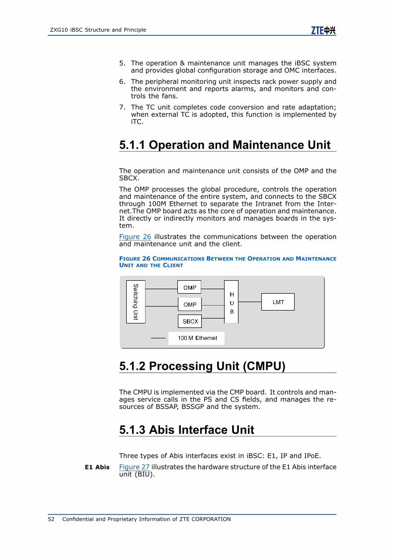
ZXG10 iBSC Structure and Principle
5. The operation & maintenance unit manages the iBSC systemand provides global configuration storage and OMC interfaces.
6. The peripheral monitoring unit inspects rack power supply andthe environment and reports alarms, and monitors and con-trols the fans.
7. The TC unit completes code conversion and rate adaptation;when external TC is adopted, this function is implemented byiTC.
5.1.1 Operation and Maintenance Unit
The operation and maintenance unit consists of the OMP and theSBCX.
The OMP processes the global procedure, controls the operationand maintenance of the entire system, and connects to the SBCXthrough 100M Ethernet to separate the Intranet from the Inter-net.The OMP board acts as the core of operation and maintenance.It directly or indirectly monitors and manages boards in the sys-tem.
Figure 26 illustrates the communications between the operationand maintenance unit and the client.
FIGURE 26 COMMUNICATIONS BETWEEN THE OPERATION AND MAINTENANCEUNIT AND THE CLIENT
5.1.2 Processing Unit (CMPU)
The CMPU is implemented via the CMP board. It controls and man-ages service calls in the PS and CS fields, and manages the re-sources of BSSAP, BSSGP and the system.
5.1.3 Abis Interface Unit
Three types of Abis interfaces exist in iBSC: E1, IP and IPoE.
E1 Abis Figure 27 illustrates the hardware structure of the E1 Abis interfaceunit (BIU).
52 Confidential and Proprietary Information of ZTE CORPORATION

Chapter 5 System Principle
FIGURE 27 E1 ABIS-INTERFACE UNIT HARDWARE STRUCTURE
The E1 Abis-interface unit consists of the DTB, the GUP and theSPB.
1. The DTB completes E1 access.
2. LAPD signaling from the BTS is switched to the SPB throughthe GUIM board in the local resource shelf. The SPB processesLAPD signaling.
3. CS and PS services are switched to the GUP board through theGUIM board in the local resource shelf. The GUP board finds20ms TRU frames or PCU frames according to channel search,and forms these frames into IP packets that are sent to theTCU or UPU for processing.
IP Abis Figure 28 illustrates the hardware structure of the IP Abis-interfaceunit.
FIGURE 28 IP ABIS INTERFACE HARDWARE STRUCTURE
Confidential and Proprietary Information of ZTE CORPORATION 53

ZXG10 iBSC Structure and Principle
The IP Abis interface unit is composed of the GIPI board and theGUP board.
1. As the interface board, the GIPI board receives IP packets fromthe BTS through the external Ethernet interface, and differen-tiates user plane data from control plane data.
� UDP data is sent through the user plane switch network tothe GUP for processing.
� SCTP data is sent through the control plane switch networkto the CMP for processing.
2. On the uplink direction, the GUP divides the IP packet payloadthat are composed based on carriers according to the channel,and searches the 20ms TRU frames or PCU frames in eachchannel. It then forms these frames into IP packets that aresent to the TCU(UPU) for processing. The downlink direction isjust opposite.
IPoE Abis Figure 29 illustrates the hardware structure of the IPoE Abis inter-face unit.
FIGURE 29 IPOE ABIS-INTERFACE UNIT HARDWARE STRUCTURE
1. The DTB completes E1 access.
2. The EIPI implements the conversion between PPP packets andIP packets, and differentiates user plane data from controlplane data.
� UDP data is sent through the user plane switch network tothe GUP for processing.
� SCTP data is sent through the control plane switch networkto the CMP for processing.
3. On the uplink direction, the GUP divides the IP packet payloadthat are composed based on carriers according to the channel,and searches the 20ms TRU frames or PCU frames in eachchannel. It then forms these frames into IP packets that are
54 Confidential and Proprietary Information of ZTE CORPORATION

Chapter 5 System Principle
sent to the TCU(UPU) for processing. The downlink direction isjust opposite.
5.1.4 A-Interface Uits
Two types of A-interfaces exist in iBSC: E1 and IP.
E1 A Figure 30 illustrates the hardware structure of the E1 A-interfaceunit.
FIGURE 30 E1 A-INTERFACE UNIT HARDWARE STRUCTURE
The E1 A-interface unit consists of DTBs (or SDTBs) and SPBs.
1. Packets from the PCM voice channel are received through theE1 A interface on the DTB/SDTB and SPB, and then switchedto the TCU through the GUIM of the local resource shelf.
2. In principle, SS7 timeslots are received through the E1 A in-terface on the SPB. The CPU on the CPU completes MTP2 pro-cessing and then forms IP packets that are sent to the COMPthrough the control plane switching network.SS7 timeslots canalso be received through the DTB/SDTB of the local shelf, andthen switched to the SPB through the GUIM of the local re-source shelf.
IP A Figure 31 illustrates the hardware structure of the IP A-interfaceunit.
Confidential and Proprietary Information of ZTE CORPORATION 55

ZXG10 iBSC Structure and Principle
FIGURE 31 IP A-INTERFACE UNIT HARDWARE STRUCTURE
The IP A interface unit is composed of GIPI boards and GUP boards.
1. The GIPI board completes IP access, and separates user planedata from control plane data.
� UDP data is sent through the user plane switch network tothe GUP for processing.
� SCTP data is sent through the control plane switch networkto the CMP for processing.
2. The GUP processes RTP and sends the processing result to theBIU through the GUIM.
5.1.5 Packet Control Unit
The Packet Control Unit (PCU) includes two logical units: GIU andUPU.
5.1.5.1 Gb Interface Unit
Two types of Gb interfaces exist in iBSC: E1 and IP.
56 Confidential and Proprietary Information of ZTE CORPORATION

Chapter 5 System Principle
E1 Gb Figure 32 illustrates the hardware structure of the E1 Gb interfaceunit.
FIGURE 32 E1 GB INTERFACE HARDWARE STRUCTURE
The E1 Gb interface unit consists of SPBs.
The SPB completes E1 access, processes FR protocol, and sepa-rates the user plane from the control plane for some data. It sendsuser plane data through the user plane switch network to the GUPfor processing, and sends control plane data through the controlplane switch network to the CMP for processing.
IP Gb Figure 33 illustrates the hardware structure of the IP Gb interfaceunit.
Confidential and Proprietary Information of ZTE CORPORATION 57

ZXG10 iBSC Structure and Principle
FIGURE 33 IB GB INTERFACE HARDWARE STRUCTURE
The IP Gb interface unit consists of CIPI boards. The GIPI boardcompletes IP access, and separates user plane data from controlplane data.
� UDP data is sent through the user plane switch network to theGUP for processing.
� For SCTP data, some is sent through the control plane switchnetwork to the CMP for processing, and some is sent throughthe user plane switch network to the GUP for processing.
5.1.5.2 Processing Unit
The Processing Unit (UPU) consists of UPPB2 boards. Its functionsinclude:
1. RLC/MAC Protocol processing
2. Partial BSSGP processing
3. Paging
4. Frame number synchronization
58 Confidential and Proprietary Information of ZTE CORPORATION

Chapter 5 System Principle
5.1.6 TransCoder Unit
The TransCoder Unit consists of GUP2(DRTB2) boards to imple-ment code transformation and rate adaptation.
5.1.7 IP Switch Unit
The IP Switch Unit (PSU) provides a large-capacity and unblockedIP switch network for system control management, communicationbetween service processing boards and traffic between multipleaccess units.The PSU consists of two levels of switch subsystems.
The Level 1 Switch Subsystem consists of PSN and GLI boardsthat provide management, core switch network board and line cardfunctions.
The Level 2 Switch Subsystem consists of UIMC, GUIM and CHUBboards, and is responsible for the exchange and convergence ofuser plane and control plane data flow in the system.
5.2 Clock DistributionThe system clock module of iBSC is on the CLKG/ICM board. TheCLKG board adopts the active/standby design, with the active andstandby boards locked to the same reference. The active andstandby clocks are directly connected using high impedance at theoutput drive end to realize smooth switchover.
Figure 34 illustrates the clock signal flow of the system.
Confidential and Proprietary Information of ZTE CORPORATION 59

ZXG10 iBSC Structure and Principle
FIGURE 34 SYSTEM CLOCK SIGNAL FLOW DIRECTION
The flow direction is described as follows:
1. The CLKG board is responsible for supplying clock signals andexternal synchronization functions. It extracts clock referencevia the A-interface and drives multiple channels of clock ref-erence signals for use by the resource shelf and the packetswitch shelf after intra-board synchronization.
2. The clock signals are driven by the UIMC or GUIM to slots inthe local shelf through the backplane.
5.3 User Plane Signaling Flow
5.3.1 User Plane Signal Flow in the CSDomain
Signal FlowObserved fromLogical Units
Figure 35 illustrates the control plane signal flow in the CS Domainobserved from the logical units.
60 Confidential and Proprietary Information of ZTE CORPORATION

Chapter 5 System Principle
FIGURE 35 CONTROL PLANE SIGNAL FLOW IN THE CS DOMAIN (LOGICALUNITS)
The figure above shows the uplink signal flow, which is contrary tothe downlink signal flow.
The BIU severs user plane data from control plane data, and thensends user plane data to the TCU, which processes such data andthen sends it to the AIU. Signal flow: 1®2.
Signal FlowObserved from
Shelves
Figure 36 illustrates the user plane signal flow in the CS Domainobserved from the shelves.
FIGURE 36 USER PLANE SIGNAL FLOW IN THE CS DOMAIN (SHELVES)
Confidential and Proprietary Information of ZTE CORPORATION 61

ZXG10 iBSC Structure and Principle
5.3.2 User Plane Signal Flow in the PSDomain
Signal FlowObserved fromLogical Units
Figure 37 illustrates the control plane signal flow in the PS Domainobserved from the logical units.
FIGURE 37 CONTROL PLANE SIGNAL FLOW IN THE PS DOMAIN (LOGICALUNITS)
The figure above shows the uplink signal flow, which is contrary tothe downlink signal flow.
The BIU severs CPU frames from all frames and sends them to theUPU(UPPB) through the user plane switching network. The UPUthen separates PS Domain user plane data from CPU frames re-ceived for further processing. After data processing is complete,the data is sent to the GUI through the user plane switching net-work.Signal flow: 1®2.
62 Confidential and Proprietary Information of ZTE CORPORATION

Chapter 5 System Principle
Signal FlowObserved from
Shelves
Figure 38 illustrates the user plane signal flow in the PS Domainobserved from the shelves.
FIGURE 38 USER PLANE SIGNAL FLOW IN THE PS DOMAIN (SHELVES)
5.4 Control Plan Signaling Flow
5.4.1 Control Plane Signal Flow in theCS Domain
Signal FlowObserved fromLogical Units
Figure 39 illustrates the control plane signal flow in the CS Domainobserved from the logical units.
FIGURE 39 CONTROL PLANE SIGNAL FLOW IN THE CS DOMAIN (LOGICALUNITS)
Confidential and Proprietary Information of ZTE CORPORATION 63

ZXG10 iBSC Structure and Principle
Abis-interface signaling flow: Abis interface unit (BIU) sends sig-naling in the LAPD channel to the CMP board as control plane data.The CMP processes such data and sends some of it directly backto the BIU (flow direction: 1®1). Some signaling data will be sentto the AIU in the form of A-interface signaling flow (flow direction:1®2).
A-interface signaling flow: The AIU processes the MTP2 part ofA-interface signaling, and then sends it to the CMP to complete theprocessing of MTP3 and layers above. Some global processes needthe participation of the OMP. Its data flow direction is: 2®3®3®2or 2®2.
Signal FlowObserved from
Shelves
Figure 40 illustrates the control plane signal flow in the CS Domainobserved from the shelves.
FIGURE 40 CONTROL PLANE SIGNAL FLOW IN THE CS DOMAIN (SHELVES)
64 Confidential and Proprietary Information of ZTE CORPORATION

Chapter 5 System Principle
5.4.2 Control Plane Signal Flow in thePS Domain
Signal FlowObserved fromLogical Units
Figure 41 illustrates the control plane signal flow in the PS domainobserved from the logical units.
FIGURE 41 CONTROL PLANE SIGNAL FLOW IN THE PS DOMAIN (LOGICALUNITS)
1. Abis-interface signaling flow
i. The Abis interface unit (BIU) sends control plane data in theLAPD channel to the CMP board. The CMP processes suchdata and sends some of it directly back to the BIU (flowdirection: 1®1). Some data, such as packet assignmentmessages, is sent to the UPU (UPPB), which processes thedata and then sends it to the BIU through the user planeswitch network (flow direction: 1®3®2).
ii. Data from the Abis interface unit is sent to the UPU throughthe user plane switch network. The UPU processes the dataand separates control signaling packets, which are sent tothe control plane processing board (CMP). Its data flow di-rection is: 2®3®3®2.
2. The signaling flow of the Gb interface is described as follows:
i. The GIU sends BVC channel data as control plane data tothe active CMP. The CMP processes the data and sendssome of it (such as PTP BVC restart) to other CMPs andsome (sch as signaling BVC restart) to the OMP. The CMPor the OMP processes the data and some signaling gener-ates the Abis signaling traffic, such as paging messages inthe PS or CS domain, whose data flow is 5®1 or 5®3®2;other signaling, such as PTP BVC restart acknowledgementand signaling BVC restart acknowledgement, is sent to theGb interface through the GUI, with the data flow as 5®5 or6®6.
ii. The GUI routes data from other BVC channels to the userplane processing unit, which separates control plane dataand sends it to the CMP. The CMP processes the data andsome signaling, such as PTP paging messages, is sent to
Confidential and Proprietary Information of ZTE CORPORATION 65

ZXG10 iBSC Structure and Principle
the Gb interface through the GIU with the data flow as4®3®5; some signaling generates the Abis signaling flow,such as location messages, with the data flow as 4®3®1.
Signal FlowObserved from
Shelves
Figure 42 illustrates the control plane signal flow (1®3®2) in thePS domain observed from the shelves.
FIGURE 42 CONTROL PLANE SIGNAL FLOW (1®®®3®®®2) IN THE PS DOMAIN(SHELVES)
Figure 43 illustrates the control plane signal flow (5®3®2) in thePS domain observed from the shelves.
66 Confidential and Proprietary Information of ZTE CORPORATION

Chapter 5 System Principle
FIGURE 43 CONTROL PLANE SIGNAL FLOW (5®®®3®®®2) IN THE PS DOMAIN(SHELVES)
Confidential and Proprietary Information of ZTE CORPORATION 67

ZXG10 iBSC Structure and Principle
This page is intentionally blank.
68 Confidential and Proprietary Information of ZTE CORPORATION

Chapter6 Interface and Protocol
After you have completed this chapter, you will know:
>> Interfaces>> Protocols
6.1 Interfaces
6.1.1 A-Interface
The interface between BSC and MSC is called A-interface. Moreaccurately, A-interface is the interface between TC and MSC.
Transcoder implements the voice transformation between voicecoding and 64 kbps A law PCM coding. At the same time, it per-forms the data rate adaptation in the circuit data service. TC canbe either at BSC side or MSC side
The A-interface of iBSC supports three kinds of interfaces.
1. E1 interface
In this case, iBSC is connected with MSC by 75 Ω coaxial cableor 120 Ω twisted pair.
At A-interface, the data link layer employs MTP2 protocol, thenetwork layer employs MTP3 protocol and SCCP protocol, andthe application layer employs BSSMAP protocol.
2. STM-1 interface
In this case, iBSC is connected with MSC by optical fiber.
3. IP interface
In this case, iBSC is connected with MSC by network cable.
6.1.2 Ater Interface (TC Is External)
The interface between iBSC and iTC is called Ater interface.TransCoder (TC) is separated from iBSC and exists as an indepen-dent system iTC, which facilitates dynamic TC resource sharing.For more details, refer to ZXG10 iTC Transcoder Pool SystemDescription.
The Ater interface of iBSC supports two kinds of interfaces.
1. E1 interface
In this case, iBSC is connected with iTC by 75 Ω coaxial cableor 120 Ω twisted pair.
Confidential and Proprietary Information of ZTE CORPORATION 69

ZXG10 iBSC Structure and Principle
At Ater interface, the data link layer employs MTP2 protocol,the network layer employs MTP3 protocol and SCCP protocol,and the application layer employs Ater interface applicationlayer protocol.
2. STM-1 interface
In this case, iBSC is connected with iTC by optical fiber.
6.1.3 Abis Interface
The interface between BSC and BTS is called Abis interface. BSCis connected with BTS via Abis interface. Abis interface is the in-ternal user-defined interface of ZXG10 BSS. When E1 is used fortransmission, Abis interface supports various networking modes,such as star networking, chain networking, tree networking, andring networking.
The Abis interface of iBSC supports four kinds of interfaces.
1. E1/T1 interface
If Abis interface adopts E1 interface, iBSC is connected withBTS by 75 Ω coaxial cable or 120 Ω twisted pair.
If Abis interface adopts T1 interface, iBSC is connected withBTS by 100 Ω twisted pair.
At Abis interface, the data link layer employs LAPD protocol,and the upper layer employs application protocols such as RR.
2. IP interface
In this case, iBSC is connected with BTS by network cable oroptical fiber.
3. STM-1 interface
In this case, iBSC is connected with BTS by optical fiber.
4. IPoE interface
In this case, iBSC is connected with BTS by 75 Ω coaxial cableor 120 Ω twisted pair.
6.1.4 Gb Interface
The interface between BSC and SGSN is called Gb interface. BSCis connected with SGSN via Gb interface.
Gb interface supports two kinds of interfaces.
1. E1 interface
iBSC is connected with SGSN by E1 cable. The data access ratecan be N×64 kbps (1≤N32) or 2048 kbps. The timeslot andbandwidth used on E1 cable are specified by the operator.
At Gb interface, iBSC implements FR protocol, NS protocol andBSSGP protocol.
2. IP interface
70 Confidential and Proprietary Information of ZTE CORPORATION

Chapter 6 Interface and Protocol
In this case, iBSC and SGSN are connected by network ca-ble, and iBSC implements IP-related protocols, NS protocol andBSSGP protocol.
6.1.5 OMC Interface
OMC interface is the interface connecting iBSC background NMSand iBSC foreground equipment. The network management soft-ware can perform management and configuration for iBSC boardsthrough this interface. The equipment communicates with NMSthrough TCP/IP protocol.
6.1.6 CDR Interface
CDR interface is the interface between iBSC and MR server. iBSCand MR server are connected through Ethernet cable. iBSC reportsthe Abis measurement data to MR server every 480 ms, which areused for functions such as entire network analysis and evaluation,adjacent cell optimization, and frequency optimization.
6.2 Protocols
6.2.1 CS Domain Protocols
The protocol stack in CS domain is used to handle the protocolsrelated to voice data in each layer.
Protocol Stack atUser Plane in CS
Domain
1. Under EI or STM-1 transmission mode, the protocol stack atuser plane in CS domain is shown in Figure 44.
FIGURE 44 UNDER E1 TRANSMISSION MODE, THE PROTOCOL STACK ATUSER PLANE IN CS DOMAIN
You can use AMR/FR/EFR/HR codes on voice service transmis-sion. You can use RLP protocol on data service transmission.
Confidential and Proprietary Information of ZTE CORPORATION 71

ZXG10 iBSC Structure and Principle
2. IP and IPoE transmission modes
i. Under the IP transmission mode, the protocol stack at userplane in CS domain at Abis is shown in Figure 45.
FIGURE 45 UNDER IP TRANSMISSION MODE, THE PROTOCOL STACKAT USER PLANE IN CS DOMAIN AT ABIS
ii. Under the IP transmission mode, the protocol stack at userplane in CS domain at A interface is shown in Figure 46.
FIGURE 46 UNDER IP TRANSMISSION MODE, THE PROTOCOL STACKAT USER PLANE IN CS DOMAIN AT A INTERFACE
iii. Under the IPoE transmission mode, the protocol stack atuser plane in CS domain at Abis is shown in Figure 47.
FIGURE 47 UNDER IPOE TRANSMISSION MODE, THE PROTOCOLSTACK AT USER PLANE IN CS DOMAIN AT ABIS
Protocol at controlplane in CS domain
Under E1/T1 or STM-1 transmission mode, the protocol stack (in-ner TC) at control plane in CS domain is shown in Figure 48.
72 Confidential and Proprietary Information of ZTE CORPORATION

Chapter 6 Interface and Protocol
FIGURE 48 PROTOCOL STACK AT CONTROL PLANE IN CS DOMAIN
1. Um Interface
Figure 49 shows the protocol stack at control plane in CS do-main at Um interface.
FIGURE 49 STRUCTURE OF PROTOCOL STACK FOR CIRCUIT SERVICE ATUM INTERFACE
i. Transmission layer (physical layer): As the first layer at Uminterface, it provides the transmission channel of radio linkand transfers data by radio wave. It also provides channelswith different functions for upper layers, including servicechannel and logic channel.
ii. Data link layer: As the second layer at Um interface, itprovides reliable data link between MS and BTS. It uses theLAPDm protocol, which is the dedicated protocol for GSMsystem. The LAPDm protocol is the variation of the LAPDprotocol.
iii. Application layer: As the third layer at Um interface, it con-trols and manages protocols, arranging system informationon specified logic channels according to certain protocols.It contains three sub-layers: CM, MM, and RR.
CM layer: It implements communication management, es-tablishes connection between subscribers, and holds/re-leases calls. Such functions can be divided into Call Control
Confidential and Proprietary Information of ZTE CORPORATION 73

ZXG10 iBSC Structure and Principle
(CC), Subjoin Service Management (SSM), and Short Mes-sage Service (SMS).
MM layer: It performs mobility and security managementand implements processing when MS initiates location up-date.
RR layer: It performs radio resource management, andestablishes / releases the connection between MS and MSCduring the call.
2. Abis Interface
In iBSC, Abis interface can transmit data in three ways: E1, IP,and IPoE.
� Under E1 or STM-1 transmission mode, the protocol stackat control plane in CS domain at Abis is shown in Figure 50.
FIGURE 50 UNDER EI OR STM-1 TRANSMISSION MODE, THEPROTOCOL STACK AT CONTROL PLANE IN CS DOMAIN AT ABIS
a) Layer 1 – physical layer
This layer can use 2 Mbps E1 cable or category-5 net-work cable.
b) Layer 2 – data link layer
The data link layer adopts the LAPD protocol, whichis a point-to-multipoint communication protocol and asubset of the Q.921 specifications. LAPD employs theframe structure, which includes flag field, control field,information field, check field, and flag sequence. Theflag field contains Service Access Point Identifier (SAPI)and Terminal Equipment Identification (TEI), which in-dicate the service and entity to be accessed.
c) Layer 3 – application layer
This layer performs radio link management and opera-tion & maintenance function.
� Under the IP transmission mode, the protocol stack at con-trol plane in CS domain at Abis is shown in Figure 51.
74 Confidential and Proprietary Information of ZTE CORPORATION

Chapter 6 Interface and Protocol
Note:
a) While BSC connects S8001 BTS, the upper protocol isRUDP.
b) While BSC connects SDR BTS, the upper protocol isSCTP.
FIGURE 51 UNDER IP TRANSMISSION MODE, THE PROTOCOL STACKAT CONTROL PLANE IN CS DOMAIN AT ABIS
� Under the IPoE transmission mode, the protocol stack atcontrol plane in CS domain at Abis is shown in Figure 52.
FIGURE 52 UNDER IPOE TRANSMISSION MODE, THE PROTOCOLSTACK AT CONTROL PLANE IN CS DOMAIN AT ABIS
3. A Interface (Inner TC)
� Under E1 or STM-1 transmission mode, the protocol stackat control plane in CS domain at A interface is shown inFigure 53.
Confidential and Proprietary Information of ZTE CORPORATION 75

ZXG10 iBSC Structure and Principle
FIGURE 53 STRUCTURE OF PROTOCOL STACK AT CONTROL PLANEIN CS DOMAIN AT A INTERFACE
a) Layer 1 – physical layer
It defines the physical layer structure of MSC and BSC,including physical and electric parameters and channelstructure.
It uses the first level of Message Transfer Part (MTP) inNo. 7 signaling on common channels, and uses 2 MbpsPCM digital link as transmission link.
b) Layer 2 – data link layer and network layer
MTP2 is a variation of High-level Data Link Control(HDLC) protocol. The frame structure includes flagfield, control field, information field, parity field, andflag sequence.
MTP3 and SCCP implements functions such as signalingroute selection.
c) Layer 3 – application layer
This layer includes Base Station System Application Part(BSSAP). It performs maintenance and managementfor BSS resource and connections, and controls serviceconnection and release.
� Under the IP transmission mode, the protocol stack at con-trol plane in CS domain at A interface is shown in Figure54.
76 Confidential and Proprietary Information of ZTE CORPORATION

Chapter 6 Interface and Protocol
FIGURE 54 UNDER IP TRANSMISSION MODE, THE PROTOCOL STACKAT CONTROL PLANE IN CS DOMAIN AT A INTERFACE
4. Ater Interface (outer TC)
Figure 55 shows the protocol stack at control plane in CS do-main at Ater.
FIGURE 55 STRUCTURE OF PROTOCOL STACK AT CONTROL PLANE INCS DOMAIN AT ATER
i. Layer 1 – physical layer
It defines the physical layer structure of iTC and iBSC, in-cluding physical and electric parameters and channel struc-ture.
It uses the first level of Message Transfer Part (MTP) in No.7 signaling on common channels, and uses 2 Mbps PCMdigital link as transmission link.
ii. Layer 2 – data link layer and network layer
MTP2 is a variation of High-level Data Link Control (HDLC)protocol. The frame structure includes flag field, controlfield, information field, parity field, and flag sequence.
MTP3 and SCCP implements functions such as signalingroute selection.
iii. Layer 3 – application layer
It includes application layer protocol at Ater, and performsAter circuit management and TC resource request and re-lease.
Confidential and Proprietary Information of ZTE CORPORATION 77

ZXG10 iBSC Structure and Principle
6.2.2 PS Domain Protocols
PS domain protocol stack is used to process protocols related topacket data of each layer.
6.2.2.1 Control Plane Protocols in PS Domain
Figure 56 shows the control plane protocol stack in PS domain.
FIGURE 56 CONTROL PLANE PROTOCOL STACK IN PS DOMAIN
GMM/SM performs GPRS mobility management and session man-agement protocol processing, including attach/detach, securitymanagement, routing area update, location area update, and PDPcontext activation/deactivation.
For details of other layers, refer to User Plane Protocols in PS Do-main.
6.2.2.2 User Plane Protocols in PS Domain
Figure 57 shows the user plane protocol stack in PS domain.
78 Confidential and Proprietary Information of ZTE CORPORATION

Chapter 6 Interface and Protocol
FIGURE 57 USER PLANE PROTOCOL STACK IN PS DOMAIN
1. Um interface
i. GSM RF
The physical layer of Um interface is the RF interface part,which employs the same transmission mode as GSM circuitservice. It specifies carrier characteristics, channel struc-ture, modulation mode, and RF indices.
ii. RLC/MAC layer
RLC is the radio link control protocol at the air interfacebetween BTS and MS. It performs error detection for datablocks and decides the error data block to be retransmitted.
MAC controls the access signaling flow on radio channel. Itmakes decision when a lot of MSs access the shared media,and maps the LLC frame to the GSM physical channel.
Compared with the MAC function under A/Gb mode, theMAC of GERAN has the following features:
– Supports one MAC entity with many TBFs.
– Supports MAC layer encryption
iii. LLC layer
LLC is a radio link protocol based on High speed Data LinkControl (HDLC). It can provide reliable encrypted logicallink. LLC layer generates LLC address and frame filedfrom the SNDC data unit of upper SNDC layer, to gener-ate the complete LLC frame. In addition, LLC performspoint–to–multipoint addressing and retransmission controlof data frame. LLC is independent from the bottom-layerradio interface protocol, in this way, the change of NetworkSubSystem (NSS) is the minimum when other GPRS radiosolutions are used. GSM04.64 standardizes LLC.
iv. SNDCP
As the transition between network layer and data link layer,SNDCP packets the transmitted data, sends them to LLClayer for transmission, and decides TCP/IP address and en-cryption mode.
Confidential and Proprietary Information of ZTE CORPORATION 79

ZXG10 iBSC Structure and Principle
In SNDC layer, the transmitted data between MS and SGSNis divided into one or multiple SNDC data packets. TheSNDC data packet is put into LLC frame after being gener-ated.
v. Relay
Relay forwards the LLC PDU between Um interface and Gbinterface.
2. Gb interface
i. Layer1 – physical transmission layer
This layer could employ 2 Mbps E1 cable or category-5 net-work cable.
ii. Network Service (NS)
This layer is based on frame relay, and is used to transmitthe upper-layer BSSGP PDU.
iii. BSSGP
At the transmission platform, this protocol provides a con-nectionless link between BSS and SGSN to transmit datawithout confirmation.
iv. IP
The Internet protocol defined in RFC 791 is used for userdata routing and signaling control. When FE is used fortransmission between iBSC and SGSN, the data link layerat Gb interface uses IP protocol.
v. FR
Frame relay provides the permanent virtual circuit, whichtransmits user data and signaling at Gb interface. When E1is used for transmission between iBSC and SGSN, the datalink layer at Gb interface uses FR protocol.
80 Confidential and Proprietary Information of ZTE CORPORATION

Chapter7 Equipment Configuration
After you have completed this chapter, you will know:
>> Abis Interface and A-Interface Adopting E1>> Abis Interface Adopting E1 and A-Interface Adopting STM-1>> Abis Interface Adopting E1 and A-Interface Adopting IP>> Abis Interface and A-Interface Adopting IP>> Abis Interface Adopting IP and A-Interface Adopting E1(T1)>> Abis Interface Adopting IP and A-Interface Adopting STM-1>> Abis Interface Adopting IPoE and A-Interface Adopting E1(T1)>> Abis Interface Adopting IPoE and A-Interface Adopting STM-1>> Abis Interface Adopting IPoE and A-Interface Adopting IP>> Abis Interface and Ater Interface Adopting E1(T1)>> Abis Interface Adopting IP and Ater Interface Adopting E1(T1)
7.1 Abis Interface and A-InterfaceAdopting E1Figure 58 shows the configuration when both Abis interface andA-interface adopt E1 connection mode.
Confidential and Proprietary Information of ZTE CORPORATION 81

ZXG10 iBSC Structure and Principle
FIGURE 58 CONFIGURATION WHEN BUSN IS USED (ABIS INTERFACE: E1,A-INTERFACE: E1)
7.2 Abis Interface Adopting E1 andA-Interface Adopting STM-1Figure 59 shows the configuration when Abis interface adopts E1connection mode and A-interface adopts STM-1 connection mode.
82 Confidential and Proprietary Information of ZTE CORPORATION

Chapter 7 Equipment Configuration
FIGURE 59 CONFIGURATION WHEN BGSN IS USED (ABIS INTERFACE: E1,A-INTERFACE: STM-1)
7.3 Abis Interface Adopting E1 andA-Interface Adopting IPFigure 60 shows the configuration when Abis interface adopts E1connection mode and A-interface adopts IP connection mode.
Confidential and Proprietary Information of ZTE CORPORATION 83

ZXG10 iBSC Structure and Principle
FIGURE 60 CONFIGURATION WHEN BGSN IS USED (ABIS INTERFACE: E1,A-INTERFACE: IP)
7.4 Abis Interface and A-InterfaceAdopting IPFigure 61 shows the configuration when both Abis interface andA-interface adopt IP connection mode.
84 Confidential and Proprietary Information of ZTE CORPORATION

Chapter 7 Equipment Configuration
FIGURE 61 CONFIGURATION WHEN BGSN IS USED (ABIS INTERFACE: IP,A-INTERFACE: IP)
7.5 Abis Interface Adopting IP andA-Interface Adopting E1(T1)Figure 62 shows the configuration when Abis interface adopts IPconnection mode and A-interface adopts E1(T1) connection mode.
Confidential and Proprietary Information of ZTE CORPORATION 85

ZXG10 iBSC Structure and Principle
FIGURE 62 CONFIGURATION WHEN BGSN IS USED (ABIS INTERFACE: IP,A-INTERFACE: E1(T1))
7.6 Abis Interface Adopting IP andA-Interface Adopting STM-1Figure 63 shows the configuration when Abis interface adopts IPconnection mode and A-interface adopts STM-1 connection mode.
86 Confidential and Proprietary Information of ZTE CORPORATION

Chapter 7 Equipment Configuration
FIGURE 63 CONFIGURATION WHEN BGSN IS USED (ABIS INTERFACE: IP,A-INTERFACE: STM-1)
7.7 Abis Interface Adopting IPoEand A-Interface Adopting E1(T1)Figure 64 shows the configuration when Abis interface adopts IPoEconnection mode and A-interface adopts E1(T1) connection mode.
Confidential and Proprietary Information of ZTE CORPORATION 87

ZXG10 iBSC Structure and Principle
FIGURE 64 CONFIGURATION WHEN BGSN IS USED (ABIS INTERFACE:IPOE, A-INTERFACE: E1(T1))
7.8 Abis Interface Adopting IPoEand A-Interface Adopting STM-1Figure 65 shows the configuration when Abis interface adopts IPoEconnection mode and A-interface adopts STM-1 connection mode.
88 Confidential and Proprietary Information of ZTE CORPORATION

Chapter 7 Equipment Configuration
FIGURE 65 CONFIGURATION WHEN BGSN IS USED (ABIS INTERFACE:IPOE, A-INTERFACE: STM-1)
7.9 Abis Interface Adopting IPoEand A-Interface Adopting IPFigure 66 shows the configuration when Abis interface adopts IPoEconnection mode and A-interface adopts IP connection mode.
Confidential and Proprietary Information of ZTE CORPORATION 89

ZXG10 iBSC Structure and Principle
FIGURE 66 CONFIGURATION WHEN BGSN IS USED (ABIS INTERFACE:IPOE, A-INTERFACE: IP)
7.10 Abis Interface and AterInterface Adopting E1(T1)Figure 67 shows the configuration when both Abis interface andAter interface adopt E1(T1) connection mode.
90 Confidential and Proprietary Information of ZTE CORPORATION

Chapter 7 Equipment Configuration
FIGURE 67 CONFIGURATION WHEN BGSN IS USED (ABIS INTERFACE:E1(T1), ATER INTERFACE: E1(T1))
7.11 Abis Interface Adopting IPand Ater Interface Adopting E1(T1)Figure 68 shows the configuration when Abis interface adopts IPconnection mode and Ater interface adopts E1(T1) connectionmode.
Confidential and Proprietary Information of ZTE CORPORATION 91

ZXG10 iBSC Structure and Principle
FIGURE 68 CONFIGURATION WHEN BGSN IS USED (ABIS INTERFACE: IP,ATER INTERFACE: E1(T1))
92 Confidential and Proprietary Information of ZTE CORPORATION

Chapter8 Operation andMaintenance
After you have completed this chapter, you will know:
>> OMM Access and Operation Mode>> EMS Maintenance Function
8.1 OMM Access and OperationModeiBSC maintenance includes remote maintenance and local main-tenance. Figure 69 illustrates the network structure of iBSC main-tenance system.
FIGURE 69 GERAN MAINTENANCE NETWORK STRUCTURE
� Remote maintenance
During remote maintenance, NetNumen M31 is connected tothe OMM of BSC or RNC, and then connected to the BTS viathe Abis or Iub interface.
� Local maintenance
During local maintenance, the PC is directly connected to theforeground via network cables.
Confidential and Proprietary Information of ZTE CORPORATION 93

ZXG10 iBSC Structure and Principle
8.2 EMS Maintenance FunctionIn NetNumen M31, you can view the maintenance information ofNEs through the topological view. You can select an NE to carry outmaintenance and view its performance, alarm and configurationinformation. You can also perform maintenance for a certain typeof NEs through the topological graphics interface.
Figure 70 illustrates functions of the EMS.
FIGURE 70 EMS MAINTENANCE FUNCTION
� Configuration Management
The purpose of configuration management is to manage re-source data and status in the system and provide data con-figurations needed for the proper running of the system. Itdetermines system operation mode and operation status fun-damentally.
� Security Management
It guarantees that only authorized users can perform opera-tions of relevant command groups.
� Performance Management
It provides performance analysis, call tracing and signalingtracing functions.
� Version Management
With version management, users can view hardware and soft-ware versions running at the foreground. The background pro-vides a software downloading system for software upgrade atthe foreground.
� Fault Management
Fault Management includes alarm management and diagnosisand test. It performs centralized device running test and col-lects system exception information. It enables the operation
94 Confidential and Proprietary Information of ZTE CORPORATION

Chapter 8 Operation and Maintenance
and maintenance personnel to analyze, maintain and repairdevices.
Confidential and Proprietary Information of ZTE CORPORATION 95

ZXG10 iBSC Structure and Principle
This page is intentionally blank.
96 Confidential and Proprietary Information of ZTE CORPORATION

Chapter9 Boards
After you have completed this chapter, you will know:
>> General Description of Boards>> OMP>> CMP>> UIMC>> CHUB>> ICM>> SBCX>> DTB>> SDTB2>> SPB2>> GIPI>> EIPI>> GUIM>> GUP2>> GLI>> PSN>> PWRD>> Indicator Status Description
9.1 General Description of BoardsIn the iBSC system, boards refer to integrated circuit boards thatcan implement particular functions.
According to their assembly relations, boards are divided into frontboards and rear boards.
A front board is one with a front panel, which is inserted into theshelf slots. Indicators are installed on the front panel. A rear boardis supplementary to a front board by providing external signal in-terfaces and debugging interfaces that connect different shelvesin a rack or different racks. Some front boards that work in theactive/standby mode need two types of rear boards.
The front board and the rear board form a complete metal shieldin a shelf, which effectively reduce the radiation and strengthenthe anti-interference capability, thus improving system reliability.
Figure 71 illustrates board assembly relations.
Confidential and Proprietary Information of ZTE CORPORATION 97

ZXG10 iBSC Structure and Principle
FIGURE 71 BOARD ASSEMBLY RELATIONS
1. Front Board Panel2. Front Board3. Backplane
4. Slot5. Rear Board6. Rear Board Panel
9.2 OMP
9.2.1 OMP Functions
The OMP board provides the following functions:
� The OMP board processes the global procedure, performs O&Mrelated control of the entire system (including O&M proxy),and connects to the OMM through the 100M Ethernet via an FEinterface.
� As the processing core of iBSC operation & maintenance, theOMP board directly or indirect monitors and manages all boardsin the system. It provides two links (Ethernet interface andRS485) for configuration management of system boards.
9.2.2 OMP Principles
Figure 72 illustrates the working principles of the OMP board.
98 Confidential and Proprietary Information of ZTE CORPORATION

Chapter 9 Boards
FIGURE 72 OMP PRINCIPLES
1. CPU A is responsible for global operation & maintenance.
2. CPU B is the Router Processing Unit (RPU).
3. The HD Disk is a 2G hard disk to store system data, for exam-ple, board software version files, configuration files and logs.
Note:
� The RPU enables intranet addresses within the BSC to commu-nicate with each other.
� The RPU provides routes for the operation and maintenance ofthe BTS.
9.2.3 OMP Panel
When used as the OMP board, CPU_A provides the hard disk whileCPU_B does not.
The rear board of the OMP board is RMPB. Figure 73 illustrates thepanel and layout of the OMP board and RMPB board panel.
Confidential and Proprietary Information of ZTE CORPORATION 99

ZXG10 iBSC Structure and Principle
FIGURE 73 OMP PANEL AND LAYOUT AND RMPB PANEL
1. OMP Panel2. OMP Layout
3. RMPB Panel
9.2.4 OMP Interfaces
Table 15 illustrates OMP board related interfaces.
TABLE 15 OMP RELATED INTERFACES
PositionInterfaceName Direction Description
USB1 Bi-Directional -
Front Board USB2 Bi-Directional -
OMC1 Bi-Directional
CPU_A externalEthernet networkport. Not used.
OMC2 Bi-Directional
1×100 M Ethernetinterface connectedto the OMM
GPS485 Bi-Directional
Connected to theGPS module. Notused.
PD485 Bi-Directional
Connected to theupper RS485 inter-face on the powerdistribution box.
RMPB rearboard panel
100 Confidential and Proprietary Information of ZTE CORPORATION

Chapter 9 Boards
PositionInterfaceName Direction Description
RS232 Bi-DirectionalOutband Manage-ment serial port
DEBUG1-232 Bi-Directional
CPU_A debug serialport connected tothe debugging com-puter
DEBUG2-232 Bi-Directional
CPU_B debug serialport connected tothe debugging com-puter
9.2.5 OMP Buttons
Table 16 illustrates buttons on the panel of the OMP board.
TABLE 16 OMP BUTTONS
Name Description
RST Reset Button
EXCH1
Active/standby switchover switch forSystem B (CPU_B)
Switchover to replace the same CPU seton the neighbor board
EXCH2
Active/standby switchover switch forSystem A (CPU_A)
Switchover to replace the same CPU seton the neighbor board
9.2.6 OMP Indicators
Table 17 illustrates indicators on the panel of the OMP board.
TABLE 17 OMP INDICATORS
Indicator Color Name Description
ALM1 Red
CPU_A subsys-tem alarm indi-cator
See "Indicator StatusDescription".
RUN1 Green
CPU_A subsys-tem running in-dicator
See "Indicator StatusDescription".
Confidential and Proprietary Information of ZTE CORPORATION 101

ZXG10 iBSC Structure and Principle
Indicator Color Name Description
ENUM1 Yellow
CPU_A boardunplugging indi-cator
Solid on: themicroswitch is open;the board is not inposition or version filesare not downloaded.
Flashing at 5 Hz(quick flashing): themicroswitch generatesan alarm because it isopened when the boardis still running.
Flashing at 1 Hz (slowflashing): the boardcan be extracted. Themicroswitch is openedwhen the board isrunning, and the boardis in standby mode orrelease the resource.
Solid off: themicroswitch is normal.
ACT1 Green
CPU_A sub-system ac-tive/standby in-dicator
On: the board is active.
Off: the board isstandby.
HD1 RedHard disk indica-tor 1
Flashing at 5 Hz: CPU_Bis working.
ALM2 Red
CPU_B subsys-tem alarm indi-cator
See "Indicator StatusDescription".
RUN2 Green
CPU_B subsys-tem running in-dicator
See "Indicator StatusDescription".
ACT2 Green
CPU_B sub-system ac-tive/standby in-dicator
On: the board is active.
Off: the board isstandby.
ENUM2 Yellow
CPU_B boardunplugging indi-cator
Always on: themicroswitch is opened;the board is not inposition; or version filesare not downloaded.
Flashing at 5 Hz(quickly): themicroswitch generatesan alarm because it isopened when the boardis still running.
Flashing at 1 Hz(slowly): the boardcan be extracted. Themicroswitch is openedwhen the board isrunning, and the board
102 Confidential and Proprietary Information of ZTE CORPORATION

Chapter 9 Boards
Indicator Color Name Descriptionis in standby mode orrelease the resource.
Always off: themicroswitch is normal.
HD2 RedHard disk indica-tor 2
Flashing at 5 Hz: CPU_Ais working.
OMC1 Green
OMC network in-terface indicator1
ON: OMC network inter-face 1 is connected
OMC2 Green
OMC network in-terface indicator2
ON: OMC network inter-face 2is connected
9.3 CMP
9.3.1 CMP Functions
The CMP board controls and manages service calls in the PS andCS fields, and manages the resources of BSSAP, BSSGP and thesystem.
9.3.2 CMP Principles
Its physical board is MPx86/2, the same as the OMP, but thememory capacity is slightly different: 1GB/CPU for the OMP, and2GB/CPU for the CMP, and the OMP has a hard disk.
9.3.3 CMP Panel
The CMP board does not need a rear board, so blank panels shouldbe installed in the corresponding slot.The two CPU units of theCMP board are not installed with hard disks.Figure 74 illustratesthe panel and layout of the CMP board.
Confidential and Proprietary Information of ZTE CORPORATION 103

ZXG10 iBSC Structure and Principle
FIGURE 74 CMP BOARD PANEL AND LAYOUT
1. CMP Panel 2. CMP Layout
9.3.4 CMP Interfaces
Table 18 illustrates interfaces on the CMP board.
TABLE 18 CMP INTERFACES
PositionInterfaceName Direction Description
USB1 Bi-Directional
USB port forCPU_B. Notused.
ICM Panel USB2 Bi-Directional
USB port forCPU_A. Notused.
9.3.5 CMP Buttons
Table 19 illustrates buttons on the panel of the CMP board.
104 Confidential and Proprietary Information of ZTE CORPORATION

Chapter 9 Boards
TABLE 19 CMP BUTTONS
Name Description
RST Reset Button
Active/standby switchover switch for Sys-tem B (CPU_B)
EXCH1Switchover to replace the same CPU set onthe neighbor board
Active/standby switchover switch for Sys-tem A (CPU_A)
EXCH2Switchover to replace the same CPU set onthe neighbor board
9.3.6 CMP Indicators
Table 20 illustrates indicators on the panel of the CMP board.
TABLE 20 CMP INDICATORS
Indicator Color Name Description
ALM1 Red
CPU_A sub-system alarmindicator
See "Indicator Status De-scription".
RUN1 Green
CPU_A sub-system run-ning indicator
See "Indicator Status De-scription".
ACT1 Green
CPU_A sub-system ac-tive/standbyindicator
On: the board is active.
Off: the board is standby.
ENUM1 Yellow
CPU_A boardunpluggingindicator
Solid on: the microswitchis open; the board is notin position or version filesare not downloaded.
Flashing at 5 Hz (quickflashing): the microswitchgenerates an alarm becauseit is opened when the boardis still running.
Flashing at 1 Hz (slowflashing): the board can beextracted. The microswitchis opened when the boardis running, and the board isin standby mode or releasethe resource.
Solid off: the microswitchis normal.
Confidential and Proprietary Information of ZTE CORPORATION 105
ZXG10 iBSC Structure and Principle
Indicator Color Name Description
ALM2 Red
CPU_B sub-system alarmindicator
See "Indicator Status De-scription".
RUN2 Green
CPU_B sub-system run-ning indicator
See "Indicator Status De-scription".
ACT2 Green
CPU_B sub-system ac-tive/standbyindicator
On: the board is active.
Off: the board is standby.
ENUM2 Yellow
CPU_B boardunpluggingindicator
Solid on: the microswitchis open; the board is notin position or version filesare not downloaded.
Flashing at 5 Hz (quickflashing): the microswitchgenerates an alarm becauseit is opened when the boardis still running.
Flashing at 1 Hz (slowflashing): the board can beextracted. The microswitchis opened when the boardis running, and the board isin standby mode or releasethe resource.
Solid off: the microswitchis normal.
9.4 UIMC
9.4.1 UIMC Functions
The UIMC implements level 2 switch on the Ethernet inside theControl Shelf and the Switch Shelf and manages the Control Shelf.It also provides a GE interface for cascading connection betweenCHUB boards in the Control Shelf.
The UIMC provides the clock drive function inside the Control Shelfand the Packet Switch Shelf. It inputs 8K and 16M signals, whichare sent to different slots in the Gigabit Resource Shelf after phaselockup to provide 16M and 8K clocks for the boards.
The UIMC provides management interfaces for the Control Shelfand the Packet Switch Shelf; it also provides board resetting andresetting signal collection functions for the Control Shelf and thethe Packet Switch Shelf.
106 Confidential and Proprietary Information of ZTE CORPORATION

Chapter 9 Boards
9.4.2 UIMC Principles
Figure 75 illustrates the working principles of the UIMC board.
FIGURE 75 UIMC WORKING PRINCIPLES
1. The UIMC board is composed of the following three units:
i. CPU Unit
It connects the time-slot switching unit, the logical unit andEthernet switching unit via the control bus to implementswitching unit configuration, logical unit configuration andmanagement and resource shelf management.
It also provides Ethernet interfaces, RS232 and RS385 se-rial ports externally for debugging and active/standby pur-poses.
ii. Logical Unit
It implements all logical processing functions of the boards.
iii. Ethernet Switching Unit
It implements the Ethernet switching function of the controlplane in a control shelf or switch shelf.
2. Description of board data flow direction:
External data, coming from each board of the shelf thatcontains the GUIM, goes into the Ethernet switching unitfor switching processing, and is then sent to the destinationboard.
9.4.3 UIMC Panel
The UIMC board corresponds to rear boards RUIM2 andRUIM3.Figure 76 illustrates the panels of the UIMC board and itsrear boards.
Confidential and Proprietary Information of ZTE CORPORATION 107

ZXG10 iBSC Structure and Principle
FIGURE 76 PANELS OF UIMC AND ITS REAR BOARDS
1. UIMC Panel2. RUIM2 Panel
3. RUIM3 Panel
9.4.4 UIMC Interfaces
Table 21 illustrates interfaces of the UIMC board.
TABLE 21 UIMC INTERFACES
PositionInterfaceName Direction Description
FE1 Bi-Directional
FE3 Bi-Directional
FE5 Bi-Directional
FE7 Bi-Directional
Provides 10cascadingnetworkinterfaces viatwo rear boardsin the activeand standbyslots.
RUIM2 rearboard panel
108 Confidential and Proprietary Information of ZTE CORPORATION

Chapter 9 Boards
PositionInterfaceName Direction Description
FE9 Bi-Directional
FE7 and FE9 aredesigned fortrunk purposesand is currentlynot in use.
CLKIN Input
Connects CLKGboard andtransports 8K/16 M/PP2Sclock signals
DEBUG-FE Bi-Directional
CPU debugginginterface thatconnects withthe debuggingmachine
DEBUG-232 Bi-Directional
CPU debuggingserial port thatconnects withthe debuggingmachine
FE2 Bi-Directional
FE4 Bi-Directional
FE6 Bi-Directional
FE8 Bi-Directional
FE10 Bi-Directional
Provides 10cascadingnetworkinterfaces viatwo rear boardsin the activeand standbyslots.
FE8 and FE10are designed fortrunk purposesand is currentlynot in use.
CLKIN Input
Connects CLKGboard andtransports 8K/16 M/PP2Sclock signals
DEBUG-FE Bi-Directional
Debugging in-terface of theCPU daughtercard; It con-nects with thedebugging ma-chine
RUIM3 rearboard panel DEBUG-232 Bi-Directional
Serial port de-bugging inter-face of the CPUdaughter card;it connects withthe debuggingmachine
Confidential and Proprietary Information of ZTE CORPORATION 109

ZXG10 iBSC Structure and Principle
9.4.5 UIMC Buttons
Table 22 introduces buttons on the panel of the UIMC board.
TABLE 22 UIMC PANEL BUTTONS
Button Description
RST Reset switch
EXCH Active/standby switchover switch
9.4.6 UIMC Indicators
Table 23 illustrates indicators on the panel of the UIMC board.
TABLE 23 UIMC INDICATORS
Indica-tor Color Meaning Description
RUN GreenRunning in-dicator See "Indicator Status Description".
ACT Green
Ac-tive/standbystatus indi-cator
On: the board is active.
Off: the board is standby.
ALM RedAlarm indi-cator See "Indicator Status Description".
ENUM Yellow
Board ex-traction indi-cator
Solid on: the microswitch is open;the board is not in position orversion files are not downloaded.
Flashing at 5 Hz (quick flashing):the microswitch generates analarm because it is opened whenthe board is still running.
Flashing at 1 Hz (slow flashing):the board can be extracted. Themicroswitch is opened whenthe board is running, and theboard is in standby mode orrelease the resource.
Solid off: the microswitchis normal.
LINK1~10 Green
1~10 statusindicator ofcontrol planecascade in-terface
ON: control plane cascadeinterfaces FE 1–10 are connected.
OFF: control plane cascadeinterfaces FE 1–10 are notconnected.
110 Confidential and Proprietary Information of ZTE CORPORATION
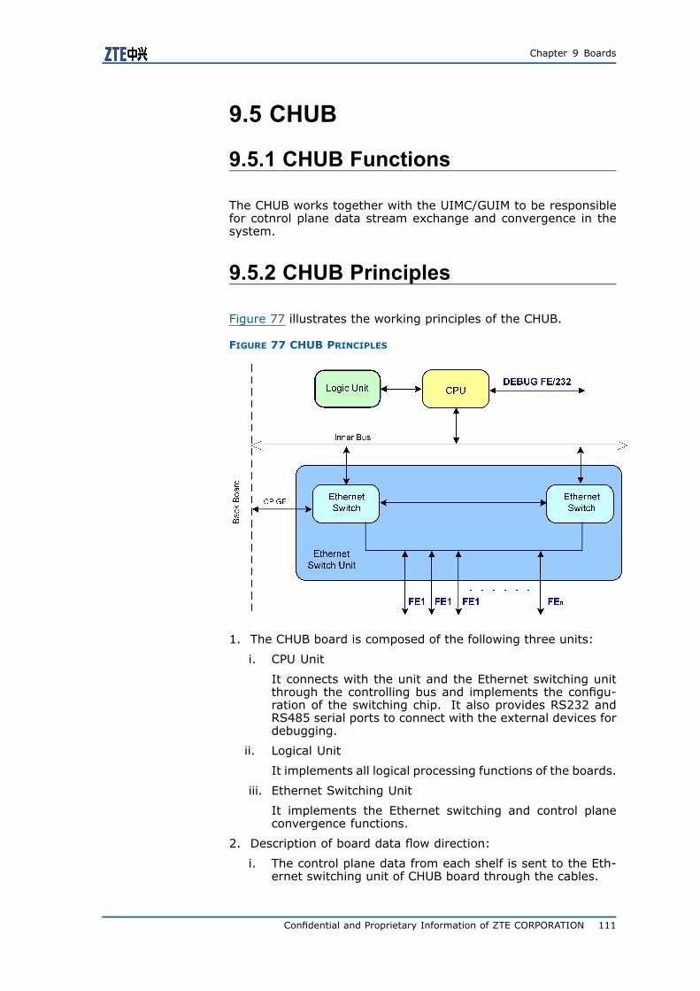
Chapter 9 Boards
9.5 CHUB
9.5.1 CHUB Functions
The CHUB works together with the UIMC/GUIM to be responsiblefor cotnrol plane data stream exchange and convergence in thesystem.
9.5.2 CHUB Principles
Figure 77 illustrates the working principles of the CHUB.
FIGURE 77 CHUB PRINCIPLES
1. The CHUB board is composed of the following three units:
i. CPU Unit
It connects with the unit and the Ethernet switching unitthrough the controlling bus and implements the configu-ration of the switching chip. It also provides RS232 andRS485 serial ports to connect with the external devices fordebugging.
ii. Logical Unit
It implements all logical processing functions of the boards.
iii. Ethernet Switching Unit
It implements the Ethernet switching and control planeconvergence functions.
2. Description of board data flow direction:
i. The control plane data from each shelf is sent to the Eth-ernet switching unit of CHUB board through the cables.
Confidential and Proprietary Information of ZTE CORPORATION 111

ZXG10 iBSC Structure and Principle
ii. The data is sent to UIMC board of the control shelf throughGE and then distributes to each CMP board for processing,and vice versa.
9.5.3 CHUB Panel
The rear boards of CHUB are RCHB1 and RCHB2, which jointlyprovide external interfaces for the CHUB.
Figure 78 illustrates the panels of CHUB-related boards.
112 Confidential and Proprietary Information of ZTE CORPORATION

Chapter 9 Boards
FIGURE 78 PANELS OF CHUB RELATED BOARDS
1. Front CHUB Panel2. RCHB1 Panel (version 040501)3. RCHB2 Panel (version 040501)
4. RCHB1 Panel (version 040502)5. RCHB2 Panel (version 040502)
9.5.4 CHUB Interfaces
The CHUB board provides 46 FE interfaces and one Gigabit inter-face.
Table 24 illustrates interfaces related to the CHUB board.
Confidential and Proprietary Information of ZTE CORPORATION 113

ZXG10 iBSC Structure and Principle
TABLE 24 CHUB RELATED INTERFACES
PositionInterfaceName
Direc-tion Description
FE1-8Bi-Direc-tional
FE9-16Bi-Direc-tional
FE17-24Bi-Direc-tional
Connects to the controlplane port of the UIM
Rear BoardRCHB1 Panel(version040501)
DEBUG-FE/232
Bi-Direc-tional
CPU debugging net-work/serial port thatconnects to the debug-ging computer
FE25-32Bi-Direc-tional
FE33-40Bi-Direc-tional
FE41-46Bi-Direc-tional
Connects to the controlplane port of the UIM
FE43, FE44, FE45 andFE46 are used for trunkpurposes, and arecurrently not used.
RCHB2 Panel(version040501)
DEBUG-FE/232
Bi-Direc-tional
CPU debugging net-work/serial port thatconnects to the debug-ging computer
Odd FE1-15Bi-Direc-tional
Odd FE17-31Bi-Direc-tional
Odd FE33-45Bi-Direc-tional
Connects to the controlplane port of the UIM
Odd FE43 and OddFE45 are used for trunkpurposes, and arecurrently not used.
RCHB1 Panel(version040502)
DEBUG-FE/232
Bi-Direc-tional
CPU debugging net-work/serial port thatconnects to the debug-ging computer
Even FE2-16Bi-Direc-tional
Even FE18-32Bi-Direc-tional
Even FE34-46Bi-Direc-tional
Connects to the controlplane port of the UIM
Even FE44 and EvenFE46 are used for trunkpurposes, and arecurrently not used.
RCHB2 Panel(version040502)
DEBUG-FE/232
Bi-Direc-tional
CPU debugging net-work/serial port thatconnects to the debug-ging computer
114 Confidential and Proprietary Information of ZTE CORPORATION

Chapter 9 Boards
Note:
RCHB1 (version 040501) and RCHB2 (version 040501) shall beused together; RCHB1 (version 040502) and RCHB2 (version040502) shall be used together;
Rear boards of version 040501 cannot be used together with rearboards of version 040502.
9.5.5 CHUM Buttons
Table 25 introduces buttons on the panel of the CHUB board.
TABLE 25 CHUB PANEL BUTTONS
Button Description
RST Reset switch
EXCH Active/standby switchover switch
9.5.6 CHUB Indicators
The CHUB board has 50 indicators on its panel, as shown in Table26.
TABLE 26 CHUB INDICATORS
Indicator Color Meaning Description
RUN GreenRunning indi-cator
See "IndicatorStatus Descrip-tion".
ALM RedAlarm indica-tor
See "IndicatorStatus Descrip-tion".
ACT Green
Ac-tive/standbystatus indica-tor
On: the boardis active.
Off: the boardis standby.
Confidential and Proprietary Information of ZTE CORPORATION 115

ZXG10 iBSC Structure and Principle
Indicator Color Meaning Description
ENUM YellowBoard extrac-tion indicator
Solid on: themicroswitchis open; theboard is notin positionor versionfiles are notdownloaded.
Flashing at5 Hz (quickflashing): themicroswitchgenerates analarm becauseit is openedwhen the boardis still running.
Flashing at1 Hz (slowflashing): theboard can beextracted. Themicroswitch isopened whenthe board isrunning, andthe board is instandby modeor release theresource.
Solid off: themicroswitch isnormal.
L1-L46 Green
46-path Con-trol PanelConcatena-tion InterfaceStatus Indi-cator
ON:correspondingcontrol planeconcatenationinterfaces areconnected.
OFF:correspondingcontrol planeconcatenationinterfaces arenot connected.
9.6 ICM
9.6.1 ICM Functions
The Integrated Clock Module (ICM) provides the following func-tions.
� Responsible for system clock supply and external synchroniza-tion. The board extracts clock reference via the A interface and
116 Confidential and Proprietary Information of ZTE CORPORATION

Chapter 9 Boards
drives multiple channels of clock reference signals for use byeach interface unit.
� Receives GPS satellite signals and extract 1PPS signals and re-lated TOD messages. The 1PPS signals are used as referencefor phase lockup in order to create PP2S,19.6608MHz and 8 Kclock references for iBSC.
� Support BITS, one path of circuit (8 K), two paths of GPS8K(from this board and the external GPS) as local clock refer-ences.
� Supports background or manual selection of clock references,including BITS, line (8 K), GPS, local (Level 2 or Level 3); sup-ports software shielding of manual switchover.
� Adopts the loose coupling phase lockup system with four workmodes: CATCH, TRACE, HOLD and FREE.
� Outputs Level 3 clock.
� Provides alarm signals for the loss alarm reference and candetermine whether clock quality is degraded.
� Supports active/standby changeover.
Compared with the CLKG board, the ICM has the GPS function,which provides GPS satellite information for the positioning func-tion of the system and also adds a clock reference to the system.
9.6.2 ICM Principles
Figure 79 illustrates the working principles of the ICM board.
FIGURE 79 ICM WORKING PRINCIPLES
1. The ICM board is composed of the following five units:
i. Main control unit
It manages the board and communicates with the systemcontrol unit. It implements the core clock control algo-rithm, and controls the output clock signals and selects thereference according to the phase lock unit.
Confidential and Proprietary Information of ZTE CORPORATION 117

ZXG10 iBSC Structure and Principle
ii. Reference selection unit
It selects the proper reference among several options underthe control of the main control unit. The clock reference canbe the 8 KHz frame synchronization signals from the DTB orSDTB, 2 MHz/2 Mbits from the Building Integrated TimingSupply (BITS) or GPS signals.
iii. Voltage control crystal oscillator unit
It is made up of thermostatic crystal oscillator that meetslevel-three clock standard. It provides high precision clocksource for the board.
iv. Phase lock unit
It makes phase comparison between regulation clock sig-nal and input reference. It also provides quantization datafor the main unit to control the voltage control crystal oscil-lator. The phase locking system adopts the loose couplingmechanism.
v. Active/standby switching unit
It implements active/standby switching of the boards,which imposes acceptable impact on the clock. The activeand standby ICMs are locked to the same reference forsmooth switching.
2. Description of board data flow direction:
i. Perform phase lock by selecting a path of input clock ref-erence. The output is 16 M and has frame head signals,which are required by the timing, and is distributed to theUIMU after balance driving.
ii. Obtain the new PP2S through pulse extension on the re-ceived PP2S and 16 CHIP signals, and then distribute toeach shelf.
iii. Extract 1PPS signals from received GPS signals, and use the1PPS signals to produce the system required PP2S, 19.6608MHz and system 8 K clock reference for reference phaselockup, and then sends these references to each shelf.
9.6.3 ICM Panel
The rear boards of ICM are RCKG1 and RCKG2. Figure 80 illus-trates the ICM board and its rear boards.
118 Confidential and Proprietary Information of ZTE CORPORATION

Chapter 9 Boards
FIGURE 80 ICM BOARDS AND REAR BOARDS
1. Front board ICM Panel2. Front board ICM Layout3. RCKG1 Panel (version 040503)
4. RCKG2 Panel (version 040502)5. RCKG1 Panel (version 071200)6. RCKG2 Panel (version 071200)
9.6.4 ICM Interfaces
Table 27 illustrates interfaces related to the ICM board.
TABLE 27 ICM RELATED INTERFACES
Position Interface Name Direction Description
GPS Input
Connects with theGPS antenna to re-ceive GPS satellitesignals
PP2S Output
The GPS modulesends PP2S signalsto the front boardpanel
5M Output
The GPS modulesends 10M signals tothe front board panel
ICM Panel MONBi-Direc-tional
GPS module to frontboard debug serialport
Confidential and Proprietary Information of ZTE CORPORATION 119

ZXG10 iBSC Structure and Principle
Position Interface Name Direction Description
CLKOUT Output
CLKOUT Output
Six clock outputinterfaces thatconnect withresource and controlshelves
One CLKOUTinterface outputsa one-to-six cable;a shelf has twoUIM/GUIM boardsthat use one groupof active/standbyclocks (includingtwo paths of 16M, two paths of 8K and two pathsof PP2S signals).Therefore, oneCLKOUT interfacecan connect withthree shelves.The RCKG1 boardhas two CLKOUTinterfaces providingsix clock outputlines, that is , itcan connect withsix shelves.
8 KIN1 Input
Two 8K referenceinput interfaces.When SDTB2 pro-vides the clock refer-ence, it connectswith the 8KOUT/DE-BUG-232 interfaceof RGIM1.WhenDTB provides theclock reference,it connects withthe 8KOUT/DE-BUG-232 inter-face of RDTB.WhenSPB2 provides theclock reference, itconnects with the8KOUT/CPU1-RS232interface of RSPB.
8 KIN2 Input
Two 8K reference in-put connecting theGPS clock refer-ence To ensure clockreference redun-dancy, the 8KIN2 in-terface can also in-put line 8 K clockreference as thebackup clock.
RCKG1Panel(version040503)
120 Confidential and Proprietary Information of ZTE CORPORATION

Chapter 9 Boards
Position Interface Name Direction Description
2 Mbps/2 MHz Input
One 2 M bits/2 MHzinput that connectswith the externalBITS clock reference
75 Ω coaxialcable or 120 Ωtwisted-pair cable,with a maximumtransmissiondistance of 250 m
CLKOUT Output
CLKOUT Output
CLKOUT Output
Nine clock outputinterfaces to connectwith resource andcontrol shelves
The RCKG2 boardhas three CLKOUTinterfaces. It canprovide nine clockoutput lines thatconnect to nineshelves.
RCKG1 and RCKG2work togetherto provide clockreferences to 15shelves, whichis the maximumclock connectionsfor iBSC.
040502RCKG2 PP2S/16CHIP Input
One GPS referenceinput connecting theexternal GPS clockreference
CLKOUT Output
CLKOUT Output
Six clock outputinterfaces to connectwith resource andcontrol shelves
One CLKOUTinterfaces outputsa one-to-six cable;one shelf has twoUIM/GUIM boardswith two clocksockets, so oneCLKOUT interfacecan connect withthree shelves,namely, threeclock output lines.The RCKG1 boardhas two CLKOUTinterfaces providingsix clock outputlines, that is , itcan connect withsix shelves.
RCKG1 and RCKG2of the same versionoutputs one group
071200RCKG1
Confidential and Proprietary Information of ZTE CORPORATION 121

ZXG10 iBSC Structure and Principle
Position Interface Name Direction Descriptionof active/standbyclocks that connectto the rear boards ofthe UIM and GUIMboards in the activeand standby slots.
8 KIN1 Input
8 K reference in-putwhen SDTB2 pro-vides the clock refer-ence, it connectswith the 8KOUT/DE-BUG-232 interfaceof RGIM1.WhenDTB provides theclock reference,it connects withthe 8KOUT/DE-BUG-232 inter-face of RDTB.WhenSPB2 provides theclock reference, itconnects with the8KOUT/CPU1-RS232interface of RSPB.
RS232Bi-Direc-tional
System debuggingserial port that con-nects to the debug-ging computer
BITS REF Input
1*2 M bits or 2MHz reference clockinput, connectingexternal BITS clockreference
75 Ω coaxialcable or 120 Ωtwisted-pair cable,with a maximumtransmissiondistance of 250 m
CLKOUT Output
CLKOUT Output
Six clock outputinterfaces to connectwith resource andcontrol shelves
One CLKOUTinterfaces outputsa one-to-six cable;one shelf has twoUIM boards with 2clock sockets, so oneCLKOUT interfacecan connect withthree shelves,namely, three clockoutput lines.TheRCKG1 boardhas two CLKOUTinterfaces providingsix clock outputlines, that is , it
RCKG2Panel(version071200)
122 Confidential and Proprietary Information of ZTE CORPORATION

Chapter 9 Boards
Position Interface Name Direction Descriptioncan connect withsix shelves.
RCKG1 and RCKG2of the same versionoutputs one groupof active/standbyclocks that connectto the rear boards ofthe UIM and GUIMboards in the activeand standby slots.
8 KIN2 Input
8K reference in-putwhen SDTB2 pro-vides the clock refer-ence, it connectswith the 8KOUT/DE-BUG-232 interfaceof RGIM1.WhenDTB provides theclock reference,it connects withthe 8KOUT/DE-BUG-232 inter-face of RDTB.WhenSPB2 provides theclock reference, itconnects with the8KOUT/CPU1-RS232interface of RSPB.
RS232Bi-Direc-tional
System debuggingserial port that con-nects to the debug-ging computer
BITS REF Input
One 2 M bits or 2MHz reference clockinput, connectingexternal BITS clockreference
75 Ω coaxialcable or 120 Ωtwisted-pair cable,with a maximumtransmissiondistance of 250 m
Note:
RCKG1 version 040503 and RCKG2 version 040503 work together,using two sets of 8 K clock references from RCKG1; RCKG1 version071200 and RCKG2 version 071200 work together, using respec-tively a set of 8 K clock reference a set of BITS clock reference.
Rear boards of version 0405xx cannot be used together with rearboards of version 071200.
Confidential and Proprietary Information of ZTE CORPORATION 123

ZXG10 iBSC Structure and Principle
9.6.5 ICM Buttons
Table 28 illustrates buttons on the panel of the ICM board.
TABLE 28 ICM BUTTONS
Name Description
RST Reset switch
EXCH Active/standby switchover switch
MANEN
To enable manual selection of clock reference
After pressing this button, the MANI indicator is ONand manual clock reference selection is enabled.
MANSL
Manual selection of clock reference
Press the MANEN button before selectingthe clock reference.
When the MANI indicator is ON, press theMANSL button to select the clock referenceone by one (panel indicators 8 K1, 8 K2, 8K3 and NULL will be turned on).
9.6.6 ICM Indicators
The ICM has 23 indicators on its panel, as shown in Table 29.
TABLE 29 ICM INDICATORS
Indicator Color Meaning Description
RUN Green Running indicatorSee "Indicator StatusDescription".
ALM Red Alarm indicatorSee "Indicator StatusDescription".
ENUM YellowBoard extractionindicator
Solid on: themicroswitch is open;the board is not inposition or version filesare not downloaded.
Flashing at 5 Hz(quick flashing): themicroswitch generatesan alarm because it isopened when the boardis still running.
Flashing at 1 Hz (slowflashing): the boardcan be extracted. Themicroswitch is openedwhen the board isrunning, and the board
124 Confidential and Proprietary Information of ZTE CORPORATION

Chapter 9 Boards
Indicator Color Meaning Descriptionis in standby mode orrelease the resource.
Solid off: themicroswitch is normal.
ACT GreenActive/standbystatus indicator
On: the board is active.
Off: the board isstandby.
Bps1 GreenClock referenceindicator
Indicates the clockreference selectedby the ICM.
If it is ON, then thefirst path is selected,which uses the 2 Mbpsclock reference signalin HDB3 code providedby the BITS device
Bps2 GreenClock referenceindicator
Indicates the clockreference selectedby the ICM.
If it is ON, then thesecond path is selected,which uses the 2 Mbpsclock reference signalin HDB3 code providedby the BITS device
Hz1 GreenClock referenceindicator
Indicates the clockreference selectedby the ICM.
If it is ON, then thefirst path is selected,which uses the 2 MHzclock reference signaltransmitted in thedifferential TTL mode.
Hz2 GreenClock referenceindicator
Indicates the clockreference selectedby the ICM.
If it is ON, then thesecond path is selected,which uses the 2 MHzclock reference signaltransmitted in thedifferential TTL mode.
8 K1 GreenClock referenceindicator
Indicates the clockreference selectedby the ICM.
If it is ON, then 8 Kclock extracted fromthe line is selected.
Confidential and Proprietary Information of ZTE CORPORATION 125

ZXG10 iBSC Structure and Principle
Indicator Color Meaning Description
8 K2 GreenClock referenceindicator
Indicates the clockreference selectedby the ICM.
If it is ON, then the8 K clock providedby the external GPSis selected.
8 K3 GreenClock referenceindicator
Indicates the clockreference selectedby the ICM.
If it is ON, then the 8K clock from the GUIMor UIMC is selected.
8 K4 GreenClock referenceindicator
Indicates the clockreference selectedby the ICM.
If it is ON, then the8 K clock provided byGPS on the local boardis selected.
NULL GreenClock referenceindicator
Indicates the clockreference selectedby the ICM.
If it is ON, then thesystem has no externalclock reference and is inthe free oscillationmode.
QUTD RedReference degra-dation indicator
If it is ON, then clockreference has degraded.
CATCH GreenCatch status indi-cator
ON: the CLKG board isin the catch status, thatis, the CLKG board hasa reference clock signalbut is not locked on thereference signal.
TRACE GreenTrace status indi-cator
ON: the CLKG board isin the trace status, thatis, the CLKG board hasa reference clock sig-nal and is locked on thereference signal.
KEEP Green Keep status signal
ON: the CLKG board haslocked on a referencesignal, but then lost it
FREE GreenFree status indica-tor
ON: The CLKG boardhas no reference signaland has not been lockedon any reference signal,and is in the free run-ning mode.
126 Confidential and Proprietary Information of ZTE CORPORATION

Chapter 9 Boards
Indicator Color Meaning Description
MANI Green
Indicator for al-lowance of man-ual reference se-lection
ON: you can manuallyselect the clockreference
OFF: you cannotmanually select theclock reference
SCS Green
System clockreference indica-tor
Solid ON: system clockis normal.
Solid OFF: out-of-lockfor 16chip lock-phaseloop.
Quick flashing: output16chip signal isabnormal.
Slow flashing: theoutput PP2S signalis abnormal.
CCS GreenCircuit clock refer-ence indicator
Solid ON: Circuit clock12.8M PLL is lockednormally
Solid OFF: Circuit clock12.8M PLL is unlocked
ANT GreenAntenna status in-dicator
Indicates antennastatuses, includingreceiver initialization,antenna feeder openand normal
Solid ON: the antennafeeder is normal.
Solid OFF: the antennafeeder and the satelliteare and initializing isin process.
Flashing at 1 Hz:the feeder circuitryis broken
Flashing at 2 Hz :the antenna is normalbut cannot receivesatellite signals
Flashing at 0.5 Hz: thefeeder is short-circuited
Flashing at 5 Hz: nomessage is receivedduring initialization
TYPGreen/Yel-
low Mode indicator
Solid off (black): GPSmono-mode receiver
Solid on (green):GPS/GONOLASSdual-mode receiver
Solid on: GPS/GON-OLASS/Beidou regularthree-mode receiver
Confidential and Proprietary Information of ZTE CORPORATION 127

ZXG10 iBSC Structure and Principle
9.6.7 DIP Switches on the ICM Board
DIP switches S1 and S5 on the ICM board can be used to selectthe matching impedance of the input BITS clock line. By default,the impedance is 75 Ω.Table 30 illustrates the DIP switches.
TABLE 30 DIP SWITCH DESCRIPTION FOR THE ICM BOARD
Switch Configuration
Mode
DIPSwitchName 1 2 3 4
DefaultMode
S1 ON ON ON ON
75 Ω S5 ON ON ON ON
S1 ON ON ON ON
100 Ω S5 OFF OFF OFF OFF
S1 OFF OFF OFF OFF
120 Ω S5 OFF OFF OFF OFF 75 Ω
9.7 SBCX
9.7.1 SBCX Functions
The SBCX provides the following functions:
� Provides the keyboard, the mouse and the VGA interface.
� Uses Sossaman dual-path dual-core CPU with a frequency of2G Hz.
� Supports multiple operating systems, including WindowsXP/2000/2003, Linux and Solaris.
� Provides four FE interfaces and two GE interfaces for externalconnections.
� Provides four universal USB interfaces.
� Supports boot from hard disk and boot from USB drive.
9.7.2 SBCX Principles
Figure 81 illustrates the working principles of the SBCX.
128 Confidential and Proprietary Information of ZTE CORPORATION

Chapter 9 Boards
FIGURE 81 SBCX WORKING PRINCIPLES
The SBCX board is composed of the following five units:
1. CPU dual-core system: core processing module of the board,which includes the CPU, the memory controller and the mainmemory.
2. Peripheral interface unit, which provides various types of inter-faces, such as PS/2, USB and VGA.
3. External interface unit, which provides four FE interfaces andtwo GE interfaces.
4. SAS controller, which provides SAS hard disk interface and im-plements SAS RAID 0/1.
5. SAS hard disk, which stores service data.
9.7.3 SBCX Panel
The rear board of SBCX is RSVB. Figure 82 illustrates the relationsbetween them.
Confidential and Proprietary Information of ZTE CORPORATION 129

ZXG10 iBSC Structure and Principle
FIGURE 82 SBCX AND RSVB RELATIONS
1. SBCX Panel 2. RSVB Panel
9.7.4 SBCX Interfaces
Table 31 illustrates the features of SBCX related interfaces.
130 Confidential and Proprietary Information of ZTE CORPORATION

Chapter 9 Boards
TABLE 31 SBCX RELATED INTERFACES
Interfacename
AlarmDirection Description
USB1 Bi-Directional USB interface
USB2 Bi-Directional USB interface
KB InputPS/2 keyboardinterface
MS InputPS/2 mouse in-terface
VGA OutputAnalog monitorinterface
SBCX frontboard panel
Two pairs ofTX-RX - Not used
OMC1 Bi-Directional
External net-work interface1, 1000M BaseT,with a maxi-mum transmis-sion distance of50 m.
OMC2 Bi-Directional
External net-work interface2, 1000M BaseT,with a maxi-mum transmis-sion distance of50 m.
OMP1 Bi-Directional
External net-work interface3, 100M BaseT,with a maxi-mum transmis-sion distance of50 m.
HEART1 Bi-Directional
External net-work interface4, 100M BaseT,with a maxi-mum transmis-sion distance of50 m.
HEART2 Bi-Directional
External net-work interface5, 100M BaseT,with a maxi-mum transmis-sion distance of50 m.
OMP2/RS232 Bi-Directional
External net-work interface6, 100M BaseT,
RSVB rearboard panel
Confidential and Proprietary Information of ZTE CORPORATION 131

ZXG10 iBSC Structure and Principle
Interfacename
AlarmDirection Description
with a maxi-mum transmis-sion distance of50 m. Not used.
USB1 Bi-Directional USB interface
USB2 Bi-Directional USB interface
9.7.5 SBCX Buttons
Table 32 illustrates buttons on the panel of the SBCX board.
TABLE 32 SBCX PANEL BUTTONS
Name Description
RST Reset switch
EXCH Active/standby switchover switch
PWB Board power switch
ENUM1 SAS hard disk 1 unplugging switch
ENUM2 SAS hard disk 2 unplugging switch
9.7.6 SBCX Indicators
Table 33 illustrates meanings of indicators on the SBCX panel.
TABLE 33 SBCX INDICATORS
Indicator Color Meaning Description
RUN GreenRunning indi-cator
See "Indicator Status De-scription". Not used.
ALM RedAlarm indica-tor
See "Indicator Status De-scription". Not used.
132 Confidential and Proprietary Information of ZTE CORPORATION

Chapter 9 Boards
Indicator Color Meaning Description
ENUM Yellow
Board ex-traction indi-cator
Solid on: the microswitchis open; the board is notin position or version filesare not downloaded.
Flashing at 5 Hz (quickflashing): the microswitchgenerates an alarm becauseit is opened when the boardis still running.
Flashing at 1 Hz (slowflashing): the board can beextracted. The microswitchis opened when the boardis running, and the boardis in standby mode orrelease the resource.
Solid off: the microswitchis normal.
Not used.
ACT Green
Ac-tive/standbystatus indi-cator
On: the board is active.
Off: the board is standby.
Not used
HD Green IDE
IDE
IDE
No board unplugging ifthe light is on
PWR GreenPower supplyindicator
SAS1 Green SAS1
SAS 1
SAS 1
ALM1 Yellow SAS1
SAS 1
SAS 1
SAS2 Green SAS2
SAS 2
SAS 2
ALM2 Yellow SAS2
SAS 2
SAS 2
ACT Green FC1 Not used
SD Yellow FC1 Not used
ACT Green FC2 Not used
SD Yellow FC2 Not used
Confidential and Proprietary Information of ZTE CORPORATION 133

ZXG10 iBSC Structure and Principle
9.8 DTB
9.8.1 DTB Functions
The Digital Trunk Board (DTB) provides the following functions:
� Provides 32 E1/T1 links.
� Supports extraction of 8K synchronization clock from the lines,which is transferred to the CLKG/ICM board through the cableas clock reference.
� Supports 120/75 Ω impedance selection for E1 cables, and sup-ports coaxial cables and twisted-pair cables.
� Supports 100 Ω twisted-pair T1 cables.
9.8.2 DTB Principles
Figure 83 illustrates the working principles of the DTB.
FIGURE 83 DTB WORKING PRINCIPLES
1. The DTB board is composed of the following five units:
i. CPU unit, which implements board management and inter-nal connection control.
ii. Interface unit, which connects with the circuit switchingunit to provide E1/T1 lines and HW interfaces, and extractsline clock signals.
iii. Circuit switching unit, which implements the switchingfunction to the circuit HW of the interface unit.
iv. Logical processing unit, which implements the logicalswitching and adaptation in the board.
v. Clock processing unit, which receives clock signals fromthe backplane, performs frequency division and sequenceadjustment, and then use the clock signals for the localboard.
134 Confidential and Proprietary Information of ZTE CORPORATION

Chapter 9 Boards
2. Description of board data flow direction:
E1/T1 data from the line side is sent to the circuit switchingunit through the processing link layer of the interface unit, andthen sent to the GUIM board, and vice versa.
9.8.3 DTB Panel
The rear board of DTB is RDTB. Figure 84 illustrates DTB and RDTBpanels and layout.
FIGURE 84 DTB AND RDTB PANELS AND LAYOUT
1. DTB Panel2. DTB layout (version 040501)
3. RDTB Panel
The DTB has two versions: 040501 and 060201.The 060201 ver-sion has different DIP switch positions, as illustrated in Figure 85.
Confidential and Proprietary Information of ZTE CORPORATION 135

ZXG10 iBSC Structure and Principle
FIGURE 85 DTB LAYOUT (VERSION 060201)
9.8.4 DTB Interfaces
Table 34 illustrates interfaces related to the DTB.
TABLE 34 DTB RELATED INTERFACES
PositionInterfaceName Direction Description
T1/E1 1-16
T1/E1 17-32 Bi-Directional
The panel provides32 E1 interfaces forexternal connectionpurposes.
75 Ω/120 Ω E1interface; 100 ΩT1 interface.
The maximumtransmission distanceis 250 m.
RDTBPanel
8KOUT/DE-BUG-232 Bi-Directional
Leads out the 8K refer-ence clock signals andRS232 serial port de-bugging signals.
9.8.5 DTB Buttons
Table 35 introduces buttons on the panel of the DTB board.
136 Confidential and Proprietary Information of ZTE CORPORATION

Chapter 9 Boards
TABLE 35 DTB PANEL BUTTON
Button Description
RST Reset switch
9.8.6 DTB Indicators
The DTB has 36 indicators, as shown in Table 36.
TABLE 36 DTB INDICATORS
Indicator Color Meaning Description
RUN GreenRunning indica-tor
See "Indicator StatusDescription".
ALM Red Alarm indicatorSee "Indicator StatusDescription".
ENUM YellowBoard extrac-tion indicator
Solid on: themicroswitch isopen; the board isnot in position orversion files are notdownloaded.
Flashing at 5 Hz(quick flashing): themicroswitch generatesan alarm because itis opened when theboard is still running.
Flashing at 1 Hz (slowflashing): the boardcan be extracted. Themicroswitch is openedwhen the board isrunning, and theboard is in standbymode or release theresource.
Solid off: themicroswitch is normal.
ACT GreenActive/standbystatus indicator
On: the board isactive.
Off: the board isstandby.
Confidential and Proprietary Information of ZTE CORPORATION 137

ZXG10 iBSC Structure and Principle
Indicator Color Meaning Description
L1~L32 GreenE1 Indicatorsfor 32 paths
OFF: this E1/T1 lineis not configured inthe database
Solid on: this E1/T1is configured in thedatabase, but it isdisconnected.
Flashing at 1 Hz: thisE1/T1 is configuredin the database, andit is connected.
9.8.7 DTB DIP Switches and Jumpers
1. Description of DTB Jumpers:
i. DTB Jumpers
The DTB (version 040501) has a path of jumper X23 fordebugging. For the position of Jumper X23 on the board,see "DTB and RDTB Panels and Layout".X23 must be dis-connected if the board is working.
The DTB (version 060201) has two paths of jumpers (X18and X19) for debugging. For their positions on the board,see "DTB Layout (Version 060201)". Short connect eitherX18 or X19 to enter the debugging mode. X18 and X19must be disconnected if the board is working.
ii. RDTB Jumpers
Figure 86 illustrates jumpers on the RDTB.
138 Confidential and Proprietary Information of ZTE CORPORATION

Chapter 9 Boards
FIGURE 86 RDTB JUMPERS
On the RDTB, the E1 cable works in the 75 Ω unbalancedcoaxial transmission mode by default. The sending endis grounded through the jumper. The receiving end isconnected to a capacitor and then grounded through thejumper. Jumpers X9–X16 are used to complete suchsettings.
Table 37 illustrates the settings of Jumpers X9 through X16.
TABLE 37 X9-X16 PIN CONNECTION
X9-X16 PinConnection Definitions
1-2Connect E1_TXN-R to the protectionground (Path N)
3-4Connect E1_RXN-R to the protectionground (Path N)
5-6Connect E1_TXN+1-R to the protec-tion ground (Path N+1)
7-8Connect E1_RXN+1-R to the protec-tion ground (Path N+1)
9-10Connect E1_TXN+2-R to the protec-tion ground (Path N+2)
11-12Connect E1_RXN+2-R to the protec-tion ground (Path N+2)
Confidential and Proprietary Information of ZTE CORPORATION 139

ZXG10 iBSC Structure and Principle
X9-X16 PinConnection Definitions
13-14Connect E1_TXN+3-R to the protec-tion ground (Path N+3)
15-16Connect E1_RXN+3-R to the protec-tion ground (Path N+3)
Note:
If the E1 line uses 120 ΩPCM line balanced transmissionmode, the short-circuit block at X9–X16 on the RDTB needsto be removed.
2. Board DIP Switch Description
Table 38 illustrates the DIP switches on the DTB.
TABLE 38 DIP SWITCHES ON THE DTB
SwitchConfiguration
DefaultLocation
DIPSwitch Purpose
M-o-d-e 1 2 3 4 1 2 3 4
75Ω
O-N
O-N
O-N
O-N
S1~S6
S9
S12
Used to set theresistances thatmatch the impe-dances of differentE1 paths to 75Ω or120 Ω.
120Ω
O-F-F
O-F-F
O-F-F
O-F-F
O-N
O-N
O-N
O-N
75Ω
O-N
O-N
O-N
O-N
S7
S8
Used for report-ing the receivingmatching impe-dance of the corre-sponding E1 chipto the CPU.
120Ω
O-F-F
O-F-F
O-F-F
O-F-F
O-N
O-N
O-N
O-N
140 Confidential and Proprietary Information of ZTE CORPORATION

Chapter 9 Boards
SwitchConfiguration
DefaultLocation
DIPSwitch Purpose
M-o-d-e 1 2 3 4 1 2 3 4
S-H-O-R-TH-A-U-L
O-N
O-N
O-N
O-N
S10
S11
Used for reportingthe long/short wirestatus of each E1chip to the CPU.
L-O-N-GH-A-U-L
O-F-F
O-F-F
O-F-F
O-F-F
O-N
O-N
O-N
O-N
1. Each path of S7, S8 DIP is associated with an E1 chip: S7 is associatedwith 1-4 E1 chips (E1 Path 1 to 16); S8 is associated with 5-8 E1 chips(E1 Path 17 to 32). Upon power-on, the CPU reads this information andinitializes different E1 chips accordingly.
2. Each path of S10 and S11 DIP is associated with four E1 chips: S10 isassociated with 1-4 E1 chips (E1 Path 1 to 16); S11 is associated with5-8 E1 chips (E1 Path 17 to 32). Upon power-on, the CPU reads thisinformation and initialized different E1 chips accordingly.
9.9 SDTB2
9.9.1 SDTB2 Functions
The SDTB2 acts as the digital trunk interface board. It providestwo 155M STM-1 standard interfaces.
Its functions are as follows:
� Provides 2 155M STM-1 standard interfaces.
� Supports CAS and CCS, and provides an access processing ca-pacity equal to 126 E1 lines or 168 T1 lines.
� Outputs two differential 8 K synchronous clock signals for thereference of the clock board
9.9.2 SDTB2 Principles
Figure 87 illustrates the working principles of the SDTB2 board.
Confidential and Proprietary Information of ZTE CORPORATION 141

ZXG10 iBSC Structure and Principle
FIGURE 87 SDTB2 WORKING PRINCIPLES
1. The SDTB2 board is composed of the following five units:
i. CPU unit, which implements board management and inter-nal connection control.
ii. Interface unit, which connects with the circuit switchingunit and provides STM-1 interfaces.
iii. Circuit switching unit, which implements the switchingfunction to the circuit HW of the interface unit.
iv. Logical processing unit, which implements the logicalswitching and adaptation in the board.
v. Clock processing unit, which receives the clock referencefrom the system clock board and provides clock referencesignals obtained from STM-1.
2. Description of board data flow direction:
Observed from the reception direction, STM-1 optical data fromthe line side is processed by the Interface unit and then sentto the Circuit Switching Unit. The data is switched and thensent to the GUIM board.
The data flow on the sending direction is vice versa.
9.9.3 SDTB2 Panel
Figure 88 illustrates the panels of the SDTB2 board and its rearboard.
142 Confidential and Proprietary Information of ZTE CORPORATION

Chapter 9 Boards
FIGURE 88 PANELS OF SDTB2 AND ITS REAR BOARD
1. SDTB2 Panel2. RGIM1 Panel
Confidential and Proprietary Information of ZTE CORPORATION 143

ZXG10 iBSC Structure and Principle
Note:
The rear board is not needed when you do not need to extract 8 Kclock reference from the SDTB2 board; Use RGIM1 when you needto extract 8 K clock reference from the SDTB2 board.
9.9.4 SDTB2 Interfaces
Table 39 illustrates interfaces on the SDTB2 board.
TABLE 39 SDTB2 RELATED INTERFACES
Position Interface
Di-rec-tion Description
TR1-TX1
Bi-Di-rec-tional
SDTB2 frontboard panel TR2-TX2
Bi-Di-rec-tional
155M STM-1 standardinterface
Single module S-1.1
Wavelength: 1310 nm
Transmitting power: -14~ -8 dBm
Receiving sensitivity:≤ -31 dBm
Maximum receivingpower: -8 dBm
Maximum transmissiondistance: 15 km
RGIM1 rearboard panel
8KOUT/DE-BUG-232
Bi-Di-rec-tional
Leads out the 8K referenceclock signals and RS232 se-rial port debugging signals
9.9.5 SDTB2 Buttons
Table 40 illustrates buttons on the panel of the SDTB2 board.
TABLE 40 SDTB2 PANEL BUTTONS
Name Description
EXCHManual exchange switch for active/standbySDTB2
RST Reset switch
144 Confidential and Proprietary Information of ZTE CORPORATION

Chapter 9 Boards
9.9.6 SDTB2 Indicators
The SDTB2 board has eight indicators, as shown in Table 41.
TABLE 41 SDTB2 INDICATORS
Indicator Color Meaning Description
RUN GreenRunning indi-cator
See "Indicator Sta-tus Description".
ALM RedAlarm indica-tor
See "Indicator Sta-tus Description".
ENUM YellowBoard extrac-tion indicator
Solid on: themicroswitch isopen; the boardis not in position orversion files are notdownloaded.
Flashing at 5 Hz(quick flashing):the microswitchgenerates an alarmbecause it is openedwhen the board isstill running.
Flashing at 1 Hz(slow flashing):the board can beextracted. Themicroswitch isopened when theboard is running,and the board isin standby mode orrelease the resource.
Solid off: themicroswitch isnormal.
ACT Green
Board ac-tive/standbyindicator
ON: the board isactive;
Off: the board isstandby.
ACT Green
Optical mod-ule 1 ac-tive/standbyindicator
ON: the opticalinterface is active;
OFF: the opticalinterface is standby;
This indicators isclose to the SDindicator
Confidential and Proprietary Information of ZTE CORPORATION 145

ZXG10 iBSC Structure and Principle
Indicator Color Meaning Description
SD GreenOptical signal1 indicator
ON: the opticalboard has receivedoptical signals
OFF: the opticalboard has notreceived opticalsignals
ACT Green
Optical mod-ule 2 ac-tive/standbyindicator
ON: the opticalinterface is active;
OFF: the opticalinterface is standby;
This indicators isclose to the SDindicator
SD GreenOptical signal2 indicator
ON: the opticalboard has receivedoptical signals
OFF: the opticalboard has notreceived opticalsignals
9.10 SPB2
9.10.1 SPB2 Functions
According to its functions, the SPB2 board can be classified into theLAPD processing board (LAPD2), the signaling processing board(SPB2) and the Gb interface processing board (GIPB2).
The LAPD2 board processes LAPD signaling. LAPD signaling datafrom the BTS are received by the DTB/SPB/SPB2 board, and thenswitched to the LAPD2 board through the circuit switching net onthe UIM board in the local resource shelf or the GUIM board in thelocal Gigabit resource shelf. The LAPD2 completes the processingof LAPD signaling data.
The SPB2 board processes MTP2 and X.25 protocols. It supportsextraction of 8 K synchronization clock from the lines, which istransferred to the CLKG board through the cable as clock refer-ence.
The GIPB2 board processes the FR, NS and partial BSSGP protocolsfor the GPRS, and provides Gb interfaces.
The SPB2 board provides 16 external E1/T1 links and supports thefollowing cables:
� Supports 120/75 Ω impedance selection for E1 cables, and sup-ports coaxial cables and twisted-pair cables.
� Supports 100 Ω twisted-pair T1 cables.
146 Confidential and Proprietary Information of ZTE CORPORATION

Chapter 9 Boards
9.10.2 SPB2 Principles
Figure 89 illustrates the working principles of the SPB2 board.
FIGURE 89 SPB2 WORKING PRINCIPLES
1. The SPB2 board is composed of the following five units:
i. Interface unit, which connects with the switching unit andprovides E1 interfaces.
ii. Circuit switching unit, which implements the switching be-tween interface unit circuits and backplane circuits.
iii. CPU unit, which implements signaling processing, boardmanagement and internal connection control.
iv. Ethernet switching unit, which implements control planeand user plane data switch and provides FE interfaces.
v. Clock unit, which extracts line clock signals.
2. Description of board data flow direction:
Data from the E1 interface or the backplane is processed bythe Interface Unit and then switched at the Circuit SwitchingUnit. Then the data is sent to the CPU Unit, and sent to otherboards via the Switch Unit.
9.10.3 SPB2 Panel
Figure 90 illustrates the panel of the SPB2 board and its rear board.
Confidential and Proprietary Information of ZTE CORPORATION 147

ZXG10 iBSC Structure and Principle
FIGURE 90 PANELS OF SPB2 AND ITS REAR BOARDS
1. SPB2 Panel 2. RSPB Panel
9.10.4 SPB2 Interfaces
Table 42 illustrates interfaces on the SPB2 board.
TABLE 42 SPB2 RELATED INTERFACES
PositionInterfaceName Direction Description
T1/E1 1-16Bi-Direc-tional
The panel provides16 E1 interfaces forexternal connectionpurposes.
75 Ω/120 Ω E1interface; 100 ΩT1 interface.
The maximumtransmission distanceis 250 m.RSPB Panel
148 Confidential and Proprietary Information of ZTE CORPORATION

Chapter 9 Boards
PositionInterfaceName Direction Description
8KOUT/C-PU1-RS232
Bi-Direc-tional
Leads out the 8K resto-ration clock signals andRS232 serial port de-bugging signals
CPU2-RS232
Bi-Direc-tional
Leads out RS232 serialport debugging signals
CPU3-RS232
Bi-Direc-tional
Leads out RS232 serialport debugging signals
CPU4-RS232
Bi-Direc-tional
Leads out RS232 serialport debugging signals
9.10.5 SPB2 Buttons
Table 43 introduces buttons on the panel of the SPB2 board.
TABLE 43 SPB2 PANEL BUTTONS
Button Description
RST Reset switch
9.10.6 SPB2 Indicators
The SPB2 board has ICM has 20 indicators, as shown in Table 44.
TABLE 44 SPB2 INDICATORS
Indicator Color Meaning Description
RUN GreenRunning in-dicator
See "Indicator Status Descrip-tion".
ALM RedAlarm indi-cator
On: An alarm exists onthe board.
Off: No alarm is generatedon the board
See "Indicator StatusDescription" for details.
Confidential and Proprietary Information of ZTE CORPORATION 149

ZXG10 iBSC Structure and Principle
Indicator Color Meaning Description
ENUMYel-low
Board ex-traction in-dicator
Solid on: the microswitchis open; the board is not inposition or version files arenot downloaded.
Flashing at 5 Hz (quick flashing):the microswitch generates analarm because it is opened whenthe board is still running.
Flashing at 1 Hz (slow flashing):the board can be extracted. Themicroswitch is opened whenthe board is running, and theboard is in standby mode orrelease the resource.
Solid off: the microswitchis normal.
ACT Green
Active/sta-ndby statusindicator
On: the board is active.
Off: the board is standby.
L1~L16 Green
E1 Indica-tors for 16lines
OFF: this E1/T1 line is notconfigured in the database
Solid on: this E1/T1 isconfigured in the database,but it is disconnected.
Flashing at 1 Hz: this E1/T1is configured in the database,and it is connected.
Flashing at 5 Hz: this E1/T1already has link services.
9.11 GIPI
9.11.1 GIPI Functions
The IP interfaces between iBSC and the BTS, the SGSN and theMSC/MGW are provided by the single-port GE interface boardGIPI.Each GIPI provides one GE interface or four FE interfaces forexternal connection purposes.
The GIPI board can be classified into four functional boards accord-ing to functions provides: Abis Gigabit IP Interface Board (IPBB),A-interface Gigabit IP Interface Board for signaling(IPAB), A-inter-face Gigabit IP Interface Board for signaling and service, and GbGigabit IP Interface Board (IPGB).
9.11.2 GIPI Principles
Figure 91 illustrates the working principles of the GIPI.
150 Confidential and Proprietary Information of ZTE CORPORATION

Chapter 9 Boards
FIGURE 91 GIPI WORKING PRINCIPLES
1. The GIPI board is composed of three units:
i. Processing unit
It processes related protocols and separates the user planefrom the control plane.
ii. Logical Unit
It implements all logical processing functions of the boards.
iii. Interface Unit
It provides one external GE interface and one debuggingEthernet interface.
2. Description of board data flow direction:
The Interface Unit receives data and sends it to the serviceprocessing unit, which separates user plane data from controlplane data. User plane data is then sent to the GUP2 throughthe user plane switch network, and control plane data is sentto the CMP through the control plane switch network.
9.11.3 GIPI Panel
The rear board of the TIPI board is RGER.Figure 92 illustrates thepanels of the GIPI board and its rear boards.
Confidential and Proprietary Information of ZTE CORPORATION 151

ZXG10 iBSC Structure and Principle
FIGURE 92 GIPI AND REAR BOARD PANELS
1. GIPI Panel2. RGER Panel
3. RMNIC Panel
Note:
The rear board of the GIPI board is usually RGER. The RMNIC boardis used only when the GIPI board is connected with the OMCB orthe MR, as required by the iBSC.
9.11.4 GIPI Interfaces
The rear board of the GIPI board, namely the RGER board, pro-vides one GE interface that connects to the external network.
Table 45 illustrates interfaces on the panel of the GIPI board.
152 Confidential and Proprietary Information of ZTE CORPORATION

Chapter 9 Boards
TABLE 45 GIPI RELATED INTERFACES
PositionInterfaceName
Direc-tion Description
GIPIPanel TX-RX
Bi-Di-rectional
GE optical interface thatconnects to the BTS, the SGSNand the MSC/MGW
It cannot simultaneously validwith the GE1 interface.
Single-mode optical port,wavelength 1310 nm,transmitting power -9.5 dBm to-3 dBm, receiving sensitivity <-20 dBm, transmission distance10 km, using LC connector.
GE1Bi-Di-rectional
GE electrical interface thatconnects to the BTS, the SGSNand the MSC/MGW
It cannot simultaneously validwith the TX-RX interface.
1000baseT electrical interfacewith a maximum transmissiondistance of 50 m.
GE2Bi-Di-rectional GE interface. Not used.
DEBUG1-232Bi-Di-rectional
Debugging Ethernet interfacethat connects with the debug-ging computer. Not used.
RGERPanel DEBUG2-232
Bi-Di-rectional
Debugging Ethernet interfacethat connects with the debug-ging computer. Not used.
The RMNIC board is used only when the GIPI board is connectedwith the OMCB or the MR, as required by the iBSC. For RMNICinterfaces, see "BIPI Related Interfaces".
9.11.5 GIPI Buttons
Table 46 shows buttons on the panel of the GLI board.
TABLE 46 GIPI PANEL BUTTONS
Button Description
RST Reset switch
EXCH Active/standby switchover switch
Confidential and Proprietary Information of ZTE CORPORATION 153
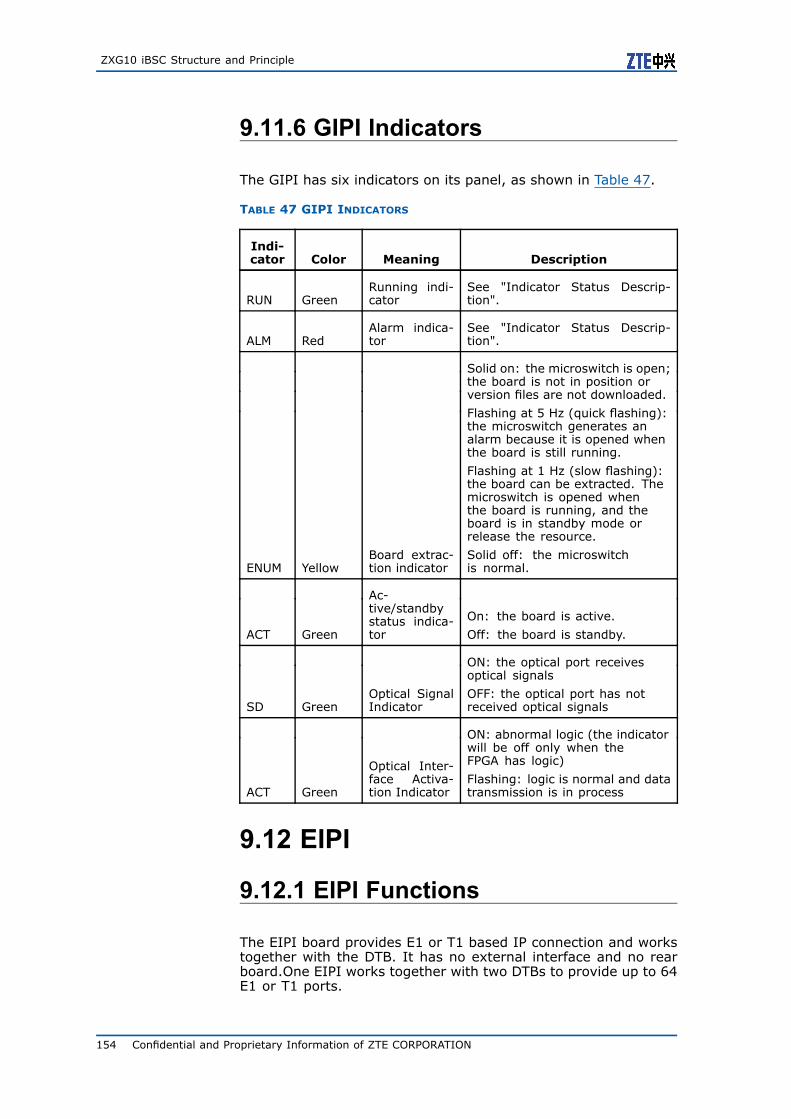
ZXG10 iBSC Structure and Principle
9.11.6 GIPI Indicators
The GIPI has six indicators on its panel, as shown in Table 47.
TABLE 47 GIPI INDICATORS
Indi-cator Color Meaning Description
RUN GreenRunning indi-cator
See "Indicator Status Descrip-tion".
ALM RedAlarm indica-tor
See "Indicator Status Descrip-tion".
ENUM YellowBoard extrac-tion indicator
Solid on: the microswitch is open;the board is not in position orversion files are not downloaded.
Flashing at 5 Hz (quick flashing):the microswitch generates analarm because it is opened whenthe board is still running.
Flashing at 1 Hz (slow flashing):the board can be extracted. Themicroswitch is opened whenthe board is running, and theboard is in standby mode orrelease the resource.
Solid off: the microswitchis normal.
ACT Green
Ac-tive/standbystatus indica-tor
On: the board is active.
Off: the board is standby.
SD GreenOptical SignalIndicator
ON: the optical port receivesoptical signals
OFF: the optical port has notreceived optical signals
ACT Green
Optical Inter-face Activa-tion Indicator
ON: abnormal logic (the indicatorwill be off only when theFPGA has logic)
Flashing: logic is normal and datatransmission is in process
9.12 EIPI
9.12.1 EIPI Functions
The EIPI board provides E1 or T1 based IP connection and workstogether with the DTB. It has no external interface and no rearboard.One EIPI works together with two DTBs to provide up to 64E1 or T1 ports.
154 Confidential and Proprietary Information of ZTE CORPORATION
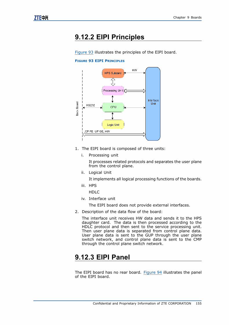
Chapter 9 Boards
9.12.2 EIPI Principles
Figure 93 illustrates the principles of the EIPI board.
FIGURE 93 EIPI PRINCIPLES
1. The EIPI board is composed of three units:
i. Processing unit
It processes related protocols and separates the user planefrom the control plane.
ii. Logical Unit
It implements all logical processing functions of the boards.
iii. HPS
HDLC
iv. Interface unit
The EIPI board does not provide external interfaces.
2. Description of the data flow of the board:
The interface unit receives HW data and sends it to the HPSdaughter card. The data is then processed according to theHDLC protocol and then sent to the service processing unit.Then user plane data is separated from control plane data.User plane data is sent to the GUP through the user planeswitch network, and control plane data is sent to the CMPthrough the control plane switch network.
9.12.3 EIPI Panel
The EIPI board has no rear board. Figure 94 illustrates the panelof the EIPI board.
Confidential and Proprietary Information of ZTE CORPORATION 155
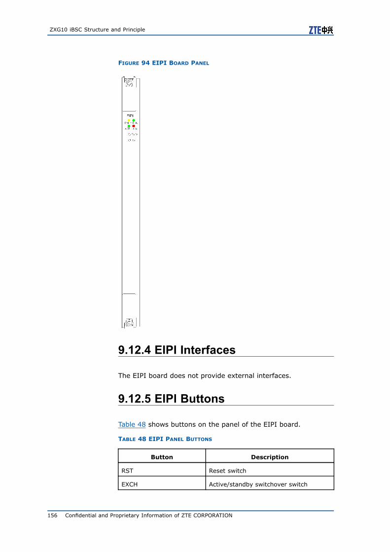
ZXG10 iBSC Structure and Principle
FIGURE 94 EIPI BOARD PANEL
9.12.4 EIPI Interfaces
The EIPI board does not provide external interfaces.
9.12.5 EIPI Buttons
Table 48 shows buttons on the panel of the EIPI board.
TABLE 48 EIPI PANEL BUTTONS
Button Description
RST Reset switch
EXCH Active/standby switchover switch
156 Confidential and Proprietary Information of ZTE CORPORATION

Chapter 9 Boards
9.12.6 EIPI Indicators
The EIPI has four indicators on its panel, as shown in Table 49.
TABLE 49 EIPI INDICATORS
Indica-tor Color Meaning Description
RUN GreenRunningindicator See "Indicator Status Description".
ALM RedAlarm in-dicator See "Indicator Status Description".
ENUM Yellow
Board ex-tractionindicator
Solid on: the microswitch is open;the board is not in position orversion files are not downloaded.
Flashing at 5 Hz (quick flashing):the microswitch generates an alarmbecause it is opened when theboard is still running.
Flashing at 1 Hz (slow flashing):the board can be extracted. Themicroswitch is opened whenthe board is running, and theboard is in standby mode orrelease the resource.
Solid off: the microswitch is normal.
ACT Green
Active/st-andby st-atus indi-cator
On: the board is active.
Off: the board is standby.
9.13 GUIM
9.13.1 GUIM Functions
The Gigabit Universal Interface Module (GUIM) performs EthernetLevel 2 switching between the control plane and the user plane inthe Gigabit resource shelf, the CS field timeslot multiplexing slotswitching and Gigabit resource shelf management. It also providesexternal interfaces for the Gigabit resource shelf.
It provides the clock drive in the resource shelf. It inputs PP2S, 8K and 16 M signals, which are sent to different slots in the Gigabitresource shelf after phase lockup to provide 16 M, 8 K and PP2Sclocks for boards in the Gigabit resource shelf.
The UGIM board performs Gigabit resource shelf management andprovides RS485 management interfaces in the Gigabit resourceshelf; It also provides board resetting and in-slot signal collectionfunctions.
Confidential and Proprietary Information of ZTE CORPORATION 157

ZXG10 iBSC Structure and Principle
9.13.2 GUIM Principles
Figure 95 illustrates the working principles of the GUIM.
FIGURE 95 GUIM WORKING PRINCIPLES
1. The GUIM board is composed of the following four units:
i. CPU Unit
It connects the time-slot switching unit, the logical unit andethernet switching unit via the control bus to implementswitching unit configuration, logical unit configuration andmanagement and GE resource shelf management.
It also provides Ethernet interfaces, RS232 and RS385 se-rial ports externally for debugging and active/standby pur-poses.
ii. Logical Unit
It implements all logical processing functions of the boards.
iii. Circuit Switching Unit (CSU)
It has the capability of 16 K circuit switching, and providesan internal circuit switching network for the GE resourceshelf.
iv. Ethernet Switching Unit
It implements the ethernet switching function of the userplane and the control plane in a GE resource shelf.
2. Description of board data flow direction:
External data, coming from each board of the shelf that con-tains the GUIM, goes into the Ethernet switching unit or thetime-slot switching unit for switching processing, and is thensent to the destination board or the level-1 switching interfaceboard.
158 Confidential and Proprietary Information of ZTE CORPORATION

Chapter 9 Boards
9.13.3 GUIM Panel
The rear boards of GUIM are RGUM1 and RGUM2. Figure 96 illus-trates the panels of the GUIM board and its rear boards.
FIGURE 96 PANELS OF GUIM BOARDS AND ITS REAR BOARDS
1. GUIM Panel2. RGUM1 Panel
3. RGUM2 Panel
9.13.4 GUIM Interfaces
Table 50 illustrates interfaces related to the GUIM board.
Confidential and Proprietary Information of ZTE CORPORATION 159

ZXG10 iBSC Structure and Principle
TABLE 50 GUIM RELATED INTERFACES
PositionInterfaceName Direction Description
GUIM PanelFour pairs ofRX-TXs
Bi-Direc-tional
The front panel opti-cal cable connects tothe GLI board of theswitching unit, userside expansion adoptsfour 1 G optical ports
FE1Bi-Direc-tional
Provides a cascade net-work interface via tworear boards in the ac-tive and standby slotsto connect to the CHUBor the UIMC in the con-trol shelf.
FE3Bi-Direc-tional
The active and standbyslots each provides oneexternal network in-terface through tworear boards in the ac-tive and standby slots.These interfaces can beused as the debuggingnetwork interfaces.
FE5Bi-Direc-tional
The active and standbyslots each providesone independent ex-ternal network inter-face through two rearboards in the activeand standby slots.
CLKIN Input
Connects to the CLKGboard and transports 8K/16 M/PP2S clock sig-nals
RGUM1 Panel DEBUG-232Bi-Direc-tional
CPU debugging serialport that connects withthe debugging machine
FE2Bi-Direc-tional
Provides one cascad-ing network interfacevia two rear boards inthe active and standbyslots. The interfaceconnects with theCHUB or UIMC in thecontrol, and can beused as the debuggingnetwork interface.
FE4Bi-Direc-tional
The active and standbyslots each providesone independent ex-ternal network inter-face through two rearRGUM2 Panel
160 Confidential and Proprietary Information of ZTE CORPORATION

Chapter 9 Boards
PositionInterfaceName Direction Description
boards in the activeand standby slots.
FE6Bi-Direc-tional
The active and standbyslots each providesone independent ex-ternal network inter-face through two rearboards in the activeand standby slots.
CLKIN Input
Connects to the CLKGboard and transports 8K/16 M/PP2S clock sig-nals
DEBUG-232Bi-Direc-tional
CPU debugging serialport that connects withthe debugging machine
Note:
FE3, FE4, FE5 and FE6 interfaces on the rear board of GUIM cannotbe used for control plane cascading connection.
9.13.5 GUIM Buttons
Table 51 introduces buttons on the panel of the GUIM board.
TABLE 51 GUIM PANEL BUTTONS
Button Description
RST Reset switch
EXCH Active/standby switchover switch
9.13.6 GUIM Indicators
Table 52 illustrates indicators on the GUIM board.
TABLE 52 GUIM INDICATORS
Indicator Color Meaning Description
RUN GreenRunning indi-cator
See "Indicator Status Descrip-tion".
ALM RedAlarm indica-tor
See "Indicator Status Descrip-tion".
Confidential and Proprietary Information of ZTE CORPORATION 161

ZXG10 iBSC Structure and Principle
Indicator Color Meaning Description
ACT Green
Ac-tive/standbystatus indica-tor
On: the board is active.
Off: the board is standby.
ENUM YellowBoard extrac-tion indicator
Solid on: the microswitchis open; the board is not inposition or version files arenot downloaded.
Flashing at 5 Hz (quickflashing): the microswitchgenerates an alarm becauseit is opened when the boardis still running.
Flashing at 1 Hz (slowflashing): the board can beextracted. The microswitchis opened when the boardis running, and the board isin standby mode or releasethe resource.
Solid off: the microswitchis normal.
ACT-P GreenPS field indi-cator
ON: the GUIM is activein the PS field
OFF: the GUIM is standbyin the PS field
ACT Green
GE interface 1status indica-tor
ON: the current opticalinterface is activated.
OFF: the current opticalinterface is not activated.
SD Green
GE interface 1optical signalindicator
ON: the optical modulereceives optical signals
OFF: the optical module hasnot received optical signals
ACT Green
GE interface 2status indica-tor
ON: the current opticalinterface is activated.
OFF: the current opticalinterface is not activated.
SD Green
GE interface 2optical signalindicator
ON: the optical modulereceives optical signals
OFF: the optical module hasnot received optical signals
ACT Green
GE interface 3status indica-tor
ON: the current opticalinterface is activated.
OFF: the current opticalinterface is not activated.
SD Green
GE interface 3optical signalindicator
ON: the optical modulereceives optical signals
OFF: the optical module hasnot received optical signals
162 Confidential and Proprietary Information of ZTE CORPORATION

Chapter 9 Boards
Indicator Color Meaning Description
ACT Green
GE interface 4status indica-tor
ON: the current opticalinterface is activated.
OFF: the current opticalinterface is not activated.
SD Green
GE interface 4optical signalindicator
ON: the optical modulereceives optical signals
OFF: the optical module hasnot received optical signals
ACT-T GreenCS field indi-cator
ON: the GUIM is activein the CS field
ON: the GUIM is standbyin the CS field
L1~ L6 Green
1~6 status in-dicator of con-trol plane cas-cade interface
ON: control plane cascadeinterfaces FE 1–6 areconnected.
OFF: control plane cascadeinterfaces FE 1–6 are notconnected.
9.14 GUP2
9.14.1 GUP2 Functions
The GUP2 board can be categorized into five types based on itsfunctions: Ater interface processing board (TIPB2), Abis interfaceprocessing board (BIPB2), A-interface processing board (AIPB),user plane processing board (UPPB2) and dual rate transcoderboard (DRTB2).
The TIPB2 board implements TDM/IP conversion at the Ater inter-face. It finds 20ms TRAU frames and form them into IP packets.
Over the STM-1 or E1 Abis interface, CS and PS services from theBTS are switched to the BIPB2 board through the UIM board in thelocal resource shelf or the GUIM board in the local Gigabit resourceshelf. The BIPB2 board searches 20ms TRU frames or PCU framesand form them into IP packets, which are sent to the TCU or theUPU for processing.Over the IP Abis interface, the BIPB2 board isalso used to process RTP.
The AIPB board processes RTP and forms data into IP packets overthe A interface.
The UPPB processes user plane protocols such as BSSGP, PDCPand GTP_U under the A/Gb mode.
The DRTB2 implements code conversion, finishes TRAU frame con-version and rate adaptation, and provides FR/EFR/HR/AMR/TFOfunction.
Confidential and Proprietary Information of ZTE CORPORATION 163

ZXG10 iBSC Structure and Principle
9.14.2 GUP2 Principles
Figure 97 illustrates the working principles of the GUP2.
FIGURE 97 GUP2 WORKING PRINCIPLES
1. The GUP2 board is composed of six units:
i. CPU Unit
It manages the board and processes signaling from Abisinterface. It also provides the control plane FE interface toconnect with external devices.
ii. Logical Unit
It implements all logical processing functions of the boards.
iii. DSP Unit
Containing multiple DSP chips, it implements transcoding,rate adaptation or data packet conversions.
iv. Ethernet Switching Unit
It implements the Ethernet connections for multiple-chipDSP and provides the user plane FE interface for externaldevices.
v. Clock Unit
It provides necessary clock signals for the units on theboard.
vi. Circuit Switching Unit
It connects the serial ports of multiple-chip DSP with thecircuit switching network.
164 Confidential and Proprietary Information of ZTE CORPORATION

Chapter 9 Boards
2. Description of board data flow direction:
Uplink and downlink data streams are opposite in directions.Take uplink streams as an example:
i. For BIPB2, the board receives TDM data from Abis interface.Then the circuit switching unit distributes received data tothe DSP unit, which converts it into IP packets that are sentto other function boards through the Ethernet.
ii. For DRTB2, the interface unit receives audio IP packetsfrom the user plane Ethernet. The packets are distributedto DSP for transcoding and rate adaptation and then trans-formed to PCM code streams that are switched to the trunkboard through the GIMU.
iii. For TIPB2, the user plane data from UIM board is dis-tributed to DSP unit through the Ethernet switching unit,which converts it into TDM data that is sent to other func-tion boards for processing.
iv. For AIPB, the user plane data from the GUIM board is dis-tributed to the DSP unit through the Ethernet switchingunit, which processes the RTP protocol and then sends itto other function boards for processing.
v. For UPPB2, user plane data from the GUIM are receivedby the board through the user plane FE/GE interface. Thedata is then distributed to the DSP unit through the Eth-ernet switching unit. The DSP unit processes related userplane protocols and then switch the data to the SPB2 boardthrough the user plane GE interface.
9.14.3 GUP2 Panel
The GUP2 board has no rear board. Figure 98 introduces the panelof the GUP2 board.
Confidential and Proprietary Information of ZTE CORPORATION 165

ZXG10 iBSC Structure and Principle
FIGURE 98 GUP2 PANEL
9.14.4 GUP2 Interfaces
The GUP2 board does not provide external interfaces.
9.14.5 GUP2 Buttons
Table 53 introduces buttons on the panel of the GUP2 board.
166 Confidential and Proprietary Information of ZTE CORPORATION

Chapter 9 Boards
TABLE 53 GUP2 PANEL BUTTON
Button Description
RST Reset switch
9.14.6 GUP2 Indicators
The GUP2 board has four indicators on its panel, as shown in Table54.
TABLE 54 GUP2 INDICATORS
Indica-tor Color Meaning Description
RUN GreenRunning in-dicator See "Indicator Status Description".
ALM RedAlarm indi-cator See "Indicator Status Description".
ENUM Yellow
Board ex-traction in-dicator
Solid on: the microswitch is open;the board is not in position orversion files are not downloaded.
Flashing at 5 Hz (quick flashing):the microswitch generates analarm because it is opened whenthe board is still running.
Flashing at 1 Hz (slow flashing):the board can be extracted. Themicroswitch is opened whenthe board is running, and theboard is in standby mode orrelease the resource.
Solid off: the microswitch is normal.
ACT Green
Active/sta-ndby statusindicator
On: the board is active.
Off: the board is standby.
9.15 GLI
9.15.1 GLI Functions
The GB Line Interface (GLI) board is located at level 1 switchingsubsystem of iBSC. It finishes physical layer adaptation, IP pack-age query, segmentation, forwarding, and flow management func-tions, and implements the interface to different resource frame andexternal interface functions.
Confidential and Proprietary Information of ZTE CORPORATION 167

ZXG10 iBSC Structure and Principle
9.15.2 GLI Principles
Figure 99 illustrates the working principles of the GLI.
FIGURE 99 GLI WORKING PRINCIPLES
1. The GLI board is composed of 5 units:
Optical Interface Unit
It provides GE optical interface and supports physical backup.
2. Logical Unit
It implements all logical processing functions of the boards.
3. Ethernet Interface Unit
It provides GE PHY and MAC functions.
4. Processing Unit
IP
5. Queue Management Unit
It implements bi-directional queue management.
6. Description of board data flow direction:
i. The GLI board receives the user plane data from the re-source shelf through the optical port.
ii. Data from the GE optical port to the board is processed bythe service processing unit and then sent to the interfaceon the switching side. The data is then sent to the PSNswitching network card.
Data from the PSN board to the GLI board is processed bythe service processing unit and then framed, after whichthe data is sent out via the corresponding optical port.
9.15.3 GLI Panel
Figure 100 shows the panel of the GLI board.
168 Confidential and Proprietary Information of ZTE CORPORATION

Chapter 9 Boards
FIGURE 100 GLI BOARD PANEL
9.15.4 GLI Interfaces
Table 55 illustrates interfaces related to the GLI board.
Confidential and Proprietary Information of ZTE CORPORATION 169

ZXG10 iBSC Structure and Principle
TABLE 55 GLI RELATED INTERFACES
PositionInterfaceName
Di-rec-tion Description
GLI frontboardpanel
8 pairs ofTX-RX
Bi-Di-rec-tional
Eight STM-1 optical ports on the frontboard panel connect to the GUIMboards in Gigabit resource shelf inorder to connect resource shelf serv-ices to the switch platform (providespairs of active/standby GE opticalports, that is, SD1 and SD2 form apair, SD3 and SD4 form a pair, andso on).
9.15.5 GLI Buttons
Table 56 introduces buttons on the panel of the GLI board.
TABLE 56 GLI PANEL BUTTONS
Button Description
RST Reset switch
EXCH Active/standby switchover switch
9.15.6 GLI Indicators
The GLI board has 20 panel indicators, as shown in Table 57.
TABLE 57 GLI INDICATORS
Indica-tor Color Meaning Description
RUN GreenRunning in-dicator See "Indicator Status Description".
ALM RedAlarm indi-cator See "Indicator Status Description".
170 Confidential and Proprietary Information of ZTE CORPORATION

Chapter 9 Boards
Indica-tor Color Meaning Description
ENUM Yellow
Board ex-traction in-dicator
Solid on: the microswitch is open;the board is not in position orversion files are not downloaded.
Flashing at 5 Hz (quick flashing):the microswitch generates analarm because it is opened whenthe board is still running.
Flashing at 1 Hz (slow flashing):the board can be extracted. Themicroswitch is opened whenthe board is running, and theboard is in standby mode orrelease the resource.
Solid off: the microswitchis normal.
ACT Green
Active/sta-ndby sta-tus indica-tor
On: the board is active.
Off: the board is standby.
ACT1-8 Green
Optical In-terface Ac-tivation In-dicator
ON: abnormal logic (the indicatorwill be off only when theFPGA has logic)
Flashing: logic is normal and datatransmission is in process
SD1-8 Green
OpticalSignal In-dicator
ON: the optical port receivesoptical signals
OFF: the optical port has notreceived optical signals
9.16 PSN
9.16.1 PSN Functions
The PSN provides the following functions:
� Provides bi-directional user plane data switch with a capacityof 40 Gbps on each direction
� Supports 1+1 load sharing.
9.16.2 PSN Principles
Figure 101 illustrates the working principles of the PSN.
Confidential and Proprietary Information of ZTE CORPORATION 171

ZXG10 iBSC Structure and Principle
FIGURE 101 PSN WORKING PRINCIPLES
1. The PSN board is composed of the following three units:
i. CPU Unit
It connects with the UIMC of the switching shelf throughthe FE interface to implement operation and maintenance.It also connects with the matrix switching unit through theinternal control bus to implement basic configuration andmanagement.
ii. Logical Unit
It implements the logical adaptation within the board.
iii. Matrix Switching Unit
It provides high-speed serial links to external devices. Italso connects with the GLI board to establish a data switch-ing channel.
2. Description of board data flow direction:
The data from each GLI board is sent to the Matrix SwitchingUnit through the high-speed serial links on the backplane. Itis switched and then sent to the destination GLI board.
9.16.3 PSN Panel
Figure 102 shows the panel of the PSN board.
172 Confidential and Proprietary Information of ZTE CORPORATION

Chapter 9 Boards
FIGURE 102 PSN BOARD PANEL
9.16.4 PSN Interfaces
The PSN board does not provide external interfaces.
9.16.5 PSN Buttons
Table 58 shows buttons on the panel of the PSN board.
Confidential and Proprietary Information of ZTE CORPORATION 173
ZXG10 iBSC Structure and Principle
TABLE 58 PSN PANEL BUTTONS
Button Description
RST Reset switch
EXCH Active/standby switchover switch
9.16.6 PSN Indicators
The PSN has four indicators on its panel, as illustrated in Table 59.
TABLE 59 PAN INDICATORS
Indica-tor Color Meaning Description
RUN GreenRunningindicator
See "Indicator Status Descrip-tion".
ALM Red Alarm indicatorSee "Indicator Status Descrip-tion".
ENUMYel-low
Board extractionindicator
Solid on: the microswitchis open; the board is not inposition or version files arenot downloaded.
Flashing at 5 Hz (quickflashing): the microswitchgenerates an alarm becauseit is opened when the boardis still running.
Flashing at 1 Hz (slow flashing):the board can be extracted.The microswitch is openedwhen the board is running, andthe board is in standby modeor release the resource.
Solid off: the microswitchis normal.
ACT GreenActive/standbystatus indicator
On: the board is active.
Off: the board is standby.
9.17 PWRD
9.17.1 PWRD Functions
The PWRD board provides the following functions:
� Provides -48 V power supply for fan and each of the shelves inthe rack.
174 Confidential and Proprietary Information of ZTE CORPORATION

Chapter 9 Boards
� Inspects the rack power supply and the environment and re-ports alarms, and monitors and controls the fans.
� Accepts monitoring and management by the OMP through theRS485 bus, and reports the monitoring information to ROMBvia the RS485 interface and give indications through panel in-dicators of the power distribution box.
9.17.2 PWRD Principles
Figure 103 illustrates the working principles of the PWRD board.
FIGURE 103 PWRD STRUCTURE
PWRD is structurally divided into the following units: a power dis-tribution unit, a main monitoring unit (PWRD), a conversion board(PWRDB) and four fan group control units.
1. The power distribution unit filters and isolates the two paths of-48 V power supplies and protects them from lightning. Thepower is then transmitted to the bus bar that supplies powerto the shelves. Before the two paths of power are integrated,samples are taken and sent to the main monitoring unit forover-voltage and under-voltage testing.
2. The main monitoring unit PWRD conducts the checks con-cerning the over-voltage/under-voltage of two paths of -48V power, rotation speed of 24 fans, environment humidity,smoke alarm, infrared alarm, access control of the cabinetand equipment room.
The power distribution unit and the main monitoring unit PWRDtogether form the power distribution subrack.
3. The fan subrack contains 2x3 fan groups and fan group controlunit.
Confidential and Proprietary Information of ZTE CORPORATION 175

ZXG10 iBSC Structure and Principle
The fan subrack obtains the -48 V power from the bus bar andsend the fan monitoring signals to the main monitoring unitPWRD.
4. The PWRDB board provides the PWRD board with the interfaceto receive the environment monitoring signals.
9.17.3 PWRD Panel
Figure 104 shows the panel of the PWRD board.
FIGURE 104 PWRD BOARD PANEL
9.17.4 DIP Switches and Jumpers onthe PWRD Board
Note:
You need to reset the board with the reset switch after changingthe DIP and jumper settings.
DIP Switch Table 60 illustrates DIP switches on the PWRD board.
TABLE 60 DIP SWITCHES ON THE PWRD BOARD
SwitchConfiguration
DefaultLocation
DIPSwitch Purpose
M-o-d-e
1(h-i-g-h) 2 3
4(l-o-w-) 1 2 3 4
S2
CONFIG Switch(set the mode to"normal" or "de-bug"; the de-fault setting is"normal")
It is used to set thework node. You donot need to change
its settings.O-N
O-FF
O-N
O-N
176 Confidential and Proprietary Information of ZTE CORPORATION

Chapter 9 Boards
SwitchConfiguration
DefaultLocation
DIPSwitch Purpose
M-o-d-e
1(h-i-g-h) 2 3
4(l-o-w-) 1 2 3 4
0O-N0
O-N
O-N
O-N
O-N
S3
SWITCH (setcommunicationaddress for 485and OMP; use4-digit switchto set the ad-dresses of 0-15,which corre-spond to theNo. of racksthat containsthe boards)
1O-FF1
O-FF
O-FF
O-FF
O-FF
O-N
O-N
O-N
O-N
Jumpers The PWRD board provides a 2×5 pin as the 485 signal jumper X8.When multiple racks are deployed in iBSC, the the 485 bus of thePWRD board should be configured according to rack location.
1. When the PWRD board is connected to the end of the 485 bus,a resistance ending is needed: Short connect the 1-2 pins andthe 9-10 pins. This is the default setting, as shown in Figure105.
FIGURE 105 JUMPER SETTINGS
2. When the PWRD board is at the middle of the 485 bus, the 485signal must be sent to the output port by short connecting the3-4 pins and the 7-8 pins.
9.18 Indicator Status DescriptionThe statuses of boards in the iBSC system are represented by dif-ferent combinations of RUN and ALM LED indicators. For specificmeanings about indicator combinations, see Table 61.
Confidential and Proprietary Information of ZTE CORPORATION 177

ZXG10 iBSC Structure and Principle
TABLE 61 MEANINGS FOR RUN AND ALM INDICATOR COMBINATIONS
StatusName RUN ALM Meaning
Running nor-mally
Flash at therate of 1 Hz Always off
Board is running nor-mally
Flash at therate of 5 Hz Always off
Version files down-loading is in process.
Flash at therate of 1 Hz
Flash at therate of 5 Hz
Version downloadfails: the board ver-sion is inconsistentwith the configuration.
Version filesdownloading Always on Always off
RELEASE version in-dicates that the ver-sion download suc-ceeds and the versionis being started.
Always offFlash at therate of 5 Hz
The self-test of theboard has failed.
Self-testfailed Always off
Flash at therate of 2 Hz
The startup of theoperation supportingsystem is failed.
Flash at therate of 5 Hz
Flash at therate of 5 Hz
The board fails to ac-quire logical address.
Flash at therate of 5 Hz
Flash at therate of 2 Hz
Basic processpower-on fails or timesout
Flash at therate of 5 Hz
Flash at therate of 1 Hz
The core data area isbeing initialized.
Flash at therate of 5 Hz
Flash at therate of 0.5 Hz
The version is incon-sistent with the hard-ware or configuration
Flash at therate of 2 Hz
Flash at therate of 5 Hz
Communications onthe media plane fails
Flash at therate of 2 Hz
Flash at therate of 2 Hz
The HW is discon-nected.
Flash at therate of 1 Hz
Flash at therate of 2 Hz
The board is discon-nected from OMP
Flash at therate of 1 Hz
Flash at therate of 1 Hz
Active/standby switch-over is in process
Alarms dur-ing running
Flash at therate of 1 Hz Always on
The hardware clock islost.
178 Confidential and Proprietary Information of ZTE CORPORATION

Figures
Figure 1 Position of iBSC in the Network ................................ 2
Figure 2 iBSC Overall Appearance ......................................... 3
Figure 3 Cabinet Layout......................................................19
Figure 4 Shelf Positions ......................................................25
Figure 5 Backplane Structure ..............................................25
Figure 6 Control Shelf Configurations ...................................27
Figure 7 Control Shelf Principles ..........................................28
Figure 8 BCTC Back View....................................................30
Figure 9 DIP Switch Layout on RBID.....................................31
Figure 10 Packet Switch Shelf Configurations.........................33
Figure 11 Packet Switch Shelf Working Principles ...................34
Figure 12 BPSN Back View ..................................................35
Figure 13 Gigabit Resource Shelf Configuration......................37
Figure 14 Gigabit Resource Shelf Principles ...........................38
Figure 15 BPSN Back View ..................................................39
Figure 16 Clock Extraction and Distribution for iBSC with a
Single Cabinet...................................................41
Figure 17 Control Plane Ethernet Interconnection for iBSC
with One Cabinet...............................................42
Figure 18 User Plane Connection of iBSC with One Cabinet......42
Figure 19 Monitoring Cable Connection of iBSC with One
Cabinet ............................................................43
Figure 20 Clock Extraction and Distribution for iBSC with
Dual Cabinets ...................................................44
Figure 21 Control Plane Ethernet Interconnection for iBSC
with Dual Cabinets.............................................45
Figure 22 User Plane Connection of iBSC with Dual Cabinets....45
Figure 23 Monitoring Cable Connection of iBSC with Dual
Cabinets...........................................................46
Figure 24 iBSC Front-End Software Structure ........................47
Figure 25 Hardware System Structure ..................................51
Figure 26 Communications Between the Operation and
Maintenance Unit and the Client ..........................52
Figure 27 E1 Abis-Interface Unit Hardware Structure..............53
Figure 28 IP Abis Interface Hardware Structure .....................53
Confidential and Proprietary Information of ZTE CORPORATION 179

ZXG10 iBSC Structure and Principle
Figure 29 IPoE Abis-Interface Unit Hardware Structure ...........54
Figure 30 E1 A-Interface Unit Hardware Structure..................55
Figure 31 IP A-Interface Unit Hardware Structure ..................56
Figure 32 E1 Gb Interface Hardware Structure.......................57
Figure 33 Ib Gb Interface Hardware Structure .......................58
Figure 34 System Clock Signal Flow Direction........................60
Figure 35 Control Plane Signal Flow in the CS Domain
(Logical Units)...................................................61
Figure 36 User Plane Signal Flow in the CS Domain (Shelves)...61
Figure 37 Control Plane Signal Flow in the PS Domain
(Logical Units)...................................................62
Figure 38 User Plane Signal Flow in the PS Domain (Shelves)...63
Figure 39 Control Plane Signal Flow in the CS Domain
(Logical Units)...................................................63
Figure 40 Control Plane Signal Flow in the CS Domain
(Shelves) .........................................................64
Figure 41 Control Plane Signal Flow in the PS Domain
(Logical Units)...................................................65
Figure 42 Control Plane Signal Flow (1®3®2) in the PS
Domain (Shelves) ..............................................66
Figure 43 Control Plane Signal Flow (5®3®2) in the PS
Domain (Shelves) ..............................................67
Figure 44 Under E1 transmission mode, the protocol stack at
user plane in CS domain.....................................71
Figure 45 Under IP transmission mode, the protocol stack at
user plane in CS domain at Abis ..........................72
Figure 46 Under IP transmission mode, the protocol stack at
user plane in CS domain at A interface .................72
Figure 47 Under IPoE transmission mode, the protocol stack
at user plane in CS domain at Abis.......................72
Figure 48 Protocol stack at control plane in CS domain ...........73
Figure 49 Structure of Protocol Stack for Circuit Service at
Um Interface ....................................................73
Figure 50 Under EI or STM-1 transmission mode, the protocol
stack at control plane in CS domain at Abis ...........74
Figure 51 Under IP transmission mode, the protocol stack at
control plane in CS domain at Abis.......................75
Figure 52 Under IPoE transmission mode, the protocol stack
at control plane in CS domain at Abis ...................75
180 Confidential and Proprietary Information of ZTE CORPORATION

Figures
Figure 53 Structure of Protocol Stack at Control Plane in CS
Domain at A Interface ........................................76
Figure 54 Under IP transmission mode, the protocol stack at
control plane in CS domain at A interface..............77
Figure 55 Structure of Protocol Stack at Control Plane in CS
Domain at Ater..................................................77
Figure 56 Control Plane Protocol Stack in PS Domain..............78
Figure 57 User Plane Protocol Stack in PS Domain..................79
Figure 58 Configuration when BUSN Is Used (Abis Interface:
E1, A-Interface: E1) .........................................82
Figure 59 Configuration when BGSN is Used (Abis Interface:
E1, A-Interface: STM-1) ....................................83
Figure 60 Configuration when BGSN Is Used (Abis Interface:
E1, A-Interface: IP) ...........................................84
Figure 61 Configuration when BGSN Is Used (Abis Interface:
IP, A-Interface: IP) ............................................85
Figure 62 Configuration when BGSN Is Used (Abis Interface:
IP, A-Interface: E1(T1)) .....................................86
Figure 63 Configuration When BGSN Is Used (Abis Interface:
IP, A-Interface: STM-1) ......................................87
Figure 64 COnfiguration when BGSN Is Used (Abis Interface:
IPOE, A-Interface: E1(T1)) .................................88
Figure 65 Configuration When BGSN Is Used (Abis Interface:
IPOE, A-Interface: STM-1) .................................89
Figure 66 Configuration when BGSN Is Used (ABIS Interface:
IPOE, A-Interface: IP) .......................................90
Figure 67 Configuration when BGSN Is Used (Abis Interface:
E1(T1), Ater Interface: E1(T1))...........................91
Figure 68 Configuration when BGSN Is Used (Abis Interface:
IP, Ater Interface: E1(T1))..................................92
Figure 69 GERAN Maintenance Network Structure ..................93
Figure 70 EMS Maintenance Function....................................94
Figure 71 Board Assembly Relations.....................................98
Figure 72 OMP Principles ....................................................99
Figure 73 OMP Panel and Layout and RMPB Panel................. 100
Figure 74 CMP Board Panel and Layout ............................... 104
Figure 75 UIMC Working Principles..................................... 107
Figure 76 Panels of UIMC and Its Rear Boards ..................... 108
Figure 77 CHUB Principles................................................. 111
Figure 78 Panels of CHUB Related Boards ........................... 113
Confidential and Proprietary Information of ZTE CORPORATION 181

ZXG10 iBSC Structure and Principle
Figure 79 ICM Working Principles ....................................... 117
Figure 80 ICM Boards and Rear Boards............................... 119
Figure 81 SBCX Working Principles..................................... 129
Figure 82 SBCX and RSVB Relations................................... 130
Figure 83 DTB Working Principles....................................... 134
Figure 84 DTB and RDTB Panels and Layout ........................ 135
Figure 85 DTB Layout (Version 060201).............................. 136
Figure 86 RDTB Jumpers .................................................. 139
Figure 87 SDTB2 Working Principles ................................... 142
Figure 88 Panels of SDTB2 and Its Rear Board..................... 143
Figure 89 SPB2 Working Principles ..................................... 147
Figure 90 Panels of SPB2 and Its Rear Boards ..................... 148
Figure 91 GIPI Working Principles ...................................... 151
Figure 92 GIPI and Rear Board Panels ................................ 152
Figure 93 EIPI Principles................................................... 155
Figure 94 EIPI Board Panel ............................................... 156
Figure 95 GUIM Working Principles..................................... 158
Figure 96 Panels of GUIM Boards and Its Rear Boards........... 159
Figure 97 GUP2 Working Principles..................................... 164
Figure 98 GUP2 Panel....................................................... 166
Figure 99 GLI Working Principles ....................................... 168
Figure 100 GLI Board Panel............................................... 169
Figure 101 PSN Working Principles ..................................... 172
Figure 102 PSN Board Panel.............................................. 173
Figure 103 PWRD Structure .............................................. 175
Figure 104 PWRD Board Panel ........................................... 176
Figure 105 Jumper Settings .............................................. 177
182 Confidential and Proprietary Information of ZTE CORPORATION

Tables
Table 1 iBSC Clock Indices ..................................................15
Table 2 iBSC Interface Types ...............................................16
Table 3 Capacity Specifications of A-interface and Abis
Interface at Maximum Configuration.....................17
Table 4 Shelf Description ....................................................20
Table 5 iBSC Board List ......................................................20
Table 6 Shelf Description ....................................................24
Table 7 Corresponding Relations Between Shelves and
Backplanes .......................................................26
Table 8 Control Shelf Boards ...............................................26
Table 9 Power Interfaces of the Control Shelf.........................30
Table 10 Backplane DIP Switch Description ...........................31
Table 11 Boards for the Packet Switch Shelf ..........................32
Table 12 Power Supply Interfaces in Packet Switch Shelf .........35
Table 13 Gigabit Resource Shelf Boards ................................36
Table 14 Power Interfaces of the Gigabit Resource Shelf .........40
Table 15 OMP Related Interfaces........................................ 100
Table 16 OMP Buttons ...................................................... 101
Table 17 OMP Indicators ................................................... 101
Table 18 CMP Interfaces ................................................... 104
Table 19 CMP Buttons ...................................................... 105
Table 20 CMP Indicators ................................................... 105
Table 21 UIMC Interfaces.................................................. 108
Table 22 UIMC Panel Buttons............................................. 110
Table 23 UIMC Indicators.................................................. 110
Table 24 CHUB Related Interfaces ...................................... 114
Table 25 CHUB Panel Buttons ............................................ 115
Table 26 CHUB Indicators ................................................. 115
Table 27 ICM Related Interfaces ........................................ 119
Table 28 ICM Buttons ....................................................... 124
Table 29 ICM Indicators.................................................... 124
Table 30 DIP Switch Description for the ICM Board............... 128
Table 31 SBCX Related Interfaces ...................................... 131
Table 32 SBCX Panel Buttons ............................................ 132
Table 33 SBCX Indicators.................................................. 132
Confidential and Proprietary Information of ZTE CORPORATION 183

ZXG10 iBSC Structure and Principle
Table 34 DTB Related Interfaces ........................................ 136
Table 35 DTB Panel Button................................................ 137
Table 36 DTB Indicators.................................................... 137
Table 37 X9-X16 Pin Connection ........................................ 139
Table 38 DIP Switches on the DTB ..................................... 140
Table 39 SDTB2 Related Interfaces..................................... 144
Table 40 SDTB2 Panel Buttons........................................... 144
Table 41 SDTB2 Indicators ................................................ 145
Table 42 SPB2 Related Interfaces....................................... 148
Table 43 SPB2 Panel Buttons............................................. 149
Table 44 SPB2 Indicators .................................................. 149
Table 45 GIPI Related Interfaces........................................ 153
Table 46 GIPI Panel Buttons .............................................. 153
Table 47 GIPI Indicators ................................................... 154
Table 48 EIPI Panel Buttons .............................................. 156
Table 49 EIPI Indicators ................................................... 157
Table 50 GUIM Related Interfaces ...................................... 160
Table 51 GUIM Panel Buttons ............................................ 161
Table 52 GUIM Indicators.................................................. 161
Table 53 GUP2 Panel Button .............................................. 167
Table 54 GUP2 Indicators.................................................. 167
Table 55 GLI Related Interfaces ......................................... 170
Table 56 GLI Panel Buttons ............................................... 170
Table 57 GLI Indicators .................................................... 170
Table 58 PSN Panel Buttons .............................................. 174
Table 59 PAN Indicators.................................................... 174
Table 60 DIP Switches on the PWRD Board.......................... 176
Table 61 Meanings for RUN and ALM Indicator Combinations .. 178
184 Confidential and Proprietary Information of ZTE CORPORATION