#04-2021-1000-112 Lecture3 Combinational Logic Design IV
32
20.02.21 10:00 CSCI 150 Introduction to Digital and Computer System Design Lecture 3: Combinational Logic Design IV Jetic Gū
Transcript of #04-2021-1000-112 Lecture3 Combinational Logic Design IV

20.02.21 10:00CSCI 150 Introduction to Digital and Computer
System Design Lecture 3: Combinational Logic Design IV
Jetic Gū

Overview• Focus: Logic Functions
• Architecture: Combinatory Logical Circuits
• Textbook v4: Ch3 3.6, 3.7; v5: Ch3 3.6, 3.7
• Core Ideas:
1. Encoder
2. Multiplexer

Systematic Design Procedures1. Specification: Write a specification for the circuit
2. Formulation: Derive relationship between inputs and outputs of the systeme.g. using truth table or Boolean expressions
3. Optimisation: Apply optimisation, minimise the number of logic gates and literals required
4. Technology Mapping: Transform design to new diagram using available implementation technology
5. Verification: Verify the correctness of the final design in meeting the specifications
Review
P0 Review

Functional Components
• Value-Fixing, Transferring, Inverting, Enabler
• Decoder
• Input:
• Output: ,
A0A1 . . . An−1
D0D1 . . . D2n−1 Di = mi
Review
P0 Review
3-to-8 Decoder
01234567
0
1
2
Encoder
Summary
P1 Encoder
Wait, didn’t we just covered this?Oh, that’s decoder

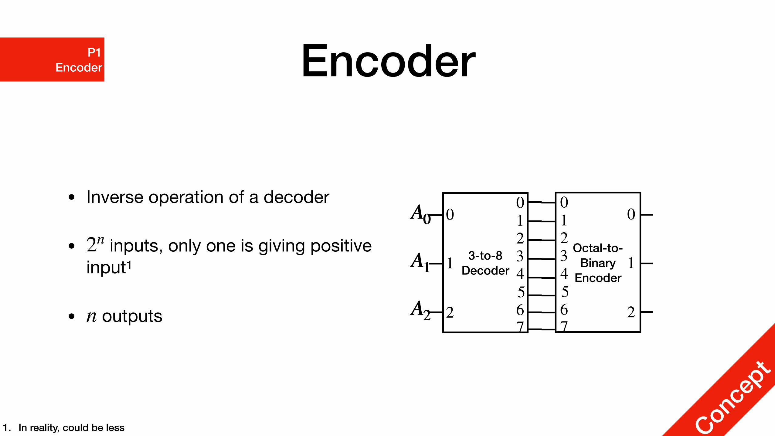
Encoder
• Inverse operation of a decoder
• inputs, only one is giving positive input1
• outputs
2n
n
Concep
t
P1 Encoder
1. In reality, could be less
3-to-8 Decoder
01234567
0
1
2
Octal-to-Binary
Encoder
01234567
0
1
2
Encoder
• Inverse operation of a decoder
• inputs, only one is giving positive input1
• outputs
2n
n
Concep
t
P1 Encoder
1. In reality, could be less
A0
A1
A2
A0
A1
A2
3-to-8 Decoder
01234567
0
1
2
Octal-to-Binary
Encoder
01234567
0
1
2

EncoderP1 Encoder
Octal-to-Binary
Encoder
01234567
0
1
2
D7 D6 D5 D4 D3 D2 D1 D0 A2 A1 A0
1 0 0 0
1 0 0 1
1 0 1 0
1 0 1 1
1 1 0 0
1 1 0 1
1 1 1 0
1 1 1 1
Concep
t
A0 = D1 + D3 + D5 + D7
A1 = D2 + D3 + D6 + D7
A2 = D4 + D5 + D6 + D7

Encoder
• What happens if the inputs are all 0s?
• What happens if the inputs include multiple 1s?
P1 Encoder
Octal-to-Binary
Encoder
01234567
0
1
2
A0 = D1 + D3 + D5 + D7
A1 = D2 + D3 + D6 + D7
A2 = D4 + D5 + D6 + D7
Concep
t

Priority Encoder
• Additional Validity Output
• Indicating whether the input is valid (contains 1)
• Priority
• Ignores if
V
D<i Di = 1
P1 Encoder
Concep
t
Priority Encoder
0
1
2
3
0
1
V

Priority EncoderP1 Encoder
Priority Encoder
0
1
2
3
0
1
V
Concep
t
D3 D2 D1 D0 A1 A0 V
0 0 0 0 X X 0
0 0 0 1 0 0 1
0 0 1 X 0 1 1
0 1 X X 1 0 1
1 X X X 1 1 1
0
X
X
X
X
XX

Priority EncoderP1 Encoder
Priority Encoder
0
1
2
3
0
1
V
Concep
t
D3 D2 D1 D0 A1 A0 V
0 0 0 0 0 0 0
0 0 0 1 0 0 1
0 0 1 X 0 1 1
0 1 X X 1 0 1
1 X X X 1 1 1
V = D3 + D2 + D1 + D0
A1 = D3 + D3D2 = D2 + D3
A0 = D3D2D1 + D3
= D2D1 + D3

Multiplexer
Summary
P2 Multiplexer
Switch Modes

Multiplexer
• Multiple -variable input vectors
• Single -variable output vector
• Switches: which input vectors to output
n
n
Concep
t
P2 Multiplexer
n
n
…
n
n

Single-Bit 2-to-1 Multiplexer
• 2 single-bit inputs
• 1 single-bit output
• 1-bit switch
Concep
t
P2 Multiplexer
01
I0
I1
S
Y

Single-Bit 2-to-1 Multiplexer
Concep
t
P2 Multiplexer
01
I0
I1
S
Y
S I0 I1 Y
0 0 X 0
0 1 X 1
1 X 0 0
1 X 1 1

Single-Bit 2-to-1 Multiplexer
Concep
t
P2 Multiplexer
01
I0
I1
S
Y
3-7 / Selecting 141
This same equation can be obtained by using a 3-variable K-map. As shown in Figure 3-24(a), the implementation of the preceding equation can be decomposed into a 1–to–2-line decoder, two enabling circuits, and a 2-input OR gate. A common symbol for a 2-to-1 multiplexer is shown in Figure 3-24(b), with a trapezoid signify-ing the selection of the output on the short parallel side from among the 2n informa-tion inputs on the long parallel side.
Suppose that we wish to design a 4–to–1-line multiplexer. In this case, the function Y depends on four inputs I0, I1, I2, and I3 and two select inputs S1 and S0. By placing the values of I0 through I3 in the Y column, we can form Table 3-8, a condensed truth table for this multiplexer. In this table, the information variables do not appear as input columns of the table but appear in the output column. Each row represents multiple rows of the full truth table. In Table 3-8, the row 00 I0 represents all rows in which (S1, S0) = 00. For I0 = 1 it gives Y = 1, and for I0 = 0 it gives Y = 0. Since there are six variables, and only S1 and S0 are !xed, this single row represents 16 rows of the corresponding full truth table. From the table, we can write the equation for Y as
Y = S1S0 I0 + S1S0 I1 + S1S0 I2 + S1S0 I3
If this equation is implemented directly, two inverters, four 3-input AND gates, and a 4-input OR gate are required, giving a gate-input cost of 18. A different imple-mentation can be obtained by factoring the AND terms to give
Y = (S1S0)I0 + (S1S0)I1 + (S1S0)I2 + (S1S0)I3
FIGURE 3-24(a) Single-Bit 2–to–1-Line Multiplexer; (b) common Symbol for a Multiplexer
TABLE 3-8Condensed Truth Table for 4-to-1-Line Multiplexer
S1 S0 Y
0 0 I 00 1 I 11 0 I 21 1 I 3
Y
Y
S
S
DecoderEnablingCircuits I0 0
1I1
I0
I1
(b)(a)
M03_MANO0637_05_SE_C03.indd 141 23/01/15 1:51 PM
Technology• 1 x 1-to-2 Decoder• 2 x 1-bit Enabler• 1 x 2-input OR Gate

Single-Bit 4-to-1 Multiplexer
Concep
t
P2 Multiplexer
0
3
12
2
I0
I3
S(1:0)
YI1I2
Technology• 1 x 2-to-4 Decoder• 4 x 1-bit Enabler• 1 x 4-input OR Gate
YS
DecoderEnablingCircuits
I0
I1

Single-Bit 4-to-1 Multiplexer
Concep
t
P2 Multiplexer
0
3
12
2
I0
I3
S(1:0)
YI1I2
Technology• 1 x 2-to-4 Decoder• 4 x 1-bit Enabler• 1 x 4-input OR Gate
142 CHAPTER 3 / COMBINATIONAL LOGIC DESIGN
This implementation can be constructed by combining a 2–to–4-line decoder, four AND gates used as enabling circuits, and a 4-input OR gate, as shown in Figure 3-25. We will refer to the combination of AND gates and OR gates as an m * 2 AND-OR, where m is the number of AND gates and 2 is the number of inputs to the AND gates. This resulting circuit has a gate input cost of 22, which is more costly. Nevertheless, it provides a structural basis for construct-ing larger n–to–2n-line multiplexers by expansion.
A multiplexer is also called a data selector, since it selects one of many infor-mation inputs and steers the binary information to the output line. The term “multi-plexer” is often abbreviated as “MUX.”
Multiplexers can be expanded by considering vectors of input bits for larger values of n. Expansion is based upon the circuit structure given in Figure 3-24(a), consisting of a decoder, enabling circuits, and an OR gate. Multiplexer design is illus-trated in Examples 3-10 and 3-11.
EXAMPLE 3-10 64–to–1-Line Multiplexer
A multiplexer is to be designed for n = 6. This will require a 6–to–64-line decoder as given in Figure 3-15, and a 64 * 2 AND-OR gate. The resulting structure is shown in Figure 3-26. This structure has a gate-input cost of 182 + 128 + 64 = 374.
In contrast, if the decoder and the enabling circuit were replaced by invert-ers plus 7-input AND gates, the gate-input cost would be 6 + 448 + 64 = 518. For single-bit multiplexers such as this one, combining the AND gate generating Di with the AND gate driven by Di into a single 3-input AND gate for every i = 0 through 63 reduces the gate-input cost to 310. For multiple-bit multiplexers, this
S1Decoder
S0
I0
I1Y
I2
I3
FIGURE 3-25A Single-Bit 4–to–1-Line Multiplexer
M03_MANO0637_05_SE_C03.indd 142 23/01/15 1:51 PM

Circuit Drawing Time!
Summary
P3 LogicWorks
It’s OK, this is the last time…Sorta…

Last Circuit Drawing Practice
1. Sub-circuit
2. Implementing 2-to-4 Decoder using drawing tools
3. Implementing 3-to-8 Decoder using 2-to-4 Decoders
4. Implementing Octal-to-Binary Priority Encoder using drawing tools1
5. Implementing 4bit 4-to-1 Multiplexer using drawing 3-to-8 Decoder1
Concep
t
P3 LogicWorks
1. You will be reusing these designs in later lectures and assignments

Sub-circuit
Tech
nical
P3 LogicWorks
1. Implement an enabler, then select the Pseudo Devices library

Sub-circuit
Tech
nical
P3 LogicWorks
2. Replace the switch with Port In, replace the probs with Port Out
…

Sub-circuit
Tech
nical
P3 LogicWorks
2. Replace the switch with Port In, replace the probs with Port Out
…

Sub-circuit
Tech
nical
P3 LogicWorks
3. File-New-Device Symbol

Sub-circuit
1. Sub-circuit
2. Implementing 2-to-4 Decoder using drawing tools
3. Implementing 3-to-8 Decoder 2-to-4 Decoders
4. Implementing Octal-to-Binary Priority Encoder using drawing tools1
5. Implementing Multiplexer using drawing tools1
Tech
nical
P3 LogicWorks
4. With the Circuit.cct open and Part1 open, go to Options — Subcircuit and Part Type

Sub-circuit
Tech
nical
P3 LogicWorks
5. Select Create a subcircuit symbol and select an open circuit to attach to it

Sub-circuit
Tech
nical
P3 LogicWorks
6. Select Circuit.cct

Sub-circuit
Tech
nical
P3 LogicWorks
7. Draw a rectangle and add the THIN pins
Use these pins only!
Add a text description

Sub-circuit
Tech
nical
P3 LogicWorks
8. Save the part in a new library, e.g. CSCI150

Sub-circuit
Tech
nical
P3 LogicWorks
9. Now you are a much happier person

Last Circuit Drawing Practice
1. Sub-circuit
2. Implementing 2-to-4 Decoder using drawing tools
3. Implementing 3-to-8 Decoder using 2-to-4 Decoders
4. Implementing Octal-to-Binary Priority Encoder using drawing tools1
5. Implementing 4bit 4-to-1 Multiplexer using drawing 3-to-8 Decoder1
Concep
t
P3 LogicWorks
1. You will be reusing these designs in later lectures and assignments