03nano English
5
Nano science and technology and its applications Dr. Jian WANG Department of Physics, The University of Hong Kong What is nano science and technology? Nano is an abbreviation of nanometer (nm) which is a unit of length. It is one billionth of a meter, a very small length indeed. The diameter of human's hair is about sixty thousand to eighty thousand nanometers. If we could put hydrogen atoms together, one nanometer would approximately equal to the length of ten hydrogen atoms that put together in a line. A material is called the nano- material if the size of the material is below 100 nm. You may wonder why 100 nm but not 1000 nm or 10 nm? This is because many physical and chemical properties of the material change significantly when its size is below 100 nm. For instance, the surface effect will play a major role for nano-material. Suppose we have a cube with side a, the surface area is 6*a*a. If we divide it int o ei gh t (2*2* 2) smalle r cubes eac h wi th sid e a/ 2, the n the to tal sur face area is 8*6*(a/2)*(a/2)=12*a*a. In general, we can divide it into N*N*N smaller cubes each with side a/N, the total surface area is N*6*a*a. We conclude that the smaller the cubes, the larger the total surface area to volume ratio. Therefore if we have a gram of gold grains whose size is below 100 nm the surface of the grain will become very important. We know that the atoms on the material surface are highly unstable and very active in the chemical reaction. As a result, the increasing of the surface area will greatly enhance the chemical reaction, the ability of surface absorption, and the cata lyt ic ability of the mate ria l. In addit ion, the abil ity of heat conduct ion, mec hani cal strength, as well as optical property of the nano-materials are also very different from that of bulk system. For example, the melting point of metal gold is about 1000 o C whereas for the nano sized gold grains with typical size of 2 nm, the melting point is down to 330 C ° . The absorption of ultra vio let of some nano mater ials can be enhanc ed significantly. Furthermore, new effects start to manifest when the size is below 100 nm. Hence a class of new materials emerges at nano scale. Can we make nano-sized material? Can we create new materials using clusters of molecules or atoms as building blocks? The answer is yes. Such nano-technology exist now and due to its advance the nano-science becomes possible. To move atoms individually has been the dream of scientists for a long time. The Nobel laureate Richard Feynman said in 1959 "The problems of chemistry and biology can be greatly helped if our ability to see what we are doing, and to do things on an atomic level, is ultimately developed --- a development which I think cannot be avoided." Indeed, one can manipulate atoms now using Scanning tunneling microscope (STM). A STM is a device for imaging surfaces of materials with very high magnification, down to atomic scale. Using STM one can create various exciting atomic structures (see Fig.1: Xenon on Nickel). The invention of STM is really revolutionary and essential for the study of nano science. Because of this it won the Nobel Prize in physics in 1986.
-
Upload
preet-kaur -
Category
Documents
-
view
217 -
download
0
Transcript of 03nano English
8/6/2019 03nano English
http://slidepdf.com/reader/full/03nano-english 1/5
Nano science and technology and its applications
Dr. Jian WANG Department of Physics, The University of Hong Kong
What is nano science and technology?
Nano is an abbreviation of nanometer (nm) which is a unit of length. It is one billionth of a meter,a very small length indeed. The diameter of human's hair is about sixty thousand to eighty thousandnanometers. If we could put hydrogen atoms together, one nanometer would approximately equalto the length of ten hydrogen atoms that put together in a line. A material is called the nano-material if the size of the material is below 100 nm. You may wonder why 100 nm but not 1000nm or 10 nm? This is because many physical and chemical properties of the material changesignificantly when its size is below 100 nm. For instance, the surface effect will play a major rolefor nano-material. Suppose we have a cube with side a, the surface area is 6*a*a. If we divide it
into eight (2*2*2) smaller cubes each with side a/2, then the total surface area is8*6*(a/2)*(a/2)=12*a*a. In general, we can divide it into N*N*N smaller cubes each with sidea/N, the total surface area is N*6*a*a. We conclude that the smaller the cubes, the larger the totalsurface area to volume ratio. Therefore if we have a gram of gold grains whose size is below 100nm the surface of the grain will become very important. We know that the atoms on the materialsurface are highly unstable and very active in the chemical reaction. As a result, the increasing of the surface area will greatly enhance the chemical reaction, the ability of surface absorption, andthe catalytic ability of the material. In addition, the ability of heat conduction, mechanicalstrength, as well as optical property of the nano-materials are also very different from that of bulk system. For example, the melting point of metal gold is about 1000 oC whereas for the nano sizedgold grains with typical size of 2 nm, the melting point is down to 330 C ° . The absorption of ultra
violet of some nano materials can be enhanced significantly. Furthermore, new effects start tomanifest when the size is below 100 nm. Hence a class of new materials emerges at nano scale.
Can we make nano-sized material? Can we create new materials using clusters of molecules or atoms as building blocks? The answer is yes. Such nano-technology exist now and due to itsadvance the nano-science becomes possible. To move atoms individually has been the dream of scientists for a long time. The Nobel laureate Richard Feynman said in 1959 "The problems of chemistry and biology can be greatly helped if our ability to see what we are doing, and to dothings on an atomic level, is ultimately developed --- a development which I think cannot beavoided." Indeed, one can manipulate atoms now using Scanning tunneling microscope (STM). ASTM is a device for imaging surfaces of materials with very high magnification, down to atomicscale. Using STM one can create various exciting atomic structures (see Fig.1: Xenon on Nickel).
The invention of STM is really revolutionary and essential for the study of nano science. Becauseof this it won the Nobel Prize in physics in 1986.
8/6/2019 03nano English
http://slidepdf.com/reader/full/03nano-english 2/5
Figure 1.Fig.1 is from http://www.almaden.ibm.com/vis/stm/atomo.html.
Besides the interest from the fundamental science, another driving force of nano science is of course the potential device applications. We know that many of our daily electrical appliancesconsist of transistors as basic components. The first transistor is made in 1941 whose size is about
one cubic cm. The scientist who invented the transistor later won the Nobel Prize in physics in1956. Due to the advance of modern technology, the size of transistor that one can make becomessmaller and smaller. Consequently, the number of transistors that can be put in a computer chipdoubles in every 18 months. This is so called Moore's law. In 1991, a computer chip of size onecubic cm contains about three million transistors. According to Moore's law, the dimension of thetransistor in the computer chip will reach 130 nm in the near future. In such a small length scale, previous traditional technology of fabricating transistor can no longer be used. New nanotechnology has to be developed. More importantly, new physical laws will emerge in such a smalldimension.
Why nano science: it offers one of the most exciting prospects for new phenomena, new materials,and new science. Some people believe that it will lead to a new industrial revolution. Roughlyspeaking, the nano technology has been applied to the four disciplines: (1). nano electronics: newelectronic devices with novel functions and the advantage of high speed and at the same timeconsuming less energy power. (2). nano material science: new materials with novel properties,which grow perfectly without any impurities and defects, ideal for nano devices. (3). nano biologyincluding mapping the genetic information in DNA and RNA molecules. (4). nano medicine:discover, design, and deliver new drugs on nano level.
Currently the nano science and technology has been a "hot" project in many countries who investtremendous amount of money. For instance, in early 2000 United States former president Clintonannounced the "national nano technology initiative" and put in 225 million US dollars for this plan.In 2001, the amount of research funding doubles. In Japan, the nano science and technology is one
of the four key areas of future development with total research grant over 380 million US dollars.In Europe, the five-year plan for nano science and technology (99-03) in ongoing. In China, hugeamount of research grants are available for nano science.
The application of nano science and technology has a huge market worldwide with market valueover 50 billion US dollars in 2000, most of it is in the application of nano materials. Germany predicted that the market value in the year 2010 will be over 1 trillion US dollars. People believethat the application of nano biology and nano medicine will have a breakthrough in the near future.
8/6/2019 03nano English
http://slidepdf.com/reader/full/03nano-english 3/5
However, for the full application of nano electronics, which is the most important area in nanoscience and technology, we probably have to wait for some 20 years.
Carbon nanotubes and its application
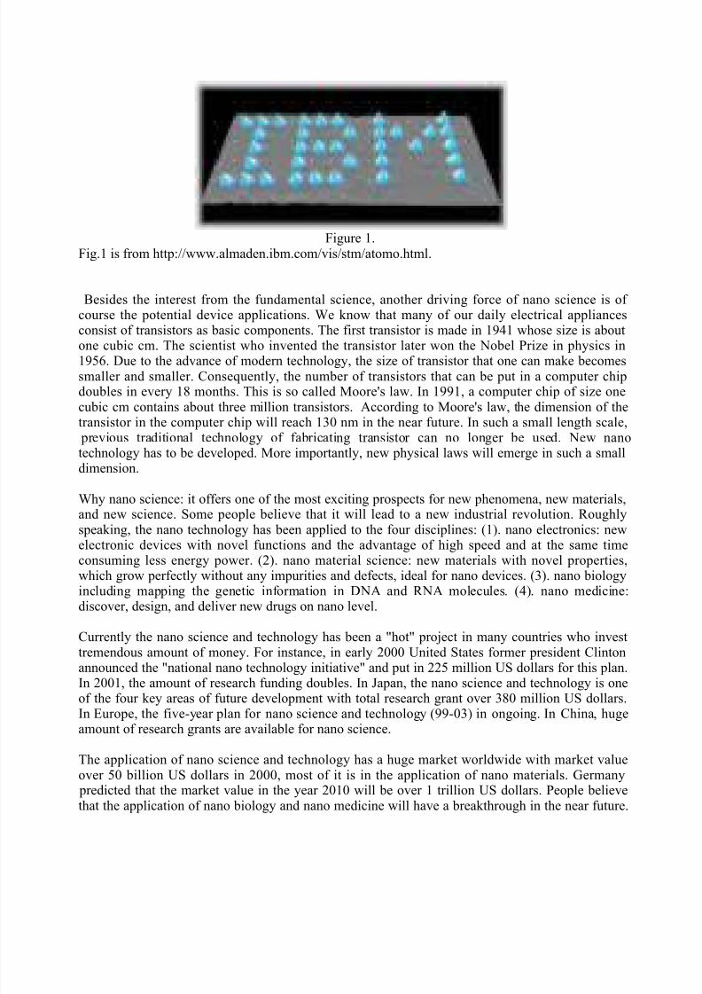
One of the examples of nano-materials is the Carbon nanotube: a man-made nano-material whichcan not be found in nature. It has many interesting physical and chemical properties and many of them have great potential device application. There are four kinds of structure made of Carbon: (1).diamond structure. (2). graphite (honeycomb) structure: pencil lead. (3). Carbon 60: Buckyball (itsdiscovery won 1996 Nobel Prize in chemistry). (4). Carbon nanotube (CNT): by rolling up agraphite sheet (see Fig.2) as a cylinder like a straw. Different ways of rolling the graphite sheetgive different kinds of CNT: armchair nanotube, zigzag nanotube, and chiral nanotube. For instance, connecting the coordinates (0,0) and (5,5) gives an armchair structure denoted as (5,5);connecting (0,0) and (9,0) gives a zigzag structure (9,0); connecting (0,0) and (6,2) gives chiralstructure (6,2). The first CNT was discovered by a Japanese scientist Iijima in 1991. The smallestCNT in the world has been made in 2001 at The Hong Kong University of Science and Technology
by a group of physicists. The diameter is around 0.4 nm. Depending on different ways of rolling,CNT could be good or poor conductor. It has very good mechanical properties as well. For instance, it is about 100 time stronger than steel with only one sixth of the weight. They can sustainlarge force without breaking up. The scientists are exploring ways to blend CNTs with plastics andceramics to produce new composites with unprecedented strength to weight ratios and highconductivity. For example, it is found that by adding one to five percent of CNT into epoxy resin,the hardness will be increased by three-fold.
Figure 2a. Figure 2b.
Other applications of nano-science
(1). A new ceramics (or porcelain) material. As is well known that the traditional ceramics is very brittle with poor tenacity and strength. The ceramics made of nano sized material has highhardness and good tenacity. One can even make a spring from the new ceramics material. Hardto believe, isn't it?
8/6/2019 03nano English
http://slidepdf.com/reader/full/03nano-english 4/5
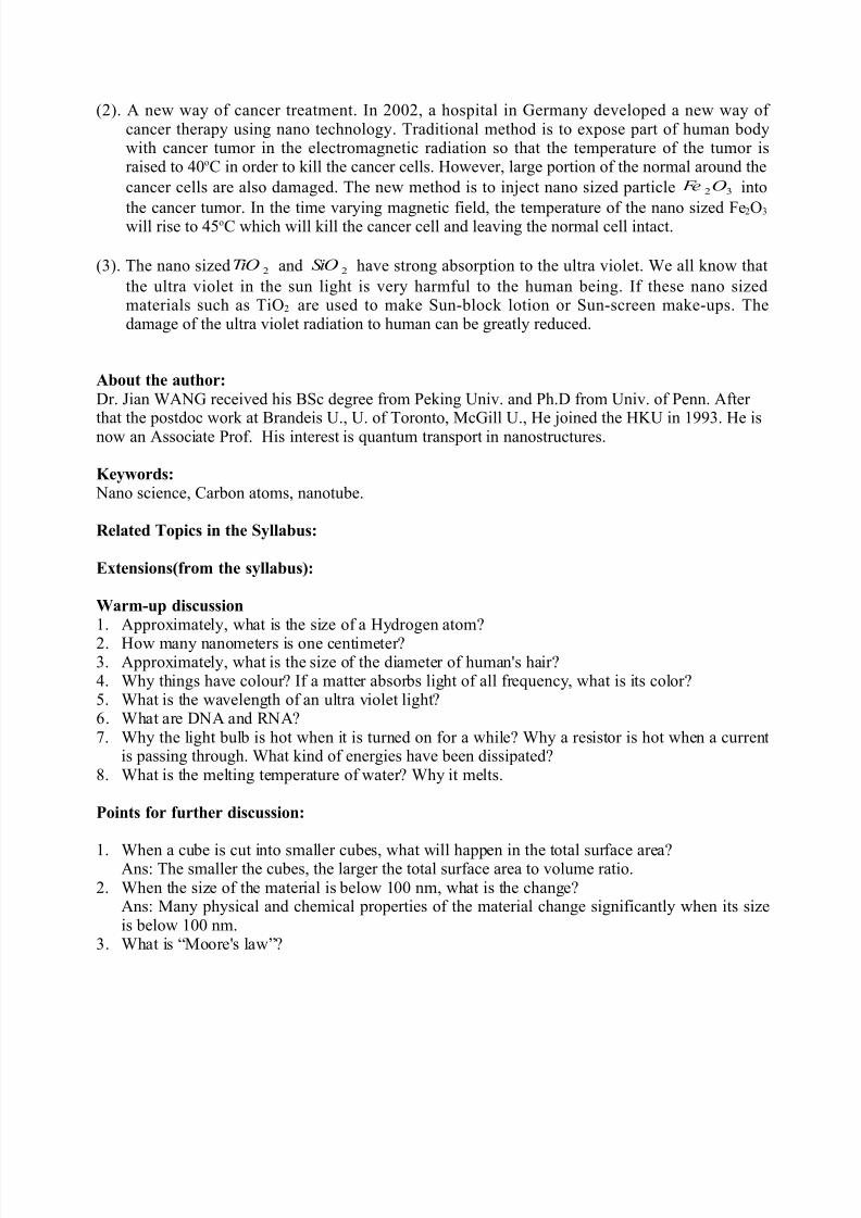
(2). A new way of cancer treatment. In 2002, a hospital in Germany developed a new way of cancer therapy using nano technology. Traditional method is to expose part of human bodywith cancer tumor in the electromagnetic radiation so that the temperature of the tumor israised to 40oC in order to kill the cancer cells. However, large portion of the normal around the
cancer cells are also damaged. The new method is to inject nano sized particle 32O Fe into
the cancer tumor. In the time varying magnetic field, the temperature of the nano sized Fe 2O3
will rise to 45oC which will kill the cancer cell and leaving the normal cell intact.
(3). The nano sized 2TiO and 2
SiO have strong absorption to the ultra violet. We all know that
the ultra violet in the sun light is very harmful to the human being. If these nano sizedmaterials such as TiO2 are used to make Sun-block lotion or Sun-screen make-ups. Thedamage of the ultra violet radiation to human can be greatly reduced.
About the author:
Dr. Jian WANG received his BSc degree from Peking Univ. and Ph.D from Univ. of Penn. After that the postdoc work at Brandeis U., U. of Toronto, McGill U., He joined the HKU in 1993. He isnow an Associate Prof. His interest is quantum transport in nanostructures.
Keywords: Nano science, Carbon atoms, nanotube.
Related Topics in the Syllabus:
Extensions(from the syllabus):
Warm-up discussion1. Approximately, what is the size of a Hydrogen atom?
2. How many nanometers is one centimeter?3. Approximately, what is the size of the diameter of human's hair?4. Why things have colour? If a matter absorbs light of all frequency, what is its color?5. What is the wavelength of an ultra violet light?6. What are DNA and RNA?7. Why the light bulb is hot when it is turned on for a while? Why a resistor is hot when a current
is passing through. What kind of energies have been dissipated?8. What is the melting temperature of water? Why it melts.
Points for further discussion:
1. When a cube is cut into smaller cubes, what will happen in the total surface area?Ans: The smaller the cubes, the larger the total surface area to volume ratio.
2. When the size of the material is below 100 nm, what is the change?Ans: Many physical and chemical properties of the material change significantly when its sizeis below 100 nm.
3. What is “Moore's law”?
8/6/2019 03nano English
http://slidepdf.com/reader/full/03nano-english 5/5
Ans: Due to the advance of modern technology, the size of transistor that one can make becomes smaller and smaller. Consequently, the number of transistors that can be put in acomputer chip doubles in every 18 months. This is so called Moore's law.
Activities:1. By rolling a graphite sheet to make a nanotube.2. Can you imagine some applications of nanotube?
Related web sites:
Carbon nanotube science and technologyhttp://www.personal.rdg.ac.uk/~scsharip/tubes.htm
The Nanotube SiteThis site contains information and some hyperlinks about nanotube technology.http://www.pa.msu.edu/cmp/csc/nanotube.html
Scientific American (Taiwan version)--- Nano-technology (Chinese version only)This site contains two articles about the development of education in nano-technology.http://www.sciam.com.tw/special/special.asp
Scientific American---The Nanodrive Project (In brief)Inventing a nanotechnology device for mass production and consumer use is trickier than itsounds.http://www.sciam.com/article.cfm?chanID=sa006&colID=1&articleID=000CCFEC-C4F4-1DF7-9733809EC588EEDF
IBM Research---Nanotechnology
This site contains latest research development of IBM in nanotechnology.http://www.research.ibm.com/pics/nanotech/
Scientific American---Application of nanotechnology in medicine (Chinese version only) New nanotechnology will be applied in biological and medical fields.http://www.sciam.com.tw/read/readshow.asp?FDocNo=121&CL=18
Further readings:
References:


![...(EPUU) 21 I English IA] r Integrated English rintegrated English 101), rintegrated English 11 I I Is English IJ e. UT, rAdvanced English 11], English 111] r Integrated English Study](https://static.fdocuments.us/doc/165x107/5f9c0b33f8367823672ad80f/-epuu-21-i-english-ia-r-integrated-english-rintegrated-english-101-rintegrated.jpg)