0 Hz/dc to 14 GHz, Single-Pole, Four-Throw MEMS Switch ... · 0 Hz/dc to 14 GHz, Single-Pole,...
33
0 Hz/dc to 14 GHz, Single-Pole, Four-Throw MEMS Switch with Integrated Driver Data Sheet ADGM1304 Rev. F Document Feedback Information furnished by Analog Devices is believed to be accurate and reliable. However, no responsibility is assumed by Analog Devices for its use, nor for any infringements of patents or other rights of third parties that may result from its use. Specifications subject to change without notice. No license is granted by implication or otherwise under any patent or patent rights of Analog Devices. Trademarks and registered trademarks are the property of their respective owners. One Technology Way, P.O. Box 9106, Norwood, MA 02062-9106, U.S.A. Tel: 781.329.4700 ©2016–2020 Analog Devices, Inc. All rights reserved. Technical Support www.analog.com FEATURES Fully operational down to 0 Hz/dc On resistance: 2.9 Ω (maximum) Off leakage: 0.5 nA (maximum) −3 dB bandwidth 11 GHz (typical) for RF1, RF4 14 GHz (typical) for RF2, RF3 RF performance characteristics Insertion loss: 0.26 dB (typical) at 2.5 GHz Isolation: 24 dB (typical) at 2.5 GHz IIP3: 69 dBm (typical) RF power: 36 dBm (maximum) Actuation lifetime: 1 billion cycles (minimum) Hermetically sealed switch contacts On switching time: 75 µs (maximum) Integrated driver removes the need for an external driver Supply voltage: 3.0 V to 3.6 V CMOS-/LVTTL-compatible Parallel and SPI interface Independently controllable switches Switch is in an open state with no power supply present Requirement to mitigate floating nodes on all RF pins, see the Floating Node section 24-lead, 5 mm × 4 mm × 0.95 mm, LFCSP Operating temperature range: 0°C to 85°C APPLICATIONS Relay replacements Automatic test equipment: RF/high speed digital and mixed signals Load and probe boards: RF/high speed digital and mixed signals RF test instrumentation Reconfigurable filters and attenuators High performance RF switching GENERAL DESCRIPTION The ADGM1304 is a wideband, single-pole, four-throw (SP4T) switch, fabricated using Analog Devices, Inc., microelectro- mechanical system (MEMS) switch technology. This technology enables a small form factor, wide RF bandwidth, highly linear, low insertion loss switch that is operational from 0 Hz/dc to 14 GHz, making the ADGM1304 an ideal solution for a wide range of RF and precision equipment switching needs. An integrated driver chip generates a high voltage to electro- statically actuate a switch that can be controlled by a parallel interface and a serial peripheral interface (SPI). All four switches are independently controllable. The device is packaged in a 24-lead, 5 mm × 4 mm × 0.95 mm, lead frame chip-scale package (LFCSP). To ensure optimum operation of the ADGM1304, the Critical Operational Requirements section must be followed exactly. The on resistance (RON) performance of the ADGM1304 is affected by device to device variation, channel to channel variation, cycle actuations, settling time post turn on, bias voltage, and temperature changes.
Transcript of 0 Hz/dc to 14 GHz, Single-Pole, Four-Throw MEMS Switch ... · 0 Hz/dc to 14 GHz, Single-Pole,...

0 Hz/dc to 14 GHz, Single-Pole, Four-Throw MEMS Switch with Integrated Driver
Data Sheet ADGM1304
Rev. F Document Feedback Information furnished by Analog Devices is believed to be accurate and reliable. However, no responsibility is assumed by Analog Devices for its use, nor for any infringements of patents or other rights of third parties that may result from its use. Specifications subject to change without notice. No license is granted by implication or otherwise under any patent or patent rights of Analog Devices. Trademarks and registered trademarks are the property of their respective owners.
One Technology Way, P.O. Box 9106, Norwood, MA 02062-9106, U.S.A. Tel: 781.329.4700 ©2016–2020 Analog Devices, Inc. All rights reserved. Technical Support www.analog.com
FEATURES Fully operational down to 0 Hz/dc
On resistance: 2.9 Ω (maximum) Off leakage: 0.5 nA (maximum)
−3 dB bandwidth 11 GHz (typical) for RF1, RF4 14 GHz (typical) for RF2, RF3
RF performance characteristics Insertion loss: 0.26 dB (typical) at 2.5 GHz Isolation: 24 dB (typical) at 2.5 GHz IIP3: 69 dBm (typical) RF power: 36 dBm (maximum)
Actuation lifetime: 1 billion cycles (minimum) Hermetically sealed switch contacts On switching time: 75 µs (maximum)
Integrated driver removes the need for an external driver Supply voltage: 3.0 V to 3.6 V CMOS-/LVTTL-compatible Parallel and SPI interface Independently controllable switches
Switch is in an open state with no power supply present Requirement to mitigate floating nodes on all RF pins, see
the Floating Node section 24-lead, 5 mm × 4 mm × 0.95 mm, LFCSP Operating temperature range: 0°C to 85°C
APPLICATIONS Relay replacements Automatic test equipment: RF/high speed digital and mixed
signals Load and probe boards: RF/high speed digital and mixed
signals RF test instrumentation Reconfigurable filters and attenuators High performance RF switching
GENERAL DESCRIPTION The ADGM1304 is a wideband, single-pole, four-throw (SP4T) switch, fabricated using Analog Devices, Inc., microelectro-mechanical system (MEMS) switch technology. This technology enables a small form factor, wide RF bandwidth, highly linear, low insertion loss switch that is operational from 0 Hz/dc to 14 GHz, making the ADGM1304 an ideal solution for a wide range of RF and precision equipment switching needs.
An integrated driver chip generates a high voltage to electro-statically actuate a switch that can be controlled by a parallel interface and a serial peripheral interface (SPI). All four switches are independently controllable.
The device is packaged in a 24-lead, 5 mm × 4 mm × 0.95 mm, lead frame chip-scale package (LFCSP).
To ensure optimum operation of the ADGM1304, the Critical Operational Requirements section must be followed exactly.
The on resistance (RON) performance of the ADGM1304 is affected by device to device variation, channel to channel variation, cycle actuations, settling time post turn on, bias voltage, and temperature changes.
ADGM1304 Data Sheet
Rev. F | Page 2 of 33
TABLE OF CONTENTS Features .............................................................................................. 1
Applications ....................................................................................... 1
General Description ......................................................................... 1
Revision History ............................................................................... 2
Functional Block Diagram .............................................................. 4
Specifications ..................................................................................... 5
Timing Characteristics ................................................................ 7
Absolute Maximum Ratings ............................................................ 9
Thermal Resistance ...................................................................... 9
ESD Caution .................................................................................. 9
Pin Configuration and Function Descriptions ........................... 10
Typical Performance Characteristics ........................................... 12
Eye Diagrams .............................................................................. 17
Test Circuits ..................................................................................... 18
Terminology .................................................................................... 21
Theory of Operation ...................................................................... 23
Parallel Digital Interface ............................................................ 23
SPI Digital Interface ................................................................... 24
Internal Oscillator Feedthrough ............................................... 26
Internal Oscillator Feedthrough Mitigation ........................... 26
Low Power Mode ........................................................................ 26
Typical Operating Circuit ......................................................... 26
Applications Information .............................................................. 28
Switchable RF Attenuator .......................................................... 28
Reconfigurable RF Filter ........................................................... 28
Critical Operational Requirements .............................................. 29
System Error Considerations Due to On-Resistance Drift... 29
Floating Node ............................................................................. 29
Cumulative On Switch Lifetime ............................................... 30
Handling Precautions ................................................................ 30
Register Summary and Details ..................................................... 32
Switch Data Register .................................................................. 32
Outline Dimensions ....................................................................... 33
Ordering Guide .......................................................................... 33
REVISION HISTORY 1/2020—Rev. E to Rev. F Changes to Figure 1 .......................................................................... 4 1/2020—Rev. D to Rev. E Reorganized Layout ............................................................ Universal Changes to Features Section and General Description Section ..... 1 Changes to Table 1 ............................................................................ 5 Added Timing Characteristics and Table 2; Renumbered Sequentially ....................................................................................... 7 Added Figure 2 to Figure 4; Renumbered Sequentially ............... 8 Changes to Table 3 ............................................................................ 9 Changes to Figure 5 and Table 5 ................................................... 10 Deleted Figure 7 and Figure 9; Renumbered Sequentially ........ 12 Added Figure 6 to Figure 11 .......................................................... 12 Deleted Figure 14 and Figure 17 ................................................... 13 Added Figure 12 to Figure 14 ........................................................ 13 Added Figure 19 .............................................................................. 14 Added Figure 26 to Figure 29 ........................................................ 15 Added Figure 30 to Figure 32 ........................................................ 16 Deleted Figure 33 and Figure 36 ................................................... 17 Changes to Figure 40 ...................................................................... 18 Deleted Figure 43 and Figure 45 ................................................... 19 Added Figure 43 .............................................................................. 19 Added Figure 46 and Figure 47..................................................... 20 Changes to Terminology Section.................................................. 21 Deleted Sleep Mode (SLEEP) Section .......................................... 23
Changes to Parallel Digital Interface Section ............................. 23 Deleted Driver IC Oscillator Section ........................................... 24 Added SPI Digital Interface Section, Addressable Mode Section, and Daisy-Chain Mode Section ................................................... 24 Changes to Table 6 .......................................................................... 24 Added Figure 50 to Figure 53, Hardware Reset Section, and Internal Error Reset Status Section .............................................. 25 Deleted External Clock (EXTCLK) Section ............................... 26 Added Internal Oscillator Feedthrough Section, Internal Oscillator Feedthrough Mitigation Section, and Low Power Mode Section .................................................................................. 26 Changes to Typical Operating Circuit Section ........................... 26 Changes to Figure 54 ...................................................................... 27 Deleted Floating Node Avoidance Section ................................. 28 Deleted Suggested Application Circuits Section Heading ........ 29 Added Critical Operational Requirements Section, System Error Considerations Due to On-Resistance Drift Section, Table 7, and Floating Node Section ............................................. 29 Deleted ESD Precautions Section and Voltage Standoff Limit Section .............................................................................................. 30 Changes to Figure 63, Figure 64, Cumulative On Switch Lifetime Section, and Electrical Overstress (EOS) Precautions Section .............................................................................................. 30 Changes to Mechanical Shock Precautions Section and Figure 67 .......................................................................................... 31

Data Sheet ADGM1304
Rev. F | Page 3 of 33
Added Register Summary and Details Section, Table 9, Switch Data Register Section, and Table 10 .............................................. 32 Changes to Ordering Guide ........................................................... 33 3/2018—Rev. C to Rev. D Changes to Features Section ............................................................ 1 Changes to On Resistance Parameter and On Leakage Parameter, Table 1 ................................................................................................. 3 Added Endnote 6, Table 1; Renumbered Sequentially ................. 4 Changes to Figure 11 and Figure 14 ............................................... 8 Added Eye Diagrams Section and Figure 17 to Figure 22; Renumbered Sequentially .............................................................. 10 Added Figure 30, Figure 31, and Figure 32 .................................. 12 Changes to Floating Node Avoidance Section, Figure 36, and Figure 40 ........................................................................................... 18 Changes to Ordering Guide ........................................................... 22 10/2016—Revision C: Initial Version
ADGM1304 Data Sheet
Rev. F | Page 4 of 33
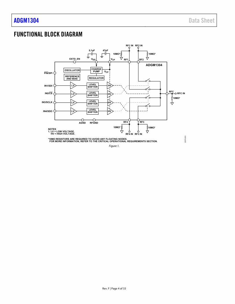
FUNCTIONAL BLOCK DIAGRAM
CHARGEPUMP
VCP
VCP
VDD
RFGND
OSCILLATOR
EXTD_EN
REGULATOR REFERENCE
AND BIAS
LEVELSHIFTER
LEVELSHIFTER
LEVELSHIFTER
LEVELSHIFTER
RF3RF4
RF1 RF2
ADGM1304
RFC
NOTES1. LV = LOW VOLTAGE. HV = HIGH VOLTAGE.
AGND
HV
HV
LV
LV
LV
LV
1287
4-00
1
HV
HV
RF2 INRF1 IN
RF4 IN RF3 IN
10MΩ* 10MΩ*
10MΩ*
10MΩ* 10MΩ*
RFC IN
47pF0.1µF
IN1/SDI
IN2/CS
IN3/SCLK
IN4/SDO
PIN/SPI
*10MΩ RESISTORS ARE REQUIRED TO AVOID ANY FLOATING NODES. FOR MORE INFORMATION, REFER TO THE CRITICAL OPERATIONAL REQUIREMENTS SECTION.
Figure 1.

Data Sheet ADGM1304
Rev. F | Page 5 of 33
SPECIFICATIONS VDD = 3.0 V to 3.6, AGND = 0 V, RFGND = 0 V, all specifications minimum temperature (TMIN) to maximum temperature (TMAX) = 0°C to 85°C, unless otherwise noted.
Table 1. Parameter Symbol Min Typ1 Max Unit Test Conditions/Comments2
ON-RESISTANCE PROPERTIES See Figure 6 to Figure 13 for more details Initial On-Resistance
Properties
On Resistance RON 2.9 Ω Drain source current (IDS) = 50 mA, 0 V input bias, at 1 ms after first actuation
On-Resistance Match Between Channels
ΔRON CH_CH 1 Ω
On-Resistance Drift Over Time3 ΔRON TIME −0.25 Ω RON changed from 1 ms to 100 ms after first actuation Over Actuations4 ΔRON 0.5 Ω 109 actuations, switch is actuated at 25°C and RON is
measured at 25°C 5 Ω 109 actuations, switch is actuated at 85°C and RON is measured
at 25°C, 1 kHz actuating frequency, 220 mA load applied between toggles5
RELIABILITY PROPERTIES
Continuously On Lifetime 7.2 Years Median time before failure at 50°C6, see Figure 65 for more details
Actuation Lifetime
Cold Switched 109 Actuations Load between toggling is 220 mA, tested at 85°C
Hot Switched RF power = continuous wave, terminated into 50 Ω, see Figure 14 for details
10 dBm 5.16 × 10⁹ Actuations 50% of test population failure point (T50)
15 dBm 3.21 × 10⁶ Actuations 50% of test population failure point (T50)
20 dBm 390 × 103 Actuations 50% of test population failure point (T50)
DYNAMIC CHARACTERISTICS Operating Frequency 0 Hz/dc 14 GHz Operating frequency −3 dB Bandwidth BW
RF1, RF4 9.3 11 GHz RF1 to RFC and RF4 to RFC channels RF2, RF3 12 14 GHz RF2 to RFC and RF3 to RFC channels
Insertion Loss IL 0.26 0.55 dB At 2.5 GHz, RFC to RFx 0.4 0.9 dB At 6.0 GHz, RFC to RFx Isolation ISO
RFx To RFC (All Off) 23 24 dB At 2.5 GHz, RFx to RFC (all channels off) 16 19 dB At 6.0 GHz, RFx to RFC (all channels off) RF1 to RFC 25 At 6 GHz, RF2 to RFC is on, RF1 to RFC is off RF2 to RFC 23 At 6 GHz, RF1 to RFC is on, RF2 to RFC is off
Crosstalk CTK 27 30 dB At 2.5 GHz, RFx to RFx 22 24 dB At 6.0 GHz, RFx to RFx Return Loss RL 13 18 dB DC to 6.0 GHz Input Third-Order
Intermodulation Intercept IP3 69 dBm Input: 900 MHz and 901 MHz, input power = 27 dBm
Input Second-Order Intermodulation Intercept
IP2 111 dBm Input: 900 MHz and 901 MHz, input power = 27 dBm
Second Harmonic HD2 −90 dBc Input: 5.4 MHz, input power = 0 dBm −85 dBc Input: 150 MHz and 800 MHz, input power = 27 dBm Third Harmonic HD3 −85 dBc Input: 150 MHz and 800 MHz, input power = 27 dBm Total Harmonic Distortion
Plus Noise THD + N −110 dBc Load resistance (RL) = 300 Ω, f = 1 kHz, RFx = 2.5 V p-p
Maximum RF Power 36 dBm Switch in the on state and terminated into 50 Ω, maximum specification tested at 25°C
DC Voltage Range −6 +6 V On switch dc voltage operation range On Switching Time7 tON 0 75 μs 50% INx to 90% (0.05 dB of final IL value) RFx, 50 Ω termination
Off Switching Time7 tOFF 0 75 μs 50% INx to 10% (0.05 dB of final IL value) RFx, 50 Ω termination Actuation Frequency 5 kHz All switches toggled simultaneously
ADGM1304 Data Sheet
Rev. F | Page 6 of 33
Parameter Symbol Min Typ1 Max Unit Test Conditions/Comments2
Power-Up Time 0.75 ms Charge pump capacitor (CCP) = 47 pF, 95% VDD to 90% RFx Video Feedthrough 16 mV peak 1 MΩ load at RFx pin Internal Oscillator Frequency 8 10 12 MHz Internal Oscillator
Feedthrough8 −123 dBm Spectrum analyzer resolution bandwidth (RBW) = 200 Hz;
one switch in on state, all other switches off with 50 Ω terminations9
−146 dBm/Hz
CAPACITANCE PROPERTIES At 1 MHz, includes LFCSP package capacitance On Switch Channel
Capacitance CRF ON 3.3 pF
Off Switch Channel Capacitance
CRF OFF 1.6 pF
LEAKAGE PROPERTIES On Leakage 5 nA RFx (off channels) = −6 V, RFC to RFx (on channel) = −6 V Off Leakage 0.5 nA RFx = 6 V, RFC = −6 V
DIGITAL INPUTS Input High Voltage VINH 2 V Input Low Voltage VINL 0.8 V Input Current IINL/IINH 0.025 1 μA VIN = VINL or VINH
DIGITAL OUTPUTS Output High Voltage VOH VDD − 0.4 V V Source current (ISOURCE) = 1 mA Output Low Voltage VOL 0.4 V Sink current (ISINK) = 1 mA
POWER REQUIREMENTS Supply Voltage VDD 3.0 3.6 V Supply Current IDD 2.5 mA Digital inputs = 0 V or VDD, serial data out (SDO) is floating
in SPI mode Low Power Mode Current10 IDD EXT VCP 50 μA This value is IDD in low power mode
External Drive Voltage11 VCPEXT 79.2 80 80.8 V External Drive Current ICP EXT VCP 20 μA
1 Typical specifications tested at 25°C with VDD = 3.3 V. 2 RFx is RF1, RF2, RF3, and RF4. INx is IN1, IN2, IN3, and IN4. 3 Maximum RON over time is RON (max) + ∆RON TIME (max) = 2.65 Ω. 4 Maximum RON after 1 billion actuations is RON (max) + ΔRON (max) = 7.9 Ω. 5 Actuating the switch at 85°C and measuring RON at 25°C is the most severe condition for ADGM1304 RON drift over actuations. 6 Failure occurs when 50% of a sample lot fails. For more details, see the Cumulative On Switch Lifetime section. 7 Switch is settled after 75 μs. Do not apply RF power between 0 μs to 75 μs. 8 Disable the internal oscillator to eliminate feedthrough. When the internal oscillator and charge pump circuitry are disabled, the VCP pin (Pin 24) must be driven with
80 V dc (VCPEXT) from an external voltage supply, as outlined in Table 5, required for MEMS switch actuation. 9 The spectrum analyzer setup is as follows: RBW = 200 Hz, video bandwidth (VBW) = 2 Hz, span = 100 kHz, input attenuator = 0 dB, the detector type is peak, and the
maximum hold is off. The fundamental feedthrough noise or harmonic thereof (whichever is higher) is tested. 10 For more details, see the Low Power Mode section. 11 For more details, see the Internal Oscillator Feedthrough Mitigation section.
Data Sheet ADGM1304
Rev. F | Page 7 of 33
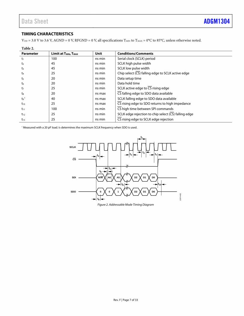
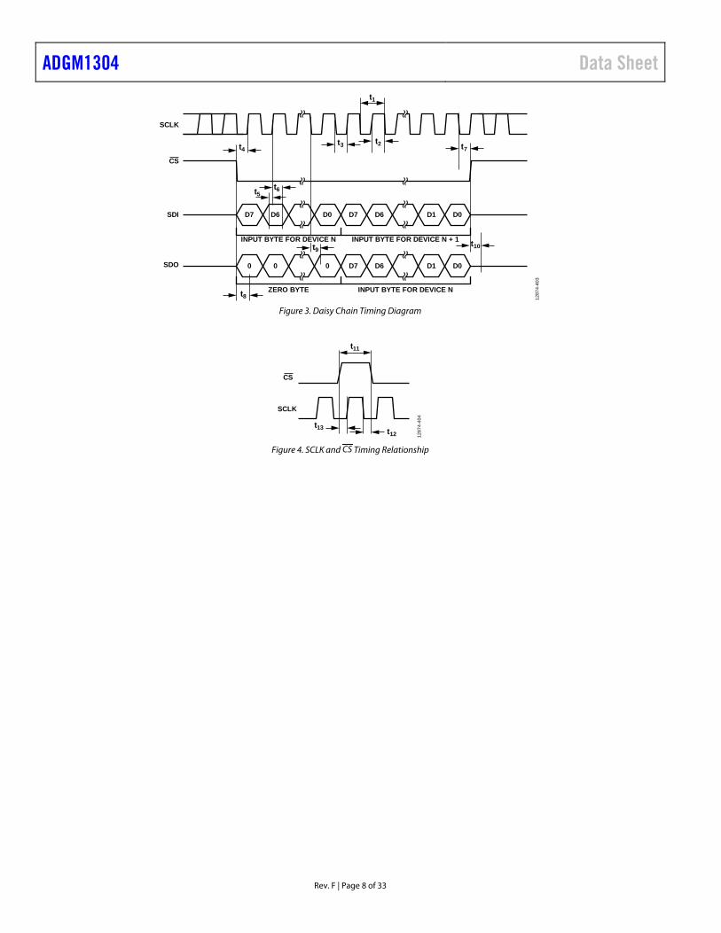
TIMING CHARACTERISTICS VDD = 3.0 V to 3.6 V, AGND = 0 V, RFGND = 0 V, all specifications TMIN to TMAX = 0°C to 85°C, unless otherwise noted.
Table 2. Parameter Limit at TMIN, TMAX Unit Conditions/Comments t1 100 ns min Serial clock (SCLK) period t2 45 ns min SCLK high pulse width t3 45 ns min SCLK low pulse width t4 25 ns min Chip select (CS) falling edge to SCLK active edge
t5 20 ns min Data setup time t6 20 ns min Data hold time t7 25 ns min SCLK active edge to CS rising edge
t8 20 ns max CS falling edge to SDO data available
t91 40 ns max SCLK falling edge to SDO data available
t10 25 ns max CS rising edge to SDO returns to high impedance
t11 100 ns min CS high time between SPI commands
t12 25 ns min SCLK edge rejection to chip select (CS) falling edge
t13 25 ns min CS rising edge to SCLK edge rejection 1 Measured with a 20 pF load. t9 determines the maximum SCLK frequency when SDO is used.
t1
t2t3t4
t5
t8
t9 t10
t6
t7
R/W
CS
SCLK
SDI
SDO
A6 A5 D2 D1 D0
0 0 1 D2 D1 D0
1287
4-40
2
Figure 2. Addressable Mode Timing Diagram
ADGM1304 Data Sheet
Rev. F | Page 8 of 33
t1
t2t3t4
t5
t8
t9t10
t6
t7
CS
SCLK
SDI
SDO
INPUT BYTE FOR DEVICE N + 1
ZERO BYTE INPUT BYTE FOR DEVICE N
D7 D6 D0 D7 D6 D1 D0
0 0 0 D7 D6 D1 D0
1287
4-40
3
INPUT BYTE FOR DEVICE N
Figure 3. Daisy Chain Timing Diagram
t13
t11
t12
CS
SCLK12
874-
404
Figure 4. SCLK and CS Timing Relationship
Data Sheet ADGM1304
Rev. F | Page 9 of 33
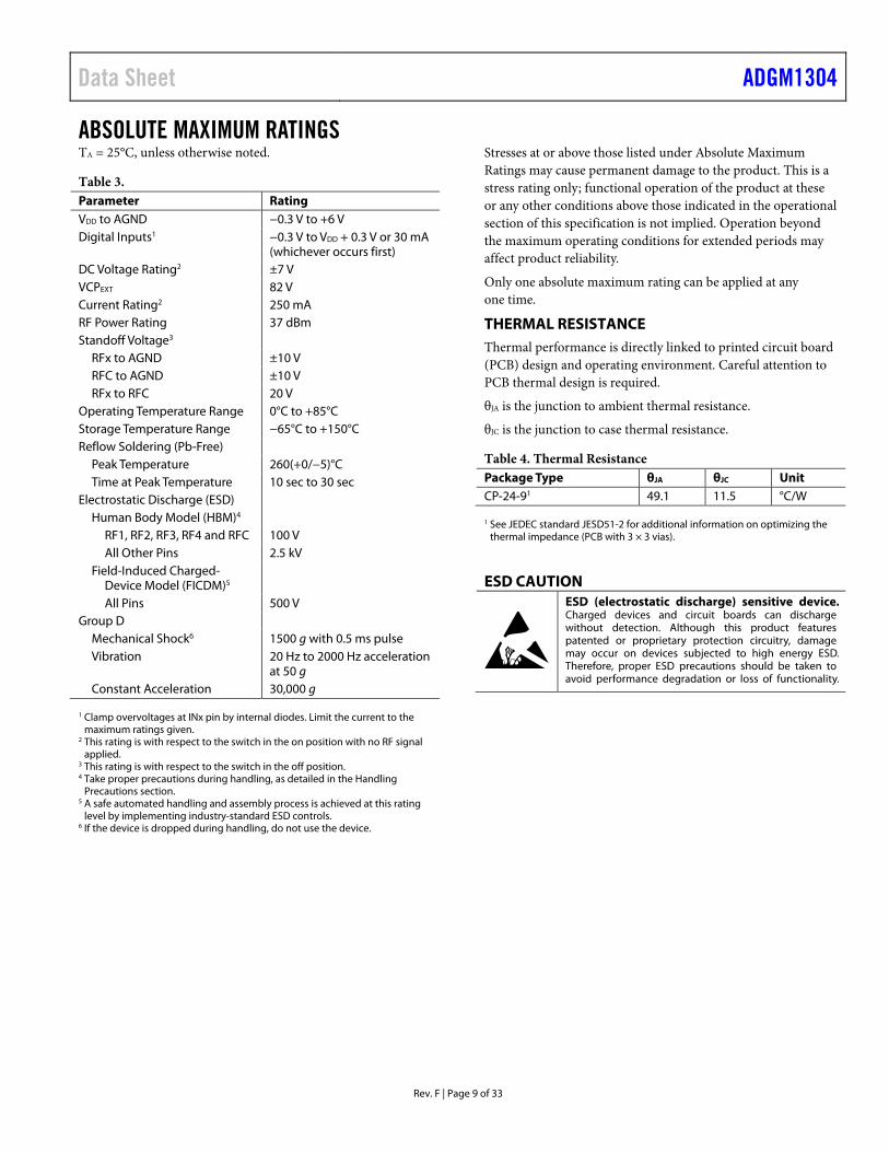
ABSOLUTE MAXIMUM RATINGS TA = 25°C, unless otherwise noted.
Table 3. Parameter Rating VDD to AGND −0.3 V to +6 V Digital Inputs1 −0.3 V to VDD + 0.3 V or 30 mA
(whichever occurs first) DC Voltage Rating2 ±7 V VCPEXT 82 V Current Rating2 250 mA RF Power Rating 37 dBm Standoff Voltage3
RFx to AGND ±10 V RFC to AGND ±10 V RFx to RFC 20 V
Operating Temperature Range 0°C to +85°C Storage Temperature Range −65°C to +150°C Reflow Soldering (Pb-Free)
Peak Temperature 260(+0/−5)°C Time at Peak Temperature 10 sec to 30 sec
Electrostatic Discharge (ESD) Human Body Model (HBM)4
RF1, RF2, RF3, RF4 and RFC 100 V All Other Pins 2.5 kV
Field-Induced Charged-Device Model (FICDM)5
All Pins 500 V Group D
Mechanical Shock6 1500 g with 0.5 ms pulse Vibration 20 Hz to 2000 Hz acceleration
at 50 g Constant Acceleration 30,000 g
1 Clamp overvoltages at INx pin by internal diodes. Limit the current to the
maximum ratings given. 2 This rating is with respect to the switch in the on position with no RF signal
applied. 3 This rating is with respect to the switch in the off position. 4 Take proper precautions during handling, as detailed in the Handling
Precautions section. 5 A safe automated handling and assembly process is achieved at this rating
level by implementing industry-standard ESD controls. 6 If the device is dropped during handling, do not use the device.
Stresses at or above those listed under Absolute Maximum Ratings may cause permanent damage to the product. This is a stress rating only; functional operation of the product at these or any other conditions above those indicated in the operational section of this specification is not implied. Operation beyond the maximum operating conditions for extended periods may affect product reliability.
Only one absolute maximum rating can be applied at any one time.
THERMAL RESISTANCE Thermal performance is directly linked to printed circuit board (PCB) design and operating environment. Careful attention to PCB thermal design is required.
θJA is the junction to ambient thermal resistance.
θJC is the junction to case thermal resistance.
Table 4. Thermal Resistance Package Type θJA θJC Unit CP-24-91 49.1 11.5 °C/W 1 See JEDEC standard JESD51-2 for additional information on optimizing the
thermal impedance (PCB with 3 × 3 vias).
ESD CAUTION

ADGM1304 Data Sheet
Rev. F | Page 10 of 33
PIN CONFIGURATION AND FUNCTION DESCRIPTIONS
NOTES1. EXPOSED PAD 1. EP1 IS INTERNALLY CONNECTED TO AGND. IT IS RECOMMENDED TO CONNECT TO BOTH AGND AND REFGND.2. EXPOSED PAD 2. EP2 IS INTERNALLY CONNECTED TO RFGND. IT IS RECOMMENDED TO CONNECT TO BOTH REFGND AND AGND. 12
874-
002
IN1/SDIIN2/CS
IN3/SCLKIN4/SDO
EP1 EP2AGND
REFGNDREFGNDRFCRFGNDRFGND
12345
1716151413
PIN
/SPI
EXTD
_EN
AG
ND
RFG
ND
RF4
6 7 8 9 10R
FGN
D11
RF3
VC
PV
DD
AG
ND
RFG
ND
RF1
RFG
ND
RF2
12
24 23 22 21 20 19 18
ADGM1304TOP VIEW
(Not to Scale)
Figure 5. Pin Configuration
Table 5. Pin Function Descriptions Pin No. Mnemonic Description 1 IN1/SDI Parallel Logic Digital Control Input 1. The voltage applied to this pin controls the gate of the RF1 to RFC
MEMS switch. In parallel mode, if the IN1 pin is low, the RF1 to RFC switch is open (off ). If the IN1 pin is high, the RF1 to RFC switch is closed (on). In SPI mode, this pin is the serial data input (SDI) pin.
2 IN2/CS Parallel Logic Digital Control Input 2. The voltage applied to this pin controls the gate of the RF2 to RFC MEMS switch. In parallel mode, if IN2 is low, the RF2 to RFC switch is open (off ). If IN2 is high, the RF2 to RFC switch is closed (on). In SPI mode, this pin is the chip select (CS ) pin. CS is an active low signal that selects the slave device with which the master device intends to communicate. Typically, there is a dedicated CS between the master device and each slave device. The CS pin also functions to synchronize and frame the communications to and from the slave device.
3 IN3/SCLK Parallel Logic Digital Control Input 3. The voltage applied to this pin controls the gate of the RF3 to RFC MEMS switch. In parallel mode, if IN3 is low, the RF3 to RFC switch is open (off ). If IN3 is high, the RF3 to RFC switch is closed (on). In SPI mode, this pin is the serial clock (SCLK) pin that synchronizes the slave device(s) to the master device. Typically, the SCLK signal is shared for all slave devices on the serial bus. The SCLK signal is always driven by the master device.
4 IN4/SDO Parallel Logic Digital Control Input 4. The voltage applied to this pin controls the gate of the RF4 to RFC MEMS switch. In parallel mode, if IN4 is low, the RF4 to RFC switch is open (off ). If IN4 is high, the RF4 to RFC switch is closed (on). In SPI mode, this pin is the serial data output (SDO) pin. Typically, the SDO pin is shared for all slave devices on the serial bus. The SDO pin is driven by only one slave device at a time, otherwise it is high impedance. The SDO pin is always high impedance when CS is deasserted high.
5, 8, 22 AGND Analog Ground Connection. 6 PIN/SPI Parallel Mode Enable/SPI Mode Enable. The SPI interface is enabled when this pin is high, and the parallel
interface (IN1, IN2, IN3, IN4) is enabled when this pin is low. 7 EXTD_EN External Voltage Drive Enable. In normal operation, set EXTD_EN low to enable the built in 10 MHz
oscillator, which enables the internal driver IC voltage boost circuitry. Setting EXTD_EN high disables the internal 10 MHz oscillator and driver boost circuitry. With the oscillator disabled, the switch can still be controlled via the logic interface pins (IN1 to IN4) or via the SPI interface, but the VCP pin must be driven with 80 V dc from an external voltage supply. In this mode, the ADGM1304 only consumes 50 µA maximum supply current. Disabling the internal oscillator eliminates the associated 10 MHz noise feedthrough from the switch.
9, 11, 13, 14, 16, 17, 19, 21
RFGND RF Ground Connection.
10 RF4 RF4 Port. This pin can be an input or an output. If unused, the pin must be connected to RFGND or terminate the pin with a 50 Ω resistor to RFGND.
12 RF3 RF3 Port. This pin can be an input or an output. If unused, the pin must be connected to RFGND or terminate the pin with a 50 Ω resistor to RFGND.
15 RFC Common RF Port. This pin can be an input or an output. 18 RF2 RF2 Port. This pin can be an input or an output. If unused, the pin must be connected to RFGND or terminate
the pin with a 50 Ω resistor to RFGND.
Data Sheet ADGM1304
Rev. F | Page 11 of 33
Pin No. Mnemonic Description 20 RF1 RF1 Port. This pin can be an input or an output. If unused, the pin must be connected to RFGND or terminate
the pin with a 50 Ω resistor to RFGND. 23 VDD Positive Power Supply Input. The recommended decoupling capacitor to ground value is 0.1 μF. For the
recommended input voltage for this chip, see the Specifications section. 24 VCP Charge Pump Capacitor Terminal. The recommended shunt capacitor to ground value is 47 pF (100 V rated).
If EXTD_EN is high, an 80 V dc drive voltage must be input into VCP to drive the switches. EP1 Exposed Pad 1. EP1 is internally connected to AGND. It is recommended to connect to both AGND and RFGND. EP2 Exposed Pad 2. EP2 is internally connected to RFGND. It is recommended to connect to both RFGND and AGND.
ADGM1304 Data Sheet
Rev. F | Page 12 of 33
TYPICAL PERFORMANCE CHARACTERISTICS
0
10
20
30
40
50
60
70
80
90
100
0 1 2 3 4 5 6
POPU
LATI
ON
(%)
ABSOLUTE RON (Ω)
1 ACTUATION167 MILLION ACTUATIONS500 MILLION ACTUATIONS1 BILLION ACTUATIONS
SWITCH ACTUATED AT 85°CRON MEASURED AT 25°CVDD = 3.3V
1287
4-50
6
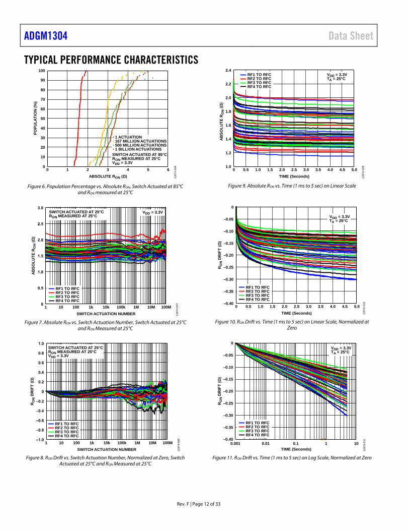
Figure 6. Population Percentage vs. Absolute RON, Switch Actuated at 85°C
and RON measured at 25°C
1 10 100 1k 10k 100k 1M 10M 100M
AB
SOLU
TE R
ON
(Ω)
SWITCH ACTUATION NUMBER
RF1 TO RFCRF2 TO RFCRF3 TO RFCRF4 TO RFC
SWITCH ACTUATED AT 25°CRON MEASURED AT 25°C
VDD = 3.3V
1287
4-50
7
Figure 7. Absolute RON vs. Switch Actuation Number, Switch Actuated at 25°C
and RON Measured at 25°C
1 10 100 1k 10k 100k 1M 10M 100M
RO
N D
RIF
T (Ω
)
SWITCH ACTUATION NUMBER
RF1 TO RFCRF2 TO RFCRF3 TO RFCRF4 TO RFC
1287
4-50
8
SWITCH ACTUATED AT 25°CRON MEASURED AT 25°CVDD = 3.3V
Figure 8. RON Drift vs. Switch Actuation Number, Normalized at Zero, Switch
Actuated at 25°C and RON Measured at 25°C
1.0
1.2
1.4
1.6
1.8
2.0
2.2
2.4
0 0.5 1.0 1.5 2.0 2.5 3.0 3.5 4.0 4.5 5.0
AB
SOLU
TE R
ON
(Ω)
TIME (Seconds)
VDD = 3.3VTA = 25°C
1287
4-50
9
RF1 TO RFCRF2 TO RFCRF3 TO RFCRF4 TO RFC
Figure 9. Absolute RON vs. Time (1 ms to 5 sec) on Linear Scale
1287
4-51
0–0.40
–0.35
–0.30
–0.25
–0.20
–0.15
–0.10
–0.05
0
0 0.5 1.0 1.5 2.0 2.5 3.0 3.5 4.0 4.5 5.0
RO
N D
RIF
T (Ω
)
TIME (Seconds)
VDD = 3.3VTA = 25°C
RF1 TO RFCRF2 TO RFCRF3 TO RFCRF4 TO RFC
Figure 10. RON Drift vs. Time (1 ms to 5 sec) on Linear Scale, Normalized at
Zero
1TIME (Seconds)
–0.40
–0.35
–0.30
–0.25
–0.20
–0.15
–0.10
–0.05
0
0.001 0.01 0.1 10
RO
N D
RIF
T (Ω
)
VDD = 3.3VTA = 25°C
1287
4-51
1
RF1 TO RFCRF2 TO RFCRF3 TO RFCRF4 TO RFC
Figure 11. RON Drift vs. Time (1 ms to 5 sec) on Log Scale, Normalized at Zero

Data Sheet ADGM1304
Rev. F | Page 13 of 33
0
0.2
0.4
0.6
0.8
1.0
1.2
1.4
1.6
1.8
2.0
–6 –4 –2 0 2 4 6
RO
N (Ω
)
SIGNAL BIAS VOLTAGE (V)
VDD = 3.0VVDD = 3.3VVDD = 3.6V
TA = 25°C
1287
4-52
2
Figure 12. RON vs. Signal Bias Voltage over Supply Voltages (Measured 5 sec Post Switch Turn On Time, RF1 to RFC On)
–6 –4 –2 0 2 4 6
RO
N (Ω
)
SIGNAL BIAS VOLTAGE (V)
VDD = 3.3VTA = 0°CTA = 25°CTA = 85°C
1287
4-51
3
Figure 13. RON vs. Signal Bias Voltage over Temperature (Measured 5 sec Post Switch Turn On Time, RF1 to RFC On)
10k 100k 1M 10M
SWITCH ACTUATIONS (Cycles)
FAIL
UR
ES (%
OF
POPU
LATI
ON
)
100M 1B 10B 100B
98
949082
65T50
45
25
148
4
1
1287
4-42
1
15dBm10dBm
20dBm
Figure 14. Hot Switching Probability Distribution on Log Normal with 95% Confidence Interval (CI), RF Power = Continuous Wave, Terminated into 50
Ω, TA = 25°C, VDD = 3.3 V
–3.0
–2.5
–2.0
–1.5
–1.0
–0.5
0
0 2 4 6 8 10 12 14 16
INSE
RTI
ON
LO
SS (d
B)
FREQUENCY (GHz)
25°C RF125°C RF2
1287
4-10
3
Figure 15. Insertion Loss vs. Frequency on Linear Scale (VDD = 3.3 V)
0 2 4 6 8 10 12 14 16–3.0
–2.5
–2.0
–1.5
–1.0
–0.5
0
INSE
RTI
ON
LO
SS (d
B)
FREQUENCY (GHz)
+85°C RF1+25°C RF10°C RF1
1287
4-10
5
Figure 16. Insertion Loss vs. Frequency over Temperature on Linear Scale (VDD = 3.3 V, RF1 to RFC)
–80
–70
–60
–50
–40
–30
–20
–10
0
–0.50
–0.45
–0.40
–0.35
–0.30
–0.25
–0.20
–0.15
–0.10
–0.05
0
0 50M 100M 150M 200M
OFF
ISO
LATI
ON
/RET
UR
N L
OSS
(dB
)
INSE
RTI
ON
LO
SS (d
B)
FREQUENCY (Hz)
TA = 25°CVDD = 3.3V
INSERTION LOSSOFF ISOLATIONRETURN LOSS
1287
4-00
4
Figure 17. Insertion Loss and Off Isolation/Return Loss vs.
Frequency (VDD = 3.3 V, RF1 to RFC)

ADGM1304 Data Sheet
Rev. F | Page 14 of 33
–80
–70
–60
–50
–40
–30
–20
–10
0
0 2 4 6 8 10
OFF
ISO
LATI
ON
(dB
)
FREQUENCY (GHz)
TA = 25°CVDD = 3.3V
RF1 TO RFCRF2 TO RFC
1287
4-00
6
Figure 18. Off Isolation vs. Frequency, All Switches Off (VDD = 3.3 V)
–80
–70
–60
–50
–40
–30
–20
–10
0
0 1 2 3 4 5 6 7 8 9 10
OFF
ISO
LATI
ON
(dB
)
FREQUENCY (GHz)
RF2 TO RFCRF3 TO RFCRF4 TO RFC
TA = 25°CVDD = 3.3V
1287
4-41
2
Figure 19. Off Isolation vs. Frequency, RF1 to RFC On (VDD = 3.3 V)
–80
–70
–60
–50
–40
–30
–20
–10
0
CR
OSS
TALK
(dB
)
0 1 2 3 4 6 7 8 95 10FREQUENCY (GHz)
1287
4-00
7
TA = 25°CVDD = 3.3V
RF1 TO RF2RF2 TO RF1
Figure 20. Crosstalk vs. Frequency (VDD = 3.3 V)
–60
–50
–40
–30
–20
–10
0
0 1 2 3 4 6 7 8 95 10
RET
UR
N L
OSS
(dB
)
FREQUENCY (GHz)
TA = 25°CVDD = 3.3V
RF1RF2
1287
4-00
8
Figure 21. Return Loss vs. Frequency (VDD = 3.3 V)
0
1 10 100 1k 10k 100k 1M 10M 100M
INSE
RTI
ON
LO
SS (d
B)
SWITCH TOGGLES
–0.50
–0.45
–0.40
–0.35
–0.30
–0.25
–0.20
–0.15
–0.10
–0.05
2.5GHz RF1 TO RFC6.0GHz RF1 TO RFC
1287
4-01
0
TA = 25°CVDD = 3.3V
Figure 22. Insertion Loss vs. Switch Toggles (VDD = 3.3 V)
0
20
40
–0.7
00–0
.675
–0.6
50–0
.625
–0.6
00–0
.575
–0.5
50–0
.525
–0.5
00–0
.475
–0.4
50–0
.425
–0.4
00–0
.375
–0.3
50–0
.325
–0.3
00–0
.275
–0.2
50–0
.225
–0.2
00–0
.175
–0.1
50–0
.125
–0.1
00–0
.075
–0.0
50–0
.025 0
60
100
80
120
SAM
PLE
NU
MB
ER
INSERTION LOSS (dB) 1287
4-01
4
HISTOGRAM DATA ISCOLLECTED USING A SOCKETEDTEST BOARD AND INCLUDESASSOCIATED LOSSES
2.5GHz AT 25°C2.5GHz AT 85°C
2.5GHz AT 0°C
VDD = 3.3V
Figure 23. 2.5 GHz Insertion Loss Histogram at Various Temperatures, VDD = 3.3 V

Data Sheet ADGM1304
Rev. F | Page 15 of 33
HISTOGRAM DATA ISCOLLECTED USING A SOCKETEDTEST BOARD AND INCLUDESASSOCIATED LOSSES
SAM
PLE
NU
MB
ER
INSERTION LOSS (dB)
6.0GHz AT 25°C6.0GHz AT 85°C
6.0GHz AT 0°C
1287
4-01
5
VDD = 3.3V
Figure 24. 6.0 GHz Insertion Loss Histogram at Various Temperatures, (VDD = 3.3 V
–1.0
–0.8
–0.6
–0.4
–0.2
0
0.2
0.4
0.6
0.8
1.0
–0.5
0
0.5
1.0
1.5
2.0
2.5
3.0
3.5
0 10 20 30 40
TEST
SIG
NAL
(V)
DIG
ITA
L C
ON
TRO
L SI
GN
AL (V
)
TIME (µs)
TA = 25°CVDD = 3.3V
DIGITAL CONTROLtON/tOFF TEST SIGNAL
1287
4-01
2
Figure 25. Digital Control Signal and Test Signal vs. Time (VDD = 3.3 V)
–120
–100
–80
–60
–40
–20
0
0 2 4 6 8 10 12
THD
+ N
(dB
c)
SIGNAL AMPLITUDE (V p-p)
100Hz1kHz5kHz10kHz15kHz20kHz
1287
4-42
5
Figure 26. THD + N vs. Signal Amplitude, VDD = 3.3 V, RLOAD = 300 Ω, TA = 25°C, Signal Source Impedance = 20 Ω
–120
–110
–100
–90
–80
–70
–60
–50
–40
–30
–20
–10
0
THD
+ N
(dB
c)
FREQUENCY (kHz)0 2 4 6 8 10 12 14 16 18 20
1287
4-42
6
0dBm5dBm10dBm14.5dBm
Figure 27. THD + N vs. Frequency, VDD = 3.3 V, RLOAD = 300 Ω, TA = 25°C, Signal Source Impedance = 20 Ω
0
0.5
1.0
1.5
2.0
2.5
3.0
3.5
4.0
–6 –4 –2 0 2 4 6
SWIT
CH
CA
PAC
ITA
NC
E (p
F)
SIGNAL BIAS VOLTAGE (V)
OFF SWITCH CAPACITANCEON SWITCH CAPACITANCE
1287
4-52
8
Figure 28. Switch Capacitance vs. Signal Bias Voltage
0
4
8
12
16
20
24
28
32
36
0 4 8 12 16 20 24 28 32 36
OU
TPU
TPO
WER
(dB
m)
INPUT POWER (dBm) 1287
4-43
5
Figure 29. Output Power vs. Input Power (Signal Frequency = 4 GHz, VDD = 3.3 V, TA = 25°C)

ADGM1304 Data Sheet
Rev. F | Page 16 of 33
–5.0
–4.5
–4.0
–3.5
–3.0
–2.5
–2.0
–1.5
–1.0
–0.5
0
0 4 8 12 16 20 24 28 32 36
INSE
RTI
ON
LO
SS (d
B)
INPUT POWER (dBm)
VDD = 3.3VTA = 25°CFREQUENCY = 4GHz
1287
4-53
0
Figure 30. Insertion Loss vs. Input Power
–136
–134
–132
–130
–128
–126
–124
–122
–120
10.17 10.19 10.21 10.23 10.25 10.27
OSC
ILLA
TOR
FEED
THR
OU
GH
(dB
)
FREQUENCY (MHz) 1287
4-43
7
TA = 25°CVDD = 3.3V
Figure 31. Oscillator Feedthrough, Zoomed In at 10.2 MHz
–136
–134
–132
–130
–128
–126
–124
–122
–120
0 10 20 30 40 50 60 70 80 90 100
OSC
ILLA
TOR
FEE
DTH
RO
UG
H (d
B)
FREQUENCY (MHz)
NORMAL OPERATING MODEINTERNAL OSCILLATOR DISABLED
1287
4-43
8
TA = 25°CVDD = 3.3V
Figure 32. Oscillator Feedthrough Wide Bandwidth
Data Sheet ADGM1304
Rev. F | Page 17 of 33
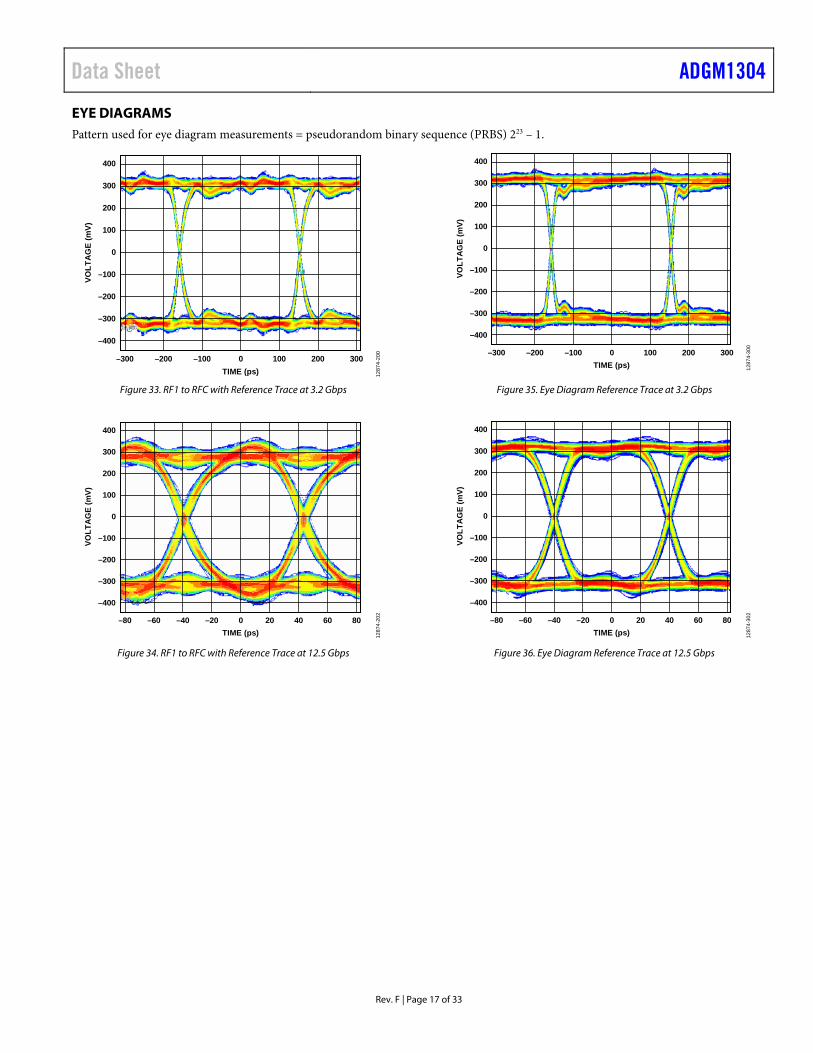
EYE DIAGRAMS Pattern used for eye diagram measurements = pseudorandom binary sequence (PRBS) 223 – 1.
–400
–300
–200
–100
0
100
200
300
400
–300 –200 –100 0 100 200 300
VOLT
AG
E (m
V)
TIME (ps) 1287
4-20
0
Figure 33. RF1 to RFC with Reference Trace at 3.2 Gbps
–400
–300
–200
–100
0
100
200
300
400
–80 –60 –40 –20 0 20 40 60 80
VOLT
AG
E (m
V)
TIME (ps) 1287
4-20
2
Figure 34. RF1 to RFC with Reference Trace at 12.5 Gbps
–400
–300
–200
–100
0
100
200
300
400
–300 –200 –100 0 100 200 300
VOLT
AG
E (m
V)
TIME (ps) 1287
4-30
0
Figure 35. Eye Diagram Reference Trace at 3.2 Gbps
–400
–300
–200
–100
0
100
200
300
400
–80 –60 –40 –20 0 20 40 60 80
VOLT
AG
E (m
V)
TIME (ps) 1287
4-30
2
Figure 36. Eye Diagram Reference Trace at 12.5 Gbps
ADGM1304 Data Sheet
Rev. F | Page 18 of 33
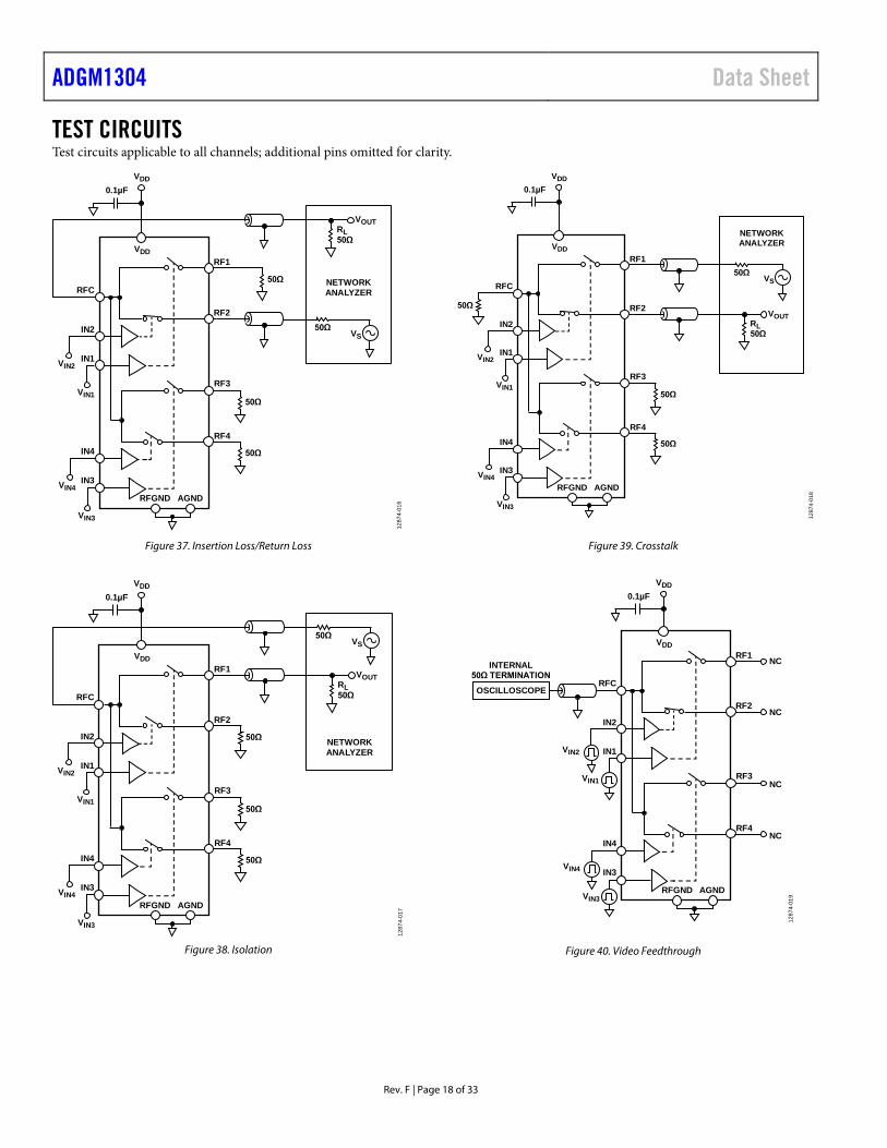
TEST CIRCUITS Test circuits applicable to all channels; additional pins omitted for clarity.
VS50Ω
VOUTRL50Ω
VIN2
VDD
0.1µFVDD
RF2
RF1
IN2
RFC
VIN1RF3
50Ω
IN1
50Ω
50Ω
RF4
VIN4
IN4
VIN3
IN3
AGNDRFGND
1287
4-01
6
NETWORKANALYZER
Figure 37. Insertion Loss/Return Loss
VS
NETWORKANALYZER
50Ω
VOUTRL50Ω
VIN2
VDD
0.1µFVDD
RF2
RF1
IN2
RFC
VIN1RF3
50Ω
IN1
50Ω
RF4
VIN4
IN4
VIN3
IN3
50Ω
1287
4-01
7AGNDRFGND
Figure 38. Isolation
VIN2
VDD
0.1µFVDD
RF2
RF1
IN2
RFC
VIN1RF3
50Ω
IN1
50Ω
50Ω
RF4
VIN4
IN4
VIN3
IN3
1287
4-01
8
VS
NETWORKANALYZER
50Ω
VOUTRL50Ω
AGNDRFGND
Figure 39. Crosstalk
VIN2
VDD
0.1µFVDD
RF2
RF1
IN2
NC
NC
NC
NC
RFCOSCILLOSCOPE
INTERNAL50Ω TERMINATION
VIN1 RF3
IN1
RF4
VIN4
IN4
VIN3
IN3
1287
4-01
9
AGNDRFGND
Figure 40. Video Feedthrough

Data Sheet ADGM1304
Rev. F | Page 19 of 33
0.1µF
VIN2
VDD
VDD
RF1
RF2
IN2
RFC
VIN1RF3
50Ω
IN1
50Ω
50Ω
RF4
VIN4
IN4
VIN3
IN312
874-
020
SPECTRUMANALYZER
COMBINERNETWORK
RFSOURCE
RFSOURCE
AGNDRFGND
Figure 41. Input Second-Order Intermodulation Intercept (IIP2) and Input Third-Order Intermodulation Intercept (IIP3)
tON
50% 50%
90% 10%
VINx
VOUT
tOFF
VDD
VDD
0.1µF
VS
VINx
INx
RFxRFC
RL50Ω
VOUT
1287
4-02
1
AGNDRFGND
Figure 42. Switch Timings, tON and tOFF
0.1µF
VIN2
VDDRF1
RF2
IN2
RFC
VIN1RF3
50Ω
IN1
50Ω
50Ω
RF4
VIN4
IN4
VIN3
IN3
50Ω
1287
4-52
1
RFSOURCE
INPUT
RFAMPLIFIER
VDD
GNDGND
Figure 43. Hot Switching Evaluation Setup, 2 GHz RF Source, 50% Duty Cycle, 5 kHz Switching Frequency
1287
4-20
3
VDD
VDD
0.1µF
VINx
INx
RFxRFC
AGNDRFGND
V
Figure 44. On Resistance

ADGM1304 Data Sheet
Rev. F | Page 20 of 33
0.1µF
VIN2
VDDRF1
RF2
IN2
RFC
VIN1RF3
50Ω
IN1
50Ω
50Ω
RF4
VIN4
IN4
VIN3
IN3
1287
4-02
3
SPECTRUMANALYZER
RFSOURCE
INPUTRF
AMPLIFIER
VDD
AGNDRFGND
Figure 45. Second and Third Harmonics, RF Power
VIN2
VDD
0.1µFVDD
RF2
RF1
IN2
RFC
VIN1 RF3
IN1
RF4
VIN4
IN4
VIN3
IN3
-6VNCA
-6V
-6V
-6V
NC = NO CONNECT 1287
4-45
4
AGNDRFGND
Figure 46. On Leakage
VIN2
VDD
0.1µFVDD
RF2
RF1
IN2
RFC
VIN1RF3
IN1
RF4
VIN4
IN4
VIN3
IN3
GNDGND
-6VA
6V
6V
6V
NC = NO CONNECT
A
6V
A
A
A
1287
4-45
1
Figure 47. Off Leakage

Data Sheet ADGM1304
Rev. F | Page 21 of 33
TERMINOLOGY Insertion Loss (IL) IL is the amount of signal attenuation between the input and output ports of the switch when the switch is in the on state. IL is expressed in decibels. Ensure that insertion loss is as small as possible for maximum power transfer.
An example calculation of insertion loss based on the setup in Figure 37 is as follows:
IL = −20log10|SRF2RFC|
where SRF2RFC is the transmission coefficient measured from RF2 to RFC with RF2 in the on position.
All unused switches are in the off position and terminated in a purely resistive load of 50 Ω.
Isolation (ISO) ISO is the amount of signal attenuation between the input and output ports of the switch when the switch is in the off state. ISO is expressed in decibels. Ensure that isolation is as large as possible.
An example calculation of isolation based on the setup in Figure 38 is as follows:
ISO = −20log10|SRFCRF1|
where SRFCRF1 is the transmission coefficient measured from RFC to RF1 with RF1 in the off position.
All unused switches are in the off position and terminated in a purely resistive load of 50 Ω.
Crosstalk (CTK) CTK is a measure of unwanted signals coupled through from one channel to another because of parasitic capacitance. CTK is expressed in decibels.
An example calculation of crosstalk based on the setup in Figure 39 is as follows:
CTK = −20log10|SRF1RF2|
where SRF1RF2 is the transmission coefficient measured from RF1 to RF2 with RF1 in the off position and RF2 in the on position.
All unused switches are in the off position and terminated in a purely resistive load of 50 Ω.
Return Loss (RL) RL is the magnitude of the reflection coefficient (expressed in decibels), and the amount of reflected signal relative to the incident signal.
An example calculation of return loss based on the setup in Figure 37 is as follows:
RL = −20log10|S11|
where S11 is the reflection coefficient of the port under test.
Third-Order Intermodulation Intercept (IIP3) IP3 is the intersection point of the fundamental output power (POUT) vs. input power (PIN) extrapolated line and the third-order intermodulation products extrapolated line of a two tone test. IIP3 is a figure of merit that characterizes the switch linearity.
Second-Order Intermodulation Intercept (IIP2) IIP2 is the intersection point of the fundamental POUT vs. PIN extrapolated line and the second-order intermodulation products extrapolated line of a two tone test. IIP2 is a figure of merit that characterizes the switch linearity.
Second Harmonic (HD2) HD2 is the amplitude of the second harmonic, where, for a signal whose fundamental frequency is f, the second harmonic has a frequency 2f. This measurement is a single tone test, expressed with reference to the carrier signal (dBc).
Third Harmonic (HD3) HD3 is the amplitude of the third harmonic, where, for a signal whose fundamental frequency is f, the third harmonic has a frequency 3f. This measurement is a single tone test, expressed with reference to the carrier signal (dBc).
RF Power Rating The RF power rating is the maximum level of RF power that passes through the switch without degradation to the switch lifetime when it is in the on state.
On Switching Time (tON) tON is the time it takes for the switch to turn on. It is measured from 50% of the control signal (INx) to 90% of the on level. No power is applied through the switch during this test (cold switched). The switch is terminated into a 50 Ω load.
Off Switching Time (tOFF) tOFF is the time it takes for the switch to turn off. It is measured from 50% of the control signal (INx) to 10% of the on level. No power is applied through the switch during this test (cold switched). The switch is terminated into a 50 Ω load.
Actuation Frequency The actuation frequency refers to the speed at which the ADGM1304 can be switched on and off. It is dependent on both settling times and on to off switching times.
Wake-Up Time The wake-up time is a measure of the time required for the voltage on VCP to reach the typical voltage of 80 V after the device exits sleep mode.
Video Feedthrough Video feedthrough is a measure of the spurious signals present at the RF ports of the switch when the control voltage is switched from high to low or from low to high without an RF signal present.
ADGM1304 Data Sheet
Rev. F | Page 22 of 33
Internal Oscillator Frequency The internal oscillator frequency is the value of the on-board oscillator that drives the gate control chip of the ADGM1304.
Internal Oscillator Feedthrough The internal oscillator feedthrough is the amount of internal oscillator signal that feeds through to the RF pins of the switch. This signal appears as a noise spur on the RFx pin and RFC pin of the switch at the oscillator operating frequency and oscillator harmonics.
On Resistance (RON) RON is the resistance of a switch in the closed (on) state measured between the package pins. Measure on resistance in 4-wire mode to eliminate any cabling or PCB series resistances.
On Resistance Drift On resistance drift is the change in the on resistance of the switch over the specified criteria in Table 1.
Continuously on Lifetime The continuously on lifetime measures how long the switch is left in a continuously on state. If the switch is left in the on position for an extended period, it affects the turn off mechanism of the device.
Actuation Lifetime Actuation lifetime is the number of consecutive open to close to open cycles that can complete without the on resistance exceeding a specified limit and no occurrence of failures to open (FTO) or failures to close (FTC).
Cold Switching Cold switching operates the switch in a mode so that no voltage differential exists between source and drain when the switch is
closed or no current is flowing from source to drain when the switch opens. All switches have longer lives when cold switched.
Hot Switching Hot switching is operating the switch in a mode where a voltage differential exists between source and drain when the switch is closed and/or current is flowing from RFx channel to RFC channel when the switch is opened. Hot switching results in a reduced switch life, depending on the magnitude of the open circuit voltage between the source and the drain.
Input High Voltage (VINH) VINH is the minimum input voltage for Logic 1.
Input Low Voltage (VINL) VINL is the maximum input voltage for Logic 0.
Input Current (IINL, IINH) IINL and IINH are the low and high input currents of the digital inputs.
Output High Voltage (VOH) VOH is the minimum output voltage for Logic 1.
Output Low Voltage (VOL) VOL is the maximum output voltage for Logic 0.
Low Power Mode Current (IDD EXT VCP) IDD EXT VCP is the amount of supply current used by the gate driver circuity when the internal oscillator and the charge pump circuitry are turned off by setting the EXTD_EN pin high.
External Drive Current (ICP EXT VCP) ICP EXT VCP is the amount of current used by the ADGM1304 from the external 80 V power supply when the internal oscillator and charge pump circuitry are turned off by setting the EXTD_EN pin high.

Data Sheet ADGM1304
Rev. F | Page 23 of 33
THEORY OF OPERATION The ADGM1304 is an SP4T switch fabricated using Analog Devices MEMS switch technology. This technology enables high power, low loss, low distortion GHz switches for use in demanding RF applications.
Figure 48 shows a stylized cross section graphic of the switch with dimensions. The switch is an electrostatically actuated cantilever beam connected in a three terminal configuration. Functionally, the switch is analogous to a field effect transistor (FET), and the terminals can be used as a source, gate, and drain.
1287
4-12
6
SILICON
SILICON
SOURCE DRAINCANTILEVER BEAM
GATE CONTACT GAP
METAL
Figure 48. Cross Section of the MEMS Switch Design Showing the Cantilever
Switch Beam (Not to Scale)
When a dc actuation voltage is applied between the gate electrode and the source (the switch beam), an electrostatic force is generated, which attracts the beam toward the substrate. A separate on-board charge pump IC generates the bias voltage, and 80 V is used for actuation.
When the bias voltage between the gate and the source exceeds the threshold voltage of the switch, VTH, the contacts on the beam touch the drain, which completes the circuit between the source and the drain and turns the switch on. When the bias voltage is removed (0 V on the gate electrode), the beam acts as a spring to generate a sufficient restoring force to open the connection between the source and the drain, break the circuit, and turn the switch off.
Figure 49 shows the SP4T MEMS switch and controller die within the LFCSP. Some of the LFCSP plastic molding material is removed to allow the MEMS switch die (right) and controller die (left) with associated wire bonds to be visible. The silicon hermetically sealed cap covering the switch die is the black
rectangle on the right. Hermetically sealing the switches improves the reliability and lifetime of the switches by keeping them in a controlled atmosphere. The switch contacts do not suffer from dry switching or low power switching lifetime degradation.
1287
4-12
7
Figure 49. ADGM1304 LFCSP Package with Molding Compound Partially
Removed to Show MEMS Switch Die (Right), Controller Die (Left), and Associated Wire Bonds
PARALLEL DIGITAL INTERFACE The ADGM1304 is controlled via a parallel interface. Standard CMOS/LVTTL signals applied through this interface control the actuation and release of all of the switch channels of the ADGM1304. Applied gate signals are boosted to give the required voltages needed to actuate the MEMS switches.
Setting the PIN/SPI pin low enables the parallel digital interface in 4-wire SP4T mode. In parallel mode, Pin 1 to Pin 4 (IN1 to IN4) control the switching functions of the ADGM1304. When a Logic 1 is applied to one of these pins, the gate of the corresponding switch is activated and the switch turns on. Conversely, when a Logic 0 is applied to one of these pins, the switch turns off. Note that it is possible to connect more than one RFx input to RFC at a time. Table 6 is the truth table for the ADGM1304.

ADGM1304 Data Sheet
Rev. F | Page 24 of 33
Table 6. Truth Table When in Parallel Digital Interface Mode IN1 IN2 IN3 IN4 RF1 to RFC RF2 to RFC RF3 to RFC RF4 to RFC 0 0 0 0 Off Off Off Off 0 0 0 1 Off Off Off On 0 0 1 0 Off Off On Off 0 0 1 1 Off Off On On 0 1 0 0 Off On Off Off 0 1 0 1 Off On Off On 0 1 1 0 Off On On Off 0 1 1 1 Off On On On 1 0 0 0 On Off Off Off 1 0 0 1 On Off Off On 1 0 1 0 On Off On Off 1 0 1 1 On Off On On 1 1 0 0 On On Off Off 1 1 0 1 On On Off On 1 1 1 0 On On On Off 1 1 1 1 On On On On X1 X1 X1 X1 Off Off Off Off 1 X means any logic state.
SPI DIGITAL INTERFACE The ADGM1304 can be controlled via an SPI digital interface when Pin 6 (PIN/SPI) is high. The SPI is compatible with SPI Mode 0 (clock polarity (CPOL) = 0, clock phase (CPHA) = 0) and Mode 3 (CPOL = 1, CPHA = 1) and it operates with SCLK frequencies up to 10 MHz. When the SPI is active, the default mode is addressable, in which, the device registers are accessed by a 16-bit SPI command that is bound by the state of the CS pin. The ADGM1304 can also operate in daisy-chain mode.
The SPI interface pins of the ADGM1304 are CS, SCLK, SDI, and SDO. Hold CS low when using the SPI interface. The data on SDI is captured on the rising edge of SCLK and data is propagated out on SDO on the falling edge of SCLK. SDO has push-pull output driver architecture that does not require pull-up resistors.
Addressable Mode
Addressable mode is the default mode for the ADGM1304 on power up. A single SPI frame in addressable mode is bounded by a CS falling edge and the succeedingCS rising edge. It is comprised of 16 SCLK cycles. The timing diagram for addressable mode is shown in Figure 50.
The first SDI bit indicates if the SPI command is a read or write command. The next seven bits determine the target register address. The remaining eight bits provide the data to the addressed register. The first eight bits are ignored during a read command, during which time the SDO propagates out the data contained in the addressed register.
The target register address of an SPI command is determined on the eighth SCLK rising edge. Data from the target register propagates out on the SDO from the ninth to the 16th SCLK falling edge during SPI reads. A register write occurs on the 16th SCLK rising edge during SPI writes. During any SPI command, SDO
sends out eight alignment bits on the first eight SCLK falling edges. The alignment bits observed at SDO are 0x25.
Daisy-Chain Mode
The connection of several ADGM1304 devices in a daisy-chain configuration is possible. All devices share the same CS and SCLK lines while the SDO pin of one device forms a connection to the SDI pin of the next device, creating a shift register. In daisy-chain mode, the SDO signal is an 8-cycle delayed version of the SDI signal (see Figure 52).
The ADGM1304 can only enter daisy-chain mode from address-able mode by sending the 16-bit SPI command, 0x2500. See Figure 52 for an example of this command. When the ADGM1304 receives this command, the SDO pin of the devices sends out the same command because the alignment bits at the SDO pin are 0x25. This command allows multiple daisy-chained devices to enter daisy-chain mode in a single SPI frame. A hardware reset is required to exit daisy-chain mode.
For the timing diagram of a typical daisy-chain SPI frame, see Figure 53. When the CS pin goes high, Device 1 writes Command 0 to Bits[7:0] to the SWITCH_DATA register, Device 2 writes Command 1 to Bits[7:0] to the switches, and so on. The SPI block uses the last eight bits received through the SDI pin to update the switches. After entering daisy-chain mode, the first eight bits sent out by the SDO pin are 0x00. When CS goes high, the internal shift register value does not reset back to 0.
An SCLK rising edge reads in data on the SDI pin while data is propagated out of the SDO pin on an SCLK falling edge. The expected number of SCLK cycles are a multiple of eight before the CS pin goes high. When this is not the case, the SPI interface sends the last eight bits received to the SWITCH_DATA register.

Data Sheet ADGM1304
Rev. F | Page 25 of 33
0 0 1 0 0 1 0 1 D7 D6 D5 D4 D3 D2 D1 D0SDO
R/W A6 A5 A4 A3 A2 A1 A0 D7 D6 D5 D4 D3 D2 D1 D0
1 2 3 4 5 6 7 8 9 10 11 12 13 14 15 16
SDI
SCLK
CS
1287
4-45
8
Figure 50. Addressable Mode Timing Diagram
RF4
SDICS
RF3
RF2
SDO
ADGM1304DEVICE 1
SPIINTERFACE
RFC
SCLK
RF4
RF3
RF2
SDO
ADGM1304DEVICE 2
SPIINTERFACE
RFC
1287
4-45
9
Figure 51. Two SPI-Controlled ADGM1304 Switches Connected in a Daisy-Chain Configuration
0 0 1 0 0 1 0 1 0 0 0 0 0 0 0 0SDO
0 0 1 0 0 1 0 1 0 0 0 0 0 0 0 0
1 2 3 4 5 6 7 8 9 10 11 12 13 14 15 16
SDI
SCLK
CS
1287
4-46
0
Figure 52. SPI Command to Enter Daisy-Chain Mode
SDO
COMMAND3[7:0]
8’h00
COMMAND2[7:0]
COMMAND3[7:0]
COMMAND1[7:0]
COMMAND2[7:0]
COMMAND0[7:0]
COMMAND1[7:0]
SDI
SDO3
8’h00
8’h00
8’h00
8’h00
COMMAND3[7:0]
8’h00
COMMAND2[7:0]
COMMAND3[7:0]
SDO2
DEVICE 2
DEVICE 1
DEVICE 4
DEVICE 3
CS
1287
4-46
1
NOTES1. SDO2 AND SDO3 ARE THE OUTPUT COMMANDS FROM DEVICE 2 AND DEVICE 3, RESPECTIVELY.
Figure 53. Example of a SPI Frame when Three ADGM1304 Devices are Connected in Daisy-Chain Mode
Hardware Reset
The digital portion of the ADGM1304 goes through an initialization phase during VDD power up. To hardware reset the ADGM1304, power cycle the VDD input. After power-up or a hardware reset, ensure there is a minimum of 10 µs before any SPI command is issued. Ensure that VDD does not drop out during the 10 µs initialization phase because it may result in incorrect operation of the ADGM1304.
Internal Error Status
When an internal error is detected in the device, the internal error is flagged by the INTERNAL_ERROR bits (Bits[7:6]) of the SWITCH_DATA register (Register 0x20), as shown in Table 10. An internal error results from an error in the configuration of the device at power up.

ADGM1304 Data Sheet
Rev. F | Page 26 of 33
INTERNAL OSCILLATOR FEEDTHROUGH The ADGM1304 has an internal oscillator running at a nominal 10 MHz. This oscillator drives the charge pump circuitry that provides the actuation voltage for each of the switch gate elec-trodes. Although this oscillator is very low power, the 10 MHz signal is coupled to the switch and can be considered a noise spur on the switch channels. The magnitude of this feedthrough noise spur is specified in Table 1 and is typically −123 dBm or −146 dBm/Hz when one switch is on. When all four switches are simultaneously on, the feedthrough goes up to −120 dBm. VDD level and temperature changes affect the frequency of the noise spur. For the maximum and minimum frequency range over temperature and voltage supply range, see Table 1.
INTERNAL OSCILLATOR FEEDTHROUGH MITIGATION In normal operation, the 80 V actuation voltage is supplied by the driver IC. Setting the EXTD_EN pin (Pin 7) low enables the built in 10 MHz oscillator. This setting enables the charge pump circuitry to generate the 80 V required for MEMS switch actuation. The internal oscillator is a source of noise which couples through to the RF ports. The magnitude of this feedthrough noise spur is specified in Table 1 and is typically −123 dBm or −146 dBm/Hz when one switch is on. The internal oscillator feedthrough can be eliminated by setting the EXTD_EN pin high, which disables the internal oscillator and charge pump circuitry. When the internal oscillator and charge pump circuitry is disabled, the VCP pin (Pin 24) must be driven with 80 V dc (VCPEXT) from an external voltage supply, as outlined in Table 5, required for MEMS switch actuation. The switch can still be controlled via the digital logic interface pins or via SPI interface pins
LOW POWER MODE Setting the EXTD_EN pin high shuts down the internal oscillator. The ADGM1304 enters low power quiescent state, drawing only 50 µA maximum supply current. When the internal oscillator and charge pump circuitry is disabled, the VCP pin (Pin 24) must be driven with 80 V dc (VCPEXT) from an external voltage supply, as outlined in Table 5, required for MEMS switch actuation. The switch can still be controlled via the digital logic interface pins or via SPI interface.
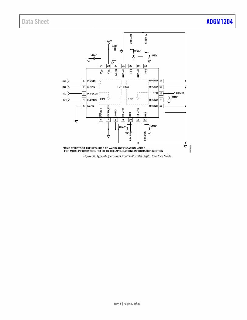
TYPICAL OPERATING CIRCUIT Figure 54 shows the typical operating circuit for the ADGM1304 as used in the EVAL-ADGM1304SDZ. A 47 pF (100 V rated) external capacitor is required on the VCP pin as a holding capacitor for the 80 V gate drive voltage. The VDD pin is connected to a 3.3 V supply. However, VDD can operate from 3.0 V to 3.6 V. RFGND is separated from AGND internally in the device.
It is recommended to connect RFGND to AGND using one large pad on the PCB to short together EP1 and EP2. Figure 54 shows the ADGM1304 configured to use the internal oscillator as the reference to the driver IC control circuit.
Alternatively, set Pin 7 (EXTD_EN) high and apply 80 V dc directly to Pin 24 to disable the internal oscillator and eliminate all oscillator feedthrough. The switches can then be controlled normally via the logic control interface (Pin 1 to Pin 4) or via the SPI interface.
To avoid any floating nodes, connect a 10 MΩ shunt resistor to RFGND on all RFx pins (RF1 to RF4, and RFC), as shown in Figure 54. See the Floating Node section for more information.
Data Sheet ADGM1304
Rev. F | Page 27 of 33
RFGND
RFGND
RFGND
RFGND
RFC
24
AG
ND
RF3
RF2
RFG
ND
RFG
ND
RF1
23 22 21 20 19 18
1
2
3
4
5
6 7 8 9 10 11 12
17
16
15
14
13
RFG
ND
RF4 RFG
ND
V CP
V DD
AG
ND
IN1
IN2
IN3
IN4
47pF
10MΩ*
10MΩ*
10MΩ*
*10MΩ RESISTORS ARE REQUIRED TO AVOID ANY FLOATING NODES. FOR MORE INFORMATION, REFER TO THE APPLICATIONS INFORMATION SECTION
0.1µF
+3.3V
RFOUT
RF2
IN
RF1
INR
F4 IN
RF3
IN
EP1 EP2
TOP VIEW
1287
4-02
4
10MΩ*10MΩ*
IN1/SDI
IN3/SCLK
IN4/SDO
AGNDEX
TD_E
N
PIN
/SPI
IN2/CS
Figure 54. Typical Operating Circuit in Parallel Digital Interface Mode

ADGM1304 Data Sheet
Rev. F | Page 28 of 33
APPLICATIONS INFORMATION SWITCHABLE RF ATTENUATOR It is common to see RF attenuator networks used in RF instru-mentation equipment such as vector network analyzers, spectrum analyzers, and signal generators. Routing RF signals through an attenuator enables the equipment to accept higher power signals and increase the dynamic range of the instrument. In RF atten-uation applications like the vector network analyzers, spectrum analyzers, and signal generators, maintaining the bandwidth of the signal after it passes through the network is critical. Any degradation of the signal reduces the performance of the equip-ment. Therefore, the RF characteristics of the switches used for routing are integral to the quality of an attenuator network.
The ADGM1304 MEMS switch is suited for use as a switchable RF attenuator due to its low flat insertion loss, very wide RF band-width, and high reliability. The ADGM1304, as an SP4T switch, also provides added flexibility. Figure 55 shows an example atten-uation network configuration using two ADGM1304 switches and three different attenuators. The fourth channel of the switches is used as a nonattenuated route.
15dB
10dB
I/OADGM1304
5dB
I/OADGM1304
1287
4-02
7
Figure 55. Switching RF Attenuators Using ADGM1304 MEMS Switches
RECONFIGURABLE RF FILTER A reconfigurable RF filter is advantageous in many RF front-end applications. A reconfigurable RF filter provides more saved space. As space becomes more constrained in applications, it is useful to have the option of using an economical reconfigurable RF filter instead of individual frequency dependent filters.
The ADGM1304 has low flat insertion loss, very wide RF band-width, low parasitic, low capacitance, and high linearity, and as such, is needed to turn on the lump components (capacitor and inductor). As such, the MEMS switch is suited for reconfigurable filter application.
In applications such as wireless communications or mobile radios, the number of bands and modes constantly increases. A recon-figurable RF filter allows more bands and modes to be covered using the same components.
Figure 56 shows an example of a reconfigurable band-pass filter. The topology shown is of a generalized two section, inductively coupled, single-ended band-pass filter that is nominally centered on 400 MHz (ultrahigh frequency (UHF) band). The MEMS switches are positioned in series with each of the shunt inductors.
Different functions of the switches include or omit a shunt inductor from the circuit. Changing the shunt inductor value affects the bandwidth and center frequency of the filter. Using inductance values from 15 nH to 30 nH significantly alters the bandwidth and center frequency, allowing the filter to dynamically configure to operate in the UHF band or very high frequency (VHF) band while preserving the 50 Ω match on the input and output ports. The low RON value and large bandwidth of the MEMS switch makes it an ideal choice for dynamic configuration. The low RON reduces the negative effect a series resistance has on the quality of the shunt inductor. The large bandwidth enables higher frequency band-pass filters.
INPUT OUTPUT
GND
18nH
22nH
50Ω13pF 13pF30nH24nH15nH
50Ω24nH 15nH18nH30nH
1287
4-02
8
Figure 56. Reconfigurable Band-Pass Filter Realized Using Two ADGM1304 MEMS Switches
Data Sheet ADGM1304
Rev. F | Page 29 of 33
CRITICAL OPERATIONAL REQUIREMENTS SYSTEM ERROR CONSIDERATIONS DUE TO ON-RESISTANCE DRIFT The RON performance of the ADGM1304 is affected by device to device variation, channel to channel variation, cycle actuations, settling time post turn on, bias voltage, and temperature changes (see Figure 6 to Figure 13).
In a 50 Ω system, the on-resistance drift over switch actuations (ΔRON) can introduce system inaccuracy. Figure 57 shows the ADGM1304 connected with the load in a 50 Ω system, where RS is the source impedance. To calculate the system error caused by the ADGM1304 on-resistance drift, use the following equation:
System Error (%) = ΔR/RLOAD
where: ΔR is the ADGM1304 on-resistance drift. RLOAD is the load impedance.
The ADGM1304 on-resistance drift also affects insertion loss, which must be considered when using the device. To calculate the on-resistance impact on insertion loss, use the following equation:
Insertion Loss = 10log(1 + (ΔR/RLOAD)) RS50Ω ∆R
VSRLOAD50Ω
1287
4-52
6
Figure 57. 50 Ω System Representation Where the ADGM1304 is Connected
with the Load
Table 7. System Error and Insertion Loss Error Due to ADGM1304 RON Drift
On-Resistance Drift System Error (%) Insertion Loss Error (dB)
4.75 9.5 0.39 5 10 0.41
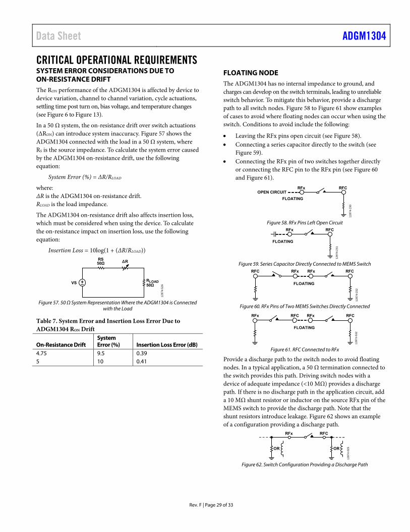
FLOATING NODE The ADGM1304 has no internal impedance to ground, and charges can develop on the switch terminals, leading to unreliable switch behavior. To mitigate this behavior, provide a discharge path to all switch nodes. Figure 58 to Figure 61 show examples of cases to avoid where floating nodes can occur when using the switch. Conditions to avoid include the following:
Leaving the RFx pins open circuit (see Figure 58). Connecting a series capacitor directly to the switch (see
Figure 59). Connecting the RFx pin of two switches together directly
or connecting the RFC pin to the RFx pin (see Figure 60 and Figure 61).
RFx RFC
FLOATING
OPEN CIRCUIT
1287
4-23
0
Figure 58. RFx Pins Left Open Circuit
RFx RFC
FLOATING
1287
4-23
1
Figure 59. Series Capacitor Directly Connected to MEMS Switch
RFx RFC
FLOATING
RFxRFC
1287
4-23
2
Figure 60. RFx Pins of Two MEMS Switches Directly Connected
RFx RFC
FLOATING
RFCRFx
1287
4-53
2
Figure 61. RFC Connected to RFx
Provide a discharge path to the switch nodes to avoid floating nodes. In a typical application, a 50 Ω termination connected to the switch provides this path. Driving switch nodes with a device of adequate impedance (<10 MΩ) provides a discharge path. If there is no discharge path in the application circuit, add a 10 MΩ shunt resistor or inductor on the source RFx pin of the MEMS switch to provide the discharge path. Note that the shunt resistors introduce leakage. Figure 62 shows an example of a configuration providing a discharge path.
RFx
OR OR
RFC
1287
4-02
5
Figure 62. Switch Configuration Providing a Discharge Path

ADGM1304 Data Sheet
Rev. F | Page 30 of 33
Figure 63 and Figure 64 illustrate typical cascaded switch use cases and the corresponding schemes to mitigate floating node risks.
RFCADGM1304 ADGM1304
RF1
RF2
RF3
RF4
RF1
RF2
RF3
RF4
RFC
1287
4-13
3
Figure 63. Two ADGM1304 Devices Connected in Path Selection
Configuration with 10 MΩ Shunt Resistors to Mitigate Floating Nodes
ADGM1304
ADGM1304
ADGM1304RF1
RF2
RF3
RF4
RFC
RF1
RF2
RF3
RF4
RFC
RF1
RF2
RF3
RF4
RFC
1287
4-13
4
Figure 64. Three ADGM1304 Devices Connected in Fanout Configuration
with 10 MΩ Shunt Resistors to Mitigate Floating Nodes
Avoid connecting shunt capacitors directly to the switch. A capa-citor can store a charge and potentially lead to hot switching events when the switch opens or closes if there are no alternative discharge paths. These events affect the cycle lifetime of the switch.
CUMULATIVE ON SWITCH LIFETIME Leaving the switch in an on state for a long period affects the lifetime of the switch because of mechanical degradation effects. These effects can result in the switch failing to turn off. Figure 65 shows a failure rate at 50°C where the mean time to failure is 7.2 years (2628 days), resulting in 50% of the sample lot failing at this point.
99
90
70
FAIL
UR
ES (%
OF
POPU
LATI
ON
)
30
10
110 100 1,000
CONTINUOUSLY ON TIME (DAYS)10,000 100,000
VDD = 3.3V
1287
4-13
7
Figure 65. Cumulative On Switch Lifetime at 50°C, VDD = 3.3 V,
Sample Size = 31 Devices
Temperatures above 50°C further reduce the switch lifetime. The cumulative on switch lifetime specification is also duty cycle dependent. If the user operates the MEMS switch with a duty cycle of less than 50%, the lifetime of the MEMS switch improves.
HANDLING PRECAUTIONS ESD Precautions
All RFx pins of the ADGM1304 pass the following ESD limits:
• 100 V, Class 0 HBM, ANSI/ESDA/JEDEC JS-001-2010 • 500 V, Class C2 FICDM, JEDEC JESD22_C101E
All the RFx pins are rated to 500 V FICDM, making the device safe for automated handling and assembly process. Standard ESD precautions should be taken during manufacturing.
100 V HBM rating of ADGM1304 is susceptible to ESD surge due to human body contact. ESD protection should be added if human body contact is expected.
Electrical Overstress (EOS) Precautions
The ADGM1304 is susceptible to EOS. Therefore, take the following precautions:
• The ADGM1304 is an ESD sensitive device. Ensure to take all of the normal handling precautions, including working only on static dissipative surfaces, wearing wrist straps or other ESD control devices, and storing unused devices in conductive foam.
• Avoid running measurement instruments, such as digital multimeters (DMMs), in autorange modes. Some instruments generate large transient compliance voltages when switching between ranges.
• Use the highest practical DMM range setting (the lowest resolution) for resistance measurements to minimize compliance voltages, particularly during switching.
• Discharge coaxial cables before connecting directly to the switch. Note that coaxial cables can store charge and lead to EOS when directly connected to the switch.
• Avoid connecting large capacitive terminations directly to the switch, as shown in Figure 66. A shunt capacitor can store a charge that potentially leads to hot switching events when the switch opens or closes, affecting the lifetime of the switch.
RFx RFC
1287
4-02
6
Figure 66. Avoid Having a Large Capacitor Directly Connected to the
MEMS Switch

Data Sheet ADGM1304
Rev. F | Page 31 of 33
Mechanical Shock Precautions
The ADGM1304 passes extensive mechanical shock qualification tests, as described in Table 8. These tests validate the robustness of the device when exposed to normal mechanical shocks.
Table 8. Mechanical Qualification Summary Parameter Qualification Mechanical Shock Powered (PMS) IEC 60068-2-27 Random Drop AEC-Q100 Test G5, five drops from
0.6 m Vibration Testing MIL-STD-883, M2007.3, Condition B,
20 Hz to 2000 Hz at 50 g Group D, Sub 4, MIL-
STD-883, M5005 Mechanical shock, 1500 g, 0.5 ms; vibration 50 g sine sweep, 20 Hz to 2000 Hz; acceleration 30,000 g
Do not use the ADGM1304 if dropped. Ensure minimal mechanical shocks during the handling and manufacturing of the device.
Figure 67 shows examples of loose device handling situations to avoid for risk of mechanical shock and ESD events.
1287
4-04
1
NOT RECOMMENDED
DEVICES STORED BULKIN BINS
DEVICE DROPPED
DEVICES DUMPED OUTON BENCHTOP
Figure 67. Situations to Avoid During Handling

ADGM1304 Data Sheet
Rev. F | Page 32 of 33
REGISTER SUMMARY AND DETAILS Table 9. Register Summary Reg Name Bits Bit 7 Bit 6 Bit 5 Bit 4 Bit 3 Bit 2 Bit 1 Bit 0 Reset R/W 0x20 SWITCH_DATA [7:0] INTERNAL_ERROR RESERVED SW4_EN SW3_EN SW2_EN SW1_EN 0x00 R/W
SWITCH DATA REGISTER Address: 0x20, Reset: 0x00, Name: SWITCH_DATA
The switch data register controls the status of the four switches of the ADGM1304.
Table 10. Bit Descriptions for SWITCH_DATA Bits Bit Name Settings Description Reset Access [7:6] INTERNAL_ERROR Internal Error Detection. These bits determine if an internal error has
occurred. 0x0 R
00 No error detected. 01 Error detected. 10 Error detected. 11 Error detected. [5:4] RESERVED Reserved. These bits are reserved. Set these bits to 0. 0x0 R 3 SW4_EN Enable for Switch 4. 0x0 R/W 0 Switch 4 open. 1 Switch 4 closed. 2 SW3_EN Enable for Switch 3. 0x0 R/W 0 Switch 3 open. 1 Switch 3 closed. 1 SW2_EN Enable for Switch 2. 0x0 R/W 0 Switch 2 open. 1 Switch 2 closed. 0 SW1_EN Enable for Switch 1. 0x0 R/W 0 Switch 1 open. 1 Switch 1 closed.

Data Sheet ADGM1304
Rev. F | Page 33 of 33
OUTLINE DIMENSIONS
*EXPOSEDPAD
*EXPOSEDPAD
BOTTOM VIEWTOP VIEW
1
5612
13
1718 24
5.00 BSC
4.00 BSC 2.15 NOM
1.47 NOM
0.16 NOM
0.33 NOM
1.30 NOM
SEATINGPLANE
1.000.950.85
0.300.250.18
0.05 MAX0.02 NOM
0.15 REF
COPLANARITY0.08
PIN 1INDICATOR
0.600.550.50
PIN 1INDICATOR
*FOR PROPER CONNECTION OFTHE EXPOSED PADS, REFER TOTHE PIN CONFIGURATION ANDFUNCTION DESCRIPTIONSSECTION OF THIS DATA SHEET.
0.50BSC
09
-21
-20
11-B
Figure 68. 24-Lead Lead Frame Chip Scale Package [LFCSP_VQ]
5 mm × 4 mm Body, Very Thin Quad (CP-24-9)
Dimensions shown in millimeters
ORDERING GUIDE Model1 Temperature Range Package Description Package Option ADGM1304JCPZ-R2 0°C to 85°C 24-Lead Lead Frame Chip Scale Package [LFCSP_VQ] CP-24-9 ADGM1304JCPZ-RL7 0°C to 85°C 24-Lead Lead Frame Chip Scale Package [LFCSP_VQ] CP-24-9 EVAL-ADGM1304SDZ Evaluation Board 1 Z = RoHS Compliant Part.
©2016–2020 Analog Devices, Inc. All rights reserved. Trademarks and registered trademarks are the property of their respective owners. D12874-0-1/20(F)