
-'Um AD 29 155 - Defense Technical Information Center ENGINEERING REPORT" FOR NAVIGATION RECEIVER...
60
UNCLASSIFIED -'Um AD 29 7 155 ARMEB SERVICES TECHNICAL INFORMAON AGENCY ARLINGTON HALL STATION ARLINGTON 12, VIRGINIA UI 'UNCLASSIFIED
Transcript of -'Um AD 29 155 - Defense Technical Information Center ENGINEERING REPORT" FOR NAVIGATION RECEIVER...

UNCLASSIFIED-'Um
AD 297 155
ARMEB SERVICES TECHNICAL INFORMAON AGENCYARLINGTON HALL STATIONARLINGTON 12, VIRGINIA
UI
'UNCLASSIFIED
NOTICE: When government or other drawings, speci-fications or other data are used for any purposeother than in connection with a definitely relatedgovernment procurement operation, the U. S.Government thereby incurs no responsibility, nor anyobligation whatsoever; and the fact that the Govern-ment may have formulated, furnished, or in any waysupplied the said drawings, specifications, or otherdata is not to be regarded by implication or other-wise as in any manner licensing the holder or anyother person or corporation, or conveying any rightsor permission to manufacture, use or sell anypatented invention that may in any way be relatedthereto.
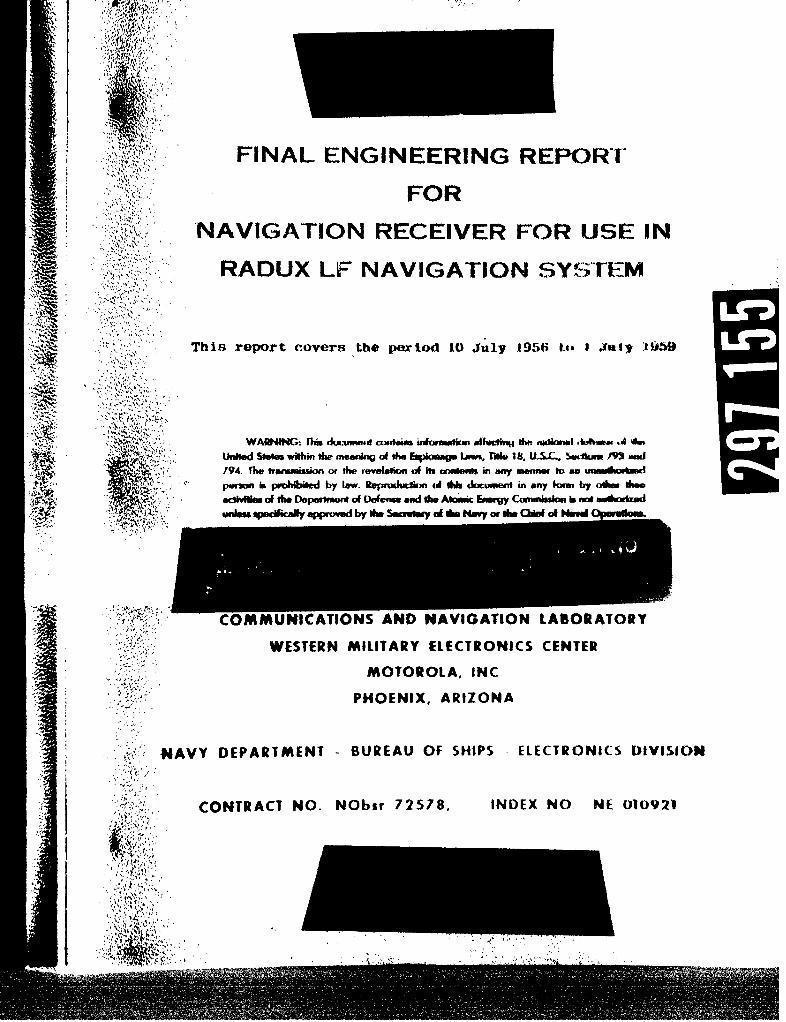
FINAL ENGINEERING REPORT"
FOR
NAVIGATION RECEIVER FOR USE IN
RADUX LF NAVIGATION SYST-EM
This report covers thO pertid 10 July 1956 Lta I Onuly 1059
-0-hed Stefts within the meaning df *h Empioeag Law, Thil 111, U.%CSw au.1a M &rm194. [he trawaision or the reveation of hIf aaefts in any anner to ao waKstuMAbo
perin is prolbiled by law. Reproduction of dub docwwdn in any kwm by otimm dwmeoc**Ilis of the Depesnuent of Defense and the Atoomk Enavry Comwsion b not aw*Aodind
COMMUNICATIONS AND NAVIGATION LABORATORY
WESTERN MILITARY ELECTRONICS CENTER
MOTOROLA, INC
PHOENIX, ARIZONA
NAVY DEPARTMENT -BUREAU OF SHIPS ELECTRONICS DI1VISION
CONTRACT NO. NObsr 72578, INDEX NO NE 010921
41'

IWMEC MOTOROLA PHOENIXControl /~~2 72Copy~s;~
FINAL ENGINEERING REPORT '-FOR
NAVIGATION RECEIVER FOR USE IN
RADUX LF NAVIGAT N SYSTEM
7 1/.5o1fThis report covers the peiiod 10 July 1956 to 1 July 1959
T I A
MAR 1 1963ING. This document contains information affecting the natio nse of the
United States in the meaning of the Espionage Laws, TT .C., Seefio nr79 and .794. The transmission revelation s in any manner to aii unauthorizedperson is prohibited Taw. y r han
activities of the Depart" eense and the nergy Commission is not authorizedp o 4 proved by the Secretary of the Navy or I Operations.
COMMUNICATIONS AND NAVIGATION LABORATORY
WESTERN MILITARY ELECTRONICS CENTER
MOTOROLA, INC.
PHOENIX, ARIZONA
NAVY DEPARTMENT - BUREAU OF SHIPS - ELECTRONICS DIVISION
CONTRACT NO. NObsr 72578, INDEX NO. NE 010921
DISTRIBUTION:
Dept. of the NavyBureau of Ships 25
R. Hoffman 1
A. Hume 1
A. Grimaila 1
J. Kirch 4
H. Kelley 1
TABLE OF CONTENTS
Section Page
ABSTRACT v
PART I, PURPOSE, DATA, AND CONCLUSIONS
PURPOSE ...... ................... .
1.1 DESIGN OBJECTIVES ....... .......... 31.1.1 Receiver ................. 31.1.2 Phase Comparator Unit ..... 4
2 GENERAL FACTUAL DATA ....... ........... 7
2.1 IDENTIFICATION OF PERSONNEL ..... 72.2 PATENTS.. ............ 72.3 REFERENCES ......... .............. 82.4 MEASUREMENT PROCEDURES .............. 8
2.4.1 Shift in Mean ................ 92.4.2 Standard Deviation . . . . . . 92.4.3 Standard Deviation With One-
Microvolt Input ......... .102.4.4 Transient Response ...... 102.4.5 Tracking Test .......... .112.4.6 Sensitivity .. .......... .122.4.7 Omni Test ... ........... ... 132.4.8 Dynamic Range and Maximum Sig-
nal Input ... ........... .. 13
3 DETAILED FACTUAL DATA .. ........... .15
3.1 RECEIVER UNIT ... ............ 153.1.1 Gain Changing Circuits . . .. 15
3.1.1.1 Cathode-CoupledLimiter . . .. . .. 15
3.1.1.2 Switched Gain Control 153.1.1.3 Forward Gain Control 153.1.1.4 Diode Limiters . . .. 16
3.1.2 TRF vs Superheterodyne . . .. 173.1.3 Loop Antenna Coupler ..... 17
3.1.3.1 Grounded Grid Ampli-fier .......... .... 17
3.1.3.2 Cascode Amplifier 173.1.3.3 Untuned Transformer 183.1.3.4 Feedback Amplifier 193.1.3.5 Tuned Loop ...... 203.1.3.6 Operational Amplifier 21
3.1.4 Whip Antenna Coupler ..... 243.1.5 Mixer .... ............. .. 26
*n
010 Oi
TABLE OF CONTENTS (Contd) a
Section Page
3.1.6 Filters .. ........... .273.1.6.1 R-F Filter ..... 273.1.6.2 I-F Filter ..... 273.1.6.3 Local Oscillator
Filter . . . . . . . 283.1.6.4 Low-Pass Filter . 283.1.6.5 Crystal Filter For
Synchronizer . . .. 283.1.7 Discriminator ......... 293.1.8 Receiver Power Supply . . .. 30
3.2 PHASE COMPARATOR UNIT ....... 303.2.1 Phase Detector ....... 303.2.2 Servo Amplifier ....... 313.2.3 Phase Shifter ........ 313.2.4 Fail-Safe Circuits 313.2.5 Local Oscillator ...... 313.2.6 Frequency Divider ...... 333.2.7 Quadrature Coherent Detector. 343.2.8 Commutation Synchronizer . 35
3.2.8.1 Synchronizing UnderPoor S/N Conditions. 36
3.2.8.2 Synchronizer TimeConstant ...... 37 a
3.2.9 Electronic Commutator . . .. 373.2.10 Monitor Oscilloscope . . .. 37
3.3 POWER SUPPLY UNIT ......... 383.4 REMOTE MONITOR UNIT . ........ 383.5 REMOTE INDICATOR UNIT ....... 383.6 RECORDER UNIT ........... 383.7 SEQUENTIAL CORRELATOR ....... 383.8 ELECTROMECHANICAL DATA ....... 39
3.8.1 Servo System . ........ 393.8.1.1 Bandwidth Considera-
tions 393.8.1.2 Servo Stability
Analysis ...... 413.8.2 Motors ................... 433.8.3 Gear Ratio Calculations . . 43
3.8.3.1 Servo Motor to Re-solver, Low Speed 43
3.8.3.2 Servo Motor to Re-solver, High Speed 43
3.8.3.3 Resolver to Counter. 443.8.3.4 Counter to Recorder
Synchro Transmitter. 443.8.3.5 Counter to Remote
Indicator SynchroTransmitter .... 44
4c
TABLE OF CONTENTS (Contd)
Section Page
3.8.3.6 Resolver to LocalOscillator AdjustingCapacitor ...... 44
3.8.4 Mechanical Design Considera-tions ................ 45
3.8.5 Two-Speed Servo System ... 453.8.6 Station Selection ...... 46
3.9 TEST RESULTS ... ............ 463.9.1 Receiver Selectivity and Dy-
namic Range . ......... 463.9.2 Loop Antenna Coupler .... 46
3.9.2.1 Sensitivity 463.9.2.2 Omnidirectional Pat-
tern . ........ 483.9.3 Standard Deviation ...... 483.9.4 Long-Time Stability 483.9.5 Transient Response ...... 483.9.6 Shift in Mean . ........ 483.9.7 Tracking Lag .......... .483.9.8 Synchronization and Readout 49
4 CONCLUSIONS ..... ............... 51
PART II, RECOMMENDATIONS
5 RECOMMENDATIONS .... ............. 52
5.1 MECHANICAL DESIGN .. .......... .525.2 DISCRIMINATOR DESIGN . ........ 52
LIST OF ILLUSTRATIONS
Figure
1 RADUX Navigation Receiver Service Test-Models ............................... 2
2 Shift In Mean Reading Test, Block Diagram. 93 Standard Deviation With One-Microvolt In-
put Test, Block Diagram . ......... 104 Transient Response Test, Block Diagram . 115 Tracking Test, Block Diagram ....... 126 Sensitivity Test, Block Diagram 137 Omni Test, Block Diagram .......... 148 Dynamic Range And Maximum Signal Input
Test, Block Diagram .. ........... 149 Interstage Limiting Circuit, Schematic 16

LIST OF ILLUSTRATIONS (Contd)
Figure Page
10 Basic Antenna Loop Coupler, Block Diagram 1911 Operational Amplifier Input Stage ..... 2112 Equivalent Input Stage . .......... .2113 Capacitor - Coupled Circuit, Schematic . 2414 Transformer - Coupled Circuit, Schematic 2515 Quadrature Coherent Detector Amplifier vs
Phase ...... ................... .3416 Constant-Amplitude Technique ....... 3717 Capacitor Adjustment Methods .. 4418 Two-Speed Servo System Arrangement . . . . 4519 Method of Selecting and Displaying Station
Assignments For Each Line of Position . 47
LIST OF TABLES
Table
1 TECHNICAL PERSONNEL EFFORT ... .. ........ 7
i
iv ~DfDE~frO/AO
JWNHENTE
ABSTRACT
This is the final in a series of reports outlining the design,development, and fabrication of receivers for the Radux LFNavigation equipment for service test evaluation.
Part I, the General and Detailed Factual Data Sections, con-tains both a restatement of the purpose of the project and a de-tailed tabulation of the technical personnel effort expended.
The Detailed Factual Data Section comments on the design anddevelopment work accomplished on the Receiver Unit, Phase Com-parator Unit, Power Supply Unit, Remote Monitor Unit, RemoteIndicator Unit, Recorder Unit, Sequential Correlator, and Elec-tromechanical data. These comments are followed by Test Resultsand a brief Conclusion.
Part II of this report is based on Recommendations for im-provements in mechanical design and discriminator design.
(010N E A v

PART I
PURPOSE, DATA, AND CONCLUSIONS
1. PURPOSE
This contract requires the design, development, and testingof two RADUX navigation receiver service test-models (fig. 1)that are to be evaluated for use in the RADUX LF NavigationSystem. Provisions of Specification SHIPS-N-2207, dated 3January 1956, serve as design criteria for this development.
The equipment is to be used in a hyperbolic phase-comparisonnavigation system to measure the differences in arrival timesof signals from three widely-spaced transmitters. The dif-ference in times of arrivals from paired stations is propor-tional to the difference i.n the distances to each station andlines of constant differences in distance are hyperbolae.These lines of constant difference in distance are called linesof position, and the intersection of two such lines of positionconstitute a navigators fix.
The system is designed to give useful navigational data forranges of 2000 to 3000 miles. The transmitted signals are200-cps frequency modulation with a carrier frequency at ornear 40 kc. The signals are phase locked and measurements aremade on the phase of the modulation. Four separate trans-mitters, operating sequentially, can be accommodated. Thetotal transmission time is 3 seconds with each transmitteroperating for a different period of time.
The primary function of the receiver is to determine thedifference in phase between the pairs of transmitted signals.To accomplish this, the receiver must first properly identifyeach of the transmitted signals and then compare the phase ofeach of the transmitted signals to a locally generated stablesignal. The difference between two such compared signals isthe desired line of position.
Identification of the particular received signal requiresthat the receiver generate a signal sequence that is identicalto the transmitted sequence. For RADUX, this sequence is 7,8, 9, and 10 units with each transmission unit separated by2 off units. Since each unit is 60 milliseconds long, thetotal transmission interval is 3 seconds. The locally generatedsignal sequence is compared to the incoming signal sequence ina series of coincidence gates, and the local sequence is ad-vanced or retarded automatically as required. Once synchro-nized, the local gates are used to switch the incoming signalsto the individual measuring channels at the proper time.

E-4
4)U
oil 14 a*- 410
in0bb
, Op. sew o
RADUX is a precision instrument and in order to provide ac-curate and reliable navigational information, the equipmentmust be capable of making precise measurements under extremelypoor signal to noise ratios and under conditions where sequentialsignals can vary by as much as 100 db.
An important application of this equipment is for submarineoperation under submerged conditions. For this application,reception would be from a crossed loop antenna with extremelysmall signals present. This requires that the receiver circuitsbe highly stable and sensitive and at the same time not intro-duce excessive phase shifts with signal level changes or looporientation. Both of these objectives are attained through theuse of a sharply tuned antenna input circuit followed by anoperational amplifier that serves to flatten the phase responsecharacteristics. Provision is also made for a whip antenna inputfor general purpose and shipboard use.
1.1 DESIGN OBJECTIVES
1.1.1 Receiver
The receiver shall contain one superheterodyne channel capableof receiving frequency-modulated signals on frequencies of 34,36, 38, or 40 kc, with a constant receiver phase delay. Suf-ficient amplification shall be provided to saturate the limiterswith an input of one microvolt or less in an impedance of 50 ohmsto a standard dummy antenna. A liscriminator shall be providedto extract the 200-cps modulation.
The 3-db bandwidth shall be 600 ± 60 cycles with at least60-db attenuation at or more than 2000 cycles away from thecenter frequency. Normal operation shall be obtained with aninput voltage differential up to 100 db with a phase shiftnot exceeding 5 microseconds. Maximum signal input shall be300,000 microvolts.
The loop-antenna coupling circuits in the receiver unit shallmeet the following requirements:
(a) Sensitivity measurements shall be made using ashielded booth and 500-ohm transmission linewith a line constant of 7.75, energized by astandard signal generator over the specifiedfrequency range of 34, 36, 38, and 40 kc. Thesensitivity on omnidirectional operation shallbe 200 microvolts, or less, as indicated by thesignal generator output with the transmissionline connected to obtain a 20-db signal-to-noiserms voltage ratio measured in the 600-cycle re-ceiver bandwidth. The sensitivity on singleplane operation shall be 150 microvolts or lessto provide the same output. The deviation of
0 D1HON D.
the omnidirectional phase pattern from a uni- -form pattern shall not exceed 2 microsecondsat any of the specified frequencies. Meansshall be provided for selecting single-planeloop operation on either of the crossed loopsor for selecting omnidirectional loop opera-tion.
(b) Using a RADUX system signal generator con-nected to the transmission line, a carrierinput of 1000 microvolts for each commutatedsignal shall be applied and the average line-of-position reading noted for each line ofposition. When the carrier of one signal isreduced in 6-db steps so that the signal-to-noise ratio in the receiver bandwidth is one-to-one, the change in the mean of tha associ-ated line of position shall not be more than5 microseconds. A carrier input of 500,000microvolts for each signal shall be appliedand the average line-of-position readingsnoted. When the corrier of one signal isreduced to 50 microvolts in 6-db steps, thechange in the mean of the associated line ofposition shall not be more than 5 microseconds.These requirements apply to both single-planeand omnidirectional operation over the specifiedfrequency range.
1.1.2 Phase Comparator Unit
The navigation-receiver indicator shall be capable of measur-ing the phase difference between the 200-cycle modulation onsignals from a RADUX system signal generator to the accuracyspecified under any of the conditions listed in items (a)through (e). The measurements shall be made on signals withmodulation indices of v/4 (90 degrees total r-f carrier shift).White noise levels shall be equivalent to those obtained froma standard General Radio type 1390A random noise generator ina noise bandwidth of 600 cycles to the 3-db points. The sig-nal and noise voltages shall be mixed in a circuit with a 50-ohmoutput impedance. The mixed signals shall be coupled to theantenna coupler for the whip antenna through a standard dummyantenna.
(a) With 10 microvolts carrier signal and 20 micro-volts rms white noise for one commutated signaland with 200 microvolts and no noise for anothercommutated signal, the standard deviation of120 time-difference readings taken at 30-secondintervals for a 1-hour period shall not exceed10 microseconds.
(b) With 1 microvolt signal input for all four sig-nals and only internally generated noise, thestandard deviation of 240 readings on eachline of position, taken at 6-minute intervalsfor a 24-hour period, shall not exceed 5 micro-seconds.
(c) With 10 microvolts signal input for each sig-nal, the receiver indicator shall follow a30-microsecond instantaneous change in phaseof one signal such that at least 70 percent ofthe change shall be corrected in one minute.
(d) With a signal input of 10 microvolts for onesignal and 200 microvolts for another, thechange in the mean indicated-time-differencereadings shall not exceed 5 microseconds whena white-noise signal of 20 microvolts is addedto the input signals.
(e) Under conditions simulating the receiver in-dicator in motion along the baseline of twotransmitters at a 40-knot rate, the mean lagerror in the indicated phase difference be-tween typical pulsed input signals of 10 micro-volts, with a noise input of 10 microvolts, shallnot exceed 10 microseconds.
A coherent r-f phase detector shall be incorporated in thisunit to distinguish between signal and noise in the i-f outputof the receiver unit. The output of this circuit shall be ap-plied to a cross-correlating commutation synchronizer. Thissynchronizer shall provide an error-voltage output to precessan electronic commutator bringing it into coincidence with thesignal sequence pattern when any two of the four possible sig-nals are received. The time spent in synchronizing the com-mutation shall not exceed 3 minutes when the signal-to-noiseratio in the receiver bandwidth exceeds 1 to 5. The total timerequired for synchronization and phase matching of the receivershall not exceed 15 minutes, starting from a cold start (i.e.,with the equipment warmed up only).
2. GENERAL FACTUAL DATA
2.1 IDENTIFICATION OF PERSONNEL
Technical personnel whose efforts were expended on the problemare listed in Table 1.
TABLE 1
TECHNICAL PERSONNEL EFFORT
Name Title Hours
James Kirch Project Engineer 2094Willis Steen Project Engineer 1784Bernard Parmet Staff Engineer 341George Monser Staff Engineer 304Morton Stern Electrical Engineer 1734Robert Hansen Electrical Engineer 1066Warren Palmer Electrical Engineer 3969Stanley Malinowski Electrical Engineer 573John Corkill Electrical Engineer 911Frederic Harris Electrical Engineer 1809Jack Niebell Electrical Engineer 424John Barto Electrical Engineer 2556John Knudsen Mechanical Engineer 1064David Mocsny Mechanical Engineer 331Theodore Kappel Engineering Aus't 2977Earl Willis Technician 3507Ronald Petz Technician 1293Steve Wronski Technician 1064Rudy Brabec Technician 504Lawrence Tonics Technician 144Charles Hurt Technician 382Patrick Galbraith Technician 2408Richard Netzel Mechanical Designer 2970Arthur Burton Mechanical Designer 1602Ronald Hawkins Mechanical Designer 777
2.2 PATENTS
A method of obtaining maximum available sensitivity from anantenna with a minimum transfer phase slope has been devised byWarren Palmer and Bernard Parmet. The new method eliminates theneed for a large, high-loss input transformer by replacing itwith a light-weight, low-loss, non-critical circuit with proper-ties approaching those of an ideal transformer while minimizingcoupling losses from the antenna to the receiver. An operationalfeedback amplifier is used in conjunction with a tuned antenna torealize these properties.
Patent application presently is being processed by Muellerand Aichele, 105 West Adams Street, Chicago, Illinois.
00MOENFO/D7

2.3 REFERENCES
The following is a list of references cited in portions ofthis report. The order in which each reference appears in thislist does not necessarily reflect the chronological order of ap-pearance in the text but rather acquaints the reader with thereference titles. Footnotes are used to indicate the particularreference cited in the text.
Argiumbau, L. B., Vacuum Tube Circuits, New York:John Wiley & Sons, Inc., 1948.
Chestnut, Harold and R. W. Mayer, Servomechanisms andRegulating System Design, New York: John WileyaSons, Inc., 1952.
Ertman, R. J., Investigation of Underwater Radio Reception,Naval Research La oratorie-, Washingtoiin-D ., Report No.4406, 1954.
Gray, Truman S., Applied Electronics, New York: John Wiley& Sons, Inc., 1954.
Harrington, J. V., "An Analysis of the Detection of RepeatedSignals in Noise by Binary Integration", IRE Trans-actions on Information Theory, March, l953-_V5TTI-!.
Interim Engineering Report No. 18 For Navigation ReceiverFor Use In RADUX LF Nviation stem, Motorola, Inc.,Contract-No.- sr--72578, March, 1959 (Confidential).
Reference Data for Radio Engineers, Fourth Edition,New York: Iternational Telephone and TelegraphCorp., 1956.
Report On Noise In FM Systems and Loop Sensitivit In-RAD y 3stem, Sperry Gyroscope Co., Publicat on-o.372T9,7 ctober, 1955 (Confidential).
Sturley, K. R., Radio Receiver Design, Second Edition,New York: Jo-WiTey &Sons-,Tnc., 1953.
Truxal, John G., Control System Synthesis, New York:McGraw-Hill Book Company, Inc., 1955.
2.4 MEASUREMENT PROCEDURES
The following subparagraphs describe the various test pro-cedures performed on the RADUX navigation receivers. The onlytest equipments required are a General Radio type 1390A randomnoise generator and two Hewlett-Packard type 400C vacuum-tubevoltmeters.
8 DUDAI
2.4.1 Shift In Mean (fig. 2)
The simulator supplies 10 microvolts of signal during the Aand C transmission periods and 200 microvolts of signal duringthe B and D transmission periods. The STATION SELECTOR switchon the RADUX phase comparator is placed in the ABC position. TheRADUX equipment is synchronized and a 15-minute period is used topermit the phase indicator system to null completely. The meanreading (Xo) is taken after the 15-minute null period.
SIMULATOR
A RADUX RECEIVER
IVOLTS
Iv°0 A B UNI -P 0CMAAO
Figure 2. Shift In Mean Reading Test, Block Diagram
The noise generator is then turned on with the amplitude(previously adjusted) producing a 20-microvolt input in a 600-cpsbandwidth. Readings are taken for 75 minutes at 1/2-minute in-tervals. The first 15-minutes' readings are not used in thecalculations; however, the last 60-minutes' readings are addedtogether and divided by the total number of readings (120 in all)to find the average mean reading (Xo).
The shift in mean reading (Xs) is the difference between theaverage mean reading with noise (Xo) and the original mean read-ing before noise was added (Xo), i.e.,
0 = X - Xo (1)
2.4.2 Standard Deviation
The Standard deviation () is calculated from the followingformula, using the same 60-minutes' readings used to calculate
togthe an dvidd b t e tl ubr fradns 10inal

the mean reading:
O= =l(Xi-X°) 2 (2)
where:
X i = any single reading and
n - total No. of readings.
2.4.3 Standard Deviation With One-Microvolt Input (fig. 3)
The simulator supplies a 1-microvolt signal to the RADUX equip-ment with only receiver noise present. The RADUX equipment issynchronized and a 15-minute waiting period is allowed to sta-bilize the initial phase reading. Readings are then taken at6-minute intervals for each line-of-position over a 24-hourperiod (240 readings in all). The standard deviation for eachline-of-position is calculated from equation (2) in respect tothe mean reading over the 24-hour period, i.e., n = 240.
RADUX RECEIVER
SIMULATOR F
1 p VOLT UNIT COMPARATOR
Figure 3. Standard Deviation With One-Microvolt Input Test,Block Diagram
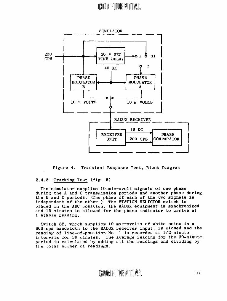
2.4.4 Transient Response (fig. 4)
The simulator supplies lO-microvolt signals of one phaseduring the A and C transmission periods and another phase duringthe B and D periods. (The phase of each of the two signals isindependent of the other.) The STATION SELECTOR switch isplaced in the ABC position, the RADUX equipment is synchronizedand 15 minutes is allowed for the phase indicator to indicatethe phase-difference readings.
The phase of the 200-cps modulated signals is changed rapidlyby 30 microseconds and the reading of line-of-position No. 1(A-B) is recorded at 10-second intervals for 2 minutes. The
time required by the phase indicators to correct 70 percent ofthe phase change (21 microseconds) is the test result.
10 ~ ~ ~ /D
SIMULATOR
CPS TIME DELAY| I S
40 KC ?2
MODULATOR MODULATOR
I0 VOLTS i0 11 VOLTS
RADUX RECEIVER
RECEIVER COMPARATORUNIT 200 CPS OPR
Figure 4. Transient Response Test, Block Diagram
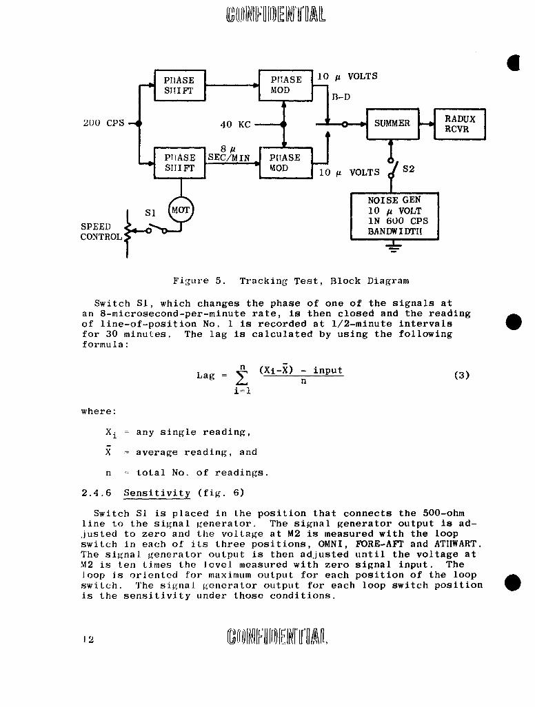
2.4.5 Tracking Test (fig. 5)
The simulator supplies lO-microvolt signals of one phaseduring the A and C transmission periods and another phase duringthe B and D periods. (The phase of each of the two signals isindependent of the other.) The STATION SELECTOR switch isplaced in the ABC position, the RADUX equipment is synchronizedand 15 minutes is allowed for the phase indicator to arrive ata stable reading.
Switch S2, which supplies 10 microvolts of white noise in a600-cps bandwidth to the RADUX receiver input, is closed and thereading of line-of-position No. 1 is recorded at 1/2-minuteintervals for 30 minutes. The average reading for the 30-minuteperiod is calculated by adding all the readings and dividing bythe total number of readings.
200 CPS 40 KC SUMMER RCVR
SPEEDy
PTIASE SEC/miN JPI IASESHIF MOD10 VOLTS $S2
1 NOI SE GEN
Sl MO 10 ju VOLT
SPEE -071N 600 CPS
CONTRO BANDW I DTIITCONTROL.'_0
Figure 5. Tracking Test, Block Diagram
Switch Si, which changes the phase of one of the signals atan 8-microsecond-per-minute rate, is then closed and the readingof line-of-position No. 1 is recorded at 1/2-minute intervalsfor 30 minutes. The lag is calculated by using the followingformula:
n (XI-X) - input (3)Lag =
ni=l
where:
X i = any single reading,
X= average reading, and
n = total No. of readings.
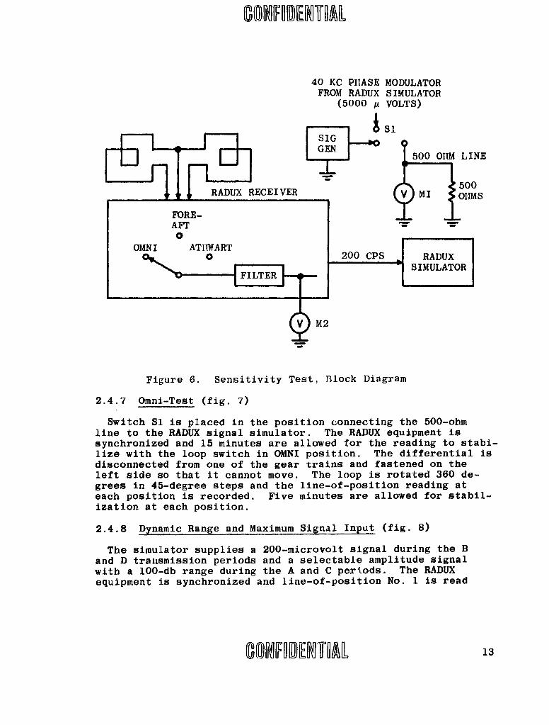
2.4.6 Sensitivity (fig. 6)
Switch S1 is placed in the position that connects the 500-ohmline to the signal generator. The signal generator output is ad-justed to zero and the voltage at M2 is measured with the loopswitch in each of its three positions, OMNI, FORE-AFT and ATHWART.The signal generator output is then adjusted until the voltage atM2 is ten times the level measured with zero signal input. Theloop is oriented for maximum output for each position of the loopswitch. The signal generator output for each loop switch positionis the sensitivity under those conditions.
12 ~(JI1r If~O~1
40 KC PHASE MODULATORFROM RADUX SIMULATOR
(5000 VOLTS)
GEN 500 OH1M LINE
line tECEIVER T R U e u p nt i
FORE- -
OMNI ATI.iART FILTER 00 CPS RADUX_ ' SIMULATOR
Figure 6. Sensitivity Test, Block Diagram
2.4.7 Omni-Test (fig. 7)
Switch S1 is placed in the position connecting the 500-ohmline to the RADUX signal simulator. The RADUX equipment is
synchronized and 15 minutes are allowed for the reading to stabi-lize with the loop switch in OMNI position. The differential isdisconnected from one of the gear trains and fastened on theleft side so that it cannot move. The loop is rotated 360 de-grees in 45-degree steps and the line-of-position reading ateach position is recorded. Five minutes are allowed for stabil-ization at each position.
2.4.8 Dynamic Range and Maximum Signal Input (fig. 8)
The simulator supplies a 200-microvolt signal during the Band D transmission periods and a selectable amplitude signalwith a 100-db range during the A and C periods. The RADUXequipment is synchronized and line-of-position No. 1 is read
1001 DN A 13

RADUX RECEIVER SIMULATOR-i 77-FORE- 200 CPSA [1IHAET
OMNI o ATHWART PHASEo COMPARATOR
16 KC UNIT I i i
500 OHM LINE
500 OIMS
Figure 7. Omni Test, Block Diagram
for each signal-level input, which is varied from 3 to 300,000microvolts in 10-db steps. Five minutes are allowed for eachreading following the initial reading.
3 p VOLTS TOSIMULATOR 300,000 A VOLTS RADUX RECEIVER
VOLT 4 X 16 -K-C
I RECEIVER PHASE
200 . -UNIT COMPARATOR
p VOLTS -OL 0
L _ SigalnptTst BlockDia
Figure 8. Dynamic Range And Maximum Signal Input Test, Block Diagram
14 I}IMIMIINYIL

3. DETAIL FACTUAL DATA
3.1 RECEIVER UNIT
The basic receiver design was based on the three principles ofgood receiver design, i.e., (1) separation of the gain and selec-tivity circuits, (2) placement of the selectivity-determining cir-cults as far ahead of the gain circuits as possible (as near aspossible to the antenna without degrading the noise figure), and(3) utilization of filters for determining selectivity rather thanthe conventional interstage-tuned circuits.
3.1.1 Gain Changing Circuits
One of the more severe requirements placed on the receiver isthat it be capable of operating over a dynamic signal range of100 db, i.e., good phase stability is required between two signalsthat can vary in amplitude by as much as 100 db during a singlemeasuring interval (3 seconds). To ensure this operation, near-perfect signal limiters must be inserted in the receiver. Severaltechniques for phase-stable limiting were evaluated during the pro-gram.
3.1.1.1 Cathode-Coupled Limiter
The cathode-coupled limiter requires two triodes per stage. Aninput cathode follower is cathode-coupled to a grounded grid amp-lifier whereupon limiting is affected by over-driving the stage intoits cut-off regions. By properly adjusting circuit parameters,symmetrical clipping may be accomplished. When the signal is tooweak for limiting, the stage acts as an amplifier with typical meas-ured gain values of from 12 to 16 db. In terms of balanced limit-ing and minimum phase shift, this circuit was adequate; but be-cause of the low value of gain it required too many stages.
3.1.1.2 Switched Gain Control
The stage gain of pentode amplifiers was adjusted by changing thebias with a fixed potentiometer. Phase-shift-versus-amplitude testswere made with constant modulation-index f-m signals. Results ofthese tests indicated that differential phase shifts over the 100-db dynamic range can be kept below 10 microseconds. However, a-chievement of this low value of phase shift is dependent upon avery critical adjustment of the potentiometer, which along withthe problem of commutating a different gain control for each in-coming signal, made this solution undesireable.
3.1.1.3 Forward Gain Control
A method of controlling the gain in the foreward direction wasevaluated. In this method, the signal at the plate of each stageis rectified and fed as a negative bias voltage to the succeeding
01DED/A 15
stage. Efficiency of gain control is improved by feeding only aportion of the signal voltage to the grid of the succeeding stage. SThe test receiver, with 6 stages, had a gain of 120 db. With a100-db change in signal level, the output varied only 1 db and thechange in time delay was only 9 microseconds. However, this methodwas abandoned because the recovery time between signals was morethan could be tolerated and the fact that this technique is an openloop one and will require readjustments with different environ-ments.
3.1.1.4 Diode Limiters
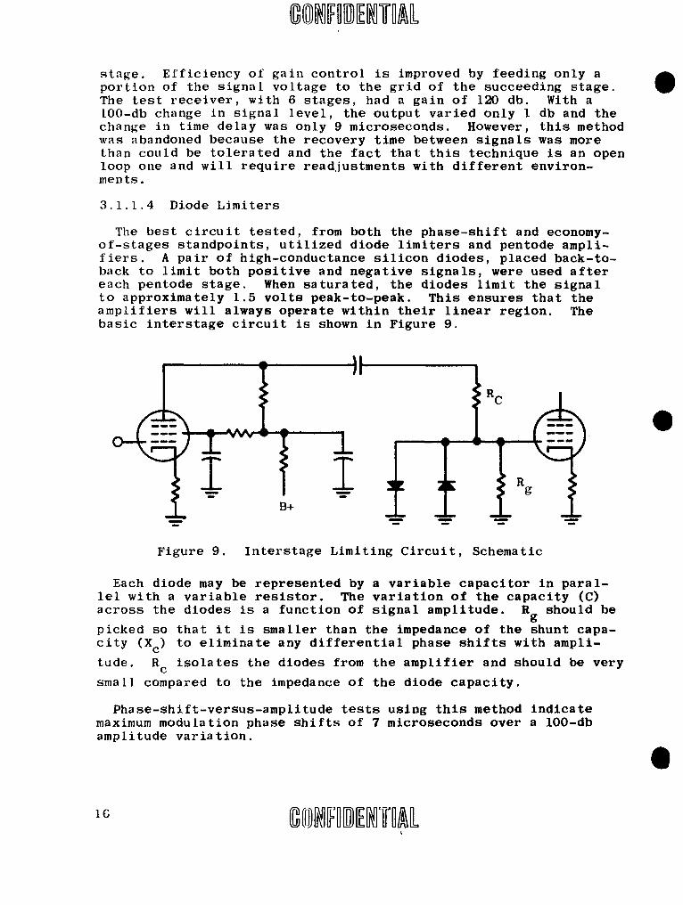
The best circuit tested, from both the phase-shift and economy-of-stages standpoints, utilized diode limiters and pentode ampli-fiers. A pair of high-conductance silicon diodes, placed back-to-back to limit both positive and negative signals, were used aftereach pentode stage. When saturated, the diodes limit the signalto approximately 1.5 volts peak-to-peak. This ensures that theamplifiers will always operate within their linear region. Thebasic interstage circuit is shown in Figure 9.
R
B+ TRFigure 9. Interstage Limiting Circuit, Schematic
Each diode may be represented by a variable capacitor in paral-lel with a variable resistor. The variation of the capacity (C)across the diodes is a function of signal amplitude. R should be
picked so that it is smaller than the impedance of the shunt capa-city (Xc) to eliminate any differential phase shifts with ampli-
tude. Rc isolates the diodes from the amplifier and should be very
small compared to the impedance of the diode capacity.
Phase-shift-versus-amplitude tests using this method indicatemaximum modulation phase shifts of 7 microseconds over a l00-dbamplitude variation.
10
~TA
3.1.2 TRF vs Superheterodyne
A comparative analysis was made to determine whether TRF or super-heterodyne techniques would be better for this development. TheTRF technique offered some advantage in design simplicity since amixer stage would not be required, but this advantage was over-shadowed by the fact that the TRF would require all gain to be atone frequency and it would be extremely difficult to minimize un-wanted feedback. Furthermore, even though both techniques requirefour different coherent signals, the TRF requires that the dis-criminator be retuned when the carrier frequency is changed. As aresult of the analysis, it was decided that the superheterodynetechnique would be best.
3.1.3 Loop Antenna Coupler
It was determined early in the program that the sensitivity andphase shift requirements of the loop input were very stringent andwould require an extensive development program to achieve adequateresults. Thus early development was centered around the use of anuntuned transformer and a low-noise amplifier.
3.1.3.1 Grounded-Grid Amplifier
In an attempt to achieve a minimum noise figure, a high-trans-conductance, type 5842 triode was used as a grounded-grid ampli-fier with an untuned transformer input. Although fairly low e-quivalent noise resistances were achieved for the tube alone, thecombined circuit proved ineffective. Overall sensitivity was poordue to the voltage loss that resulted from matching the relativelyhigh antenna impedance to the low impedance amplifier input.
3.1.3.2 Cascode Amplifier
A'cascode amplifier, that featured low equivalent noise resist-ance and gave good results with the untuned transformer, was de-signed. The basic amplifier is a grounded-cathode-grounded-gridconnection. The grounded-grid stage drastically reduces capaci-tive feedback from output to input without introducing partitionnoise as would be produced in the screen current of a pentode.Shot noise, contributed by the grounded-grid stage, is negligiblebecause of the plate resistance degenerative effect of the grounded-grid stage, that is in series with the cathode of the grounded-gridstage. The noise figure thus approaches the theoretical noise ofthe input section.
This circuit is valuable as a feedback amplifier because of the180-degree relationship between input and output, and also becauseof the high gain. Values of gain between 46 and 54 db were meas-ured for different tubes.
One disadvantage of this arrangement, however, is the large amount
17

of hum produced as a result of the cathode-to-filament rectifica-tion of the grounded-grid section. This effect is caused by thehigh positive voltage on the cathode.
The equivalent noise resistance (R eq) of a triode is approxi-
mated by:
Req 2.5 (4)gm
where:1
gm is the operating transconductance.
The measurement of equivalent noise resistance was accomplishedas follows: the amplifier input was grounded and the amplifieroutput voltage, of a known bandwidth, was measured. The groundwas then removed from the amplifier input, and a signal of suchamplitude as to produce an amplifier output ten times as great asthat obtained with the input grounded was then supplied. Theequivalent noise resistance is found from the equation:
E2
Req - (5)eq 4Ki
where:
En - rms noise voltage,
K - Boltzmann's constant - 1.38 x 10- 23 joules/degree,
T - temperature in degrees Kelvin and
B - noise bandwidth in cycles per second.
Using this method of measurement, the type 6922 cascode amplifierwas found to have 230 ohms equivalent noise resistance, with anoperating transconductance of 12,000 micromhos.
3.1.3.3 Untuned Transformer
A complete analysis was made of the untuned inpul ransformerwith assumptions pertaining to circuit parameters., It was
1 Reference Data For Radio Engineers (New York, 1956) pp
2 Report On Noise In FM Systems And Loop Sensitivity In RADUX
System (Oct oe-F753T,-TConfidenta-T)
Interim Engineering Report No. 18 For Navigation Receiver ForUse In RADUX LF Navigation System (March, 1959). (Confidentia--
18 CO

determined that the best that could be hoped for in terms of thespecification sensitivity was 240 microvolts compared to the re-quired 150 microvolts. Since the specification could not be metwith the untuned transformer, other approaches were investigated.
3.1.3.4 Feedback Amplifier4
Regardless of the antenna coupler input circuit used, a highlystable amplifier is required between the antenna and the r-c couplerphase shifter. It has been shown that the carrier phase shift atthe output of the r-c network is independent of loop orientation
only if the gain and phase shift of each loop circuit is equal.5
Since feedback amplifiers are characterized by an increase in in-put impedance, a decrease in output impedance and a decrease in gaingain changes due to power supply variations and circuit parameters,these properties are used to advantage in the loop antenna coupler.(Refer to Figure 10.) The effect of feedback, then, is to reducethe error caused by gain differences and to lower the output imped-ance of the cathode follower that is driving the r-c coupler cir-cuit.
LO P H COUPLER >C S O EC TO ER P -
LOOP CATHIODE
COUPLER CASCODI FOLLOWER
Figure 10. Basic Antenna Loop Coupler, Block Diagram
4 Truman S. Gray, Applied Electronics (New York, 1954), pp
5 R. J. Ertman, Investigation Of Underwater Radio Reception(Washington D. C.,-1954), pp.
3.1.3.5 Tuned Loop
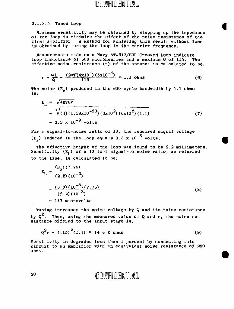
Maximum sensitivity may be obtained by stepping up the impedanceof the loop to minimize the effect of the noise resistance of thefirst amplifier. A method for achieving this result without lossis obtained by tuning the loop to the carrier frequency.
Measurements made on a Navy AT-317/BRR Crossed Loop indicateloop inductance of 500 microhenries and a maximum Q of 115. Theeffective noise resistance (r) of the antenna is calculated to be:
WL (2______10 4 )_(5x10
- 4
r = 1- (2.z4xlO )(5x1.. 11 1.1 ohms (6)
The noise (E n ) produced in the 600-cycle bandwidth by 1.1 ohms
is:
E n = 4v-KTBr
- V(4) (1.38xi0 - 2 3 ) (3x10 2 ) (6x10 2 ) (1.1) (7)
- 3.3 x 10- 9 volts
For a signal-to-noise ratio of 10, the required signal voltage-8(Ea) induced in the loop equals 3.3 x 10 volts. 6The effective height of the loop was found to be 2.2 millimeters.
Sensitivity (EL) of a 10-to-1 signal-to-noise ratio, as referred
to the line, is calculated to be:
(Ea )(7.75)
L -(2.2) (10 - 3
(3.3)(10- 8 )(7.75) (8)
(2.2)(10-3)= 117 microvolts
Tuning increases the noise voltage by Q and its noise resistanceQ2
by Q . Thus, using the measured value of Q and r, the noise re-sistance offered to the input stage is:
Q 2r = (115) 2(1.1) z 14.6 K ohms (9)
Sensitivity is degraded less than 1 percent by connecting thiscircuit to an amplifier with an equivalent noise resistance of 250ohms.
20
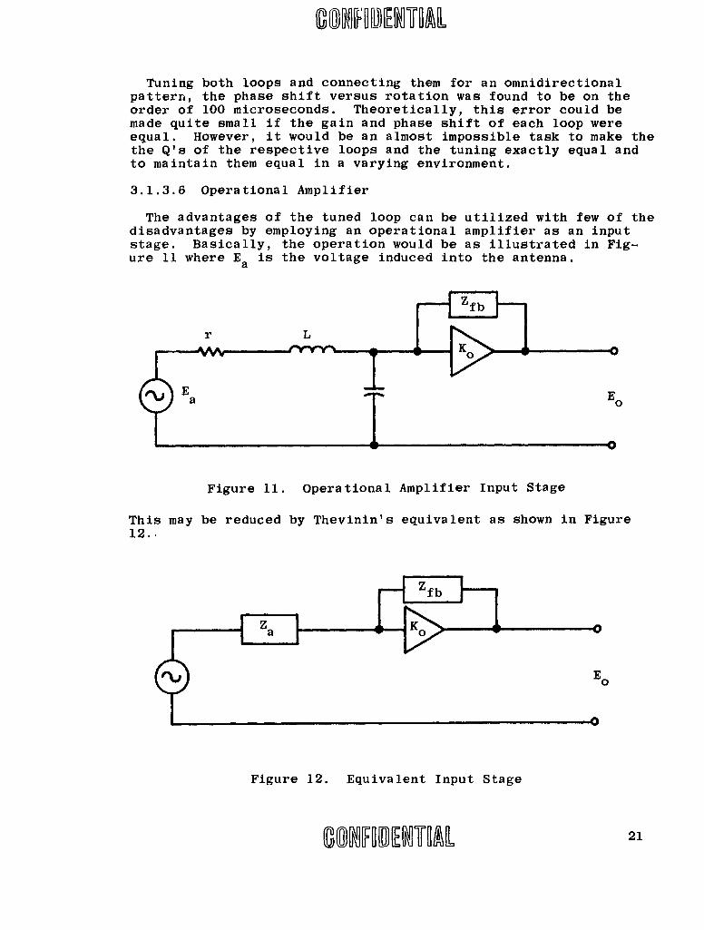
Tuning both loops and connecting them for an omnidirectionalpattern, the phase shift versus rotation was found to be on theorder of 100 microseconds. Theoretically, this error could bemade quite small if the gain and phase shift of each loop wereequal. However, it would be an almost impossible task to make thethe Q's of the respective loops and the tuning exactly equal andto maintain them equal in a varying environment.
3.1.3.6 Operational Amplifier
The advantages of the tuned loop can be utilized with few of thedisadvantages by employing an operational amplifier as an inputstage. Basically, the operation would be as illustrated in Fig-ure 11 where Ea is the voltage induced into the antenna.
Figure 11. Operational Amplifier Input Stage
This may be reduced by Thevinin's equivalent as shown in Figure12..
Z f b '
Figure 12. Equivalent Input Stage
COMMERAL21
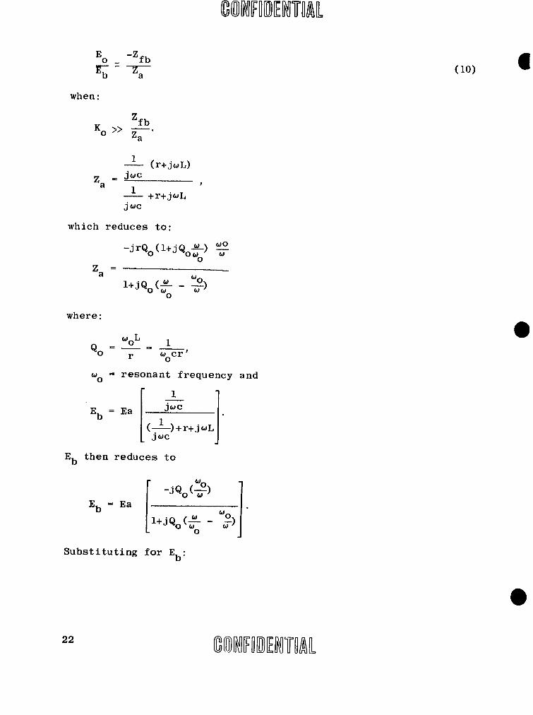
E 0 -Z fb (b - - a(10)
rb Za
when:
ZfbKo z aZa
1 (r+joL)
Za -1JW
1 +r+jwL
jWC
which reduces to:
-jrQ (1+jQo-o) Wo
z =a o1+jQ (- -5)
0
where:
oL 10o r 0o r
-cr
w= resonant frequency and
1
Eb = Ea ,
(--)+r+jwLL jwc JE b then reduces to
0W
Eb = Ea 0 !PI+JQo( -0 - W
u f E0
Substituting for Eb:
22 coo MHOEMAD
UNDDlhO M U /AtM
1 -Q) O
o 0 W
which reduces to
Eo _Z fbE a r(l+jQ --)
0
The phase angle 0 is given by
- -tan-Q (-) (11)
0
when:
Zfb R fb
and the phase slope
-Qo
dO f (12)
Uf 2 21+Q2 ( )0f
0
The maximum phase slope occurs when f = f o i.e.,
-Qo
f
dOl -- radians/cycle (13)
UTff l+Qo Q foIf0 o o
By properly choosing Zfb, the phase slope can be made zero. How-
ever, a resistor was found to work well in this application.
By a similar analysis, the phase slope of the tuned loop withoutfeedback is found to be
D}I IOI YI L23
02Q 6d_ -f- radians/cycle (14)
Since the differential time delay is directly proportional tothe phase slope, a trememdous improvement is achieved by usingfeedback. Test results using this method yielded a sensitivityof 135 microvolts in planar and 190 microvolts in omni and a dif-ferential phase delay of 3 microseconds for 360-degree rotation.
3.1.4 Whip Antenna Coupler
In the analysis that follows, the antenna is assumed to consistof a generator of voltage Ea with an internal impedance Za 6. At
40 kc, this impedance is almost all capacitive; therefore, theassumption is made that Za equals 1/jca .
Because of the 150-foot separation between the antenna and thereceiver, a double-tuned circuit, with the primary at the antenna,is suitable in this application. Two possible configurations con-sidered were (1) capacitance coupling and (2) mutual-inductancecoupling.
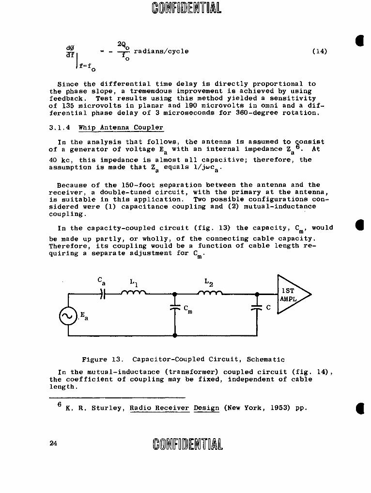
In the capacity-coupled circuit (fig. 13) the capacity, C , would
be made up partly, or wholly, of the connecting cable capacity.Therefore, its coupling would be a function of cable length re-quiring a separate adjustment for Cm .
. Ca L 1 L 2C -
Ea
Figure 13. Capacitor-Coupled Circuit, Schematic
In the mutual-inductance (transformer) coupled circuit (fig. 14),the coefficient of coupling may be fixed, independent of cablelength.
6 K. R. Sturley, Radio Receiver Design (New York, 1953) pp.
24 MUFDNMl 3OIAD
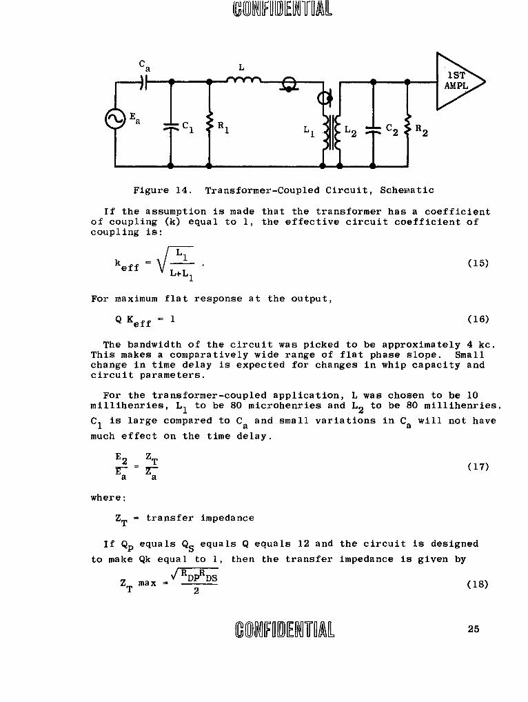
Ca L
0-% 1ST N___T
Figure 14. Transformer-Coupled Circuit, Schematic
If the assumption is made that the transformer has a coefficientof coupling (k) equal to 1, the effective circuit coefficient ofcoupling is:
kef f = (15)L+L 1
For maximum flat response at the output,
Q Keff = 1 (16)
The bandwidth of the circuit was picked to be approximately 4 kc.This makes a comparatively wide range of flat phase slope. Smallchange in time delay is expected for changes in whip capacity andcircuit parameters.
For the transformer-coupled application, L was chosen to be 10millihenries, L1 to be 80 microhenries and L2 to be 80 millihenries.
C1 is large compared to C and small variations in Ca will not have
much effect on the time delay.
E- ZT (17)
a a
where:
ZT = transfer impedance
If Qp equals QS equals Q equals 12 and the circuit is designed
to make Qk equal to 1, then the transfer impedance is given by
ZT max = (18)T 2
where:
RDp - dynamic impedance of primary circuit,
RDS = dynamic impedance of secondary circuit and
ZT -(31 x 10 3 )(2.4 x 10⁵) 5 4.3 x 10⁴ ohmsT 40 kc 2
The noise produced by this circuit in a 600-cps bandwidth, neg-lecting the 1st r-f amplifier noise, is
E n - 4KTR
S (4)(1.38x10 - 2 3 ) (3x1O2) (6xlO )(4.3x1O 4)
- .65 microvolts. (19)
The signal (H2 ) required for a signal-to-noise ratio of 10 is
E2 - 6.5 microvolts. (20)
The voltage (E a ) induced at the antenna for sensitivity:
Ba E2 ZT
= (6) (2xlO4 )
4.3x10⁴
- 2.8 microvolts (21)
By letting Qp approach infinity and changing QS for transitional
coupling, the sensitivity may be improved by 3 db. In this case
E a - (2.8x10)-6(.707) - 2 microvolts (22)
Comparative phase measurements indicate approximately 2 micro-,seconds phase shift attributed to the whip coupler over the 100-dbinput range.
3.1.5 Mixer
A type 6BE6/5750 pentagrid is used as a mixer to change the rfto the 16-kc if. The circuit components were optimized for bestamplitude versus-phase characteristics and conversion gain. Thebest results obtained were with approximately 1.6 volts local-os-cillator drive and 2 volts bias. Under these operating conditions,the conversion gain is approximately 12 db.
26 CONRENflrAo

10 FR EDNEDL
3.1.6 Filters
3.1.6.1 R-F Filter
The r-f filter is a bandpass filter with the following specifi-cations.
(1) Center frequency capable of being switched to 40 and 34 kc.
(2) Minus 3-db bandwidth of 600 ±60 cps.
(3) Minus 60-db bandwidth of not greater than 4000 cycles.
(4) Input impedance (external to the filter) of 10 k.
(5) Output impedance (internal to the filter) of 10 k.
(6) Insertion loss of between 10 and 14 db.
(7) Shift in center frequency of not more than ±20 cps overan operating temperature range of 0 to 70 degrees C.
A major problem encountered in designing this filter was the cor-rection of the time delay differential at the sideband frequencieswith changes in input amplitude. This time delay was consideredto be affected primarily by the inductance changes occurring be-cause of non-linear B-H characteristics of the iron cores used inthe filter. Consequently, the cores were made as large as feas-ible with respect to size and weight.
The differential time delay, with respect to the 100-db inputamplitude change at the f ±200-cps frequency points, was cal-O
culated to be no greater than 2 microseconds. Measurements inthe' system indicate that no more than this amount could be at-tributed to the filter.
3.1.6.2 I-F Filter
The i-f filter is a bandpass filter with the following specifi-cations:
(1) Center frequency of 16 kc.
(2) Minus 3-db bandwidth of ±750 ±10 cps.
(3) Minus 60-db bandwidth of not greater than ±3000 cps.
(4) No flyback above minus 60 db.
(5) Input impedance (external to the filter) of 18 k.
(6) Output impedance (internal to the filter) of 18 k.
U,10R E A 27
(7) Insertion loss no greater than 5 db. i
(8) Shift in center frequency of not more than ±20 cps overan operating temperature range of 0 to 70 degrees C.
The differential time delay, with respect to the 100-db inputamplitude change at the f0 ±200-cps frequency points, was cal-
culated to be no more than 0.5 microseconds.
3.1.6.3 Local Oscillator Filter
The local oscillator filter is a bandpass filter with the fol-lowing specifications:
(1) Center frequency of 52.5 kc.
(2) Three-db bandwiJth of approximately 8 kc.
(3) At least 40 db rejection for frequencies more than ±7 kcaway from the center frequency.
(4) Input impedance of 10 k.
(5) Output impedance of 50 k.
The primary function of the filter is to reject unwanted signalsthat may be produced in the frequency divider and to eliminate any16 kc that may be picked up within the receiver.
3.1.6.4 Low-Pass Filter
The low-pass filter has the following specifications:
(1) Minus 3 db at 500 cps.
(2) Input and output impedances of 10 k.
(3) At least 40 db rejection for frequencies more than 200cps above the cutoff frequency.
This filter is located at the output of the discriminator andhas a bandwidth that is wide enough to pass the effective receivernoise bandwidth. A cutoff frequency of 500 cps was considered tobe wide enough.
3.1.6.5 Crystal Filter For Synchronizer
The crystal filter for the synchronizer has the following speci-fications:
(1) Center frequency of 16 kc ±1 cps.
28 TO D
( S-baEdhf2p
(2) Six-db bandwidth of 12 cps.
(3) Sixty-db bandwidth of 40 cps.
(4) Input and output impedances of 10 k.
(5) Insertion loss of less than 5 db.
(6) Shift in center frequency of not more than ±1 cps overan operating temperature range of from 0 to 60 degreesC.
The bandwidth was made as narrow as the associated rise timewould allow. The rise time causes a shift in the signal pattern;a shift that cannot be so great as to cause the information chan-nel to sample at the wrong time.
3.1.7 Discriminator
At the beginning of the RADUX program, it was decided that co-herent detection did not offer enough improvement over conventionalFoster-Seeley type discriminators. This conclusion was based onNRL report no. 435 and conferences with NEL and NRL personnel.
In the analysis of this system, it was found that the discrimina-tor degraded the signal-to-noise ratio. In the worst case, i.e.,with a signal-to-noise ratio of 1 to 2, the output of the dis-criminator was measured with an approximate signal-to-noise ratioof 1 to 4. The phase detector loop bandwidth was determined fromthe tracking rate required and the worst signal-to-noise ratio tobe encountered. The calculations were based on an input signal-to-noise ratio to the phase detector of 1 to 4 and a maximum phaseerror of 10 microseconds. Improving the signal-to-noise ratio intothe detector, it was found, would not improve the phase accuracymuch as long as the phase detector was operating in a linear region.
The only advantage to coherent detection, therefore, would be theimprovement of the signal-to-noise ratio into the phase detector,which would result in a smaller standard deviation. However, thistype of operation would require separate phase loops, one for eachtransmitting station, and so was not considered practical for thismodel.
Two conventional-type discriminators were tried; the Travis typeand the Foster-Seeley type. It is possible to show that, elec-trically, these circuits are substantially the same.7
The Foster-Seeley discriminator requires a double-tuned trans-former with a fixed coefficient of coupling. A property of
7 L. B. Argiumbau, Vacuum Tube Circuits (New York, 1948) pp.
D,1O~fnEjVOAL 29
COMI[DH A
double -tuned transformers is that the voltage across the tunedstcondary will have a phase angle of 90 degrees relative to thevoiLage across the tuned primary and that the phase of the secon-dary voltage will swing up to plus and minus 90 degrees from this,iti.ht-a.igle relationship as the frequency deviates below or abovethe center frequency. This action changes the fm to an amplitudevariation and is recovered by a peak-detecting circuit resultingin the familiar "S" curve.
The Travis discriminator uses two tuned circuits, one tuned abovethe center frequency and one tuned below it. The action of thiscircuit is to convert the fm to am and then detect the modulationby peak-detecting diodes. The difference between these two out-puts results in the discriminator "S" curve.
The linear region of the "S" curve should be wide enough to passthe receiver noise bandwidth since a narrow linear region couldcause discriminator unbalance under noisy conditions.
Noise balance is critical under poor signal-to-noise ratios.Unbalance can cause excessive shifts in mean when the signal isreduced from good signal-to-noise ratios to poor ones. The majorcause of noise unbalance is the receiver noise bandwidth notbeing symmetrical about the center frequency.
3.1.8 Receiver Power Supply
The receiver power supply is a 250-volt, 150-milliampere regu-lated supply. The output impedance is approximately 1 ohm with nomore than 2 millivolts ripple under full load conditions. The 115volts ac supplied is controlled by the power switch, which islocated on the phase comparator unit.
The power transformer has two 6.3-vac taps for the filaments, a3-amp tap used for the power supply tubes exclusively and a 6-amptap for the receiver tubes.
3.2 PHASE COMPARATOR UNIT
3.2.1 Phase Detector
The basic phase detector is a half-wave, two-diode phase-measuringdevice. This type of detector was chosen because of its simplic-ity and ease of balancing. The average output voltage is zero whenthe received signal is 90 degrees out of phase with the referencesignal and is either positive or negative when the received sig-nal leads or lags the basic 90-degree phase difference. The aver-age d-c output is extracted from the phase detector and developedacross an integrating capacitor.
The integrator is a storage device with its signal applied toone contact of the chopper input to the servo amplifier. An os-cilloscope is used to adjust the average level of the phase
30 OEIDA

detector for zero with no received-signal input.
An undesirable effect of using this technique is that grid cur-rent from the servo-amplifier input stage charges the integratorcapacitor and yields an output error when no actual error exists.However, this effect has been eliminated by applying a voltage,which is equal to the undesired error voltage, to the oppositechopper contact.
3.2.2 Servo Amplifier
The servo amplifier is a conventional amplifier with a push-pulloutput driving a two-phase, servo-motor load. Feedback is employedto reduce the output impedance of the amplifier and to stabilizethe gain. The closed-loop amplifier gain is approximately 2000.The input stage has been designed to minimize grid-current flow.
3.2.3 Phase Shifter
The phase shifter utilizes a precision resolver in conjunctionwith a resistor and capacitor. The resistor is adjusted so thatthe resistance is equal in magnitude to the capacitive reactance.Ideally, the output of the phase shifter is constant in amplitudeand its phase is linearly related to the mechanical rotation ofthe rotor. The resolvers alone contribute a peak-to-peak error of5 microseconds in respect to a perfectly linear relationship be-tween output phase and rotor mechanical rotation.
Linearity tests show that the peak-to-peak error of the shifterstogether with the rest of the phase-measuring loops under staticconditions (i.e., one signal at a time with no time sharing) isapproximately 7 microseconds. The same tests made under dynamic(time sharing) conditions show the peak-to-peak error to be ap-proximately 12 microseconds. The larger errors under dynamic con-ditions are due to cross-coupling between channels.
3.2.4 Fail-Safe Circuits
Fail-safe circuits are provided to indicate correct operationby illuminating the various lamps when the equipment is operatingproperly. The same basic design, consisting of a twin triode anda relay with an adjustment available to obtain circuit operationat the desired error signal amplitude, was used for all circuits.
3.2.5 Local Oscillator
Several local oscillator designs were evaluated and were foundto be lacking in basic stability because of on-off heater controlsbeing used for the crystal oven.
The Manson, precision, one-megacycle oscillator with proportionaloven-temperature control was chosen because it guaranteed that the
r"H OE A 31
long-time drift would not exceed I part in 108 per day. Short-time drift is minimized by the elimination of oven temperaturecycling. Tests on this unit have confirmed long-term drift fig-ures of 3 parts in 109 per day and peak-to-peak short-time driftfigures of approximately 1.5 parts in 109.
An investigation of the results of oscillator drift upon theoperation of the equipment shows that an oscillator with a stabil-ity of 1 part in 108 per day will allow continuous operation with-out automatic frequency control (afc) 10 times longer than a sta-bility of 1 part in 10u. Maximum operating time without using afccan be calculated by letting:
0 = linear range of phase measuring servomechanism = 1.33 de-grees,
e = phase error when tracking at 40 knots along a baseline =
0.33 degrees,and
9 max - maximum allowable phase error.
Then:
@max - OL - 0e (23)
= 1.33 degrees - .33 degrees
0 -- 1 degree.max
Drift is attributed to both long- and short-time components,i.e.,
9max = long time + ashort time* (24)
time = mt2 (25)
where:
m = drift rate in degrees per second per second,and
t - time. (26)
(9 _AT
short time' max
where:
A = peak short-time frequency drift,and
T = period of short-time drift.
0s

Assuming a drift rate of 1 part in 108 per day and a peak short-
timeddrift of 3 parts in 10 9 :
3 36 -8 2m ( G-g7)10 deg/sec
A = (21.6)(10 5 ) deg/sec,and
T = 1800 sec (measured).
Thus, referring to equation (26),
5 3(Oshort time ) (21.6 x 10 - deg/sec)(1.8 x 10 sec) •max
= (12.4)(10-2) deg
= 0.124 deg,
and to equation (24).
9 long time = (max -(0short time )max
= 1 - .124
= .876 deg.
Furthermore, by equation (25):
(tmax) 2 29long time + m
(2)(.876) (4.32) sec 2
(3.6) (10-8)
8 2- (2.1)(10 ) sec
Therefore:
tmax = (1.45)(104) sec
= (2.42)(10 2) min
= 4 hours.
3.2.6 Frequency Divider
The stability, versatility, reliability, ease of adjustment,and maintainability of both sine-wave and the binary feedback-typedividers were considered.
The binary divider is generally superior to the sine-wave typeas far as stability and ease of adjustment are concerned. In both
'CON} OERO 3II

types, however, it is relatively difficult to isolate troubles. 4The sine-wave divider is extremely versatile in that the output
frequencies are relatively easy to change. The fact that the fre-quencies are sine waves makes them easier to handle. Stabilityis adequate for difference-in-phase measurements and reliabilityis very good.
Thus, the sine-wave divider was chosen for its versatility andadequate stability characteristics, which make it adaptable, withonly minor changes, to either a TRF or a superheterodyne receiver.Drift tests of the final sine-wave divider showed a maximum short-time drift rate of only 1 microsecond per minute while temperaturetests on the prototype divider showed it was stable up to 80 de-grees C.
3.2.7 Quadrature Coherent Detector
The quadrature coherent detector is used to extract the ampli-tude envelope of the transmission schedule from the received sig-nal. This envelope is then used to synchronize the local commu-tator.
The detector itself is actually four separate phase detectorswith four reference signals phased in quadrature. The output isthe sum of the outputs of the four phase detectors. The purposeof the quadrature reference signals is to produce a relativelyconstant output regardless of the phase of the signal being de-tected.
Figure 15 shows how the amplitude of the quadrature coherent de-tector varies as the phase of the input signal is varied through
3 db 1.414
0 db 1.000 -
0.000 - 1
00 900 1800 2700 3600 4500 5400
Figure 15. Quadrature Coherent Detector Amplifier vs Phase
34
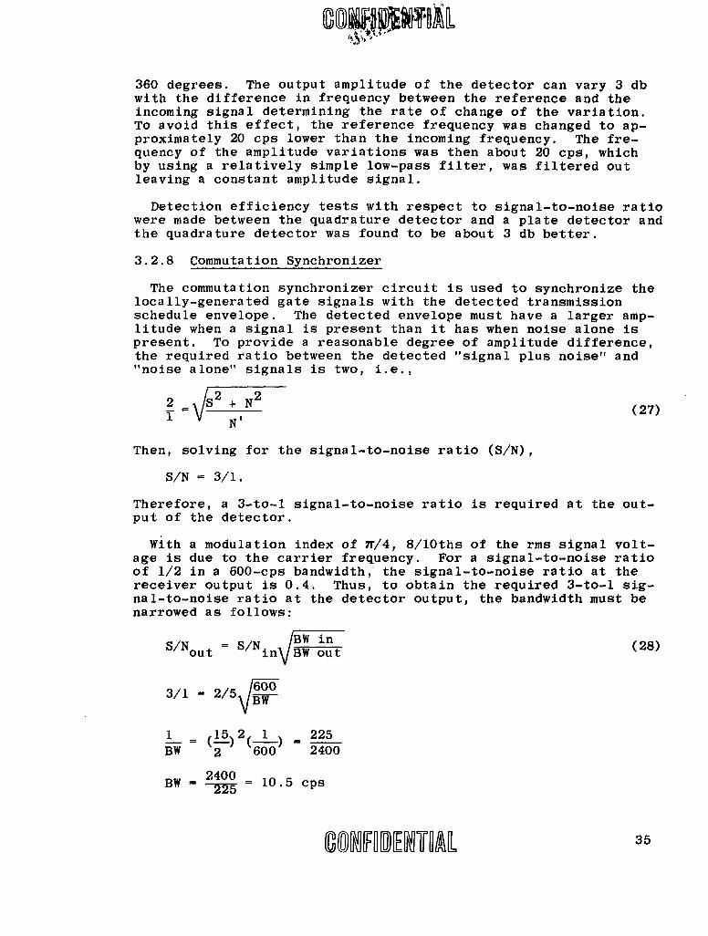
360 degrees. The output amplitude of the detector can vary 3 dbwith the difference in frequency between the reference and theincoming signal determining the rate of change of the variation.To avoid this effect, the reference frequency was changed to ap-proximately 20 cps lower than the incoming frequency. The fre-quency of the amplitude variations was then about 20 cps, whichby using a relatively simple low-pass filter, was filtered outleaving a constant amplitude signal.
Detection efficiency tests with respect to signal-to-noise ratiowere made between the quadrature detector and a plate detector andthe quadrature detector was found to be about 3 db better.
3.2.8 Commutation Synchronizer
The commutation synchronizer circuit is used to synchronize thelocally-generated gate signals with the detected transmissionschedule envelope. The detected envelope must have a larger amp-litude when a signal is present than it has when noise alone ispresent. To provide a reasonable degree of amplitude difference,the required ratio between the detected "signal plus noise" and"noise alone" signals is two, i.e.,
2 2 + 22 =S+ N (27)
Then, solving for the signal-to-noise ratio (S/N),
S/N - 3/1.
Therefore, a 3-to-l signal-to-noise ratio is required at the out-put of the detector.
With a modulation index of ff/4, 8/10ths of the rms signal volt-age is due to the carrier frequency. For a signal-to-noise ratioof 1/2 in a 600-cps bandwidth, the signal-to-noise ratio at thereceiver output is 0.4. Thus, to obtain the required 3-to-i sig-nal-to-noise ratio at the detector output, the bandwidth must benarrowed as follows:
S/N = S/N BW in (28)out inff BWOut
3/1 f 2/5 600
1 (15)2 1 _ 225BW 2 600 2400
BW 2400 = 10.5 cps
M-2-5J~AD

If the signal is passed through a 10.5-cps filter, the S/N out-put should be 3 to 1, which is the minimum required for synchroniz-ing. However, passing the received signals through a 10.5-cpsbandwidth filter at the 16-kc if causes the envelope to have arise time of approximately 100 milliseconds. This rise time dis-torts the incoming envelope and delays it by approximately 100milliseconds causing synchronization to be off by that amount.But, this is not serious since the maximum delay that is tolerablefor proper channeling of the signals to the phase-measuring cir-cuits is 120 milliseconds.
Thus, the narrowest filter usable for synchronization is approxi-mately 10 cps. At the same time, a 10-cps bandwidth has beenshown to reduce a 1-to-2 signal-to-poise ratio in a 600-cps band-width phase-modulated input signal to 3 to 1 at the output. Theseresults lead to the conclusion that the lowest signal-to-noisefiltering is 1 to 2 in a 600-cps bandwidth.
3.2.8.1 Syncironizing Under Poor S/N Conditions
Even through the signal input to the commutation synchronizeris held at a relatively constant level, there is still a differ-ence in signal level under poor signal-to-noise-ratio conditions.This difference is due to the fact that, under noisy conditions,the total level, which includes both signal and noise, is heldconstant and the signal part is at a lower level. 4
A scheme of using agc under poor signal-to-noise-ratio condi-tions was tested but failed to operate properly. This scheme wasunusable for the following reasons:
(1) Response time of the agc would have to be less than 120milliseconds to prevent the synchronization point fromshifting more than 120 milliseconds.
(2) Since response time is less than 120 milliseconds, thenoise gain will automatically be controlled between trans-missions in such manner that will tend to make the averagenoise level as high as the signal level.
(3) Commutated agc is worthless unless synchronization hasalready been accomplished by other means.
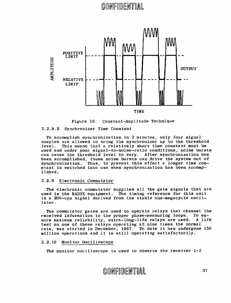
Therefore, a constant-amplitude technique using positive andnegative limiting as shown in Figure 16 was designed.
This system is acceptable unless all stations have a 1-to-1signal-to-noise ratio, at which time the sensitivity is not quiteadequate. A good/poor switch has been incorporated to raise thesignal level during those times when the signal-to-noise ratiois 1-to-1 or worse at all stations.
36
POSITIVELIMIT - -
OUTPUT
S NEGATIVE -.---..
LIMIT
TIME
Figure 16. Constant-Amplitude Technique
3.2.8.2 Synchronizer Time Constant
To accomplish synchronization in 3 minutes, only four signalsamples are allowed to bring the synchronizer up to the thresholdlevel. This means that a relatively short time constant must beused and under poor signal-to-noise-ratio conditions, noise burstscan cause the threshold level to vary. After synchronization hasbeen accomplished, these noise bursts can drive the system out ofsynchronization. Thus, to prevent this effect a longer time con-stant is switched into use when synchronization has been accomp-lished.
3.2.9 Electronic Commutator
The electronic commutator supplies all the gate signals that areused in the RADUX equipment. The timing reference for this unitis a 200-cps signal derived from the stable one-megacycle oscil-lator.
The commutator gates are used to operate relays that channel thereceived information to the proper phase-measuring loops. To en-sure maximum reliability, extra-long-life relays are used. A lifetest on one of these relays operating at nine times the normalrate, was started in December, 1957. To date it has undergone 150million operations and it is still operating satisfactorily.
3.2.10 Monitor Oscilloscope
The monitor oscilloscope is used to observe the receiver i-f
100RENE3

output. In this manner, the operator is able to determine whetheror not the local oscillator is synchronized with the incoming sig-nal. Since the sweep frequency is derived from the local oscil-lator, the pattern will remain stationary only when synchroniza-tion is accomplished.
A synchronizer lamp, which can be selected to light on any de-sired commutator segment, is used in conjunction with the oscillo-scope to evaluate commutator synchronization.
3.3 POWER SUPPLY UNIT
The power supply unit for the phase comparator is contained ina separate case. It is a modified version of circuit No. 3A fromthe Handbook of Preferred Circuits prepared by the National Bureauof Standards. The supply will deliver about 1.5 amperes and theoutput variation is less than ±1 percent for input variations of±10 percent.
3.4 REMOTE MONITOR UNIT
The remote monitor is a separate unit that can be used at a re-mote location to ascertain correct operation of the basic equip-ment. In addition to a monitor oscilloscope, identical to the oneused in the phase comparator, it contains duplicates of all fail-safe lamps and a synchronizer-indicator lamp. The unit is a moni- -tor only and cannot be used to control the main unit.
3.5 REMOTE INDICATOR UNIT
The remote indicator unit indicates the same basic line-of-posi-tion data as the phase comparator unit. It is small in size andcan be used at a remote location to yield the basic position in-formation. It contains synchro receivers coupled to veeder-roottype counters for readout.
3.6 RECORDER UNIT
The navigation recorder is purchased from the Brush InstrumentsDivision of Clevite Corporation. Line-of-position data is derivedfrom synchro transmitters attached to the gear units in the phasecomparator. The recorder has a synchro-receiver input with aservo follower to operate the recorder.
3.7 SEQUENTIAL CORRELATOR
The sequential correlator is a storage device using the theoriesthat noise voltages add as the square root of the sum of the squaresand that signal voltages add algebraically to increase signal-to-noise ratio.8 Storage is accomplished by using a magnetic drum8 J. V. Harrington, "An Analysis of the Detection of Repeated
Signals In Noise By Binary Integration", IRE Transactions OnInformation Theory, (March, 1955), pp.
38 GI DN A
rotating at a constant speed such that one revolution occurs foreach two periods of the RADUX transmission sequence (one revolu-tion per six seconds). Correlation is accomplished by adding suc-ceeding signals to the stored information on the drum. However,the drum speed must be extremely constant and exact so that thesignals will add to the stored information at the proper time.Correlation occurs when the drum speed is synchronized with theincoming signal to be stored. A 400-cps signal, derived from thelocal one-megacycle oscillator, is used to drive a synchronousmotor and gear train coupled to the drum.
Measurements disclosed that drum speed was 2.0944 inches persecond with variations of approximately 1.0472 x 10 -3 sin 6.28tinches per second. As a result, the added signal is always withinplus or minus 35 electrical degrees of the stored signal. Perfectcorrelation will not occur under these conditions, but the correla-tion is good enough to permit signal build-up on the storage medium.
Having established that the drum rotational velocity was adequateto produce correlation, the correlator was tested to determinewhether the magnetic storage drum would add the signals as re-quired. A precision, constant 200-cps signal was used to supplycurrent to the recording head. This signal was derived from thesame 1-mc oscillator as was the 400-cps signal used as the refer-ence for the synchronous motor speed. A read-out head was usedto determine the magnitude of the stored signal and it was ob-served that the signal did not increase with subsequent drum ro-tations. The record current was then doubled and the stored sig-nal level was again observed and found to have doubled also. Thistest verified that the magnetic material was not saturated.
Other tests were made with different amplitudes, and at no timewas a buiId up of stored information observed. The reason for thisis that the magnetic field has the same strength during each appli-cation and the total field in existance on the tape cannot exceedthe strength of the magnetizing force.
Another idea for accomplishing storage was advanced but lack oftime has prevented its instrumentation. In this method, the tapewould be used only as a delay device and the stored signal wouldbe removed from the tape and added externally to the incoming sig-nal. The combined signal would then be re-applied to the tape andstored again. In this manner, the signal could be built up overmany measuring intervals.
3.8 ELECTROMECHANICAL DATA
3.8.1 Servo System
3.8.1.1 Bandwidth Considerations
The indicator bandwidth is specified in terms of the maximum lag
G OIR DNEL 39
at 40 knots and the standard deviation with a l-to-2 signal-to-noise ratio in a 600-cps receiver bandwidth.
The standard deviation (a) is a function of the signal-to-noiseratio in the indicator bandwidth, i.e.,
a= tan - I N/S (29)
For very small angles (less than 3 degrees), the angle in radiansis equal to the tangent of the angle,
o(in radians) = tan I N/S = N/S (30)
The specification requires a maximum standard deviation of 10 micro-seconds, which is 0.72 degrees. Therefore, the signal-to-noiseratio required in the indicator bandwidth is
S/N = 1/a (in radians) (31)
= 180/.72ir
= 79
The discriminator causes approximately 10 db degradation of thesignal-to-noise ratio. The maximum bandwidth of the indicator isthen calculated as follows:
sv mx = J[S/N (in degradation), 2 JBWinput.) (32)(BWservo /N (required.] 2 2
:(1/2)(1/3)] 2= [,/)13 (300) = .0013
79
In calculating the minimum bandwidth for tracking 40 knots, cer-tain factors are considered. For instance, the tracking rate (6)for tracking 40 knots is .068 microseconds per second. The inte-9gration gain (Kv ) of the servo loop is then given by the equation
9
Kv = 4/lag (33)
= 0.68 psec/sec/10 psec
= .0068/sec
With a damping factor (Q) of .707, the minimum bandwidth10 to meetthe tracking rate becomes
Harold Chestnut and R. W. Mayer, Servomechanisms And Regulat-ing System Design (New York, 1952), pp. 216.
10__ _ _ _ _ _ _ _ _ _4John G. Truxal, Control System Synthesis (New York, 1955)pp.293.
40 1 1 -C1}O/D~
BW = Kv/4 (34)
= .0068/.707
= .0096 rad/sec
= .00153 cycles/sec
Since the signal input to the indicator system is sequentiallytime shared, the phase detector output is fed to the "A" channelintegrator when the "A" station signal is present. The error in-formation is stored during the time when the "A" station signal isnot present. Each servo loop then gets its error signal from anintegrator and the phase detector output is sampled sequentiallyonce each 3 seconds by each integrator.
3.8.1.2 Servo Stability Analysis
For the RADUX system the time constant (T1) is 1/2 and the open
loop transfer function G(s), as a function of the complex frequencys, is given by the equation:
G(s)= K _ 2K 2K (35)
s(s + 1/2) s (s + 1/2)
Where:
K = gain
Since the indicator is a sampled-data system, the analysis can
be carried out in the Z plane as followsll1
G*(s) = G(Z) - 2KZ 2KZ_T (36)Z- I Z- e
where:
T = Sample Period
Z STZ = eT
G(Z) = 2KZ (1 - e - T )
(Z - 1)(Z - e - T)
1 + G(Z) - (Z - )(Z - e-T ) + 2 KZ (1 - e - T )
(Z - 1)(Z - e - T)
11 Ibid., pp. 522-524.
COIR ERAL41
O"DHM1NA
The closed loop system is stable if the numerator of I + G(X)possesses no zeros outside the unit circle in the Z plane.
P(Z) = 1 + G(Z) = Z2 + 12K (l-e -T) - eT - i1 Z + e-T (37)
The necessary and sufficient conditions for P(Z) to have no zerosoutside the unit circle are:
IP(O)l < I,IP(l)I > 0IP(-17)I>0.
Applying these three conditions,
P(0) = e-T < 1 (38)
P(l) = 2K(l - e - T) > 0 (39)
P(-l) = 2 - 2K(l - e - T ) + 2 e-T > 0 (40)
The first two conditions are satisfied for any positive gain andthe third condition places an upper bound on K.
T1 2K(l - e - T) < + 2 (e-T + 1) (41)
+ e-T1 - e
The sampling period (T) is 3 seconds, therefore, for the indica-tor system to be stable:
1-3 i+ I-
K < 1 + e e (42)e - -3 i1l-e 1--
e
1+i+ I
1
1 .05
.95
K <I.1
The K of the RADUX indicator system is approximately 0.0136 sothe system is extremely stable.
42 CM OI A
3.8.2 Motors
The motors used in the phase shifter indicator unit are size-15,60-cps, 2-field servo motors. They are integrally mounted on gear-head reducers. The largest speed reduction practical was taken inthe gearhead, which in this case is 77:1.
3.8.3 Gear Ratio Calculations
3.8.3.1 Servo Motor To Resolver, Low Speed
The reduction from the motor to the resolver is 399,259:1. As-suming a motor speed of 2,500 revolutions per minute, the resolverspeed in the unit of measurement would be
2,500 rev/mmn = 0.00625 rev/mmn (43)
399,259
If one resolvei' revolution requires 5,000 microseconds, the resol-ver speed in microseconds per minute becomes
(5,000 psec/rev)(0.00625 rev/min) = 31.25 psec/min (44)
And if furthermore one microsecond is approximately equ.l to0.162 knots, the tracking rate is
(31.25 psec/min)(0.162 knots/psec)(60 min/hr) = 304 knots (45)
the time required to reduce a 200-microsecond error in low speedis approximately
200 psec = 6.4 min (46)
31.25 psec/min
3.8.3.2 Servomotor To Resolver, High Speed
The reduction from the motor to the resolver is 24,954:1 in thehigh-speed condition. This rate is 1/16 the reduction in low speed,therefore the resolver speed in revolutions per minute is
(16) (0.00625 rev/min) = 0.1 rev/min. (47)
The resolver speed in microseconds per minute is
(16) (31.25 psec/min) = 500 pjsec/min (48)
A 2,500-microsecond phase difference will be reduced to 200 micro-seconds in approximately 4.6 minutes, i.e.,
2,300 ,sec 4.6 min (49)
500 ysec/min
3.8.3.3 Resolver To Counter
The reduction from the counter to the resolver is 500:1 with theother input to the differential fixed. The resolver completes onerevolution in 5,000 microseconds while the counter takes 10 micro-seconds.
3.8.3.4 Counter To Recorder Synchro*Transmitter
There is a 40:1 reduction between the counter and the recordersynchro transmitter with one transmitter revolution requiring 400microseconds.
3.8.3.5 Counter To Remote Indicator Synchro Transmitter
The ratio between the counter and the remote indicator synchrotransmitter is 1:1 with one transmitter revolution requiring 10microseconds.
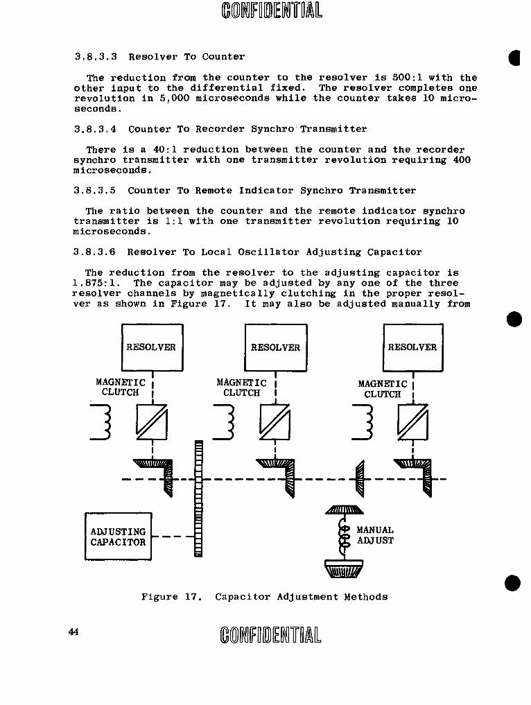
3.8.3.6 Resolver To Local Oscillator Adjusting Capacitor
The reduction from the resolver to the adjusting capacitor is1.875:1. The capacitor may be adjusted by any one of the threeresolver channels by magnetically clutching in the proper resol-ver as shown in Figure 17. It may also be adjusted manually from
RESOLVER RESOLVER RESOLVER
MAGNETIC MAGNETIC I MAGNETIC ICLUTCH I CLUTCH I CLUTCH I
ADJUSTING MANUALCAPACITOR ADJUST
Figure 17. Capacitor Adjustment Methods
44~ED/D

the front panel. Pushing in on the manual adjust control engagesthe control with the adjusting capacitor driving shaft while atthe same time tripping a microswtich that de-energizes all themagnetic clutches.
3.8.4 Mechanical Design Considerations
Becaase the indicator gearing assembly is so complex, maintain-ability was given prime consideration along with accuracy and re-liability. The package consists of three identical gear assembliesmounted as plug-in packages on a frame containing additional com-mon gearing. Since the three gear assemblies are identical, aminimum number of spare parts is required. To facilitate mainten-ance, the entire assembly may be easily removed.
The indicator unit is adequately ruggedized to withstand thevibration and shock expected in Naval service without the gearsbinding or losing accuracy.
3.8.5 Two-Speed Servo System
A two-speed servo system is required to provide rapid rotationof the resolvers during large error periods (error larger than 200microseconds) and slow rotation during operation with relativelysmall errors. The specification requires the high-speed to re-duce a 2500-microsecond phase difference to 200 microseconds with-in 5 minutes. This set the minimum slewing rate at 460 microsec-onds per minute. The specification also requires the low speed totrack a 40-knot rate, which is 4.1 microseconds per minute, whilerequiring less than 15 minutes total receiver synchronization andphase matching time. It was decided that to meet these require-ments, the low-speed must reduce a 200-microsecond phase differ-ence to zero in less than half this period of time, which is arate of greater than 26.7 microseconds per minute.
4:1INVERSEr 1 OUTPUT
GEAR ISHAFTS- HEAD MAGNETIC
CLUTCH 4:1L_ J -44zCOAXIALSHAFTS
Figure 18. Two-Speed Servo System Arrangement
0 F01DEI 45

The present system provides a low speed of approximately 31.25microseconds per minute and a high speed of approximately 500microseconds per minute. The two speeds were derived as shown inFigure 18.
The servo motor drives the input to a magnetic clutch with twooutput shafts. In high-speed operation, one end of the clutch en-gages to provide a 4:1 speed increase. In low-speed operation,the other end of the clutch engages to provide a 4:1 speed re-duction. This arrangement allows the high speed to be 16 timesgreater than the low speed.
3.8.6 Station Selection
The receiver is required to select three of four possible re-ceived signals and to indicate the phase difference between them.The phase difference must be indicated as station I minus station2, station 2 minus station 3 and station 1 minus station 3.
Figure 19 is a table showing the method of selecting and display-ing station assignments for each line of position. The four sta-tions are designated A, B, C and D. A front panel switch selectsany one of the four possible combinations of stations. Proper sig-nals are switched to the resolvers and an indicator below eachcounter displays which two stations are assigned to each line ofposition. To achieve the proper readout, the counter on line ofposition (L.O.P.) number I is reversed from the counters of L.O.P's2 and 3. The resolver of channel 2 is connected to produce an in-creasing phase angle for the same direction of rotation that wouldproduce a decreasing phase angle on channel 1.
3.9 TEST RESULTS
3.9.1 Receiver Selectivity and Dynamic Range
The receiver selectivity requirements, have been met in theirentirety. Dynamic range design objectives have been substantiallymet. Tests on the final units show an expected differential phasedelay of approximately 15 microseconds over a 100-db amplituderange, as compared to the design objective of 5 microseconds.Tests on the breadboard receivers have been made with differentialdelays of 5 or less.
3.9.2 Loop Antenna Coupler
3.9.2.1 Sensitivity
The loop antenna coupler sensitivity requirements have been metin their entirety by using antenna tuning. Sensitivity is 150microvolts with a single loop planar and 200 microvolts withcrossed loops (omni) and the antenna coupler.
46 "ODROENAL

I I 11ME
I 0Do 0
06 C
0
0 14 C4 00 C1;
0 (0
U OU
I iIr~mz -04
I1 ~ ~ I 9 CV Io v I
Imi E.L- III 1-41MM
I Q
E- - -w-W H z . Al
z- M . .rto
R 8 rl~A
3.9.2.2 Omnidirectional Pattern
The differential phase shift with antenna rotation design ob-jectives have essentially been met by using a unique feedbacktechnique in conjunction with the tuned antennas. The differen-tial phase delay measures between 2 and 5 microseconds, althoughtheoretically, it should be much less than one microsecond. Thesevalues are attributed to the inability to adjust the r-c couplingnetwork perfectly with existing adjustment and measurement tech-niques and to receiver long time stability.
3.9.3 Standard Deviation
The standard deviation design objective of 10 microseconds es-sentially has been met with standard deviation figures of between10 and 15 microseconds. This result is the direct consequence ofthe indicator bandwidth.
3.9.4 Long-Time Stability
Long-time stability requires the standard deviation over a 24-hour period to be 5 microseconds or less with a 1-microvolt input.Test results show the requirements to be essentially met with meas-ured standard deviations of between 7 and 13 microseconds under therequired conditions.
3.9.5 Transient Response
The transient response requirements have been met with a meas-ured time of 50 seconds to the 70-percent recovery points as com-pared to the 60-second maximum required by specification. Thetransient response is determined when the bandwidth is fixed. Slow-ing the response narrows the bandwidth, which in turn reduces thestandard deviations under poor signal-to-noise-ratio conditions.
3.9.6 Shift In Mean
The mean reading under a poor signal-to-noise ratio is a func-tion of the discriminator balance as well as the balance of allnoise energy above and below the discriminator center frequency.The shift-in-mean requirements were met by using a trial-and-error method to adjust the shape of the receiver band-pass anddiscriminator balance until the shift was low enough to meet thespecification. This is not adequate because a repeatable methodfor making the necessary adjustments is lacking. A better balanc-ing technique will be needed for future models.
3.9.7 Tracking Lag
Tracking-lag performance tests show that the specification es-sentially has been met. Results show a lag of approximately 15microseconds compared to the design goal of 10 microseconds. Thelag is determined by indicator bandwidth.
48 COMHOEDEAL

3.9.8 Synchronization And Readout
The requirements of a 3-minute synchronization time and a read-out within 15 minutes from an unsynchronized condition have beenmet. The goal of synchronizing with two stations with 1-to-5signal-to-noise ratios has not and cannot be met with the techni-ques used in this equipment. Synchronizing with 4 stations underl-to-3 signal-to-noise-ratio conditions has been accomplished witha high degree of probability.

1 4. CONCLUSIONS
From the test results it can be seen that the equipment de-livered by Motorola under this contract substantially meetsthe performance specifications.
An invention has made possible the advance of the state-of-the-art to the point where the specification sensitivity re-quirements were met together with the requirement that themeasured phase of a signal be independent of the loop antennaorientation.
51.
PART II
RECOMMENDATIONS
5. RECOMMENDATIONS
The equipment developed under this contract is believed tobe adequate electrically for performing the tasks required ofit. A few exceptions, however, are discussed in the followingparagraphs.
5.1 MECHANICAL DESIGN
A mechanical redesign of the receiver would be desirableto minimize interference caused by layout deficiencies. Afinal design, to be produced in large quantities, should bemade with power-consumption and size reductions as prime ob-jectives.
5.2 DISCRIMINATOR DESIGN
A new discriminator design would be required with a means ofnoise balancing as an inherent part of the circuit. If pos-sible, an automatic arrangement should be used.
/