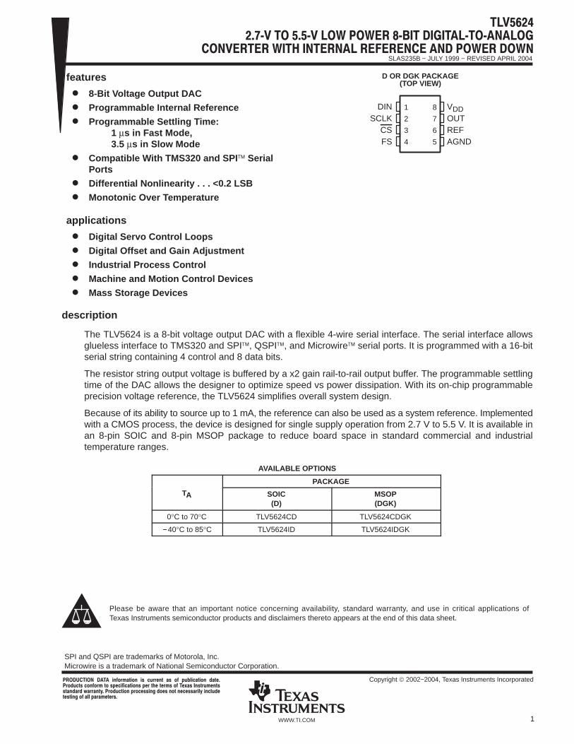
˘ ˇ - ti.com · ˘ ˇ SLAS235B − JULY 1999 − REVISED APRIL 2004 2 functional block diagram...
23
TLV5624 2.7ĆV TO 5.5ĆV LOW POWER 8ĆBIT DIGITALĆTOĆANALOG CONVERTER WITH INTERNAL REFERENCE AND POWER DOWN SLAS235B - JULY 1999 - REVISED APRIL 2004 1 WWW.TI.COM features D 8-Bit Voltage Output DAC D Programmable Internal Reference D Programmable Settling Time: 1 µs in Fast Mode, 3.5 µs in Slow Mode D Compatible With TMS320 and SPI Serial Ports D Differential Nonlinearity . . . <0.2 LSB D Monotonic Over Temperature applications D Digital Servo Control Loops D Digital Offset and Gain Adjustment D Industrial Process Control D Machine and Motion Control Devices D Mass Storage Devices description The TLV5624 is a 8-bit voltage output DAC with a flexible 4-wire serial interface. The serial interface allows glueless interface to TMS320 and SPI, QSPI, and Microwire serial ports. It is programmed with a 16-bit serial string containing 4 control and 8 data bits. The resistor string output voltage is buffered by a x2 gain rail-to-rail output buffer. The programmable settling time of the DAC allows the designer to optimize speed vs power dissipation. With its on-chip programmable precision voltage reference, the TLV5624 simplifies overall system design. Because of its ability to source up to 1 mA, the reference can also be used as a system reference. Implemented with a CMOS process, the device is designed for single supply operation from 2.7 V to 5.5 V. It is available in an 8-pin SOIC and 8-pin MSOP package to reduce board space in standard commercial and industrial temperature ranges. AVAILABLE OPTIONS PACKAGE T A SOIC (D) MSOP (DGK) 0°C to 70°C TLV5624CD TLV5624CDGK -40°C to 85°C TLV5624ID TLV5624IDGK Please be aware that an important notice concerning availability, standard warranty, and use in critical applications of Texas Instruments semiconductor products and disclaimers thereto appears at the end of this data sheet. Copyright 2002-2004, Texas Instruments Incorporated PRODUCTION DATA information is current as of publication date. Products conform to specifications per the terms of Texas Instruments standard warranty. Production processing does not necessarily include testing of all parameters. 1 2 3 4 8 7 6 5 DIN SCLK CS FS V DD OUT REF AGND D OR DGK PACKAGE (TOP VIEW) SPI and QSPI are trademarks of Motorola, Inc. Microwire is a trademark of National Semiconductor Corporation.
Transcript of ˘ ˇ - ti.com · ˘ ˇ SLAS235B − JULY 1999 − REVISED APRIL 2004 2 functional block diagram...
SLAS235B − JULY 1999 − REVISED APRIL 2004
1WWW.TI.COM
features
8-Bit Voltage Output DAC
Programmable Internal Reference
Programmable Settling Time:1 µs in Fast Mode,3.5 µs in Slow Mode
Compatible With TMS320 and SPI SerialPorts
Differential Nonlinearit y . . . <0.2 LSB
Monotonic Over Temperature
applications
Digital Servo Control Loops
Digital Offset and Gain Adjustment
Industrial Process Control
Machine and Motion Control Devices
Mass Storage Devices
description
The TLV5624 is a 8-bit voltage output DAC with a flexible 4-wire serial interface. The serial interface allowsglueless interface to TMS320 and SPI, QSPI, and Microwire serial ports. It is programmed with a 16-bitserial string containing 4 control and 8 data bits.
The resistor string output voltage is buffered by a x2 gain rail-to-rail output buffer. The programmable settlingtime of the DAC allows the designer to optimize speed vs power dissipation. With its on-chip programmableprecision voltage reference, the TLV5624 simplifies overall system design.
Because of its ability to source up to 1 mA, the reference can also be used as a system reference. Implementedwith a CMOS process, the device is designed for single supply operation from 2.7 V to 5.5 V. It is available inan 8-pin SOIC and 8-pin MSOP package to reduce board space in standard commercial and industrialtemperature ranges.
AVAILABLE OPTIONS
PACKAGE
TA SOIC(D)
MSOP(DGK)
0°C to 70°C TLV5624CD TLV5624CDGK
−40°C to 85°C TLV5624ID TLV5624IDGK
Please be aware that an important notice concerning availability, standard warranty, and use in critical applications ofTexas Instruments semiconductor products and disclaimers thereto appears at the end of this data sheet.
Copyright 2002−2004, Texas Instruments Incorporated !"# $ %&'# "$ (&)*%"# +"#' +&%#$ %! # $('%%"#$ (' #,' #'!$ '-"$ $#&!'#$$#"+"+ .""#/ +&%# (%'$$0 +'$ # '%'$$"*/ %*&+'#'$#0 "** (""!'#'$
1
2
3
4
8
7
6
5
DINSCLK
CSFS
VDDOUTREFAGND
D OR DGK PACKAGE(TOP VIEW)
SPI and QSPI are trademarks of Motorola, Inc.Microwire is a trademark of National Semiconductor Corporation.
SLAS235B − JULY 1999 − REVISED APRIL 2004
2 WWW.TI.COM
functional block diagram
SerialInterface
andControl 8-Bit
DACLatch
CS
DIN
OUT
Power-OnReset
x28
2-BitControlLatch
2
Powerand Speed
Control
2
VoltageBandgap
PGA WithOutput Enable
8
REF
FS
SCLK
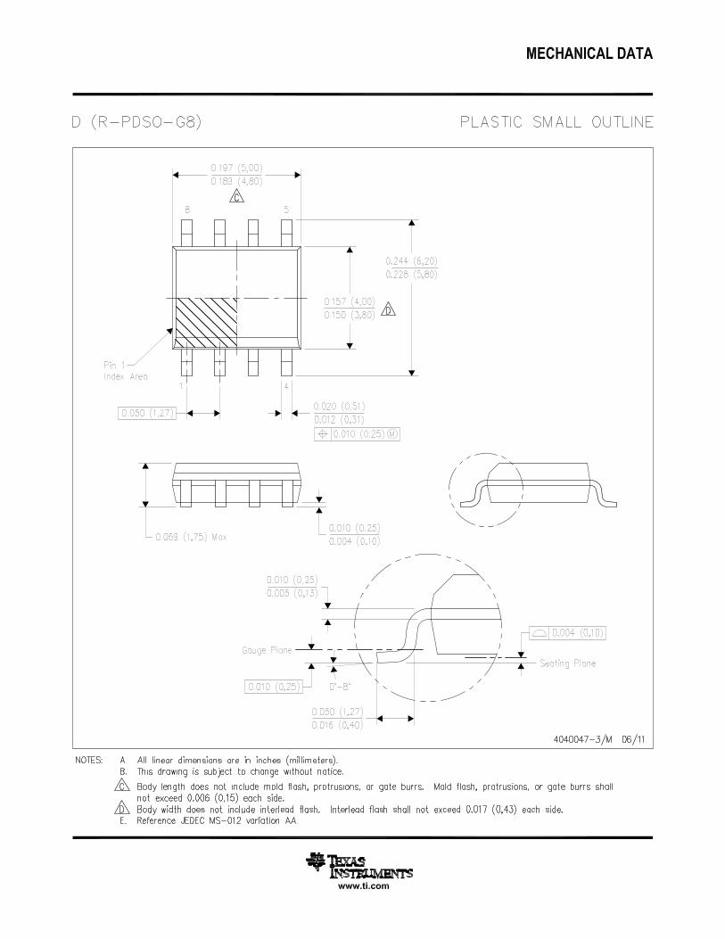
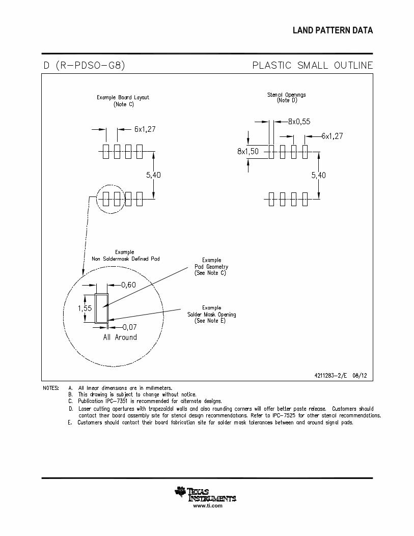
Terminal Functions
TERMINALI/O/P DESCRIPTION
NAME NO.I/O/P DESCRIPTION
AGND 5 P Ground
CS 3 I Chip select. Digital input active low, used to enable/disable inputs
DIN 1 I Digital serial data input
FS 4 I Frame sync input
OUT 7 O DAC A analog voltage output
REF 6 I/O Analog reference voltage input/output
SCLK 2 I Digital serial clock input
VDD 8 P Positive power supply
SLAS235B − JULY 1999 − REVISED APRIL 2004
3WWW.TI.COM
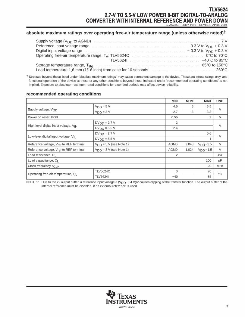
absolute maximum ratings over operating free-air temperature range (unless otherwise noted) †
Supply voltage (VDD to AGND) 7 V. . . . . . . . . . . . . . . . . . . . . . . . . . . . . . . . . . . . . . . . . . . . . . . . . . . . . . . . . . . . . . . Reference input voltage range − 0.3 V to VDD + 0.3 V. . . . . . . . . . . . . . . . . . . . . . . . . . . . . . . . . . . . . . . . . . . . . . . Digital input voltage range − 0.3 V to VDD + 0.3 V. . . . . . . . . . . . . . . . . . . . . . . . . . . . . . . . . . . . . . . . . . . . . . . . . . Operating free-air temperature range, TA: TLV5624C 0°C to 70°C. . . . . . . . . . . . . . . . . . . . . . . . . . . . . . . . . . . .
TLV5624I −40°C to 85°C. . . . . . . . . . . . . . . . . . . . . . . . . . . . . . . . . . . Storage temperature range, Tstg −65°C to 150°C. . . . . . . . . . . . . . . . . . . . . . . . . . . . . . . . . . . . . . . . . . . . . . . . . . . Lead temperature 1,6 mm (1/16 inch) from case for 10 seconds 260°C. . . . . . . . . . . . . . . . . . . . . . . . . . . . . . .
† Stresses beyond those listed under “absolute maximum ratings” may cause permanent damage to the device. These are stress ratings only, andfunctional operation of the device at these or any other conditions beyond those indicated under “recommended operating conditions” is notimplied. Exposure to absolute-maximum-rated conditions for extended periods may affect device reliability.
recommended operating conditions
MIN NOM MAX UNIT
Supply voltage, VDDVDD = 5 V 4.5 5 5.5
VSupply voltage, VDD VDD = 3 V 2.7 3 3.3V
Power on reset, POR 0.55 2 V
High-level digital input voltage, VIHDVDD = 2.7 V 2
VHigh-level digital input voltage, VIH DVDD = 5.5 V 2.4V
Low-level digital input voltage, VILDVDD = 2.7 V 0.6
VLow-level digital input voltage, VIL DVDD = 5.5 V 1V
Reference voltage, Vref to REF terminal VDD = 5 V (see Note 1) AGND 2.048 VDD−1.5 V
Reference voltage, Vref to REF terminal VDD = 3 V (see Note 1) AGND 1.024 VDD−1.5 V
Load resistance, RL 2 kΩ
Load capacitance, CL 100 pF
Clock frequency, fCLK 20 MHz
Operating free-air temperature, TATLV5624C 0 70
°COperating free-air temperature, TA TLV5624I −40 85°C
NOTE 1: Due to the x2 output buffer, a reference input voltage ≥ (VDD−0.4 V)/2 causes clipping of the transfer function. The output buffer of theinternal reference must be disabled, if an external reference is used.
SLAS235B − JULY 1999 − REVISED APRIL 2004
4 WWW.TI.COM
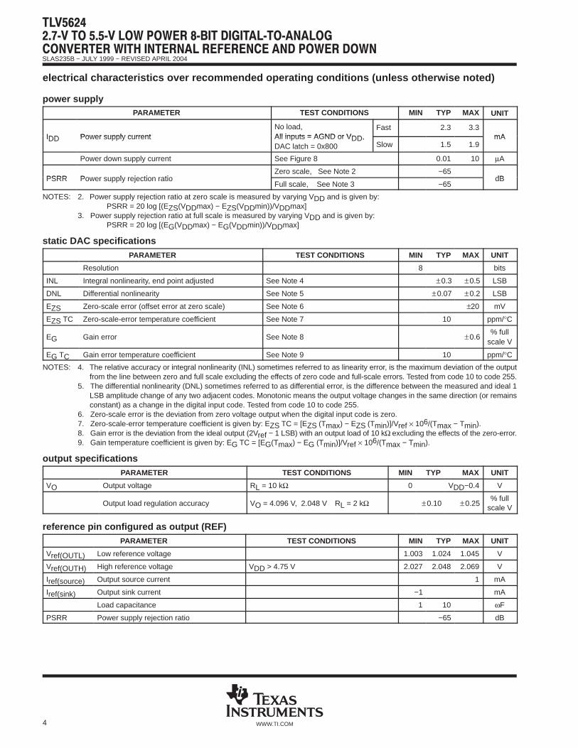
electrical characteristics over recommended operating conditions (unless otherwise noted)
power supplyPARAMETER TEST CONDITIONS MIN TYP MAX UNIT
IDD Power supply currentNo load,All inputs = AGND or VDD,
Fast 2.3 3.3mAIDD Power supply current All inputs = AGND or VDD,
DAC latch = 0x800 Slow 1.5 1.9mA
Power down supply current See Figure 8 0.01 10 µA
PSRR Power supply rejection ratioZero scale, See Note 2 −65
dBPSRR Power supply rejection ratioFull scale, See Note 3 −65
dB
NOTES: 2. Power supply rejection ratio at zero scale is measured by varying VDD and is given by:PSRR = 20 log [(EZS(VDDmax) − EZS(VDDmin))/VDDmax]
3. Power supply rejection ratio at full scale is measured by varying VDD and is given by:PSRR = 20 log [(EG(VDDmax) − EG(VDDmin))/VDDmax]
static DAC specificationsPARAMETER TEST CONDITIONS MIN TYP MAX UNIT
Resolution 8 bits
INL Integral nonlinearity, end point adjusted See Note 4 ±0.3 ±0.5 LSB
DNL Differential nonlinearity See Note 5 ±0.07 ±0.2 LSB
EZS Zero-scale error (offset error at zero scale) See Note 6 ±20 mV
EZS TC Zero-scale-error temperature coefficient See Note 7 10 ppm/°C
EG Gain error See Note 8 ±0.6% full
scale V
EG TC Gain error temperature coefficient See Note 9 10 ppm/°C
NOTES: 4. The relative accuracy or integral nonlinearity (INL) sometimes referred to as linearity error, is the maximum deviation of the outputfrom the line between zero and full scale excluding the effects of zero code and full-scale errors. Tested from code 10 to code 255.
5. The differential nonlinearity (DNL) sometimes referred to as differential error, is the difference between the measured and ideal 1LSB amplitude change of any two adjacent codes. Monotonic means the output voltage changes in the same direction (or remainsconstant) as a change in the digital input code. Tested from code 10 to code 255.
6. Zero-scale error is the deviation from zero voltage output when the digital input code is zero.7. Zero-scale-error temperature coefficient is given by: EZS TC = [EZS (Tmax) − EZS (Tmin)]/Vref × 106/(Tmax − Tmin).8. Gain error is the deviation from the ideal output (2Vref − 1 LSB) with an output load of 10 kΩ excluding the effects of the zero-error.9. Gain temperature coefficient is given by: EG TC = [EG(Tmax) − EG (Tmin)]/Vref × 106/(Tmax − Tmin).
output specificationsPARAMETER TEST CONDITIONS MIN TYP MAX UNIT
VO Output voltage RL = 10 kΩ 0 VDD−0.4 V
Output load regulation accuracy VO = 4.096 V, 2.048 V RL = 2 kΩ ±0.10 ±0.25% full
scale V
reference pin configured as output (REF)PARAMETER TEST CONDITIONS MIN TYP MAX UNIT
Vref(OUTL) Low reference voltage 1.003 1.024 1.045 V
Vref(OUTH) High reference voltage VDD > 4.75 V 2.027 2.048 2.069 V
Iref(source) Output source current 1 mA
Iref(sink) Output sink current −1 mA
Load capacitance 1 10 ωF
PSRR Power supply rejection ratio −65 dB

SLAS235B − JULY 1999 − REVISED APRIL 2004
5WWW.TI.COM
electrical characteristics over recommended operating conditions (unless otherwise noted)(Continued)
reference pin configured as input (REF)PARAMETER TEST CONDITIONS MIN TYP MAX UNIT
VI Input voltage 0 VDD−1.5 V
RI Input resistance 10 MΩ
CI Input capacitance 5 pF
Reference input bandwidth REF = 0.2 Vpp + 1.024 V dcFast 1.3 MHz
Reference input bandwidth REF = 0.2 Vpp + 1.024 V dcSlow 525 kHz
Reference feedthrough REF = 1 Vpp at 1 kHz + 1.024 V dc (see Note 10) −80 dB
NOTE 10: Reference feedthrough is measured at the DAC output with an input code = 0x000.
digital inputsPARAMETER TEST CONDITIONS MIN TYP MAX UNIT
IIH High-level digital input current VI = VDD 1 µA
IIL Low-level digital input current VI = 0 V −1 µA
Ci Input capacitance 8 pF
analog output dynamic performancePARAMETER TEST CONDITIONS MIN TYP MAX UNIT
ts(FS) Output settling time, full scaleRL = 10 kΩ, CL = 100 pF, Fast 1 3
sts(FS) Output settling time, full scaleRL = 10 kΩ, CL = 100 pF,See Note 11 Slow 3.5 7
µs
ts(CC) Output settling time, code to codeRL = 10 kΩ, CL = 100 pF, Fast 0.5 1.5
sts(CC) Output settling time, code to codeRL = 10 kΩ, CL = 100 pF,See Note 12 Slow 1 2
µs
SR Slew rateRL = 10 kΩ, CL = 100 pF, Fast 8
V/ sSR Slew rateRL = 10 kΩ, CL = 100 pF,See Note 13 Slow 1.5
V/µs
Glitch energyDIN = 0 to 1, fCLK = 100 kHz,CS = VDD
5 nV−S
SNR Signal-to-noise ratio 53 57
S/(N+D) Signal-to-noise + distortion fs = 480 kSPS, fout = 1 kHz, 48 47dB
THD Total harmonic distortion
fs = 480 kSPS, fout = 1 kHz,RL = 10 kΩ, CL = 100 pF −50 −48
dB
Spurious free dynamic range
RL = 10 k , CL = 100 pF
50 62
NOTES: 11. Settling time is the time for the output signal to remain within ±0.5 LSB of the final measured value for a digital input code changeof 0x020 to 0xFDFand 0xFDF to 0x020 respectively. Not tested, assured by design.
12. Settling time is the time for the output signal to remain within ± 0.5 LSB of the final measured value for a digital input code changeof one count. Not tested, assured by design.
13. Slew rate determines the time it takes for a change of the DAC output from 10% to 90% full-scale voltage.

SLAS235B − JULY 1999 − REVISED APRIL 2004
6 WWW.TI.COM
digital input timing requirements
MIN NOM MAX UNIT
tsu(CS−FS) Setup time, CS low before FS falling edge 10 ns
tsu(FS-CK) Setup time, FS low before first negative SCLK edge 8 ns
tsu(C16-FS)Setup time, 16th negative SCLK edge after FS low on which bit D0 is sampled before risingedge of FS
10 ns
tsu(C16-CS)
Setup time, 16th positive SCLK edge (first positive after D0 is sampled) before CS risingedge. If FS is used instead of 16th positive edge to update DAC, then setup time betweenFS rising edge and CS rising edge.
10 ns
twH SCLK pulse duration high 25 ns
twL SCLK pulse duration low 25 ns
tsu(D) Setup time, data ready before SCLK falling edge 8 ns
tH(D) Hold time, data held valid after SCLK falling edge 5 ns
twH(FS) FS pulse duration high 25 ns
PARAMETER MEASUREMENT INFORMATION
twL
SCLK
CS
DIN
FS
D15 D14 D13 D12 D1 D0 XX
1X 2 3 4 5 15 16 X
twH
tsu(D) th(D)
tsu(CS-FS)
twH(FS) tsu(FS-CK) tsu(C16-FS)
tsu(C16-CS)
Figure 1. Timing Diagram

SLAS235B − JULY 1999 − REVISED APRIL 2004
7WWW.TI.COM
TYPICAL CHARACTERISTICS
2.0685
2.0675
2.067
2.0660 0.5 1 1.5 2 2.5 3
Out
put V
olta
ge −
V
2.07
2.0705
Source Current − mA
OUTPUT VOLTAGEvs
LOAD CURRENT2.071
3.5 4
2.0695
2.0698
2.068
2.0665
Slow
Fast
VDD = 3 V, REF = Int. 1 V, Input Code = 255
Figure 2
VDD = 5 V, REF = Int. 2 V, Input Code = 255
4.132
4.131
4.13
4.1290 0.5 1 1.5 2 2.5 3
Out
put V
olta
ge −
V
4.133
4.134
Source Current − mA
OUTPUT VOLTAGEvs
LOAD CURRENT4.135
3.5 4
Slow
Fast
Figure 3
Figure 4
VDD = 3 V, REF = Int. 1 V,Input Code = 0
Slow
Fast
1.5
1
0.5
00 0.5 1 1.5 2 2.5 3
Out
put V
olta
ge −
V
2
2.5
Sink Current − mA
OUTPUT VOLTAGEvs
LOAD CURRENT3
3.5 4
VDD = 5 V, REF = Int. 2 V,Input Code = 0
Slow
Fast
3.5
2
1
00 0.5 1 1.5 2 2.5 3
Out
put V
olta
ge −
V
4
4.5
Sink Current − mA
OUTPUT VOLTAGEvs
LOAD CURRENT
5
3.5 4
3
2.5
1.5
0.5
Figure 5

SLAS235B − JULY 1999 − REVISED APRIL 2004
8 WWW.TI.COM
TYPICAL CHARACTERISTICS
Figure 6
1.5
1
0.5−40 −30 −20 −10 0 20 30
Sup
ply
Cur
rent
− m
A
2
2.5
SUPPLY CURRENTvs
TEMPERATURE3
40 50 70 9010 60 80
Fast Mode
Slow Mode
t − Temperature − °C
VDD = 5 V, REF = 2 V,Input Code = 255
Figure 7
1.5
1
0.5−40−30−20 −10 0 10 20
2
2.5
3
30 40 50 9060 70 80
Sup
ply
Cur
rent
− m
A
SUPPLY CURRENTvs
TEMPERATURE
Fast Mode
Slow Mode
t − Temperature − °C
VDD = 3 V, REF = 1 V,Input Code = 255
Figure 8
1.4
0.8
0.4
00 10 20 30 40
− P
ower
Dow
n S
uppl
y C
urre
nt −
mA
1.6
1.8
POWER DOWN SUPPLY CURRENTvs
TIME2
50 60 70 80
1.2
1
0.6
0.2
t − Time − µs
I DD
Figure 9
−40
−50
−80
−100100 1000
TH
D+N
− T
otal
Har
mon
ic D
isto
rtio
n an
d N
oise
− d
B
−20
−10
f − Frequency − Hz
TOTAL HARMONIC DISTORTION AND NOISEvs
FREQUENCY0
10000 100000
−30
−60
−70
−90
Fast Mode
Slow Mode
VDD = 5 VVref = 1 V dc + 1 V p/p SinewaveOutput Full Scale

SLAS235B − JULY 1999 − REVISED APRIL 2004
9WWW.TI.COM
TYPICAL CHARACTERISTICS
−40
−50
−80
−100100 1000
TH
D −
Tot
al H
arm
onic
Dis
tort
ion
− dB −20
−10
f − Frequency − Hz
TOTAL HARMONIC DISTORTIONvs
FREQUENCY0
10000 100000
−30
−60
−70
−90Fast Mode
Slow Mode
VDD = 5 VVref = 1 V dc + 1 V p/p SinewaveOutput Full Scale
Figure 10
Figure 11
−0.20
−0.15
−0.10
−0.05
−0.00
0.05
0.10
0.15
0.20
0 32 64 96 128 160 192 224 256DN
L −
Diff
eren
tial N
onlin
earit
y −
LSB
Digital Output Code
DIFFERENTIAL NONLINEARITYvs
DIGITAL OUTPUT CODE
SLAS235B − JULY 1999 − REVISED APRIL 2004
10 WWW.TI.COM
TYPICAL CHARACTERISTICS
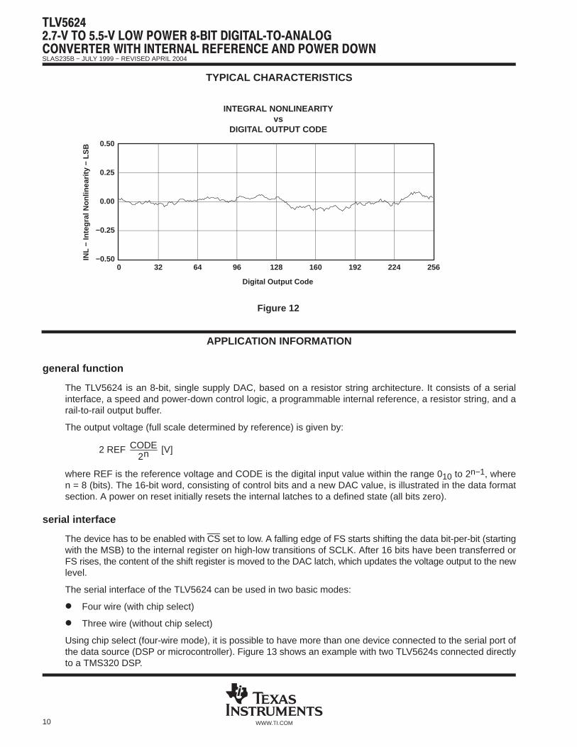
Figure 12
−0.50
−0.25
0.00
0.25
0.50
0 32 64 96 128 160 192 224 256
INL
− In
tegr
al N
onlin
earit
y −
LSB
Digital Output Code
INTEGRAL NONLINEARITYvs
DIGITAL OUTPUT CODE
APPLICATION INFORMATION
general function
The TLV5624 is an 8-bit, single supply DAC, based on a resistor string architecture. It consists of a serialinterface, a speed and power-down control logic, a programmable internal reference, a resistor string, and arail-to-rail output buffer.
The output voltage (full scale determined by reference) is given by:
2 REF CODE2n [V]
where REF is the reference voltage and CODE is the digital input value within the range 010 to 2n−1, wheren = 8 (bits). The 16-bit word, consisting of control bits and a new DAC value, is illustrated in the data formatsection. A power on reset initially resets the internal latches to a defined state (all bits zero).
serial interface
The device has to be enabled with CS set to low. A falling edge of FS starts shifting the data bit-per-bit (startingwith the MSB) to the internal register on high-low transitions of SCLK. After 16 bits have been transferred orFS rises, the content of the shift register is moved to the DAC latch, which updates the voltage output to the newlevel.
The serial interface of the TLV5624 can be used in two basic modes:
Four wire (with chip select)
Three wire (without chip select)
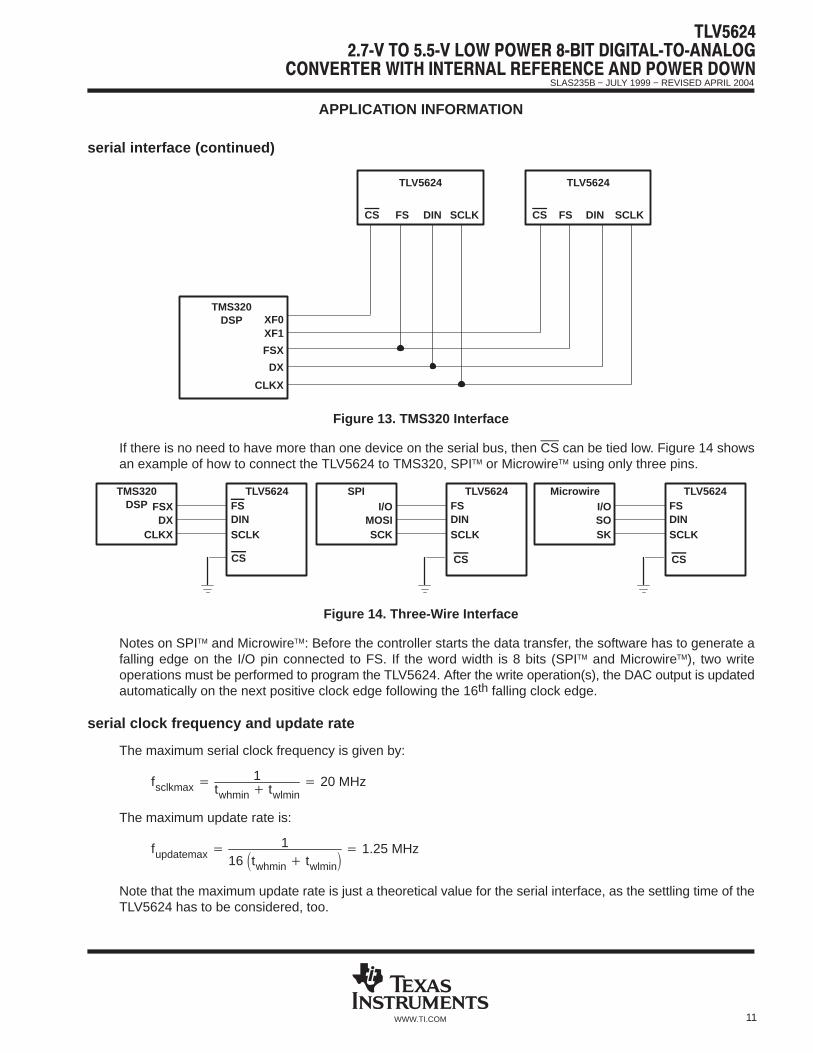
Using chip select (four-wire mode), it is possible to have more than one device connected to the serial port ofthe data source (DSP or microcontroller). Figure 13 shows an example with two TLV5624s connected directlyto a TMS320 DSP.
SLAS235B − JULY 1999 − REVISED APRIL 2004
11WWW.TI.COM
APPLICATION INFORMATION
serial interface (continued)
TMS320DSP XF0
CLKX
DX
FSX
XF1
TLV5624
CS FS DIN SCLK
TLV5624
CS FS DIN SCLK
Figure 13. TMS320 Interface
If there is no need to have more than one device on the serial bus, then CS can be tied low. Figure 14 showsan example of how to connect the TLV5624 to TMS320, SPI or Microwire using only three pins.
TMS320DSP FSX
CLKXDX
TLV5624
SCLKDINFS
SPII/O
SCKMOSI
TLV5624
SCLKDINFS
MicrowireI/O
SKSO
TLV5624
SCLKDINFS
CS CS CS
Figure 14. Three-Wire Interface
Notes on SPI and Microwire: Before the controller starts the data transfer, the software has to generate afalling edge on the I/O pin connected to FS. If the word width is 8 bits (SPI and Microwire), two writeoperations must be performed to program the TLV5624. After the write operation(s), the DAC output is updatedautomatically on the next positive clock edge following the 16th falling clock edge.
serial clock frequency and update rate
The maximum serial clock frequency is given by:
fsclkmax 1
twhmin twlmin 20 MHz
The maximum update rate is:
fupdatemax 1
16 twhmin twlmin 1.25 MHz
Note that the maximum update rate is just a theoretical value for the serial interface, as the settling time of theTLV5624 has to be considered, too.
SLAS235B − JULY 1999 − REVISED APRIL 2004
12 WWW.TI.COM
APPLICATION INFORMATION
data format
The 16-bit data word for the TLV5624 consists of two parts:
Program bits (D15..D12)
New data (D11..D0)
D15 D14 D13 D12 D11 D10 D9 D8 D7 D6 D5 D4 D3 D2 D1 D0
R1 SPD PWR R0 8 Data bits 0 0 0 0
SPD: Speed control bit 1 → fast mode 0 → slow modePWR: Power control bit 1 → power down 0 → normal operation
The following table lists the possible combination of the register select bits:
register select bitsR1 R0 REGISTER
0 0 Write data to DAC
0 1 Reserved
1 0 Reserved
1 1 Write data to control register
The meaning of the 12 data bits depends on the selected register. For the DAC register, bits D11...D4 determinethe new DAC output value:
data bits: DAC
D11 D10 D9 D8 D7 D6 D5 D4 D3 D2 D1 D0
New DAC Value 0 0 0 0
If the control register is selected, then D1, D0 of the 12 data bits are used to program the reference voltage:
data bits: CONTROL
D11 D10 D9 D8 D7 D6 D5 D4 D3 D2 D1 D0
X X X X X X X X X X REF1 REF2
X: don’t care
REF1 and REF0 determine the reference source and, if internal reference is selected, the reference voltage.
reference bitsREF1 REF0 REFERENCE
0 0 External
0 1 1.024 V
1 0 2.048 V
1 1 External
NOTE: A 0.1µF bypass capacitor must be installed onthe reference pin (pin 6). If internal reference is used a10 µF capacitor must also be installed for referencevoltage stability.
CAUTION:If external reference voltage is applied to the REF pin, external reference MUST be selected.
SLAS235B − JULY 1999 − REVISED APRIL 2004
13WWW.TI.COM
APPLICATION INFORMATION
Example:
Set DAC output, select fast mode, select internal reference at 2.048 V:
1. Set reference voltage to 2.048 V (CONTROL register):
D15 D14 D13 D12 D11 D10 D9 D8 D7 D6 D5 D4 D3 D2 D1 D0
1 1 0 1 0 0 0 0 0 0 0 0 0 0 1 0
2. Write new DAC value and update DAC output:
D15 D14 D13 D12 D11 D10 D9 D8 D7 D6 D5 D4 D3 D2 D1 D0
0 1 0 0 New DAC output value 0 0 0 0
The DAC output is updated on the rising clock edge after D0 is sampled.
To output data consecutively using the same DAC configuration, it is not necessary to program the CONTROLregister again.
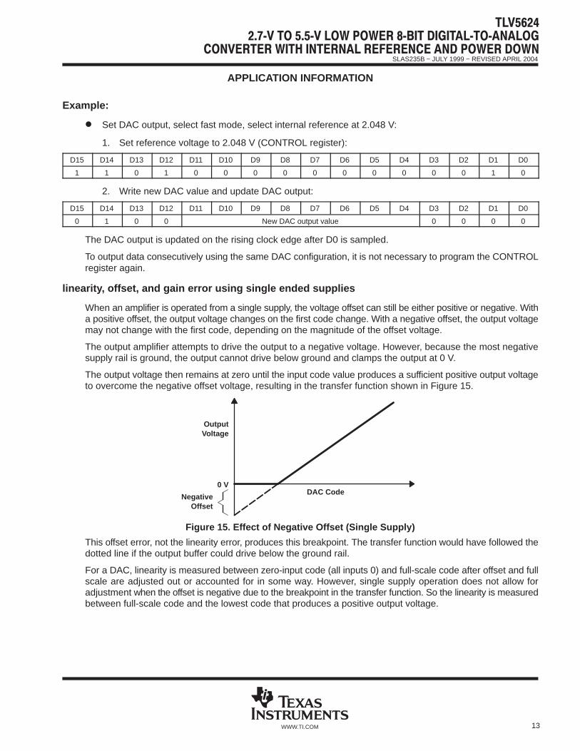
linearity, offset, and gain error using single ended supplies
When an amplifier is operated from a single supply, the voltage offset can still be either positive or negative. Witha positive offset, the output voltage changes on the first code change. With a negative offset, the output voltagemay not change with the first code, depending on the magnitude of the offset voltage.
The output amplifier attempts to drive the output to a negative voltage. However, because the most negativesupply rail is ground, the output cannot drive below ground and clamps the output at 0 V.
The output voltage then remains at zero until the input code value produces a sufficient positive output voltageto overcome the negative offset voltage, resulting in the transfer function shown in Figure 15.
DAC Code
OutputVoltage
0 V
NegativeOffset
Figure 15. Effect of Negative Offset (Single Supply)
This offset error, not the linearity error, produces this breakpoint. The transfer function would have followed thedotted line if the output buffer could drive below the ground rail.
For a DAC, linearity is measured between zero-input code (all inputs 0) and full-scale code after offset and fullscale are adjusted out or accounted for in some way. However, single supply operation does not allow foradjustment when the offset is negative due to the breakpoint in the transfer function. So the linearity is measuredbetween full-scale code and the lowest code that produces a positive output voltage.

SLAS235B − JULY 1999 − REVISED APRIL 2004
14 WWW.TI.COM
APPLICATION INFORMATION
power-supply bypassing and ground management
Printed-circuit boards that use separate analog and digital ground planes offer the best system performance.Wire-wrap boards do not perform well and should not be used. The two ground planes should be connectedtogether at the low-impedance power-supply source. The best ground connection may be achieved byconnecting the DAC AGND terminal to the system analog ground plane, making sure that analog groundcurrents are well managed and there are negligible voltage drops across the ground plane.
A 0.1-µF ceramic-capacitor bypass should be connected between VDD and AGND and mounted with short leadsas close as possible to the device. Use of ferrite beads may further isolate the system analog supply from thedigital power supply.
Figure 16 shows the ground plane layout and bypassing technique.
0.1 µF
Analog Ground Plane
1
2
3
4
8
7
6
5
Figure 16. Power-Supply Bypassing
definitions of specifications and terminology
integral nonlinearity (INL)
The relative accuracy or integral nonlinearity (INL), sometimes referred to as linearity error, is the maximumdeviation of the output from the line between zero and full scale excluding the effects of zero code and full-scaleerrors.
differential nonlinearity (DNL)
The differential nonlinearity (DNL), sometimes referred to as differential error, is the difference between themeasured and ideal 1 LSB amplitude change of any two adjacent codes. Monotonic means the output voltagechanges in the same direction (or remains constant) as a change in the digital input code.
zero-scale error (E ZS)
Zero-scale error is defined as the deviation of the output from 0 V at a digital input value of 0.
gain error (E G)
Gain error is the error in slope of the DAC transfer function.
total harmonic distortion (THD)
THD is the ratio of the rms value of the first six harmonic components to the value of the fundamental signal.The value for THD is expressed in decibels.
signal-to-noise ratio + distortion (S/N+D)
S/N+D is the ratio of the rms value of the output signal to the rms sum of all other spectral components belowthe Nyquist frequency, including harmonics but excluding dc. The value for S/N+D is expressed in decibels.
spurious free dynamic range (SFDR)
Spurious free dynamic range is the difference between the rms value of the output signal and the rms value ofthe largest spurious signal within a specified bandwidth. The value for SFDR is expressed in decibels.
PACKAGE OPTION ADDENDUM
www.ti.com 10-Jun-2014
Addendum-Page 1
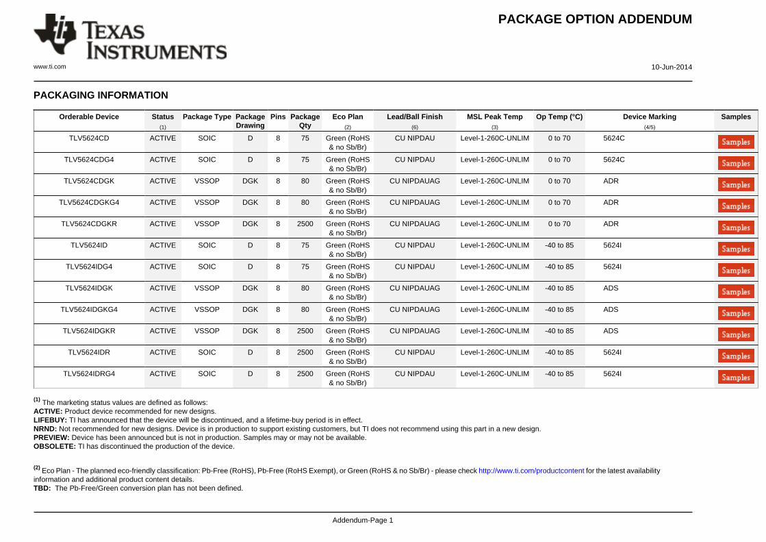
PACKAGING INFORMATION
Orderable Device Status(1)
Package Type PackageDrawing
Pins PackageQty
Eco Plan(2)
Lead/Ball Finish(6)
MSL Peak Temp(3)
Op Temp (°C) Device Marking(4/5)
Samples
TLV5624CD ACTIVE SOIC D 8 75 Green (RoHS& no Sb/Br)
CU NIPDAU Level-1-260C-UNLIM 0 to 70 5624C
TLV5624CDG4 ACTIVE SOIC D 8 75 Green (RoHS& no Sb/Br)
CU NIPDAU Level-1-260C-UNLIM 0 to 70 5624C
TLV5624CDGK ACTIVE VSSOP DGK 8 80 Green (RoHS& no Sb/Br)
CU NIPDAUAG Level-1-260C-UNLIM 0 to 70 ADR
TLV5624CDGKG4 ACTIVE VSSOP DGK 8 80 Green (RoHS& no Sb/Br)
CU NIPDAUAG Level-1-260C-UNLIM 0 to 70 ADR
TLV5624CDGKR ACTIVE VSSOP DGK 8 2500 Green (RoHS& no Sb/Br)
CU NIPDAUAG Level-1-260C-UNLIM 0 to 70 ADR
TLV5624ID ACTIVE SOIC D 8 75 Green (RoHS& no Sb/Br)
CU NIPDAU Level-1-260C-UNLIM -40 to 85 5624I
TLV5624IDG4 ACTIVE SOIC D 8 75 Green (RoHS& no Sb/Br)
CU NIPDAU Level-1-260C-UNLIM -40 to 85 5624I
TLV5624IDGK ACTIVE VSSOP DGK 8 80 Green (RoHS& no Sb/Br)
CU NIPDAUAG Level-1-260C-UNLIM -40 to 85 ADS
TLV5624IDGKG4 ACTIVE VSSOP DGK 8 80 Green (RoHS& no Sb/Br)
CU NIPDAUAG Level-1-260C-UNLIM -40 to 85 ADS
TLV5624IDGKR ACTIVE VSSOP DGK 8 2500 Green (RoHS& no Sb/Br)
CU NIPDAUAG Level-1-260C-UNLIM -40 to 85 ADS
TLV5624IDR ACTIVE SOIC D 8 2500 Green (RoHS& no Sb/Br)
CU NIPDAU Level-1-260C-UNLIM -40 to 85 5624I
TLV5624IDRG4 ACTIVE SOIC D 8 2500 Green (RoHS& no Sb/Br)
CU NIPDAU Level-1-260C-UNLIM -40 to 85 5624I
(1) The marketing status values are defined as follows:ACTIVE: Product device recommended for new designs.LIFEBUY: TI has announced that the device will be discontinued, and a lifetime-buy period is in effect.NRND: Not recommended for new designs. Device is in production to support existing customers, but TI does not recommend using this part in a new design.PREVIEW: Device has been announced but is not in production. Samples may or may not be available.OBSOLETE: TI has discontinued the production of the device.
(2) Eco Plan - The planned eco-friendly classification: Pb-Free (RoHS), Pb-Free (RoHS Exempt), or Green (RoHS & no Sb/Br) - please check http://www.ti.com/productcontent for the latest availabilityinformation and additional product content details.TBD: The Pb-Free/Green conversion plan has not been defined.
PACKAGE OPTION ADDENDUM
www.ti.com 10-Jun-2014
Addendum-Page 2
Pb-Free (RoHS): TI's terms "Lead-Free" or "Pb-Free" mean semiconductor products that are compatible with the current RoHS requirements for all 6 substances, including the requirement thatlead not exceed 0.1% by weight in homogeneous materials. Where designed to be soldered at high temperatures, TI Pb-Free products are suitable for use in specified lead-free processes.Pb-Free (RoHS Exempt): This component has a RoHS exemption for either 1) lead-based flip-chip solder bumps used between the die and package, or 2) lead-based die adhesive used betweenthe die and leadframe. The component is otherwise considered Pb-Free (RoHS compatible) as defined above.Green (RoHS & no Sb/Br): TI defines "Green" to mean Pb-Free (RoHS compatible), and free of Bromine (Br) and Antimony (Sb) based flame retardants (Br or Sb do not exceed 0.1% by weightin homogeneous material)
(3) MSL, Peak Temp. - The Moisture Sensitivity Level rating according to the JEDEC industry standard classifications, and peak solder temperature.
(4) There may be additional marking, which relates to the logo, the lot trace code information, or the environmental category on the device.
(5) Multiple Device Markings will be inside parentheses. Only one Device Marking contained in parentheses and separated by a "~" will appear on a device. If a line is indented then it is a continuationof the previous line and the two combined represent the entire Device Marking for that device.
(6) Lead/Ball Finish - Orderable Devices may have multiple material finish options. Finish options are separated by a vertical ruled line. Lead/Ball Finish values may wrap to two lines if the finishvalue exceeds the maximum column width.
Important Information and Disclaimer:The information provided on this page represents TI's knowledge and belief as of the date that it is provided. TI bases its knowledge and belief on informationprovided by third parties, and makes no representation or warranty as to the accuracy of such information. Efforts are underway to better integrate information from third parties. TI has taken andcontinues to take reasonable steps to provide representative and accurate information but may not have conducted destructive testing or chemical analysis on incoming materials and chemicals.TI and TI suppliers consider certain information to be proprietary, and thus CAS numbers and other limited information may not be available for release.
In no event shall TI's liability arising out of such information exceed the total purchase price of the TI part(s) at issue in this document sold by TI to Customer on an annual basis.
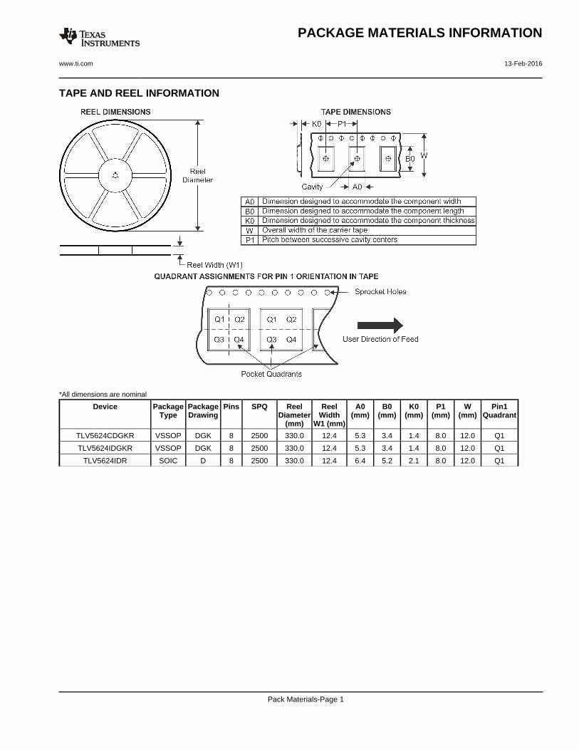
TAPE AND REEL INFORMATION
*All dimensions are nominal
Device PackageType
PackageDrawing
Pins SPQ ReelDiameter
(mm)
ReelWidth
W1 (mm)
A0(mm)
B0(mm)
K0(mm)
P1(mm)
W(mm)
Pin1Quadrant
TLV5624CDGKR VSSOP DGK 8 2500 330.0 12.4 5.3 3.4 1.4 8.0 12.0 Q1
TLV5624IDGKR VSSOP DGK 8 2500 330.0 12.4 5.3 3.4 1.4 8.0 12.0 Q1
TLV5624IDR SOIC D 8 2500 330.0 12.4 6.4 5.2 2.1 8.0 12.0 Q1
PACKAGE MATERIALS INFORMATION
www.ti.com 13-Feb-2016
Pack Materials-Page 1
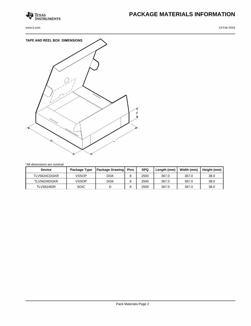
*All dimensions are nominal
Device Package Type Package Drawing Pins SPQ Length (mm) Width (mm) Height (mm)
TLV5624CDGKR VSSOP DGK 8 2500 367.0 367.0 38.0
TLV5624IDGKR VSSOP DGK 8 2500 367.0 367.0 38.0
TLV5624IDR SOIC D 8 2500 367.0 367.0 38.0
PACKAGE MATERIALS INFORMATION
www.ti.com 13-Feb-2016
Pack Materials-Page 2


IMPORTANT NOTICE
Texas Instruments Incorporated and its subsidiaries (TI) reserve the right to make corrections, enhancements, improvements and otherchanges to its semiconductor products and services per JESD46, latest issue, and to discontinue any product or service per JESD48, latestissue. Buyers should obtain the latest relevant information before placing orders and should verify that such information is current andcomplete. All semiconductor products (also referred to herein as “components”) are sold subject to TI’s terms and conditions of salesupplied at the time of order acknowledgment.TI warrants performance of its components to the specifications applicable at the time of sale, in accordance with the warranty in TI’s termsand conditions of sale of semiconductor products. Testing and other quality control techniques are used to the extent TI deems necessaryto support this warranty. Except where mandated by applicable law, testing of all parameters of each component is not necessarilyperformed.TI assumes no liability for applications assistance or the design of Buyers’ products. Buyers are responsible for their products andapplications using TI components. To minimize the risks associated with Buyers’ products and applications, Buyers should provideadequate design and operating safeguards.TI does not warrant or represent that any license, either express or implied, is granted under any patent right, copyright, mask work right, orother intellectual property right relating to any combination, machine, or process in which TI components or services are used. Informationpublished by TI regarding third-party products or services does not constitute a license to use such products or services or a warranty orendorsement thereof. Use of such information may require a license from a third party under the patents or other intellectual property of thethird party, or a license from TI under the patents or other intellectual property of TI.Reproduction of significant portions of TI information in TI data books or data sheets is permissible only if reproduction is without alterationand is accompanied by all associated warranties, conditions, limitations, and notices. TI is not responsible or liable for such altereddocumentation. Information of third parties may be subject to additional restrictions.Resale of TI components or services with statements different from or beyond the parameters stated by TI for that component or servicevoids all express and any implied warranties for the associated TI component or service and is an unfair and deceptive business practice.TI is not responsible or liable for any such statements.Buyer acknowledges and agrees that it is solely responsible for compliance with all legal, regulatory and safety-related requirementsconcerning its products, and any use of TI components in its applications, notwithstanding any applications-related information or supportthat may be provided by TI. Buyer represents and agrees that it has all the necessary expertise to create and implement safeguards whichanticipate dangerous consequences of failures, monitor failures and their consequences, lessen the likelihood of failures that might causeharm and take appropriate remedial actions. Buyer will fully indemnify TI and its representatives against any damages arising out of the useof any TI components in safety-critical applications.In some cases, TI components may be promoted specifically to facilitate safety-related applications. With such components, TI’s goal is tohelp enable customers to design and create their own end-product solutions that meet applicable functional safety standards andrequirements. Nonetheless, such components are subject to these terms.No TI components are authorized for use in FDA Class III (or similar life-critical medical equipment) unless authorized officers of the partieshave executed a special agreement specifically governing such use.Only those TI components which TI has specifically designated as military grade or “enhanced plastic” are designed and intended for use inmilitary/aerospace applications or environments. Buyer acknowledges and agrees that any military or aerospace use of TI componentswhich have not been so designated is solely at the Buyer's risk, and that Buyer is solely responsible for compliance with all legal andregulatory requirements in connection with such use.TI has specifically designated certain components as meeting ISO/TS16949 requirements, mainly for automotive use. In any case of use ofnon-designated products, TI will not be responsible for any failure to meet ISO/TS16949.
Products ApplicationsAudio www.ti.com/audio Automotive and Transportation www.ti.com/automotiveAmplifiers amplifier.ti.com Communications and Telecom www.ti.com/communicationsData Converters dataconverter.ti.com Computers and Peripherals www.ti.com/computersDLP® Products www.dlp.com Consumer Electronics www.ti.com/consumer-appsDSP dsp.ti.com Energy and Lighting www.ti.com/energyClocks and Timers www.ti.com/clocks Industrial www.ti.com/industrialInterface interface.ti.com Medical www.ti.com/medicalLogic logic.ti.com Security www.ti.com/securityPower Mgmt power.ti.com Space, Avionics and Defense www.ti.com/space-avionics-defenseMicrocontrollers microcontroller.ti.com Video and Imaging www.ti.com/videoRFID www.ti-rfid.comOMAP Applications Processors www.ti.com/omap TI E2E Community e2e.ti.comWireless Connectivity www.ti.com/wirelessconnectivity
Mailing Address: Texas Instruments, Post Office Box 655303, Dallas, Texas 75265Copyright © 2016, Texas Instruments Incorporated