LM25007 42V, 0.5A Step-DownSwitching Regulator
22
LM25007 www.ti.com SNVS401C – JANUARY 2006 – REVISED FEBRUARY 2013 LM25007 42V, 0.5A Step-Down Switching Regulator Check for Samples: LM25007 1FEATURES DESCRIPTION The LM25007 is a monolithic step-down switching 2• Integrated 0.74Ω N-Channel MOSFET Switch regulator featuring all of the functions needed to • Guaranteed 0.5A Output Current implement a low cost, efficient, power supply. • Ultra-Fast Transient Response Capable of driving a 0.5A load over a 9V-42V input voltage range, this device is easy to apply and is • Up to 800kHz Operation provided in the small VSSOP-8 and the thermally • No Control Loop Compensation Required enhanced WSON-8 packages. Ultra-fast transient • Vin Feed Forward Provides Constant response is achieved through the use of a constant Operating Frequency on-time architecture with Vin feed forward. This feature provides an almost constant operating • 2% Accurate 2.5V Feedback from -40°C to frequency over load and input voltage variations. The 125°C operating frequency can be adjusted with a single • Highly Efficient Operation resistor. This architecture is easy to use and tolerant • Intelligent Current Limit Protection of component selection. An intelligent current limit is implemented in the LM25007 with forced off time that • External Shutdown Control is inversely proportional to Vout thus ensuring • Thermal Shutdown recovery from fault conditions. The output voltage • VSSOP and Thermally Enhanced WSON may be set from 2.5V to >30V. To improve efficiency Packages in light load applications, the Vcc pin can be connected to an external voltage source to eliminate the drop through the internal regulator. Additional TYPICAL APPLICATIONS features include: thermal shutdown, Vcc under- • 12VDC and 24VDC Distributed Rail Systems voltage lockout, gate drive under-voltage lockout, and • 24VAC Systems max duty cycle limiter. • Automotive Body Electronics and Telematics • Industrial Systems • HB-LED Constant Current Source • Package: – VSSOP-8 – WSON-8 (4mm x 4mm) 1 Please be aware that an important notice concerning availability, standard warranty, and use in critical applications of Texas Instruments semiconductor products and disclaimers thereto appears at the end of this data sheet. 2All trademarks are the property of their respective owners. PRODUCTION DATA information is current as of publication date. Copyright © 2006–2013, Texas Instruments Incorporated Products conform to specifications per the terms of the Texas Instruments standard warranty. Production processing does not necessarily include testing of all parameters.
Transcript of LM25007 42V, 0.5A Step-DownSwitching Regulator

LM25007
www.ti.com SNVS401C –JANUARY 2006–REVISED FEBRUARY 2013
LM25007 42V, 0.5A Step-Down Switching RegulatorCheck for Samples: LM25007
1FEATURES DESCRIPTIONThe LM25007 is a monolithic step-down switching
2• Integrated 0.74Ω N-Channel MOSFET Switchregulator featuring all of the functions needed to
• Guaranteed 0.5A Output Current implement a low cost, efficient, power supply.• Ultra-Fast Transient Response Capable of driving a 0.5A load over a 9V-42V input
voltage range, this device is easy to apply and is• Up to 800kHz Operationprovided in the small VSSOP-8 and the thermally• No Control Loop Compensation Required enhanced WSON-8 packages. Ultra-fast transient
• Vin Feed Forward Provides Constant response is achieved through the use of a constantOperating Frequency on-time architecture with Vin feed forward. This
feature provides an almost constant operating• 2% Accurate 2.5V Feedback from -40°C tofrequency over load and input voltage variations. The125°Coperating frequency can be adjusted with a single
• Highly Efficient Operation resistor. This architecture is easy to use and tolerant• Intelligent Current Limit Protection of component selection. An intelligent current limit is
implemented in the LM25007 with forced off time that• External Shutdown Controlis inversely proportional to Vout thus ensuring• Thermal Shutdown recovery from fault conditions. The output voltage
• VSSOP and Thermally Enhanced WSON may be set from 2.5V to >30V. To improve efficiencyPackages in light load applications, the Vcc pin can be
connected to an external voltage source to eliminatethe drop through the internal regulator. AdditionalTYPICAL APPLICATIONSfeatures include: thermal shutdown, Vcc under-
• 12VDC and 24VDC Distributed Rail Systems voltage lockout, gate drive under-voltage lockout, and• 24VAC Systems max duty cycle limiter.• Automotive Body Electronics and Telematics• Industrial Systems• HB-LED Constant Current Source• Package:
– VSSOP-8– WSON-8 (4mm x 4mm)
1
Please be aware that an important notice concerning availability, standard warranty, and use in critical applications ofTexas Instruments semiconductor products and disclaimers thereto appears at the end of this data sheet.
2All trademarks are the property of their respective owners.
PRODUCTION DATA information is current as of publication date. Copyright © 2006–2013, Texas Instruments IncorporatedProducts conform to specifications per the terms of the TexasInstruments standard warranty. Production processing does notnecessarily include testing of all parameters.

1
2
3
4 5
6
7
8SW
BST
RCL
FBRTN
RON
VCC
VIN
FB
VIN
SW
RTN
BST
L1
C2
R3
R4
C4
C3
Input
LM25007
D1R5
8
6
5
3
4
1
2
7
SHUTDOWN
GND
RCL
VCC
C5
GND
9V ± 42V
RON/SD
RCL
RON
VOUT
C1
LM25007
SNVS401C –JANUARY 2006–REVISED FEBRUARY 2013 www.ti.com
Basic Step-Down Regulator
Connection Diagram
8-Lead VSSOP, WSON
2 Submit Documentation Feedback Copyright © 2006–2013, Texas Instruments Incorporated
Product Folder Links: LM25007

FB
VIN
VCC
SW
RTN
ON TIMER
DRIVER
VIN
BST
LEVELSHIFT
SD/RON
2.5V
THERMALSHUTDOWN
0.725A
BUCKSWITCH
CURRENTSENSE
COMPLETE
RCLSTARTRCL
COMPLETE
START
Ron
100 PHL1
C215 PF
R33.01k
R41k
R2100k
RON
200k
C40.01 PF
C30.1 PF
12V -42V
10V
LM25007
UVLO
FB R51
UVLO
REGULATIONCOMPARATOR
OVER-VOLTAGECOMPARATOR
2.875V
SD
SD
COMPLETE
START
MINIMUM OFF TIMER
C11 PF
8
6
5
3
4
1
2
7
7V SERIESREGULATOR
CURRENT LIMITOFF TIMER
SHUTDOWN
C50.1 PF, 100V
D1
QCLR
QSET
S
R
+-
+-
+-
LM25007
www.ti.com SNVS401C –JANUARY 2006–REVISED FEBRUARY 2013
Pin DescriptionsPin Name Description Application Information
1 SW Switching Node Power switching node. Connect to the inductor, bootstrap capacitor, and free-wheelingdiode.
2 BST Boost Boot–strap An external capacitor is required between the BST and the SW pins. A 0.01µF ceramiccapacitor input capacitor is recommended.
3 RCL Current Limit OFF time A resistor between this pin and RTN sets the off-time when current limit is detected.programming pin The off-time is preset to 17 µs if FB = 0V .
4 RTN Circuit Ground
5 FB Feedback Signal from This pin is connected to the inverting input of the internal regulation comparator. TheRegulated Output regulation threshold is 2.5V.
6 RON/SD On-time set pin A resistor between this pin and VIN sets the switch on-time as a function of Vin. Theminimum recommended on-time is 300ns at the maximum input voltage.
7 VCC Output from the internal If an auxiliary voltage is available to raise the voltage on this pin above the regulationhigh voltage bias setpoint (7V), the internal series pass regulator will shutdown, reducing the IC powerregulator. dissipation. Do not exceed 14V. This output provides gate drive power for the internal
Buck switch. An internal diode is provided between this pin and the BST pin. A local0.1uF decoupling capacitor is recommended.
8 VIN Input supply voltage Recommended operating range: 9V to 42V.
- EP Exposed pad, underside Exposed metal pad on the WSON package underside. It is recommended to connectof the WSON package this pad to the PC board ground plane to aid in heat dissipation.option
Typical Application Circuit and Block Diagram
Copyright © 2006–2013, Texas Instruments Incorporated Submit Documentation Feedback 3
Product Folder Links: LM25007

LM25007
SNVS401C –JANUARY 2006–REVISED FEBRUARY 2013 www.ti.com
These devices have limited built-in ESD protection. The leads should be shorted together or the device placed in conductive foamduring storage or handling to prevent electrostatic damage to the MOS gates.
Absolute Maximum Ratings (1)
VIN to RTN 45V
BST to RTN 59V
SW to RTN (Steady State) -1V
ESD Rating, Human Body Model (2) 2kV
BST to VCC 45V
BST to SW 14V
VCC to RTN 14V
All Other Inputs to RTN -0.3 to 7V
Storage Temperature Range -65°C to +150°C
(1) Absolute Maximum Ratings are limits beyond which damage to the device may occur. Operating Ratings are conditions under whichoperation of the device is intended to be functional. For guaranteed specifications and test conditions, see the Electrical Characteristics.
(2) The human body model is a 100pF capacitor discharge through a 1.5kΩ resistor into each pin. The human body ESD compliance levelfor Pin 7 and 8 is 1000V.
Operating Ratings (1)
VIN 9V to 42V
Junction Temperature −40°C to + 125°C
(1) Absolute Maximum Ratings are limits beyond which damage to the device may occur. Operating Ratings are conditions under whichoperation of the device is intended to be functional. For guaranteed specifications and test conditions, see the Electrical Characteristics.
4 Submit Documentation Feedback Copyright © 2006–2013, Texas Instruments Incorporated
Product Folder Links: LM25007
LM25007
www.ti.com SNVS401C –JANUARY 2006–REVISED FEBRUARY 2013
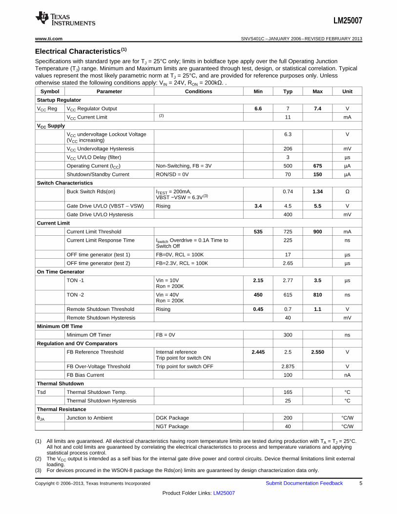
Electrical Characteristics (1)
Specifications with standard type are for TJ = 25°C only; limits in boldface type apply over the full Operating JunctionTemperature (TJ) range. Minimum and Maximum limits are guaranteed through test, design, or statistical correlation. Typicalvalues represent the most likely parametric norm at TJ = 25°C, and are provided for reference purposes only. Unlessotherwise stated the following conditions apply: VIN = 24V, RON = 200kΩ. .
Symbol Parameter Conditions Min Typ Max Unit
Startup Regulator
VCC Reg VCC Regulator Output 6.6 7 7.4 V
VCC Current Limit (2) 11 mA
VCC Supply
VCC undervoltage Lockout Voltage 6.3 V(VCC increasing)
VCC Undervoltage Hysteresis 206 mV
VCC UVLO Delay (filter) 3 µs
Operating Current (ICC) Non-Switching, FB = 3V 500 675 µA
Shutdown/Standby Current RON/SD = 0V 70 150 µA
Switch Characteristics
Buck Switch Rds(on) ITEST = 200mA, 0.74 1.34 ΩVBST −VSW = 6.3V (3)
Gate Drive UVLO (VBST – VSW) Rising 3.4 4.5 5.5 V
Gate Drive UVLO Hysteresis 400 mV
Current Limit
Current Limit Threshold 535 725 900 mA
Current Limit Response Time Iswitch Overdrive = 0.1A Time to 225 nsSwitch Off
OFF time generator (test 1) FB=0V, RCL = 100K 17 µs
OFF time generator (test 2) FB=2.3V, RCL = 100K 2.65 µs
On Time Generator
TON -1 Vin = 10V 2.15 2.77 3.5 µsRon = 200K
TON -2 Vin = 40V 450 615 810 nsRon = 200K
Remote Shutdown Threshold Rising 0.45 0.7 1.1 V
Remote Shutdown Hysteresis 40 mV
Minimum Off Time
Minimum Off Timer FB = 0V 300 ns
Regulation and OV Comparators
FB Reference Threshold Internal reference 2.445 2.5 2.550 VTrip point for switch ON
FB Over-Voltage Threshold Trip point for switch OFF 2.875 V
FB Bias Current 100 nA
Thermal Shutdown
Tsd Thermal Shutdown Temp. 165 °C
Thermal Shutdown Hysteresis 25 °C
Thermal Resistance
θJA Junction to Ambient DGK Package 200 °C/W
NGT Package 40 °C/W
(1) All limits are guaranteed. All electrical characteristics having room temperature limits are tested during production with TA = TJ = 25°C.All hot and cold limits are guaranteed by correlating the electrical characteristics to process and temperature variations and applyingstatistical process control.
(2) The VCC output is intended as a self bias for the internal gate drive power and control circuits. Device thermal limitations limit externalloading.
(3) For devices procured in the WSON-8 package the Rds(on) limits are guaranteed by design characterization data only.
Copyright © 2006–2013, Texas Instruments Incorporated Submit Documentation Feedback 5
Product Folder Links: LM25007

ON
-TIM
E (
ns)
100
1000
10000
0 20
INPUT VOLTAGE VIN (V)
423010
RON = 300k
200k
100k
0 0.5 1 1.5 2 2.50
2
4
6
8
10
12
14
16
18
20
VFB (V)
TO
FF
(P
s)
600k
400k200k
100k 50k
0 100 200 300 400 50070
80
90
100
EF
FIC
IEN
CY
(%
)
LOAD CURRENT (mA)
VIN = 15V
30V
42V
LM25007
SNVS401C –JANUARY 2006–REVISED FEBRUARY 2013 www.ti.com
Typical Performance Characteristics
Operational Waveforms Operational Waveforms
LM25007 Operation: VOUT = 10V, VIN = 20V, IOUT = 250mALM25007 Operation: VOUT = 10V, VIN = 42V, IOUT = 250mA
CH1: Switch Node, CH2: VOUT (AC), CH4: Inductor CurrentCH1: Switch Node, CH2: VOUT (AC), CH4: Inductor Current
Figure 1. Figure 2.
Current Limit Off-TimeLM25007 10V Output Efficiency vs VFB
Figure 3. Figure 4.
VINvs TON
RON = 100k, 200k, 300k
Figure 5.
6 Submit Documentation Feedback Copyright © 2006–2013, Texas Instruments Incorporated
Product Folder Links: LM25007

F =
VOUT
1.42 x 10⁻¹⁰ x RON
F =
VOUT2 x L
1 x 10-20 x RLoad x (RON)2
LM25007
www.ti.com SNVS401C –JANUARY 2006–REVISED FEBRUARY 2013
DETAILED OPERATING DESCRIPTION
The LM25007 is a monolithic step-down switching regulator featuring all of the functions needed to implementlow cost, efficient, power supply. Capable of driving a 0.5Amp load over a 9-42V input voltage range, this deviceis easy to apply and is provided in the small VSSOP-8 and the thermally enhanced WSON-8 packages. Ultra-fasttransient response is achieved through the use of a constant on-time architecture with Vin feed forward. Thisfeature provides and almost constant operating frequency over load and input voltage variations. The operatingfrequency may be adjusted up to 800kHz depending on input and output voltages. This architecture is easy touse and tolerant of component selection. An intelligent current limit is implemented in the LM25007 with forcedoff time that is inversely proportional to Vout to ensure recovery from fault conditions. The output voltage may beset from 2.5V to >30V. To improve efficiency in light load applications, the Vcc pin can be tied to an externalvoltage source thus eliminating the drop through the integrated internal regulator. Additional protection featuresinclude: thermal shutdown, Vcc under-voltage lockout, gate drive under-voltage lockout, and max duty cyclelimiter.
Hysteretic Control Circuit Overview
The LM25007 is a Buck DC-DC regulator that uses a constant on-time control scheme. The on-time isprogrammed by an external resistor and varies inversely with line input voltage (Vin). The core regulationelements of the LM25007 are the feedback comparator and the on-time one-shot. The regulator output voltage issensed at the feedback pin (FB) and is compared to an internal reference voltage (2.5V). If the FB signal isbelow the reference voltage, the buck switch is turned on for a fixed time pulse determined by the line voltageand a programming resistor (RON). Following the on period the switch will remain off for at least the minimum offtimer period of 300ns. If the FB pin voltage is still below the reference after the 300ns off-time, the switch will turnon again for another on time period. This switching behavior will continue until the FB pin voltage reaches thereference voltage level.
The LM25007 operates in discontinuous conduction mode at light load currents or continuous conduction modeat heavier load currents. In discontinuous conduction mode, current through the output inductor starts at zero andramps up to a peak value during the buck switch on-time and then back to zero during the off-time. The inductorcurrent remains at zero until the next on-time period starts when FB falls below the internal reference. Indiscontinuous mode the operating frequency is relatively low and will vary with load. Therefore at light loads theconversion efficiency is maintained, since the switching losses decrease with the reduction in load current andswitching frequency. The approximate discontinuous mode operating frequency can be calculated as follows:
(1)
In continuous conduction mode, current flows continuously through the inductor and never ramps down to zero.In this mode the operating frequency is greater than the discontinuous mode frequency and remains relativelyconstant with load and line variations. The approximate continuous mode operating frequency can be calculatedas follows:
(2)
The output voltage (Vout) can be programmed by two external resistors as shown in Figure 6. The regulatedvoltage is calculated as follows:
VOUT = 2.5 x (R3 + R4) / R4 (3)
The feedback comparator in hysteretic regulators depends on the output ripple voltage to switch the outputtransistor on and off at regular intervals. In order for the internal comparator to respond quickly to changes inoutput voltage, proportional to inductor current, a minimum amount of capacitor Equivalent Series Resistance(ESR) is required. A ripple voltage of 25mV is recommended at the feedback pin (FB) for stable operation. Incases where the intrinsic capacitor ESR is too small, additional series resistance may be added.
Copyright © 2006–2013, Texas Instruments Incorporated Submit Documentation Feedback 7
Product Folder Links: LM25007

+-
+
FB
REF2.5V
SWL
R3
R4
R5
VIN
LM25007
COUT
VOUT
LM25007
SNVS401C –JANUARY 2006–REVISED FEBRUARY 2013 www.ti.com
For applications where lower output voltage ripple is required the load can be connected directly to the low ESRoutput capacitor, as shown in Figure 6. The series resistor (R5) will degrade the load regulation. Anothertechnique for enhancing the ripple voltage at the FB pin is to place a capacitor in parallel with the feedbackdivider resistor R3. The addition of the capacitor reduces the attenuation of the ripple voltage from the feedbackdivider.
High Voltage Bias Regulator (VCC)
The LM25007 contains an internal high voltage bias regulator. The input pin (Vin) can be connected directly toline voltages from 9 to 42 Volts. To avoid supply voltage transients due to long lead inductances on the input pin(VIN), it is always recommended to connect a low ESR ceramic chip capacitor (≊ 0.1µF) between VIN and RTNpins located close to the LM25007. The regulator is internally current limited to 11mA. Upon power up, theregulator is enabled and sources current into an external capacitor connected to the VCC pin. When the voltageon the VCC pin reaches its UVLO level (6.3V), the controller output is enabled.
An external auxiliary supply voltage can be diode connected to the Vcc pin. If the auxiliary voltage is greater than7 Volts the internal regulator will shutoff, thus reducing internal power dissipation. Do not exceed 14V at VCC.See Figure 7.
Figure 6. Low Ripple Output Configuration
8 Submit Documentation Feedback Copyright © 2006–2013, Texas Instruments Incorporated
Product Folder Links: LM25007

+
+
+
7V SERIES REGULATOR
SWLM25007
VIN
BST
VCC
SELF-BIASDIODE
0.01 PF
0.1 PF
10V
10k
30k
LM25007
www.ti.com SNVS401C –JANUARY 2006–REVISED FEBRUARY 2013
Figure 7. Self Biased Configuration
Over-Voltage Comparator
The over-voltage comparator is provided to protect the output from overvoltage conditions due to sudden inputline voltage changes or output loading changes. The over-voltage comparator monitors the FB pin versus aninternal 2.875V reference. If the voltage at FB rises above 2.875V the comparator immediately terminates thebuck switch on-time pulse.
ON Time generator and Shutdown
The on-time of the LM25007 is set inversely proportional to the input voltage by an external resistor connectedbetween RON/SD and VIN. The RON/SD terminal is a low impedance input biased at approximately 1.5V. Thecurrent through the resistor and into the RON/SD pin is approximately proportional to Vin and used internally tocontrol the on-timer. This scheme of input voltage feed-forward hysteretic operation achieves nearly constantoperational frequency over varying line and load conditions. The on-time equation for the LM25007 is :
Ton = 1.42 x 10⁻¹⁰ x RON / VIN (4)
The RON/SD pin of the LM25007 also provides a shutdown function which disables the regulator andsignificantly decreases quiescent power dissipation. By pulling the pin below 0.7V activates the low powershutdown mode. The VIN quiescent current in the shutdown mode is approximately 100µA internal to theLM25007 plus the current in the RON resistor. See Figure 8.
Copyright © 2006–2013, Texas Instruments Incorporated Submit Documentation Feedback 9
Product Folder Links: LM25007

VIN VIN
RON
RON/SD
7V SERIESREGULATOR
ON TIMER
VIN
START
COMPLETERONSTOP
RUN
LM25007
LM25007
SNVS401C –JANUARY 2006–REVISED FEBRUARY 2013 www.ti.com
Figure 8. Shutdown Implementation
Current Limit
The LM25007 contains an intelligent current limit off-timer intended to reduce the foldback characteristic inherentwith fixed off-time over-current protection. If the current in the Buck switch exceeds 725mA the present cycle on-time is immediately terminated (cycle by cycle current limit). Following the termination of the cycle a non-resetable current limit off timer is initiated. The duration of the off time is a function of the external resistor (RCL)and the FB pin voltage. When the FB pin voltage equals zero, the current limit off-time is internally preset to17µs. This condition occurs in short circuit operation when a maximum amount of off-time is required.
In cases of overload (not complete short circuit) the current limit off-time is reduced as a function of the outputvoltage (measured at the FB pin). Reducing the off-time with smaller overloads reduces the amount of foldbackand also reduces the initial start-up time. The current limit off time for a given FB pin voltage and RCL resistor canbe calculated by the following equation:
Toff = 10-5 / (0.59 + (VFB / 7.22 x 10⁻⁶ x RCL)) (5)
Applications utilizing low resistance inductors and/or a low voltage drop rectifier may require special evaluation athigh line, short circuit conditions. In this special case the preset 17µs (FB = 0V) off-time may be insufficient tobalance the inductor volt*time product. Additional inductor resistance, output resistance or a larger voltage droprectifier may be necessary to balance the inductor cycle volt*time product and limit the short circuit current.
N - Channel Buck Switch and Driver
The LM25007 integrates an N-Channel Buck switch and associated floating high voltage gate driver. The gatedriver circuit works in conjunction with an external bootstrap capacitor and an internal high voltage diode. Thebootstrap capacitor is charged by VCC through the internal high voltage diode. A 0.01uF ceramic capacitorconnected between the BST pin and SW pin is recommended.
During each cycle when the Buck switch turns off, the SW pin is approximately 0V. When the SW pin voltage islow, the bootstrap capacitor is charged from Vcc through the internal diode. The minimum off timer, set to 300ns,ensures that there will be a minimum interval every cycle to recharge the bootstrap capacitor.
An external re-circulating diode from the SW pin to ground is necessary to carry the inductor current after theinternal Buck switch turns off. This external diode must be of the Ultra-fast or Schottky type to reduce turn-onlosses and current over-shoot. The reverse voltage rating of the re-circulating diode must be greater than themaximum line input voltage.
10 Submit Documentation Feedback Copyright © 2006–2013, Texas Instruments Incorporated
Product Folder Links: LM25007

LM25007
www.ti.com SNVS401C –JANUARY 2006–REVISED FEBRUARY 2013
Thermal Protection
Internal Thermal Shutdown circuitry is provided to protect the integrated circuit in the event the maximum junctiontemperature is exceeded. When thermal protection is activated, typically at 165 degrees Celsius, the controller isforced into a low power reset state, disabling the output driver. This feature is provided to prevent catastrophicfailures from accidental device overheating.
Minimum Load Current
A minimum load current of 1 mA is required to maintain proper operation. If the load current falls below that level,the bootstrap capacitor may discharge during the long off-time, and the circuitwill either shutdown, or cycle onand off at a low frequency. If the load current is expected to drop below 1 mA in the application, the feedbackresistors should be chosen low enough in value so they provide the minimum required current at nominal Vout.
10V, 400mA Demo Board Bill of Materials
See Typical Application Circuit and Block Diagram
Table 1. Bill of Materials
ITEM PART NUMBER DESCRIPTION VALUE
C1 C4532X7R2A105M CAPACITOR, CER, TDK 1µ, 100V
C2 C4532X7R1E156M CAPACITOR, CER, TDK 15µ, 25V
C3 C1206C104K5RAC CAPACITOR, CER, KEMET 0.1µ, 50V
C4 C1206C103K5RAC CAPACITOR, CER, KEMET 0.01µ, 50V
C5 C3216X7R2A104KT CAPACITOR, CER, TDK 0.1µ, 100V
D1 MURA110T3 DIODE, 100V, ON SEMI
L1 SLF7045T-101MR60-1 BUCK INDUCTOR, TDK 100µH
R1 CRCW12062003F RESISTOR 200K
R2 CRCW12061003F RESISTOR 100K
R3 CRCW12063011F RESISTOR 3.01K
R4 CRCW12061001F RESISTOR 1K
R5 CRCW12061R00F RESISTOR 1
U1 LM25007 REGULATOR, TI
Copyright © 2006–2013, Texas Instruments Incorporated Submit Documentation Feedback 11
Product Folder Links: LM25007

LM25007
SNVS401C –JANUARY 2006–REVISED FEBRUARY 2013 www.ti.com
REVISION HISTORY
Changes from Revision B (February 2013) to Revision C Page
• Changed layout of National Data Sheet to TI format .......................................................................................................... 11
12 Submit Documentation Feedback Copyright © 2006–2013, Texas Instruments Incorporated
Product Folder Links: LM25007
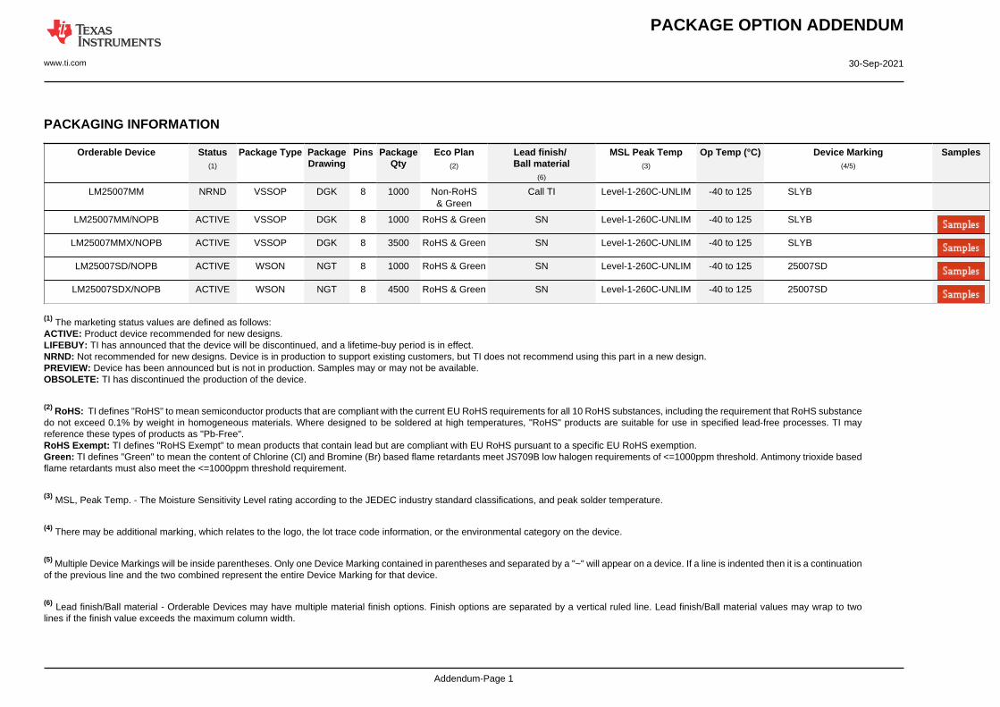
PACKAGE OPTION ADDENDUM
www.ti.com 30-Sep-2021
Addendum-Page 1
PACKAGING INFORMATION
Orderable Device Status(1)
Package Type PackageDrawing
Pins PackageQty
Eco Plan(2)
Lead finish/Ball material
(6)
MSL Peak Temp(3)
Op Temp (°C) Device Marking(4/5)
Samples
LM25007MM NRND VSSOP DGK 8 1000 Non-RoHS& Green
Call TI Level-1-260C-UNLIM -40 to 125 SLYB
LM25007MM/NOPB ACTIVE VSSOP DGK 8 1000 RoHS & Green SN Level-1-260C-UNLIM -40 to 125 SLYB
LM25007MMX/NOPB ACTIVE VSSOP DGK 8 3500 RoHS & Green SN Level-1-260C-UNLIM -40 to 125 SLYB
LM25007SD/NOPB ACTIVE WSON NGT 8 1000 RoHS & Green SN Level-1-260C-UNLIM -40 to 125 25007SD
LM25007SDX/NOPB ACTIVE WSON NGT 8 4500 RoHS & Green SN Level-1-260C-UNLIM -40 to 125 25007SD
(1) The marketing status values are defined as follows:ACTIVE: Product device recommended for new designs.LIFEBUY: TI has announced that the device will be discontinued, and a lifetime-buy period is in effect.NRND: Not recommended for new designs. Device is in production to support existing customers, but TI does not recommend using this part in a new design.PREVIEW: Device has been announced but is not in production. Samples may or may not be available.OBSOLETE: TI has discontinued the production of the device.
(2) RoHS: TI defines "RoHS" to mean semiconductor products that are compliant with the current EU RoHS requirements for all 10 RoHS substances, including the requirement that RoHS substancedo not exceed 0.1% by weight in homogeneous materials. Where designed to be soldered at high temperatures, "RoHS" products are suitable for use in specified lead-free processes. TI mayreference these types of products as "Pb-Free".RoHS Exempt: TI defines "RoHS Exempt" to mean products that contain lead but are compliant with EU RoHS pursuant to a specific EU RoHS exemption.Green: TI defines "Green" to mean the content of Chlorine (Cl) and Bromine (Br) based flame retardants meet JS709B low halogen requirements of <=1000ppm threshold. Antimony trioxide basedflame retardants must also meet the <=1000ppm threshold requirement.
(3) MSL, Peak Temp. - The Moisture Sensitivity Level rating according to the JEDEC industry standard classifications, and peak solder temperature.
(4) There may be additional marking, which relates to the logo, the lot trace code information, or the environmental category on the device.
(5) Multiple Device Markings will be inside parentheses. Only one Device Marking contained in parentheses and separated by a "~" will appear on a device. If a line is indented then it is a continuationof the previous line and the two combined represent the entire Device Marking for that device.
(6) Lead finish/Ball material - Orderable Devices may have multiple material finish options. Finish options are separated by a vertical ruled line. Lead finish/Ball material values may wrap to twolines if the finish value exceeds the maximum column width.

PACKAGE OPTION ADDENDUM
www.ti.com 30-Sep-2021
Addendum-Page 2
Important Information and Disclaimer:The information provided on this page represents TI's knowledge and belief as of the date that it is provided. TI bases its knowledge and belief on informationprovided by third parties, and makes no representation or warranty as to the accuracy of such information. Efforts are underway to better integrate information from third parties. TI has taken andcontinues to take reasonable steps to provide representative and accurate information but may not have conducted destructive testing or chemical analysis on incoming materials and chemicals.TI and TI suppliers consider certain information to be proprietary, and thus CAS numbers and other limited information may not be available for release.
In no event shall TI's liability arising out of such information exceed the total purchase price of the TI part(s) at issue in this document sold by TI to Customer on an annual basis.
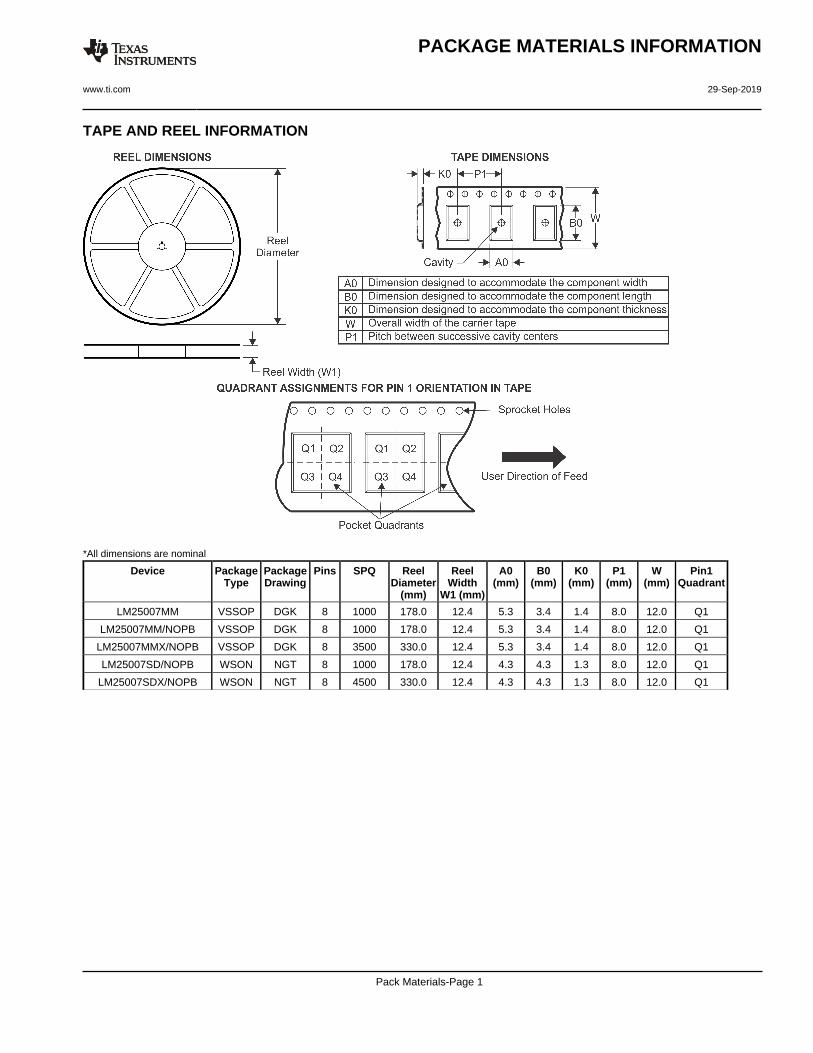
TAPE AND REEL INFORMATION
*All dimensions are nominal
Device PackageType
PackageDrawing
Pins SPQ ReelDiameter
(mm)
ReelWidth
W1 (mm)
A0(mm)
B0(mm)
K0(mm)
P1(mm)
W(mm)
Pin1Quadrant
LM25007MM VSSOP DGK 8 1000 178.0 12.4 5.3 3.4 1.4 8.0 12.0 Q1
LM25007MM/NOPB VSSOP DGK 8 1000 178.0 12.4 5.3 3.4 1.4 8.0 12.0 Q1
LM25007MMX/NOPB VSSOP DGK 8 3500 330.0 12.4 5.3 3.4 1.4 8.0 12.0 Q1
LM25007SD/NOPB WSON NGT 8 1000 178.0 12.4 4.3 4.3 1.3 8.0 12.0 Q1
LM25007SDX/NOPB WSON NGT 8 4500 330.0 12.4 4.3 4.3 1.3 8.0 12.0 Q1
PACKAGE MATERIALS INFORMATION
www.ti.com 29-Sep-2019
Pack Materials-Page 1

*All dimensions are nominal
Device Package Type Package Drawing Pins SPQ Length (mm) Width (mm) Height (mm)
LM25007MM VSSOP DGK 8 1000 210.0 185.0 35.0
LM25007MM/NOPB VSSOP DGK 8 1000 210.0 185.0 35.0
LM25007MMX/NOPB VSSOP DGK 8 3500 367.0 367.0 35.0
LM25007SD/NOPB WSON NGT 8 1000 210.0 185.0 35.0
LM25007SDX/NOPB WSON NGT 8 4500 367.0 367.0 35.0
PACKAGE MATERIALS INFORMATION
www.ti.com 29-Sep-2019
Pack Materials-Page 2

www.ti.com
PACKAGE OUTLINE
C
8X 0.350.25
3 0.052X2.4
2.6 0.05
6X 0.8
0.8 MAX
0.050.00
8X 0.50.3
A 4.13.9
B
4.13.9
(0.2) TYP
WSON - 0.8 mm max heightNGT0008APLASTIC SMALL OUTLINE - NO LEAD
4214935/A 08/2020
PIN 1 INDEX AREA
SEATING PLANE
0.08 C
1
4 5
8
PIN 1 ID0.1 C A B0.05 C
THERMAL PADEXPOSED
SYMM
SYMM9
NOTES: 1. All linear dimensions are in millimeters. Any dimensions in parenthesis are for reference only. Dimensioning and tolerancing per ASME Y14.5M. 2. This drawing is subject to change without notice. 3. The package thermal pad must be soldered to the printed circuit board for thermal and mechanical performance.
SCALE 3.000
www.ti.com
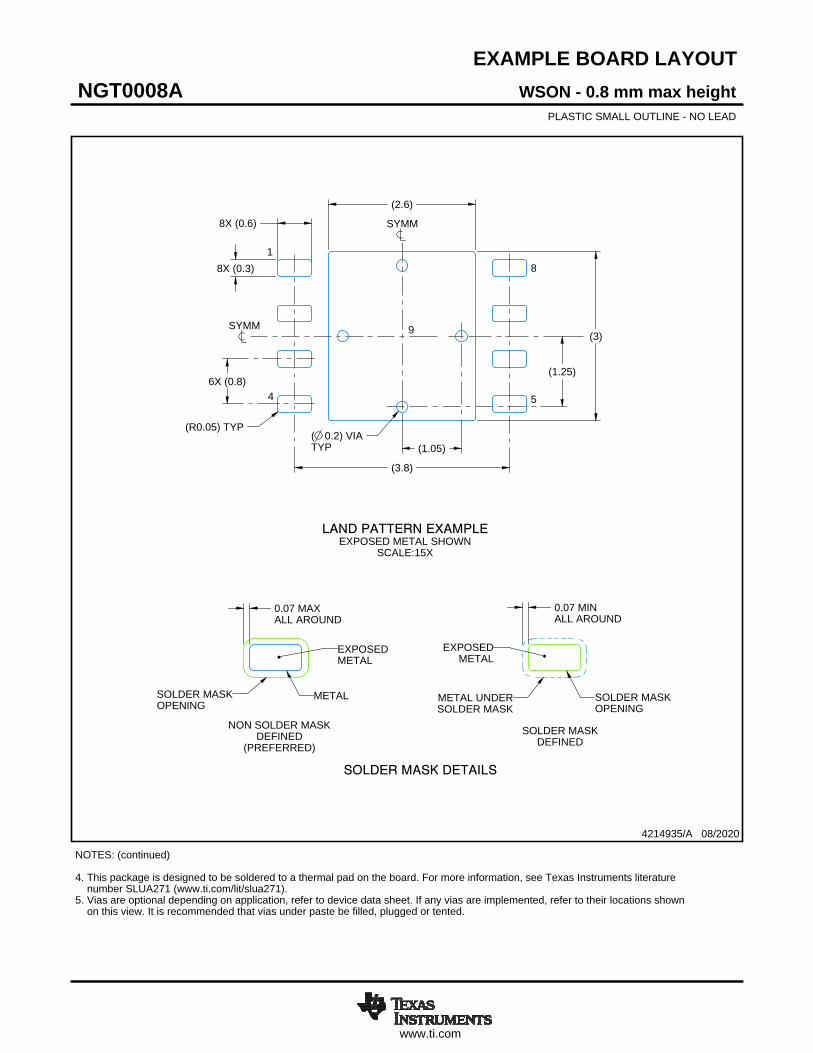
EXAMPLE BOARD LAYOUT
0.07 MINALL AROUND
0.07 MAXALL AROUND
8X (0.3)
(3)
(3.8)
6X (0.8)
(2.6)
( 0.2) VIATYP (1.05)
(1.25)
8X (0.6)
(R0.05) TYP
WSON - 0.8 mm max heightNGT0008APLASTIC SMALL OUTLINE - NO LEAD
4214935/A 08/2020
SYMM
1
4 5
8
LAND PATTERN EXAMPLEEXPOSED METAL SHOWN
SCALE:15X
SYMM 9
NOTES: (continued) 4. This package is designed to be soldered to a thermal pad on the board. For more information, see Texas Instruments literature number SLUA271 (www.ti.com/lit/slua271).5. Vias are optional depending on application, refer to device data sheet. If any vias are implemented, refer to their locations shown on this view. It is recommended that vias under paste be filled, plugged or tented.
SOLDER MASKOPENINGSOLDER MASK
METAL UNDER
SOLDER MASKDEFINED
EXPOSEDMETAL
METALSOLDER MASKOPENING
SOLDER MASK DETAILS
NON SOLDER MASKDEFINED
(PREFERRED)
EXPOSEDMETAL

www.ti.com
EXAMPLE STENCIL DESIGN
(R0.05) TYP
(1.31)
(0.675)
8X (0.3)
8X (0.6)
(1.15)
(3.8)
(0.755)
6X (0.8)
WSON - 0.8 mm max heightNGT0008APLASTIC SMALL OUTLINE - NO LEAD
4214935/A 08/2020
NOTES: (continued) 6. Laser cutting apertures with trapezoidal walls and rounded corners may offer better paste release. IPC-7525 may have alternate design recommendations.
SOLDER PASTE EXAMPLEBASED ON 0.125 mm THICK STENCIL
EXPOSED PAD 9:
77% PRINTED SOLDER COVERAGE BY AREA UNDER PACKAGESCALE:20X
SYMM
1
4 5
8
METALTYP
SYMM 9


IMPORTANT NOTICE AND DISCLAIMERTI PROVIDES TECHNICAL AND RELIABILITY DATA (INCLUDING DATASHEETS), DESIGN RESOURCES (INCLUDING REFERENCEDESIGNS), APPLICATION OR OTHER DESIGN ADVICE, WEB TOOLS, SAFETY INFORMATION, AND OTHER RESOURCES “AS IS”AND WITH ALL FAULTS, AND DISCLAIMS ALL WARRANTIES, EXPRESS AND IMPLIED, INCLUDING WITHOUT LIMITATION ANYIMPLIED WARRANTIES OF MERCHANTABILITY, FITNESS FOR A PARTICULAR PURPOSE OR NON-INFRINGEMENT OF THIRDPARTY INTELLECTUAL PROPERTY RIGHTS.These resources are intended for skilled developers designing with TI products. You are solely responsible for (1) selecting the appropriateTI products for your application, (2) designing, validating and testing your application, and (3) ensuring your application meets applicablestandards, and any other safety, security, or other requirements. These resources are subject to change without notice. TI grants youpermission to use these resources only for development of an application that uses the TI products described in the resource. Otherreproduction and display of these resources is prohibited. No license is granted to any other TI intellectual property right or to any third partyintellectual property right. TI disclaims responsibility for, and you will fully indemnify TI and its representatives against, any claims, damages,costs, losses, and liabilities arising out of your use of these resources.TI’s products are provided subject to TI’s Terms of Sale (https:www.ti.com/legal/termsofsale.html) or other applicable terms available eitheron ti.com or provided in conjunction with such TI products. TI’s provision of these resources does not expand or otherwise alter TI’sapplicable warranties or warranty disclaimers for TI products.IMPORTANT NOTICE
Mailing Address: Texas Instruments, Post Office Box 655303, Dallas, Texas 75265Copyright © 2021, Texas Instruments Incorporated