ELCODIS.COM - ELECTRONIC COMPONENTS...
26
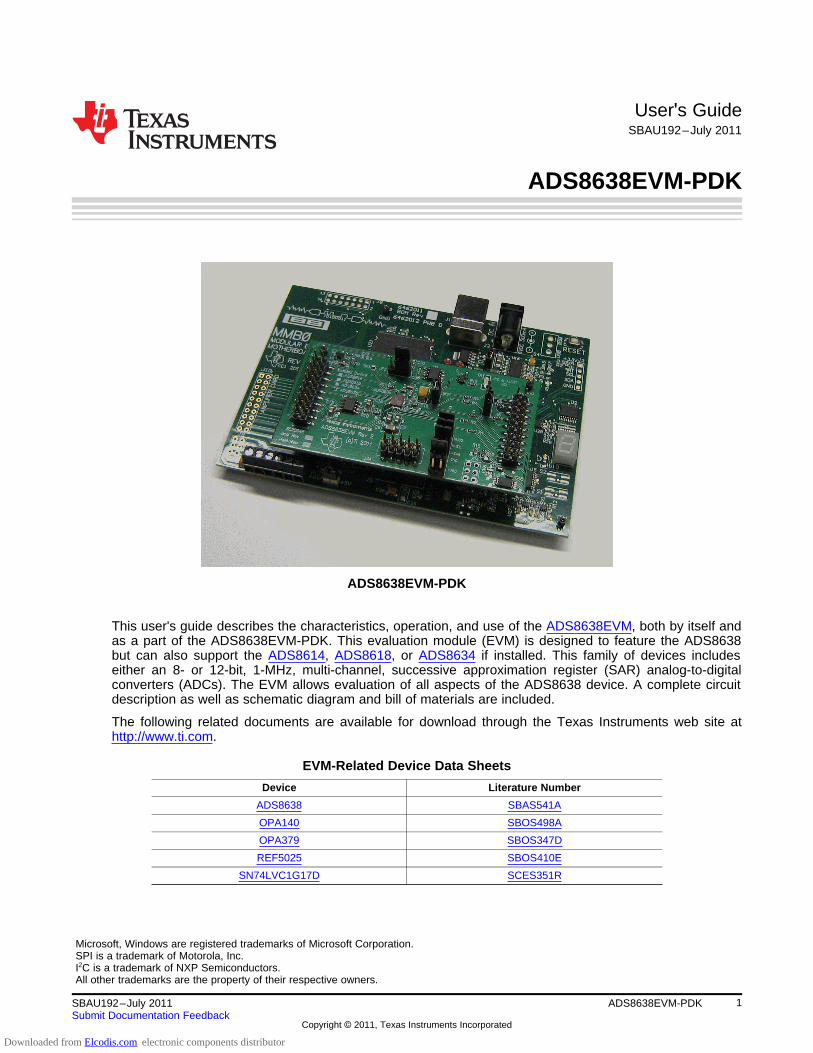
User's Guide SBAU192 – July 2011 ADS8638EVM-PDK ADS8638EVM-PDK This user's guide describes the characteristics, operation, and use of the ADS8638EVM, both by itself and as a part of the ADS8638EVM-PDK. This evaluation module (EVM) is designed to feature the ADS8638 but can also support the ADS8614, ADS8618, or ADS8634 if installed. This family of devices includes either an 8- or 12-bit, 1-MHz, multi-channel, successive approximation register (SAR) analog-to-digital converters (ADCs). The EVM allows evaluation of all aspects of the ADS8638 device. A complete circuit description as well as schematic diagram and bill of materials are included. The following related documents are available for download through the Texas Instruments web site at http://www.ti.com. EVM-Related Device Data Sheets Device Literature Number ADS8638 SBAS541A OPA140 SBOS498A OPA379 SBOS347D REF5025 SBOS410E SN74LVC1G17D SCES351R Microsoft, Windows are registered trademarks of Microsoft Corporation. SPI is a trademark of Motorola, Inc. I 2 C is a trademark of NXP Semiconductors. All other trademarks are the property of their respective owners. 1 SBAU192 – July 2011 ADS8638EVM-PDK Submit Documentation Feedback Copyright © 2011, Texas Instruments Incorporated Downloaded from Elcodis.com electronic components distributor
-
Upload
nguyentram -
Category
Documents
-
view
217 -
download
0
Transcript of ELCODIS.COM - ELECTRONIC COMPONENTS...
User's GuideSBAU192–July 2011
ADS8638EVM-PDK
ADS8638EVM-PDK
This user's guide describes the characteristics, operation, and use of the ADS8638EVM, both by itself andas a part of the ADS8638EVM-PDK. This evaluation module (EVM) is designed to feature the ADS8638but can also support the ADS8614, ADS8618, or ADS8634 if installed. This family of devices includeseither an 8- or 12-bit, 1-MHz, multi-channel, successive approximation register (SAR) analog-to-digitalconverters (ADCs). The EVM allows evaluation of all aspects of the ADS8638 device. A complete circuitdescription as well as schematic diagram and bill of materials are included.
The following related documents are available for download through the Texas Instruments web site athttp://www.ti.com.
EVM-Related Device Data Sheets
Device Literature Number
ADS8638 SBAS541A
OPA140 SBOS498A
OPA379 SBOS347D
REF5025 SBOS410E
SN74LVC1G17D SCES351R
Microsoft, Windows are registered trademarks of Microsoft Corporation.SPI is a trademark of Motorola, Inc.I2C is a trademark of NXP Semiconductors.All other trademarks are the property of their respective owners.
1SBAU192–July 2011 ADS8638EVM-PDKSubmit Documentation Feedback
Copyright © 2011, Texas Instruments Incorporated
Downloaded from Elcodis.com electronic components distributor

www.ti.com
Contents1 EVM Overview ............................................................................................................... 32 Analog Interface ............................................................................................................. 43 Digital Interface .............................................................................................................. 54 Power Supplies .............................................................................................................. 55 EVM Operation .............................................................................................................. 66 ADS8638EVM-PDK Kit Operation ........................................................................................ 77 Evaluating Performance with the ADCPro Software .................................................................. 148 EVM Bill of Materials, Schematic, and Layout ......................................................................... 20
List of Figures
1 ADS8638EVM Default Jumper Locations................................................................................ 7
2 ADS8638EVM-PDK Installer .............................................................................................. 8
3 Completed ADS8638EVM-PDK Installer................................................................................. 8
4 MMB0 Initial Setup.......................................................................................................... 9
5 Connecting ADS8638EVM to MMB0 ................................................................................... 10
6 Laboratory Power-Supply Connections................................................................................. 11
7 NI-VISA Driver Installation................................................................................................ 12
8 ADS86xxEVM-PDK Plug-in .............................................................................................. 13
9 Device Configuration ...................................................................................................... 15
10 Channels Tabs............................................................................................................. 17
11 GPIOs & Alarms Tab...................................................................................................... 18
12 ADS8638EVM PCB: Top Layer ......................................................................................... 21
13 ADS8638EVM PCB: Mid Layer.......................................................................................... 22
14 ADS8638EVM PCB: Ground Layer ..................................................................................... 22
15 ADS8638EVM PCB: Bottom Layer...................................................................................... 23
List of Tables
1 J1: Analog Interface Header............................................................................................... 4
2 J2: Serial Interface Header ................................................................................................ 5
3 J3: Power-Supply Interface Header ...................................................................................... 5
4 JP3 Configuration: Power Options........................................................................................ 6
5 Bill of Materials ............................................................................................................ 20
2 ADS8638EVM-PDK SBAU192–July 2011Submit Documentation Feedback
Copyright © 2011, Texas Instruments Incorporated
Downloaded from Elcodis.com electronic components distributor
www.ti.com EVM Overview
1 EVM Overview
1.1 Features
ADS8638EVM:• Full-featured evaluation board for the ADS8638 SAR ADC• Contains all support circuitry needed for the ADS8638• Optional onboard external REF5025 reference source• Compatible with the TI Modular EVM System
ADS8638EVM-PDK:• Easy-to-use evaluation software for Microsoft® Windows® XP operating system• Data collection to text files• Built-in analysis tools including scope, FFT, and histogram displays• Complete control of board settings• Easily expandable with new analysis plug-in tools from Texas Instruments
For use with a computer, the ADS8638EVM-PDK is also available. This kit combines the ADS8638 boardwith the DSP-based MMB0 motherboard, and includes ADCPro software for evaluation.
The MMB0 motherboard allows the ADS8638EVM to be connected to the computer via an available USBport. This manual shows how to use the MMB0 as part of the ADS8638EVMPDK, but does not providetechnical details about the MMB0 itself.
ADCPro is a program for collecting, recording, and analyzing data from ADC evaluation boards. It is basedon a number of plug-in programs, so it can be expanded easily with new test and data collection plug-ins.The ADS8638EVM-PDK is controlled by a plug-in running in ADCPro. For more information aboutADCPro, see the ADCPro™ Analog-to-Digital Converter Evalutation Software User's Guide (literaturenumber SBAU128), available for download from the TI web site.
This manual covers the operation of both the ADS8638EVM and the ADS8638EVM-PDK. Throughout thisdocument, the abbreviation EVM and the term evaluation module are synonymous with theADS8638EVM. For clarity of reading, the rest of this manual will refer only to the ADS8638EVM orADS8638EVM-PDK, but operation of the EVM and kit for the ADS8614, ADS8618, and ADS8634 isidentical, unless otherwise noted.
1.2 Introduction
The ADS8638 is a 12-bit, eight-channel, 1-MHz SAR ADC with a serial peripheral interface ( SPI™). TheADC uses a capacitor-based switching method to create an adjustable input voltage range option.Additionally, the device features two preset alarms with hysteresis per channel. During normal operation,the ADS8638 dissipates a mere 22.5 mW at 5-V AVDD and ±15-V high voltage supplies.
The ADS8638EVM is an evaluation module built to the TI Modular EVM System specification. It can beconnected to any modular EVM system interface card.
The ADS8638EVM is available as a stand-alone printed circuit board (PCB) or as part of theADS8638EVM-PDK, which includes an MMB0 motherboard and software. As a stand-alone PCB, theADS8638EVM is useful for evaluating designs and firmware.
Note that the ADS8638EVM has no microprocessor and cannot run software. To connect it to a computer,some type of interface is required.
3SBAU192–July 2011 ADS8638EVM-PDKSubmit Documentation Feedback
Copyright © 2011, Texas Instruments Incorporated
Downloaded from Elcodis.com electronic components distributor
Analog Interface www.ti.com
2 Analog Interface
For maximum flexibility, the ADS8638EVM is designed for easy interfacing to multiple analog sources.Samtec part numbers SSW-110-22-F-D-VS-K and TSM-110-01-T-DV-P provide a convenient 10-pin, dualrow header/socket combination at J1. This header/socket provides access to the analog input pins of theADC. Consult Samtec at www.samtec.com or call 1-800-SAMTEC-9 for a variety of mating connectoroptions. Table 1 shows the pinout of the analog input connector, J1.
Table 1. J1: Analog Interface Header
Pin Number Signal Description
J1.2 AIN7 / NC ADC analog input (AIN7: ADS8x38, NC: ADS8x34)
J1.4 AIN6 / NC ADC analog input (AIN6: ADS8x38, NC: ADS8x34)
J1.6 AIN5 / AIN3 ADC analog input (AIN5: ADS8x38, AIN3:ADS8x34)
J1.8 AIN4 / AIN2 ADC analog input (AIN4: ADS8x38, AIN2:ADS8x34)
J1.10 AIN3 / AIN1 ADC analog input (AIN3: ADS8x38, AIN1:ADS8x34)
J1.12 AIN2 / AIN0 ADC analog input (AIN2: ADS8x38, AIN0:ADS8x34)
J1.14 AIN1 / NC ADC analog input (AIN1: ADS8x38, NC: ADS8x34)
J1.16 AIN0 / NC ADC analog input (AIN0: ADS8x38, NC: ADS8x34)
J1.1-19 (odd) GND Analog ground connections (except J1.15)
J1.15 VREFOUT Buffered reference output
J1.18 NC —J1.20 Ext VREF External reference voltage input
The eight ADC analog inputs (four inputs for ADS8x34 devices) are available at the J1 header. All of theseinputs, with the exception of one, are routed directly from the J1 header to the ADC. The AIN2/AIN0channel includes an OPA140 to help drive one of the analog input channels to show the proper way todrive the ADC. The op amp is in unity gain, and includes a RC low-pass filter component before reachingthe ADC.
An external reference can be applied to the ADC via an external source using pin J1.20. This signal isrouted directly to JP2 where it can be jumped in to the VREFP line.
An OPA379 is located on the EVM to buffer the reference signal and output it on J1.15.
4 ADS8638EVM-PDK SBAU192–July 2011Submit Documentation Feedback
Copyright © 2011, Texas Instruments Incorporated
Downloaded from Elcodis.com electronic components distributor

www.ti.com Digital Interface
3 Digital Interface
3.1 Serial Data Interface
Samtec part numbers SSW-110-22-F-D-VS-K and TSM-110-01-T-DV-P provide a convenient 10-pin, dualrow header/socket combination at J2. This header/socket provides access to the digital control pins of theEVM. Consult Samtec at www.samtec.com or 1-800-SAMTEC- 9 for a variety of mating connector options.
Table 2 describes the J2 serial interface pins.
Table 2. J2: Serial Interface Header
Pin Number Signal Description
J2.1 CS ADC CS signal: controlled by jumper JP1
J2.2 GPIO ADC PD / Alert signal
J2.3 SCLK ADC SCLK signal
J2.4 GND Digital ground
J2.5 SCLK ADC SCLK signal
J2.7 CS ADC CS signal: controlled by jumper JP1
J2.9 CS ADC CS signal: controlled by jumper JP1
J2.10 GND Digital ground
J2.11 SDI ADC SDI signal
J2.13 SDO ADC SDO signal
J2.16 SCL I2C™ clock line for EEPROM
J2.18 GND Digital ground
J2.20 SDA I2C data line for EEPROM
4 Power Supplies
J3 is the power-supply input connector. Table 3 lists the configuration details for J3.
Table 3. J3: Power-Supply Interface Header
Pin Number Pin Name Function Required
J3.1 +VA High voltage positive Yesanalog supply
J3.2 –VA High voltage negative Yesanalog supply
J3.3 +5VA 5-V analog supply Yes
J3.4 –5VA Unused No
J3.5 GND Digital ground input Yes
J3.6 GND Analog ground input Yes
J3.7 +1.8VD 1.8-V digital supply Yes/Optional
J3.8 VD1 Unused No
J3.9 +3.3VD 3.3-V digital supply Yes/Optional
J3.10 +5VD Unused Yes/Optional
5SBAU192–July 2011 ADS8638EVM-PDKSubmit Documentation Feedback
Copyright © 2011, Texas Instruments Incorporated
Downloaded from Elcodis.com electronic components distributor

EVM Operation www.ti.com
4.1 Power Options
JP3 is in place for current measurement in order to regulate the power consumption of the ADS8638.When current measurement is not taking place, jumpers must be applied across many of the jumpers toproperly power the ADC. Table 4 lists the power option details for JP3.
Table 4. JP3 Configuration: Power Options
Row Name Function
1-2 ADC HVDD Supply current measurement point for highvoltage positive rail. Must be connected foroperation.
3-4 ADC HVEE Supply current measurement point for highvoltage negative rail. Must be connected foroperation.
5-6 ADC +5 VA Supply current measurement point for+5-VA voltage rail. Must be connected foroperation.
7-8 GND Ground points for EVM board
9-10 ADC +3.3 VD Supply current measurement point for 3.3-Vdigital supply rail. Must be connected forADC use with DVDD = 3.3 V. Do notconnect if +5-VD jumper is installed.
11-12 ADC +1.8 VD Supply current measurement point for 1.8Vdigital supply rail. Must be connected forADC use with DVDD = 1.8 V. Do notconnect if +3.3-VD jumper is installed.
The ADS8638EVM has the option to either set +1.8 VD or +3.3 VD as the ADS8638 DVDD supply. Installa jumper across pins 9-10 to set DVDD = 3.3 V, or install a jumper across pins 11-12 to set DVDD =1.8 V.
CAUTION
Do not install both jumpers. Doing so may cause damage to the board or ADCdevice itself.
4.2 Reference Voltages
The ADS8638EVM can be configured to use the internal reference voltage found within the chip, anonboard REF5025 reference source, or use the option to input an external reference source. Jumper JP2is used to route the reference signal to the ADC. When placed in the 1-2 position, the onboard REF5025is used as the reference signal. When placed in the 2-3 position, an outside external reference can beapplied to J1.20 on the analog header to feed the ADC reference. If the ADC internal reference isenabled, the shunt on jumper JP2 must be either in the 2-3 position or left disconnected. Thisconfiguration ensures that the REF5025 source is not driving the ADS8638 reference pin when the pin isconfigured as an output.
5 EVM Operation
This section provides information on the analog input, digital control, and general operating conditions ofthe ADS8638EVM.
5.1 Analog Input
Each of the analog input sources can be applied directly to J1 (top or bottom side) or throughsignal-conditioning modules available for the modular EVM system.
6 ADS8638EVM-PDK SBAU192–July 2011Submit Documentation Feedback
Copyright © 2011, Texas Instruments Incorporated
Downloaded from Elcodis.com electronic components distributor
www.ti.com ADS8638EVM-PDK Kit Operation
5.2 Digital Control
The digital control signals can be applied directly to J2 (top or bottom side). The modular ADS8638EVMcan also be connected directly to a DSP or microcontroller interface board, such as the 5-6K Interface orHPA-MCU Interface boards available from Texas Instruments, or the MMB0 if purchased as part of theADS8638EVM-PDK. For a list of compatible interface and/or accessory boards for the EVM or theADS8638, see the relevant device product folder on the TI web site
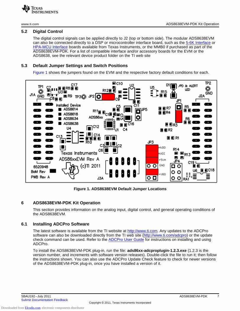
5.3 Default Jumper Settings and Switch Positions
Figure 1 shows the jumpers found on the EVM and the respective factory default conditions for each.
Figure 1. ADS8638EVM Default Jumper Locations
6 ADS8638EVM-PDK Kit Operation
This section provides information on the analog input, digital control, and general operating conditions ofthe ADS8638EVM.
6.1 Installing ADCPro Software
The latest software is available from the TI website at http://www.ti.com. Any updates to the ADCProsoftware can also be downloaded directly from the TI web site (http://www.ti.com/adcpro) or the updatecheck command can be used. Refer to the ADCPro User Guide for instructions on installing and usingADCPro.
To install the ADS8638EVM-PDK plug-in, run the file: ads86xx-adcproplugin-1.2.3.exe (1.2.3 is theversion number, and increments with software version releases). Double-click the file to run it; then followthe instructions shown. You can also use the ADCPro Update Check feature to check for newer versionsof the ADS8638EVM-PDK plug-in, once you have installed a version of it.
7SBAU192–July 2011 ADS8638EVM-PDKSubmit Documentation Feedback
Copyright © 2011, Texas Instruments Incorporated
Downloaded from Elcodis.com electronic components distributor
ADS8638EVM-PDK Kit Operation www.ti.com
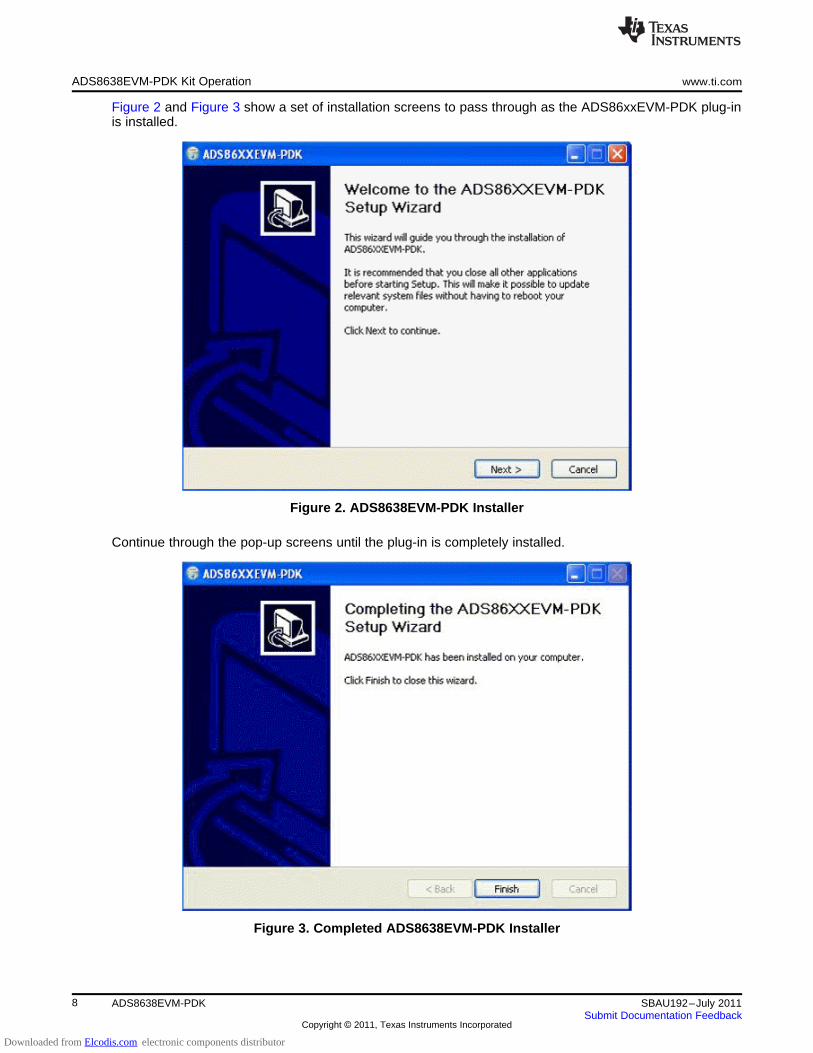
Figure 2 and Figure 3 show a set of installation screens to pass through as the ADS86xxEVM-PDK plug-inis installed.
Figure 2. ADS8638EVM-PDK Installer
Continue through the pop-up screens until the plug-in is completely installed.
Figure 3. Completed ADS8638EVM-PDK Installer
8 ADS8638EVM-PDK SBAU192–July 2011Submit Documentation Feedback
Copyright © 2011, Texas Instruments Incorporated
Downloaded from Elcodis.com electronic components distributor

www.ti.com ADS8638EVM-PDK Kit Operation
6.2 Setting Up the ADS8638EVM-PDK
The ADS8638EVM-PDK contains both the ADS8638EVM and the MMB0 motherboard; however, thedevices are shipped unconnected. Follow these steps to set up the ADS8638EVM-PDK.
Step 1. Unpack the ADS8638EVM-PDK kit.Step 2. Set the jumpers and switches on the MMB0 as shown in Figure 4.
• Set the Boot Mode switch to USB.• Connect +5 V and +5 VA on jumper block J13B (if +5 V is supplied from J14 +5 VA).• Leave +5 V and +VA disconnected on jumper block J13A.• If the PDK is powered from an ac adapter, connect J12. If the PDK is powered through
the terminal block, disconnect J12. (See Section 6.3 for details on connecting the powersupply.)
Figure 4. MMB0 Initial Setup
9SBAU192–July 2011 ADS8638EVM-PDKSubmit Documentation Feedback
Copyright © 2011, Texas Instruments Incorporated
Downloaded from Elcodis.com electronic components distributor
ADS8638EVM-PDK Kit Operation www.ti.com
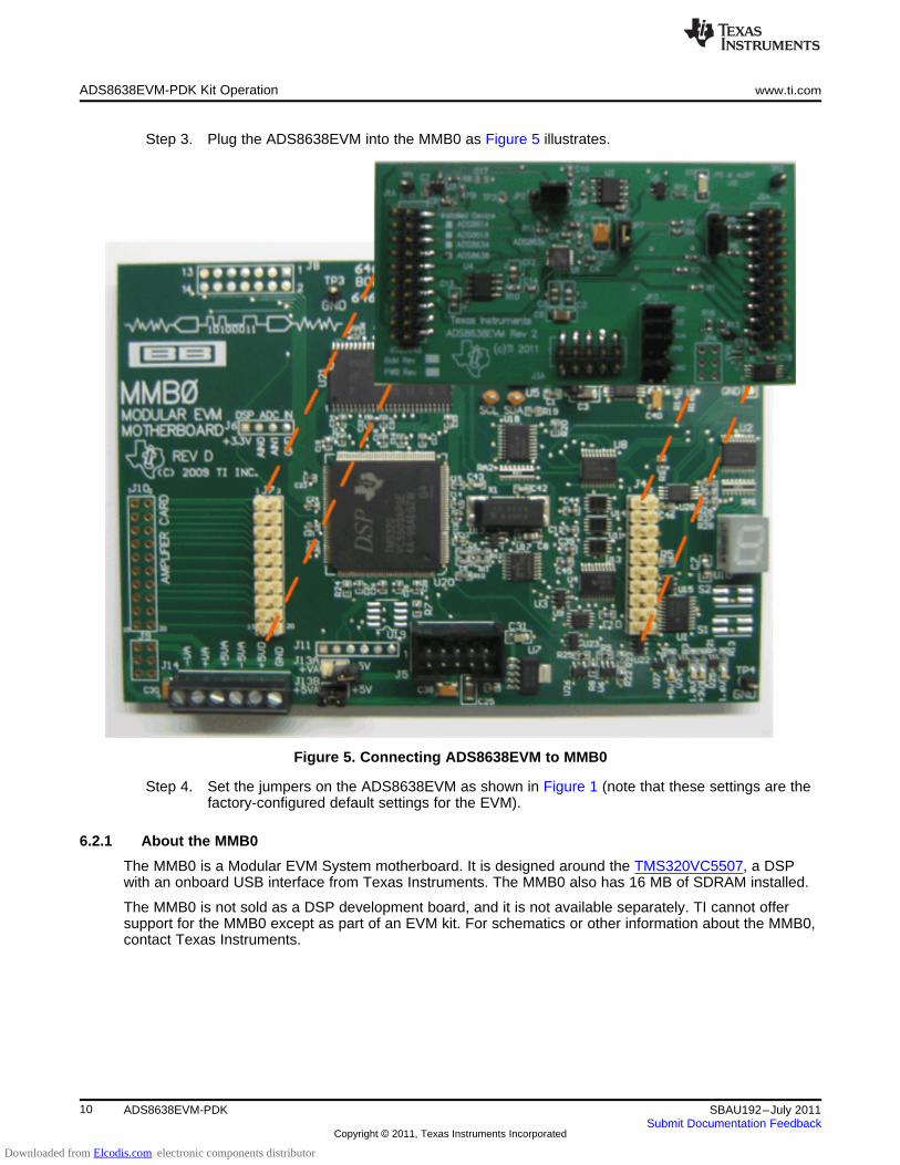
Step 3. Plug the ADS8638EVM into the MMB0 as Figure 5 illustrates.
Figure 5. Connecting ADS8638EVM to MMB0
Step 4. Set the jumpers on the ADS8638EVM as shown in Figure 1 (note that these settings are thefactory-configured default settings for the EVM).
6.2.1 About the MMB0
The MMB0 is a Modular EVM System motherboard. It is designed around the TMS320VC5507, a DSPwith an onboard USB interface from Texas Instruments. The MMB0 also has 16 MB of SDRAM installed.
The MMB0 is not sold as a DSP development board, and it is not available separately. TI cannot offersupport for the MMB0 except as part of an EVM kit. For schematics or other information about the MMB0,contact Texas Instruments.
10 ADS8638EVM-PDK SBAU192–July 2011Submit Documentation Feedback
Copyright © 2011, Texas Instruments Incorporated
Downloaded from Elcodis.com electronic components distributor
www.ti.com ADS8638EVM-PDK Kit Operation
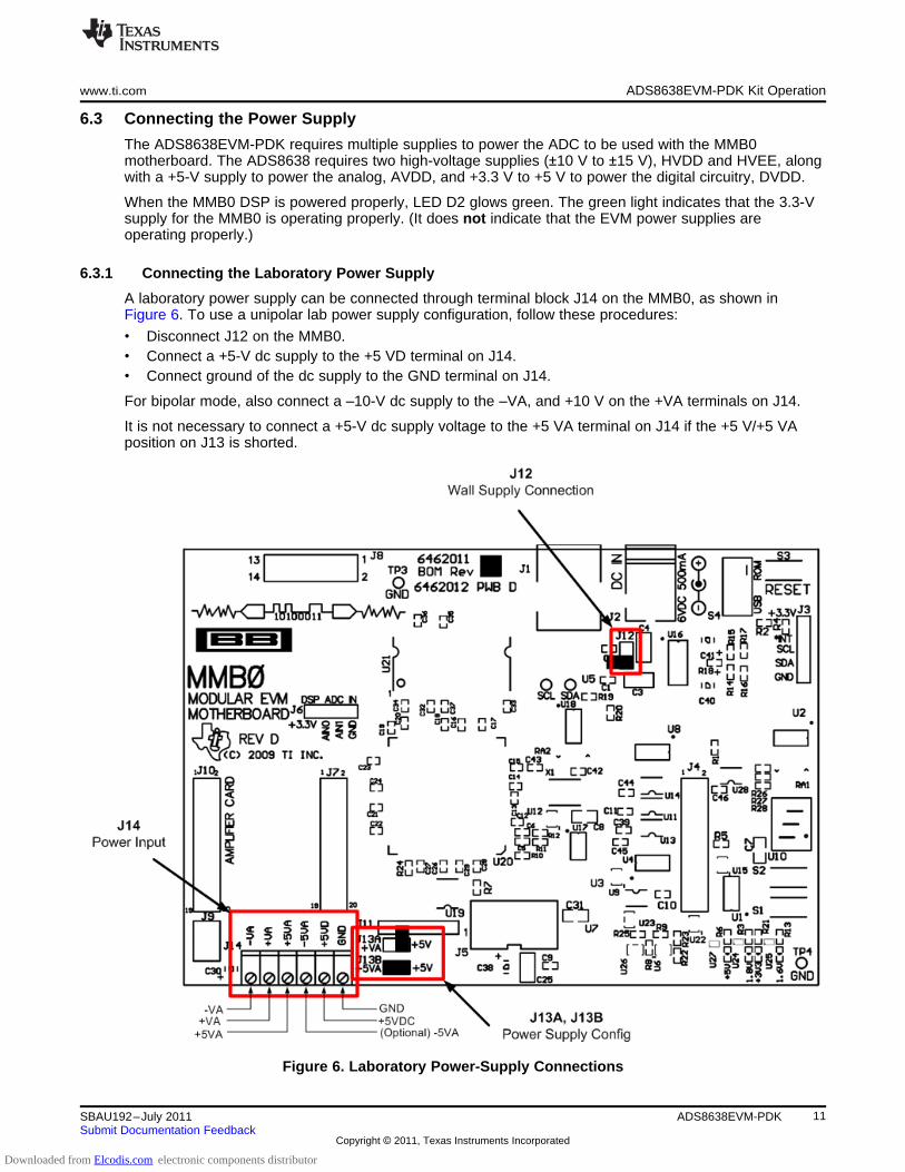
6.3 Connecting the Power Supply
The ADS8638EVM-PDK requires multiple supplies to power the ADC to be used with the MMB0motherboard. The ADS8638 requires two high-voltage supplies (±10 V to ±15 V), HVDD and HVEE, alongwith a +5-V supply to power the analog, AVDD, and +3.3 V to +5 V to power the digital circuitry, DVDD.
When the MMB0 DSP is powered properly, LED D2 glows green. The green light indicates that the 3.3-Vsupply for the MMB0 is operating properly. (It does not indicate that the EVM power supplies areoperating properly.)
6.3.1 Connecting the Laboratory Power Supply
A laboratory power supply can be connected through terminal block J14 on the MMB0, as shown inFigure 6. To use a unipolar lab power supply configuration, follow these procedures:
• Disconnect J12 on the MMB0.• Connect a +5-V dc supply to the +5 VD terminal on J14.• Connect ground of the dc supply to the GND terminal on J14.
For bipolar mode, also connect a –10-V dc supply to the –VA, and +10 V on the +VA terminals on J14.
It is not necessary to connect a +5-V dc supply voltage to the +5 VA terminal on J14 if the +5 V/+5 VAposition on J13 is shorted.
Figure 6. Laboratory Power-Supply Connections
11SBAU192–July 2011 ADS8638EVM-PDKSubmit Documentation Feedback
Copyright © 2011, Texas Instruments Incorporated
Downloaded from Elcodis.com electronic components distributor
ADS8638EVM-PDK Kit Operation www.ti.com
6.4 Running the Software and Completing Driver Installation
NOTE: The software is continually under development. These instructions and screen images arecurrent at the time of this writing, but may not exactly match future releases.
The program for evaluating the ADS8638EVM-PDK is called ADCPro. This program uses plug-ins tocommunicate with the EVM. The ADS8638EVM-PDK plug-in is included in the ADS8638EVM-PDKpackage.
The program currently runs only on Microsoft Windows platforms of Windows XP; plans are in place tohave ADCPro working on Windows 7 in the near future.
If this is the first time installing ADCPro and any related plug-ins, follow these procedures to run theADCPro software and complete the necessary driver installation. Make sure the ADCPro software anddevice plug-in software are the latest versions available online at www.ti.com/ADCPro.
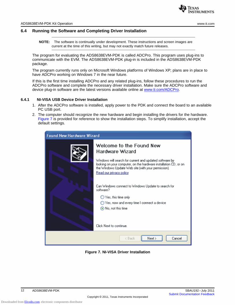
6.4.1 NI-VISA USB Device Driver Installation1. After the ADCPro software is installed, apply power to the PDK and connect the board to an available
PC USB port.2. The computer should recognize the new hardware and begin installing the drivers for the hardware.
Figure 7 is provided for reference to show the installation steps. To simplify installation, accept thedefault settings.
Figure 7. NI-VISA Driver Installation
12 ADS8638EVM-PDK SBAU192–July 2011Submit Documentation Feedback
Copyright © 2011, Texas Instruments Incorporated
Downloaded from Elcodis.com electronic components distributor
www.ti.com ADS8638EVM-PDK Kit Operation
6.4.2 USBStyx Driver Installation1. Start the software by selecting ADCPro from the Windows Start menu.2. Select ADS86xxEVM from the EVM drop-down menu. The ADS86xxEVM-PDK plug-in appears in the
left pane. The setup is shown in Figure 8.
Figure 8. ADS86xxEVM-PDK Plug-in
3. The ADS86xxEVM-PDK plug-in window has a status area at the top of the screen. When the plug-in isfirst loaded, the plug-in searches for the board. A series of messages will appear in the status area toindicate this action.
4. If you have not yet loaded the operating system drivers, Windows displays the Install New DriverWizard sequence; accept the default settings.
NOTE: During the driver installation process, a message may appear that indicates the firmwareload has timed out. Click OK and continue driver installation. The plug-in will attempt todownload the firmware again once the driver installation completes.
5. Once Windows finishes installing the software driver, the plug-in downloads the firmware to the MMB0.The status area displays Connected to EVM when the device is connected and ready to use. If thefirmware does not load properly, you can try resetting the MMB0 by pressing Reset and then reloadingthe plug-in.
13SBAU192–July 2011 ADS8638EVM-PDKSubmit Documentation Feedback
Copyright © 2011, Texas Instruments Incorporated
Downloaded from Elcodis.com electronic components distributor

Evaluating Performance with the ADCPro Software www.ti.com
7 Evaluating Performance with the ADCPro Software
The evaluation software is based on ADCPro, a program that operates using a variety of plug-ins. (TheADS8638EVM plug-in is installed as described in the Installation section).
To use ADCPro, load an EVM plug-in and a test plug-in. To load an EVM plug-in, select it from the EVMmenu. To load a test plug-in, select it from the Test menu. To unload a plug-in, select the Unload optionfrom the corresponding menu. Only one of each kind of plug-in can be loaded at a time. If you select adifferent plug-in, the previous plug-in is unloaded.
7.1 Using the ADS8638EVM-PDK Plug-in
The ADS8638EVM-PDK plug-in for ADCPro provides complete control over all settings of the ADS8638. Itconsists of a tabbed interface, with different functions available on different tabs. These controls aredescribed in this section.
You can adjust the ADS8638EVM settings when you are not acquiring data. During acquisition, allcontrols are disabled and settings may not be changed.
When you change a setting on the ADS8638EVM plug-in, the setting immediately updates on the board.Settings on the ADS8638EVM correspond to settings described in the ADS8638 product data sheet(available for download at www.ti.com).
14 ADS8638EVM-PDK SBAU192–July 2011Submit Documentation Feedback
Copyright © 2011, Texas Instruments Incorporated
Downloaded from Elcodis.com electronic components distributor
www.ti.com Evaluating Performance with the ADCPro Software
7.1.1 Plug-in Setup and The Device Config Tab
When the ADS86xxEVM plug-in is first loaded, you must select the device from the Device Selection tabfound in the basic settings window. The ADC options are not available on the plug-in until the device isselected. Use Figure 9 for reference.
Figure 9. Device Configuration
After the ADC has been selected, the tabs on the left become available, including the plug-in options toconfigure the ADC. The Device Config tab is the default window and includes some of the basic settingsto configure that ADC. Basic information, such as the Plug-in version and Firmware version, is shown herealong with some simple settings use to set up the ADC according to user preferences.
15SBAU192–July 2011 ADS8638EVM-PDKSubmit Documentation Feedback
Copyright © 2011, Texas Instruments Incorporated
Downloaded from Elcodis.com electronic components distributor

Evaluating Performance with the ADCPro Software www.ti.com
The Data Rate control on the main plug-in window sets the data rate for the ADS8638. Changing the datarate controls the time between sequential conversions once the acquisition period begins.
In the Basic Settings window, the Operating Mode and Input Range options are available. The plug-in wasdesigned to only use auto-mode channel sequencing, and therefore manual mode is not selectable. Theinput range option allows the user to select the desired analog input voltage range from +5 V, +10 V,±2.5 V, ±5 V, or ±10 V. This setting becomes the range for all the channels that are enabled at the time ofdata acquisition.
The Power Blocks window includes buttons to enable the internal reference voltage and the internaltemperature sensor. By default, these two options are disabled and are enabled once the appropriatebutton is selected.
The About this plug-in tab has the plug-in version history along with the firmware version. The Notesindicator shows manufacturing information about the EVM that is stored in the EVM EEPROM, and mayshow relevant notes about the plug-in or firmware code, if any.
At the bottom of the Device Config window is the PowerDown button. Use this button to direct theprocessor to write the command that puts the ADC into power-down mode.
7.1.2 Channels 1-4 Tab and 5-8 Tab
These two tabs, as shown in Figure 10, are used to enable/disable the ADC channels as well as configurethe alarm states. By default, all of the eight channels are disabled. Before an acquisition can beperformed, at least one channel must be enabled. Once a channel is enabled, the alarm high and alarmlow thresholds can be set along with the respective hysteresis limits. As the converted result exceeds thealarm threshold, the LED found on the EVM board should turn on to indicate an alarm.
As multiple channels are enabled, the effective data rate decreases. The ADS8638 uses an architecturethat relies on an internal cycling mux, requiring the conversions to be completed in a sequential orderrather than simultaneously. The data rate displayed in the top right corner of the plugin refers to allenabled channels to be converted.
16 ADS8638EVM-PDK SBAU192–July 2011Submit Documentation Feedback
Copyright © 2011, Texas Instruments Incorporated
Downloaded from Elcodis.com electronic components distributor

www.ti.com Evaluating Performance with the ADCPro Software
Figure 10. Channels Tabs
17SBAU192–July 2011 ADS8638EVM-PDKSubmit Documentation Feedback
Copyright © 2011, Texas Instruments Incorporated
Downloaded from Elcodis.com electronic components distributor

Evaluating Performance with the ADCPro Software www.ti.com
7.1.3 GPIO & Alarms Tab
The GPIO & Alarms tab (as shown in Figure 11) includes some of the additional options found within theADS8638. Here, the software provides access to setting the GPIO as either a power-down input or analarm state output. This I/O line is routed to the onboard LED on the evaluation board to indicate when thealarm is active.
Figure 11. GPIOs & Alarms Tab
The Temperature control is used to read back the temperature control and enable high and low alarmsalong with hysteresis. When reading back the temperature reading, the result is read back in codes whereit must be converted to a temperature using the parameters described in the ADS8638 product data sheet.The high and low alarms, along with hysteresis settings, behave the same way that the analog inputchannel alarm settings do.
18 ADS8638EVM-PDK SBAU192–July 2011Submit Documentation Feedback
Copyright © 2011, Texas Instruments Incorporated
Downloaded from Elcodis.com electronic components distributor

www.ti.com Evaluating Performance with the ADCPro Software
After an acquisition, the Read Alarms button allows the user to read back the specific alarms thatreported a fault. When the button is pressed, the firmware uses the sticky register read command; oncethe alarms are read, they are set back to zero. Each channel has two alarms, a high alarm and a lowalarm; both are placed side by side in the alarm list. When the Read Alarms button is pressed, the LEDcorresponding to the alarm limit that was breached is enabled.
7.1.4 Collecting Data
Once you have configured the ADS8638 for your test scenario, press the ADCPro Acquire button to startthe collection of the number of data points specified in the Test plug-in Block Size control. TheADS8638EVM-PDK plug-in disables all the front panel controls while acquiring, and displays a progressbar.
7.2 Troubleshooting
If ADCPro stops responding while the ADS8638EVM-PDK is connected, try unplugging the power supplyfrom the PDK. Unload and reload the plug-in before reapplying power to the PDK.
19SBAU192–July 2011 ADS8638EVM-PDKSubmit Documentation Feedback
Copyright © 2011, Texas Instruments Incorporated
Downloaded from Elcodis.com electronic components distributor

EVM Bill of Materials, Schematic, and Layout www.ti.com
8 EVM Bill of Materials, Schematic, and Layout
Table 5 contains a complete bill of materials for the modular ADS8638EVM. The schematic diagram isalso provided for reference. Figure 12 through Figure 15 show the PCB layouts.
8.1 Parts List
NOTE: All components should be compliant with the European Union Restriction on Use ofHazardous Substances (RoHS) Directive. Some part numbers may be either leaded orRoHS. Verify that purchased components are RoHS-compliant. (For more information aboutTI's position on RoHS compliance, see the Quality and Eco-Info information on the TI website.)
Table 5. Bill of Materials
Item Qty Ref Des Description MFR Part Number
1 1 N/A Printed wiring board n/a 6520948
2 3 C1, C4, Capacitor, ceramic, 1.0 µF 16V 10% X5R 0603 Murata GRM188R61C105KA93DC11
3 4 C2, C3, Capacitor, ceramic, 10 µF 16V X5R 0805 Murata GRM21BR61C106KE15LC12, C13
4 4 C5, C8, Capacitor, ceramic, 0.1 µF 16V 10% X7R 0603 Murata GRM188R71C104KA01DC15, C18
5 1 C6 Capacitor, ceramic, 1 µF 50V X7R 1206 Murata GRM31CR71H105KA61L
6 3 C9, C10, Capacitor, ceramic, 10 µF 6.3V X5R 0603 Murata GRM188R60J106ME47DC19
7 0 C7, C17 Not installed
8 1 C14 Capacitor, ceramic, 1000 pF 50V 5% C0G 0603 Murata GRM1885C1H102JA01D
9 1 C16 Capacitor, tantalum, 10 µF 16V 10% SMD Kemet T494B106K016AT
10 1 D1 LED 565 nm, green diff 1206 SMD Lumex Opto SML-LX1206GW-TR
11 2 J1A, J2A 10-pin, dual row, SM Header (20 Pos.) Samtec TSM-110-01-T-DV-P(Top Side)
12 2 J1B, J2B 10-pin, dual row, SM Header (20 Pos.) Samtec SSW-110-22-F-D-VS-K(Bottom
Side)
13 1 J3A (Top 5-pin, dual row, SM Header (10 Pos.) Samtec TSM-105-01-T-DV-PSide)
14 1 J3B 5-pin, dual row, SM Header (10 Pos.) Samtec SSW-105-22-F-D-VS-K(Bottom
Side)
15 2 JP1, JP2 Header strip, 3-pin (1x3) Samtec TSW-103-07-L-S
16 1 JP3 Header ltrip, 12-pin (2x6) Samtec TSW-106-07-L-D
17 0 JP4 Not installed
18 1 JP5 2-position jumper _ .1" spacing Samtec TSW-102-07-T-S
19 4 R1, R2, R3, Resistor, 33 Ω 1/10W 5% 0603 SMD Panasonic ERJ-3GEYJ330VR4, R7
20 5 R5, R6, R8, Resistor, 0 Ω 1/10W 5% 0603 SMD Panasonic ERJ-3GEY0R00VR9, R12
21 2 R10, R11 Resistor, 20 Ω 1/10W 5% 0603 SMD Panasonic ERJ-3GEYJ200V
22 2 R13, R14 Resistor, 10 kΩ 1/10W 5% 0603 SMD Panasonic ERJ-3GEYJ103V
23 1 R15 Resistor, 470 Ω 1/10W 5% 0603 SMD Panasonic ERJ-3GEYJ471V
24 0 RA1 Not installed
25 2 TP1, TP2 Test point: single .025-Pin, Black Keystone 5001
26 1 TP3 Test point: single .025-Pin, Red Keystone 5000
27 1 U1 ADS8638, 8-channel 12-bit HV MUX SAR ADC Texas ADS8638SRGERSPI Instruments
20 ADS8638EVM-PDK SBAU192–July 2011Submit Documentation Feedback
Copyright © 2011, Texas Instruments Incorporated
Downloaded from Elcodis.com electronic components distributor

www.ti.com EVM Bill of Materials, Schematic, and Layout
Table 5. Bill of Materials (continued)
Item Qty Ref Des Description MFR Part Number
28 1 U2 Precision voltage reference 2.5 V, 8SOIC Texas REF5025AIDInstruments
29 1 U3 IC Op Amp GP R-R 90 kHz SOT23-5 Texas OPA379AIDBVTInstruments
30 1 U4 IC Op Amp GP R-R 80 MHz SGL 8SOIC Texas OPA140AIDInstruments
31 1 U5 Logic Single Schmitt-Trigger Buffer Texas SN74LVC1G17DBVRInstruments
32 1 U6 IC EEPROM 256Kbit 400 kHz 8TSSOP Microchip 24AA256-I/ST
33 6 N/A Shunt Jumper .1" Black gold 3M 969102-0000-DA
8.2 Board Layouts
NOTE: Board layouts are not to scale. These images are intended to show how the board is laidout; they are not intended to be used for manufacturing ADS8638EVM PCBs.
Figure 12. ADS8638EVM PCB: Top Layer
21SBAU192–July 2011 ADS8638EVM-PDKSubmit Documentation Feedback
Copyright © 2011, Texas Instruments Incorporated
Downloaded from Elcodis.com electronic components distributor
EVM Bill of Materials, Schematic, and Layout www.ti.com
Figure 13. ADS8638EVM PCB: Mid Layer
Figure 14. ADS8638EVM PCB: Ground Layer
22 ADS8638EVM-PDK SBAU192–July 2011Submit Documentation Feedback
Copyright © 2011, Texas Instruments Incorporated
Downloaded from Elcodis.com electronic components distributor

www.ti.com EVM Bill of Materials, Schematic, and Layout
Figure 15. ADS8638EVM PCB: Bottom Layer
23SBAU192–July 2011 ADS8638EVM-PDKSubmit Documentation Feedback
Copyright © 2011, Texas Instruments Incorporated
Downloaded from Elcodis.com electronic components distributor
1 2 3 4 5 6
A
B
C
D
654321
D
C
B
A
Title
Number RevisionSize
B
Date: 11-May-2011 Sheet of File: C:\Userdata\projects\ads8638\ADS8638EVM_RA.ddbDrawn By:
AV
DD
1
AGND2 AGND3
NC
4
AINCOM5
AIN7/NC6
AIN6/NC7
AIN5/AIN38
AIN2/AIN011
AIN4/AIN29
AIN3/AIN110
AIN1/NC12
AIN0/NC13 HV
DD
14
HV
EE15
CS 16
SCLK 17
SDI 18
SDO 19
DGND 20
DV
DD
21
PD/ALERT 22
VREFP 24
VREFM 23
U1
ADS86xx
A0(+) 2A1(+) 4A2(+) 6A3(+) 8A4 10A5 12A6 14A7 16REF- 18REF+ 20
A0(-)1 A1(-)3 A2(-)5 A3(-)7 AGND9 AGND11 AGND13 VCOM15 AGND17 AGND19J1A
DAUGHTER-ANALOG
-VA 2
-5VA 4
AGND 6
VD1 8
+5VD 10
+VA1
+5VA3
DGND5
+1.8VD7
+3.3VD9
J3A
DAUGHTER-POWER
GPIO0 2
DGND 4
GPIO1 6
GPIO2 8
DGND 10
GPIO3 12
GPIO4 14
SCL 16
DGND 18
SDA 20
CNTL1
CLKX3
CLKR5
FSX7
FSR9
DX11
DR13
INT15
TOUT17
GPIO519
J2A
DAUGHTER-SERIAL
R5 0
R6 0
JP1
VIN2 VOUT 6
TRIM 5GND4 TEMP3
U2
REF5025
C910uF C10
10uF
R12
0HVDD
HVEE+5V
+5V
HVEE HVDD
C210uF
C310uF
C11uF
TP1 TP2
JP2
C8
0.1uF
C7 DNI
R9 0
3
41
25
U3
OPA379
R8 0
+5VA
C4
1uF
+VBD
+5VA
2
36
74
U4
OPA140
R10
20C141nF
+VA
C1210uF
-VA
C1310uF
C111uF
R1
33R2
33
R3 33R4 33
R11 20TP3
+VBD
246
13578910
1112
JP3
HEADER-6X2
+VA -VA+5VA
C150.1uF
C6
1uF (50V rated)
C50.1uF
R7
33
R1310k
R1410k
+3.3VD
GPIO
GPIO
+ C1610uF
C17DNI A01
A12
GND 4
SDA 5
SCL 6
WP7
VCC 8
A23
U6
24AA256-I/ST
246
135
JP4
DNI
RA1DNI
C180.1uF
+3.3VD
+3.3VD
+3.3VD
JP5
ti
D1
R15470
Y 4
GND 3
VCC5
A2
NC 1
U5
SN74LVC1G17
+3.3VD
C1910uF
Downloaded from Elcodis.com electronic components distributor

Evaluation Board/Kit Important Notice
Texas Instruments (TI) provides the enclosed product(s) under the following conditions:
This evaluation board/kit is intended for use for ENGINEERING DEVELOPMENT, DEMONSTRATION, OR EVALUATIONPURPOSES ONLY and is not considered by TI to be a finished end-product fit for general consumer use. Persons handling theproduct(s) must have electronics training and observe good engineering practice standards. As such, the goods being provided arenot intended to be complete in terms of required design-, marketing-, and/or manufacturing-related protective considerations,including product safety and environmental measures typically found in end products that incorporate such semiconductorcomponents or circuit boards. This evaluation board/kit does not fall within the scope of the European Union directives regardingelectromagnetic compatibility, restricted substances (RoHS), recycling (WEEE), FCC, CE or UL, and therefore may not meet thetechnical requirements of these directives or other related directives.
Should this evaluation board/kit not meet the specifications indicated in the User’s Guide, the board/kit may be returned within 30days from the date of delivery for a full refund. THE FOREGOING WARRANTY IS THE EXCLUSIVE WARRANTY MADE BYSELLER TO BUYER AND IS IN LIEU OF ALL OTHER WARRANTIES, EXPRESSED, IMPLIED, OR STATUTORY, INCLUDINGANY WARRANTY OF MERCHANTABILITY OR FITNESS FOR ANY PARTICULAR PURPOSE.
The user assumes all responsibility and liability for proper and safe handling of the goods. Further, the user indemnifies TI from allclaims arising from the handling or use of the goods. Due to the open construction of the product, it is the user’s responsibility totake any and all appropriate precautions with regard to electrostatic discharge.
EXCEPT TO THE EXTENT OF THE INDEMNITY SET FORTH ABOVE, NEITHER PARTY SHALL BE LIABLE TO THE OTHERFOR ANY INDIRECT, SPECIAL, INCIDENTAL, OR CONSEQUENTIAL DAMAGES.
TI currently deals with a variety of customers for products, and therefore our arrangement with the user is not exclusive.
TI assumes no liability for applications assistance, customer product design, software performance, or infringement ofpatents or services described herein.
Please read the User’s Guide and, specifically, the Warnings and Restrictions notice in the User’s Guide prior to handling theproduct. This notice contains important safety information about temperatures and voltages. For additional information on TI’senvironmental and/or safety programs, please contact the TI application engineer or visit www.ti.com/esh.
No license is granted under any patent right or other intellectual property right of TI covering or relating to any machine, process, orcombination in which such TI products or services might be or are used.
FCC Warning
This evaluation board/kit is intended for use for ENGINEERING DEVELOPMENT, DEMONSTRATION, OR EVALUATIONPURPOSES ONLY and is not considered by TI to be a finished end-product fit for general consumer use. It generates, uses, andcan radiate radio frequency energy and has not been tested for compliance with the limits of computing devices pursuant to part 15of FCC rules, which are designed to provide reasonable protection against radio frequency interference. Operation of thisequipment in other environments may cause interference with radio communications, in which case the user at his own expensewill be required to take whatever measures may be required to correct this interference.
EVM Warnings and Restrictions
It is important to operate this EVM within the input voltage range of –15 V to +15 V and the output voltage range of 0 V to 5 V.
Exceeding the specified input range may cause unexpected operation and/or irreversible damage to the EVM. If there arequestions concerning the input range, please contact a TI field representative prior to connecting the input power.
Applying loads outside of the specified output range may result in unintended operation and/or possible permanent damage to theEVM. Please consult the EVM User's Guide prior to connecting any load to the EVM output. If there is uncertainty as to the loadspecification, please contact a TI field representative.
During normal operation, some circuit components may have case temperatures greater than +30°C. The EVM is designed tooperate properly with certain components above +85°C as long as the input and output ranges are maintained. These componentsinclude but are not limited to linear regulators, switching transistors, pass transistors, and current sense resistors. These types ofdevices can be identified using the EVM schematic located in the EVM User's Guide. When placing measurement probes nearthese devices during operation, please be aware that these devices may be very warm to the touch.
Mailing Address: Texas Instruments, Post Office Box 655303, Dallas, Texas 75265Copyright © 2011, Texas Instruments Incorporated
Downloaded from Elcodis.com electronic components distributor

IMPORTANT NOTICE
Texas Instruments Incorporated and its subsidiaries (TI) reserve the right to make corrections, modifications, enhancements, improvements,and other changes to its products and services at any time and to discontinue any product or service without notice. Customers shouldobtain the latest relevant information before placing orders and should verify that such information is current and complete. All products aresold subject to TI’s terms and conditions of sale supplied at the time of order acknowledgment.
TI warrants performance of its hardware products to the specifications applicable at the time of sale in accordance with TI’s standardwarranty. Testing and other quality control techniques are used to the extent TI deems necessary to support this warranty. Except wheremandated by government requirements, testing of all parameters of each product is not necessarily performed.
TI assumes no liability for applications assistance or customer product design. Customers are responsible for their products andapplications using TI components. To minimize the risks associated with customer products and applications, customers should provideadequate design and operating safeguards.
TI does not warrant or represent that any license, either express or implied, is granted under any TI patent right, copyright, mask work right,or other TI intellectual property right relating to any combination, machine, or process in which TI products or services are used. Informationpublished by TI regarding third-party products or services does not constitute a license from TI to use such products or services or awarranty or endorsement thereof. Use of such information may require a license from a third party under the patents or other intellectualproperty of the third party, or a license from TI under the patents or other intellectual property of TI.
Reproduction of TI information in TI data books or data sheets is permissible only if reproduction is without alteration and is accompaniedby all associated warranties, conditions, limitations, and notices. Reproduction of this information with alteration is an unfair and deceptivebusiness practice. TI is not responsible or liable for such altered documentation. Information of third parties may be subject to additionalrestrictions.
Resale of TI products or services with statements different from or beyond the parameters stated by TI for that product or service voids allexpress and any implied warranties for the associated TI product or service and is an unfair and deceptive business practice. TI is notresponsible or liable for any such statements.
TI products are not authorized for use in safety-critical applications (such as life support) where a failure of the TI product would reasonablybe expected to cause severe personal injury or death, unless officers of the parties have executed an agreement specifically governingsuch use. Buyers represent that they have all necessary expertise in the safety and regulatory ramifications of their applications, andacknowledge and agree that they are solely responsible for all legal, regulatory and safety-related requirements concerning their productsand any use of TI products in such safety-critical applications, notwithstanding any applications-related information or support that may beprovided by TI. Further, Buyers must fully indemnify TI and its representatives against any damages arising out of the use of TI products insuch safety-critical applications.
TI products are neither designed nor intended for use in military/aerospace applications or environments unless the TI products arespecifically designated by TI as military-grade or "enhanced plastic." Only products designated by TI as military-grade meet militaryspecifications. Buyers acknowledge and agree that any such use of TI products which TI has not designated as military-grade is solely atthe Buyer's risk, and that they are solely responsible for compliance with all legal and regulatory requirements in connection with such use.
TI products are neither designed nor intended for use in automotive applications or environments unless the specific TI products aredesignated by TI as compliant with ISO/TS 16949 requirements. Buyers acknowledge and agree that, if they use any non-designatedproducts in automotive applications, TI will not be responsible for any failure to meet such requirements.
Following are URLs where you can obtain information on other Texas Instruments products and application solutions:
Products Applications
Audio www.ti.com/audio Communications and Telecom www.ti.com/communications
Amplifiers amplifier.ti.com Computers and Peripherals www.ti.com/computers
Data Converters dataconverter.ti.com Consumer Electronics www.ti.com/consumer-apps
DLP® Products www.dlp.com Energy and Lighting www.ti.com/energy
DSP dsp.ti.com Industrial www.ti.com/industrial
Clocks and Timers www.ti.com/clocks Medical www.ti.com/medical
Interface interface.ti.com Security www.ti.com/security
Logic logic.ti.com Space, Avionics and Defense www.ti.com/space-avionics-defense
Power Mgmt power.ti.com Transportation and www.ti.com/automotiveAutomotive
Microcontrollers microcontroller.ti.com Video and Imaging www.ti.com/video
RFID www.ti-rfid.com Wireless www.ti.com/wireless-apps
RF/IF and ZigBee® Solutions www.ti.com/lprf
TI E2E Community Home Page e2e.ti.com
Mailing Address: Texas Instruments, Post Office Box 655303, Dallas, Texas 75265Copyright © 2011, Texas Instruments Incorporated
Downloaded from Elcodis.com electronic components distributor