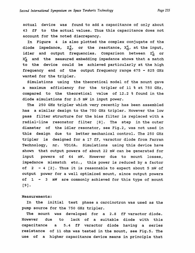
· and (iii) the idler. ... diode impedance, za, or the reactance, xa, at the input ... the...
14
Page 212 Second International Symposium on Space Terahertz Technology MULTIPLIERS FOR THz HETERODYNE SYSTEMS B.L.A. Rydberg, B.N. Lyons and U.S. Lidholm Farran Technology Ltd. Ballincollig, Cork, Ireland Abstract: The development of a 750 GHz tripler having a measured output power and efficiency of more than 12011W and 0.8 % respectively at a frequency of 803 GHz is described. The output powers and efficiencies are the highest reported for this frequency. The development of a 250 GHz tripler to be used as a pump source for the 750 GHz tripler is also described. Introduction: Due to the development of mixers, for example SIS-mixers, at frequencies around 1 THz, the demand for solid state local oscillators has been steadily increasing. In 1988 Farran Technology was commissioned by the European Space Agency to investigate and develop solid state sources based on Schottky diode multipliers to be used as local oscillators in such receivers. One of the targets has been to develop a 750 GHz solid state source with a predicted output power of 50 UW based on two triplers pumped by an 83 GHz InP-TED oscillator. We here report on the progress and results in developing such a source. Theoretical study and mount design: Using a large signal multiplier analysis program based on the principle of harmonic balance developed by Siegel et al. (1], different Schottky varactor diodes were investigated for the two multipliers. The output power for four different devices ranging from C j (0)=1.6 to 3.4 fF was calculated for the 750 GHz tripler, see Fig.l. The input power in the investigation was varied between 1-6 mW since this was assumed to be a reasonable estimate of what it is possible to achieve from a 250 GHz tripier. The description of the devices used in the simulation was simplified in that a
Transcript of · and (iii) the idler. ... diode impedance, za, or the reactance, xa, at the input ... the...

Page 212 Second International Symposium on Space Terahertz Technology
MULTIPLIERS FOR THz HETERODYNE SYSTEMSB.L.A. Rydberg, B.N. Lyons and U.S. Lidholm
Farran Technology Ltd.Ballincollig, Cork, Ireland
Abstract:The development of a 750 GHz tripler having a measured
output power and efficiency of more than 12011W and 0.8 %respectively at a frequency of 803 GHz is described. Theoutput powers and efficiencies are the highest reported forthis frequency. The development of a 250 GHz tripler to beused as a pump source for the 750 GHz tripler is alsodescribed.
Introduction:Due to the development of mixers, for example SIS-mixers,
at frequencies around 1 THz, the demand for solid statelocal oscillators has been steadily increasing. In 1988Farran Technology was commissioned by the European SpaceAgency to investigate and develop solid state sources basedon Schottky diode multipliers to be used as localoscillators in such receivers. One of the targets has beento develop a 750 GHz solid state source with a predictedoutput power of 50 UW based on two triplers pumped by an 83GHz InP-TED oscillator. We here report on the progress andresults in developing such a source.
Theoretical study and mount design:Using a large signal multiplier analysis program based on
the principle of harmonic balance developed by Siegel et al.(1], different Schottky varactor diodes were investigatedfor the two multipliers. The output power for four different
devices ranging from C j (0)=1.6 to 3.4 fF was calculated
for the 750 GHz tripler, see Fig.l. The input power in the
investigation was varied between 1-6 mW since this was
assumed to be a reasonable estimate of what it is possible
to achieve from a 250 GHz tripier. The description of the
devices used in the simulation was simplified in that a

Second International Symposium on Space Terahertz Technology Page 213
fixed layer thickness and doping of 0.49 um and91016
cm -3
respectively was used for the low doped
epitaxial region. The breakdown voltage Vb varied between
4 - 7 V for the devices, see Fig.?. The series resistance
was set to 20 ohm, which is assumed to be a reasonable value
for diodes having a capacitance 9(0) of 1.6 - 3.4 fF.The marked region in Fig.1 shows the operating condition
when the maximum voltage Vmax that is the bias voltage
plus the peak rf-voltage is approximately equal to the
breakdown voltage. Thus diodes with a capacitance between
2.2 - 2.8 fF should be the most suitable ones. The device
capacitance was chosen to be 2.8 fF. The calculated output
power for such a device is about 500 u1A7 allowing 10 dB
matching and circuit losses, yields the required outputpower of >,50 uW. Experimental results have shown that twicethe pump power needed for Vmax to reach Vb can be used(2]. Therefore it should be possible to use a pump power ofapproximately 5 mW thereby increasing the output power by afactor of two
A cross sectional view of the 750 GHz tripler is shown inFig .2. The function of the idler resonator, see Fig 2, usedin the multiplier is based on the principle developed byErickson (3]. The step in the outer diameter of the coaxialresonator is incorporated in order to achieve a better shortcircuit at the end of the idler [4]. The input waveguide isa reduced height WR-3 waveguide. The wide dimension of theoutput waveguide is 0.258 mm, thus being cutoff at 581 GHz.A conical horn was used for the output port due to the easewith which it could be machined. By proper selection of thelength and horn opening it is possible to have a nearlyidentical beam pattern in the E and H planes (5). Thewaveguide is matched to the horn using a 5X long taper witha square cross section at the horn throat, having the samecutoff frequency as the circular horn throat. Thus theimpedance discontinuity between the horn and the waveguidebecomes very small.
A scaled model of the mount (scaling factor = 83.31) wasdesigned in order to investigate and optimize the embedding

Page 214 Second International Symposium on Space Terahertz Technology
impedances seen at the input, idler and output frequenciesby the diode. Using the scaled model it was found that mostresonances in the embedding impedance were due to higherorder mode excitation in the rf-filter, see Fig.3. Theseresonances were particularly strong close to the cutofffrequency for the particular mode. Due to mechanicallimitations it was not possible to shift the coaxialTEll-mode cutoff frequencies for the rf-filter above thehighest operating frequency except for the last rf-filter
section. The TEll-mode cutoff frequencies for the other
filter sections were instead shifted to the frequency region
between the input and the idler frequency, thereby
minimizing the influence of the resonances related to the
cutoff frequency. The rf-filter is extended by a A/2 coaxial
section in order to make the middle block easier to machine,
see Fig.2.
A theoretical model was developed for the mount, where the
coupling between the rf-filter and the input waveguide was
calculated using the theory by Williamson [7]. For the
output port a simplified theoretical model was used based on
the assumption that the embedding impedance seen by the
diode is the sum of the impedances from (i) the outputwaveguide in parallel with the backshort, (ii) the rf-filter
and (iii) the idler. Though this simplified model is notsufficient to fully describe the outptit port it was used in
the absence of a more accurate one. The bias filter was
assumed to present a short circuit at the input frequency.
Using the theoretical and the scaled models of the mountthe embedding impedances seen by the device at the input,idler and output frequencies were calculated and measuredrespectively, see Fig.4. The bias filter was short circuited
in the measurements.
It can be seen in Fig.4 that there is a difference inreactance between the measurements and the calculated
values. The discrepancy in reactances is believed to be
related to the sinplifications in the theoretical model used
in the calculations. The increased capacitance due to the
measurement cable waveguide junction compared to the
Second International Symposium on Space Terahertz Technology Page 215
actual device was found to add a capacitance of only about
43 fF to the actual values. Thus this capacitance does not
account for the noted discrepancy.
In Figure 4 is also plotted the complex conjugate of the
diode impedance, za, or the reactance, xa, at the inputidler and output frequencies. Comparison between Z. >
ci, orxa and the measured embedding impedance shows that a matchto the device could be achieved particularly at the high
frequency end of the output frequency range 675 - 825 GHzwanted for the tripler.
Simulations using the theoretical model of the mount gave
a maximum efficiency for the tripler of 11 % at 750 GHz,compared to the theoretical value of 12.2 % found in thediode simulations for 2.5 mW in input power.The 250 GHz tripler which very recently has been assembled
has a similar design to the 750 GHz tripler. However the low
pass filter structure for the bias filter is replaced with a
radial-line resonator filter [8]. The step in the outer
diameter of the idler resonator, see Fig.2, was not used in
this design due to better mechanical control. The 250 GHz
tripler is designed for a 17 fF, varactor diode from Farran
Technology, nr. VD10A. Simulations using this device have
shown that output powers of about 22 mW can be generated for
input powers of 64 mW. However due to mount losses,
impedance mismatch etc., this power is reduced by a factor
of 2 - 4 [2]. Thus it is reasonable to expect about 5 mW of
output power for a well optimized mount, since output powers
of 1 - 3 mW are commonly achieved for this type of mount
(9)-
Measurements:In the initial test phase a carcinotron was used as the
pump source for the 750 GHz tripler.
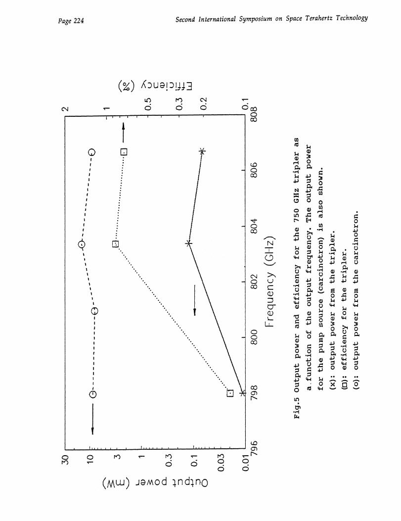
The mount was developed for a 2.8 fF varactor diode.However due to lack of a suitable diode with thiscapacitance a 5.4 fF varactor diode having a series
resistance of 11 ohm was tested in the mount, see Fig.5. The
use of a higher capacitance device means in principle that

Page 216. Second International Symposium on Space Terahertz Technology
more pump power is needed in order to achieve the same
output power as for a 2.8 fF device, assuming the same
series resistance for the diodes. However this is
compensated for by the much smaller series resistance for
the 5.4 fF, 11 ohm as compared to 20 ohm assumed for the 2.8
fF device.Computer simulations of the tripler using the theoretical
model showed that it is possible to match the 5.4 fF diode,
by reducing the whisker length to 50 um compared to 60 um
for the 2.8 fF device, though with a loss in maximum
efficiency. Thus it was found using computer simulations
that a maximum efficiency of 12.8 % for the mount compared
to a maximum of 16.3 % using optimum embedding impedancescould be achieved at 750 GHz, at 6 mW input power. This canbe compared to an efficiency of 18.4 % for the 2.8 fF diodeat optimum embedding impedances using the same input power.The small difference, that is 16.3 - 18.4 % is mainly due tothe difference in cutoff frequency for the devices.
The measured results for the 750 GHz tripler using the 5.4fF diode are shown in Fig.5. The output power and efficiencyare as can be seen in Fig.5, very sensitive to the inputpower. The higher input power means that a larger backbiasvoltage or in this case a smaller forward bias voltage canbe used thereby making the diodes work more in varactormode, see Fig.6. Thus the output power and efficiency usingthis operating point are greater, compare Fig.5 and 6. Itcan be seen, comparing Fig.6 with Fig.5, that the operatingpoints vary according to the pump power available from thecarcinotron and seem to be less dependent on the pumpfrequency Thus the passband for the rf-filter seems to havelittle variation in attenuation over the investigatedfrequency range, which was also anticipated.
The work on optimizing the 250 GHz tripler is about tocommence. Initial output powers of 1 mW at 250 GHz has beenachieved.

Second International Symposium on Space Terahertz Technology Page 217
Future work:The 250 GHz tripler will be optimized as a pump source for
the 750 GHz tripler.The 5.4 fF varactor will be replaced by a 2.8 fF device
which we have now fabricated, having a series resistance of16 ohm.
Single barrier varactors (SBV) will be tested in themount. Due to the symmetrical I-V and C-V characteristic ofthe SBV-diodes only odd harmonic are generated in thesedevices [10]. Thus they are particularly suitable for use inexample triplers since no idler resonator is needed, therebyreducing the losses at the idler frequency to zero [11].
Conclusions:The design and development of a solid state source for 750
GHz consisting of two triplers has been described. State of
the art output powers of more than 120 uW has been achieved
at 803 GHz using a carcinotron as the initial test source
for the 750 GHz tripler.
Acknowledgements:
We would like to thank Dr. D. Vizard for helpfu11discussions and Mr. J. Pike for assistance in selecting thediodes and diode manufacture. Messrs. K. Barrett and M.
Fehilly are thanked for skilful manufacturing and assemblyof the multipliers as well as technical ideas. Miss M.Tubridy is also thanked for help with optimization of themount using Touchstone.
The European Space Agency (ESA) is acknowledged forfinancial support (ESA contract no. 7898/88/NL/PB).

Page 218 Second International Symposium on Space Terahertz Technology
References:
1. P.H. Siegel, A.R. Kerr and W. Hwang, Topics in the
optimization of millimeter-wave mixers," NASA tech.
paper 2287, 1984.
2. N.R. Erickson, "Very high efficiency frequency triplerfor 100-300 GHz," Proc. of the 10th Int. Conf. on
Infrared and Millimeter Waves, pp. 54-55, 1985.
3. N.R. Erickson, "A high efficiency frequency tripler for230 GHz," Proc. of the 12'th European Microwave Conf.,
pp. 241-246, 1982.
4. N.R. Erickson, "High efficiency submillimeter frequencymultipliers," Proc. of IEEE-MTT Conf. 1990, pp.
1301-1304, 1990.
5. R.C. Johnson and H. Janik, Antenna engineering
handbook, second edition, McGraw-Hill, pp. 15-13 -15-17, 1984.
6. T.J. Tolmunen and A.V. Raisanen, "An efficient
Schottky-varactor frequency multiplier at millimeter
waves, Part II: Tripler," Int. Journal of Infrared and
Millimeter Waves, vol. 8, pp. 1337-1353, 1987.
7. A.G. Williamson, "Analysis and modelling of "two-gap"
coaxial-line rectangular waveguide junctions," IEEE
Trans. on Microwave Theory and Tech., vol. MTT-31, pp.
295-302, 1983.
8. A. Rydberg, "Calculation of microwave radial-line
filters," Microwave and Optical Technology Lett.,
vol.1 pp. 4-7, 1988.
9. A. Rydberg, "Oscillator and multiplier development for
millimeterwave radioastronomy," Proceedings of the
workshop on solid state sources at millimeter and
subminimeter wavelengths Ulm BRD, October 1987.

Second International Symposium on Space Terahertz Technology Page 219
10. E. Kollberg and A. Rydberg, "Quantum-barrier-varactor
diodes for high-efficiency millimeter-wavemultipliers," Electron. Lett., vol. 25, pp. 1696-1698,
1989.
11. A. Rydberg, H. Gronqvist and E. Kollberg, "Millimeter-
and submillimeter-wave multipliers using
Quantum-Barrier-Varactor (QBV) diodes," IEEE ElectronDevice Lett., vol. 11, pp. 373-375, 1990.

53
4
Inp
ut
po
wer
(m
W)
1
4.5
5.9 &
2.6 1,9
1.6
D.5
.6
3.8
4.9
8.2
8.?.
..
--
7.8
7.0
.68.
6
7.1
6.1
3.9
3.5
5.0
Fig
.1 C
alcu
late
d ou
tput
pow
er a
s a
func
tion
of
inpu
t po
wer
for
Sch
ottk
y va
ract
or d
iode
s ha
ving
a c
apac
itan
ce9(0
) of
bet
wee
n 1
.6 -
3.4
fF
. T
he
bia
s volt
age
isop
tim
ized
for
bes
t ef
fici
ency
. The
num
bers
alo
ng t
hecu
rves
are
the
max
imum
vol
tage
s V
max
acr
oss
the
dev
ice
at t
he
par
ticu
lar
op
erat
ing
po
int.
(A):
9(0
) is
1.6
f F, V
b =
4 V
.(1
3): C
j (0)
is 2
.2f
F, V
b =
6 V
.(0
): C
i (0)
is 2
.8f
F, V
b =
6.5
V.
(x):
Ci (
0) is
3.4
fF, V
b =
7 V
.

UPPERBLOCK
FILTERBIAS
•■■•■••••
A/2RF-FILTER
MIDDLEBLOCK
BRASSMACOR
SLID1NGFIT
A
LOWERBLOCK
52
IDLERRESONATOR
Second International Symposium on Space Terahertz Technology Page 221
Fig.2 Cross — sectional view of the 750 GHz triplex'. (Not toscale). B1= 0.091 mm, B2=0.041 ram, LH=2X, DH=2.54A,LT=5A.

8.5
966
775
0
I
OU
TPU
T RAN
GE)
,
7.5
4.5
1.2
55.
56
6.5
417
500
IDLE
R R
AN
GE
I >1
7 583
Fig
.3 M
easu
red
reso
nanc
es a
nd c
alcu
late
d co
axia
l TE
ll-m
ode
cuto
ff f
req
uen
cies
fo
r th
e rf
-fil
ter
as a
fu
nct
ion
of
freq
uenc
y. T
he m
easu
red
reso
nanc
es a
re p
lott
ed a
s th
edi
amet
er o
f th
e re
sona
nce
loop
"M
", s
ee s
ketc
h in
Fig
.3. T
he m
axim
um v
alue
of
"M"
is 1
. The
fre
quen
cy is
plot
ted
both
as
the
real
and
the
sca
led
mod
elfr
eque
ncie
s fo
r th
e m
ulti
plie
r. D
=0.
25 m
m,
(1 1=0
.13
ram
, d2=0
.19
mm
, d3=0
.1 m
m.

.2 .5 i 2
Second International Symposium on Space Terahertz Technology Page 223
Fig.4 Measured and calculated embedding impedances seen bythe diode at the input, idler and output frequencies.Zx
d and X are the complex conjugate of the diodeimpedance and reactance respectively at 250, 500 or750 GHz. M is measured and C is calculated in thefigures, except for the idler where "o" = calculatedand "x" is measured.A: input frequency, 250 GHz.B: idler frequencies, 450, 500 and 550 GHz.C: output frequency, 750 GHz.
(1.)
0.01
796
30 3
0.2
cez- 8* c.n0.
180
8
tr)
"tt ;21
Fig
.5 O
utpu
t po
wer
and
eff
icie
ncy
for
the
750
GH
z tr
iple
r as
a. f
unct
ion
of t
he o
utpu
t fr
eque
ncy.
The
out
put
pow
erfo
r th
e pu
mp
sour
ce (
carc
inot
ron)
is
also
sho
wn.
(x):
out
put
pow
er f
rom
the
tri
pler
.(0
): e
ffic
iency
for
the
trip
ler.
(o):
out
put
pow
er f
rom
the
car
cino
tron
.
0.3
Cl_
0.03
798
800
802
804
806
Freq
uenc
y (0
I-1z)
1 0.5
0.3
(t)
Ld4-
;4.

I-V
803
1
-0
0.01
0.00
3
807
798
D
0.00
10
0.1
0.2
0.3
0.4
0.5
0.6
0.7
0.8
0.9
1
Bia
s vo
ltage
(V)
Fig
.6 I
-V c
urve
and
ope
rati
ng p
oint
s fo
r th
e 5.
4 fF
dio
de.
Th
e n
um
ber
s at
the
oper
atin
g p
oin
ts r
efer
to t
he
oper
atin
g fr
eque
ncy
in W
iz f
or t
he p
arti
cula
rop
erat
ing
poin
t.