· Altera Corporation iii Preliminary Contents Chapter Revision Dates...
468
Preliminary Information 101 Innovation Drive San Jose, CA 95134 (408) 544-7000 http://www.altera.com Cyclone Device Handbook, Volume 1 C5V1-1.0
-
Upload
vuongkhuong -
Category
Documents
-
view
216 -
download
0
Transcript of · Altera Corporation iii Preliminary Contents Chapter Revision Dates...
Preliminary Information101 Innovation DriveSan Jose, CA 95134(408) 544-7000http://www.altera.com
Cyclone Device Handbook, Volume 1
C5V1-1.0

Copyright © 2003 Altera Corporation. All rights reserved. Altera, The Programmable Solutions Company, the stylized Altera logo, specific device des-ignations, and all other words and logos that are identified as trademarks and/or service marks are, unless noted otherwise, the trademarks andservice marks of Altera Corporation in the U.S. and other countries. All other product or service names are the property of their respective holders. Al-tera products are protected under numerous U.S. and foreign patents and pending applications, maskwork rights, and copyrights. Altera warrantsperformance of its semiconductor products to current specifications in accordance with Altera's standard warranty, but reserves the right to makechanges to any products and services at any time without notice. Altera assumes no responsibility or liability arising out of the ap-plication or use of any information, product, or service described herein except as expressly agreed to in writing by AlteraCorporation. Altera customers are advised to obtain the latest version of device specifications before relying on any published in-formation and before placing orders for products or services.
Printed on recycled paper
ii Altera CorporationPreliminary

Altera Corporation iiiPreliminary
Contents
Chapter Revision Dates ........................................................................... xi
About this Handbook ............................................................................. xiiiHow to Find Information ..................................................................................................................... xiiiHow to Contact Altera .......................................................................................................................... xiiiTypographic Conventions .................................................................................................................... xiv
Section I. Cyclone FPGA Family Data SheetRevision History ....................................................................................................................... Section I–1
Chapter 1. IntroductionIntroduction ............................................................................................................................................ 1–1Features ................................................................................................................................................... 1–2
Chapter 2. Cyclone ArchitectureFunctional Description .......................................................................................................................... 2–1Logic Array Blocks ................................................................................................................................ 2–3
LAB Interconnects ............................................................................................................................ 2–3LAB Control Signals ......................................................................................................................... 2–4
Logic Elements ....................................................................................................................................... 2–5LUT Chain & Register Chain .......................................................................................................... 2–7addnsub Signal ................................................................................................................................. 2–7LE Operating Modes ........................................................................................................................ 2–7
MultiTrack Interconnect ..................................................................................................................... 2–12Embedded Memory ............................................................................................................................. 2–18
Memory Modes ............................................................................................................................... 2–18Parity Bit Support ........................................................................................................................... 2–20Shift Register Support .................................................................................................................... 2–20Memory Configuration Sizes ........................................................................................................ 2–21Byte Enables .................................................................................................................................... 2–23Control Signals & M4K Interface ................................................................................................. 2–23Independent Clock Mode .............................................................................................................. 2–25Input/Output Clock Mode ........................................................................................................... 2–25Read/Write Clock Mode ............................................................................................................... 2–27Single-Port Mode ............................................................................................................................ 2–28
Global Clock Network & Phase-Locked Loops ............................................................................... 2–29Global Clock Network ................................................................................................................... 2–29Dual-Purpose Clock Pins .............................................................................................................. 2–30

1–iv Altera CorporationPreliminary
Cyclone Device Handbook, Volume 1
Combined Resources ..................................................................................................................... 2–31PLLs .................................................................................................................................................. 2–32Clock Multiplication & Division .................................................................................................. 2–35External Clock Inputs .................................................................................................................... 2–36External Clock Outputs ................................................................................................................. 2–36Clock Feedback ............................................................................................................................... 2–37Phase Shifting ................................................................................................................................. 2–37Lock Detect Signal .......................................................................................................................... 2–37Programmable Duty Cycle ........................................................................................................... 2–38Control Signals ................................................................................................................................ 2–38
I/O Structure ........................................................................................................................................ 2–39External RAM Interfacing ............................................................................................................. 2–46DDR SDRAM & FCRAM .............................................................................................................. 2–46Programmable Drive Strength ..................................................................................................... 2–49Open-Drain Output ........................................................................................................................ 2–50Slew-Rate Control .......................................................................................................................... 2–50Bus Hold .......................................................................................................................................... 2–51Programmable Pull-Up Resistor .................................................................................................. 2–51Advanced I/O Standard Support ................................................................................................ 2–52LVDS I/O Pins ................................................................................................................................ 2–54MultiVolt I/O Interface ................................................................................................................. 2–54
Power Sequencing & Hot Socketing ................................................................................................. 2–55
Chapter 3. Configuration & TestingIEEE Std. 1149.1 (JTAG) Boundary Scan Support ............................................................................. 3–1SignalTap II Embedded Logic Analyzer ............................................................................................ 3–5Configuration ......................................................................................................................................... 3–5
Operating Modes .............................................................................................................................. 3–6Configuration Schemes ................................................................................................................... 3–6
Chapter 4. DC & Switching CharacteristicsOperating Conditions ........................................................................................................................... 4–1Power Consumption ............................................................................................................................. 4–8Timing Model ......................................................................................................................................... 4–9
Preliminary & Final Timing ............................................................................................................ 4–9Internal Timing Parameters .......................................................................................................... 4–10External Timing Parameters ......................................................................................................... 4–14External I/O Delay Parameters .................................................................................................... 4–21Maximum Input & Output Clock Rates ...................................................................................... 4–27
Chapter 5. Reference & Ordering InformationSoftware .................................................................................................................................................. 5–1Device Pin-Outs ..................................................................................................................................... 5–1Ordering Information ........................................................................................................................... 5–1

Altera Corporation 1–vPreliminary
Contents
Section II. Clock ManagementRevision History ..................................................................................................................... Section II–1
Chapter 6. Using PLLs in Cyclone DevicesIntroduction ............................................................................................................................................ 6–1
Hardware Overview ........................................................................................................................ 6–1Software Overview .......................................................................................................................... 6–4Pins & Clock Network Connections .............................................................................................. 6–6
Hardware Features ................................................................................................................................ 6–8Clock Multiplication & Division .................................................................................................... 6–8Phase Shifting ................................................................................................................................... 6–9Programmable Duty Cycle ........................................................................................................... 6–10External Clock Output ................................................................................................................... 6–11Control Signals ................................................................................................................................ 6–12
Clock Feedback Modes ....................................................................................................................... 6–13Normal Mode .................................................................................................................................. 6–13Zero Delay Buffer Mode ................................................................................................................ 6–14No Compensation .......................................................................................................................... 6–15
Pins ......................................................................................................................................................... 6–16Board Layout ........................................................................................................................................ 6–17
VCCA & GNDA ............................................................................................................................. 6–17Jitter Considerations ...................................................................................................................... 6–19
Specifications ........................................................................................................................................ 6–20Software Support ................................................................................................................................. 6–21
Quartus II altpll Megafunction ..................................................................................................... 6–21altpll Input Ports ............................................................................................................................. 6–22altpll Output Ports ......................................................................................................................... 6–23MegaWizard Customization ......................................................................................................... 6–23MegaWizard Page Description ..................................................................................................... 6–25Compilation Report ....................................................................................................................... 6–31Timing Analysis .............................................................................................................................. 6–33Simulation ....................................................................................................................................... 6–37
Global Clock Network ........................................................................................................................ 6–38Dedicated Clock Input Pins .......................................................................................................... 6–40Dual-Purpose Clock I/O Pins ...................................................................................................... 6–40Combined Sources .......................................................................................................................... 6–41
Conclusion ............................................................................................................................................ 6–43
Section III. MemoryRevision History .................................................................................................................... Section III–1
Chapter 7. On-Chip Memory Implementations Using Cyclone Memory BlocksIntroduction ............................................................................................................................................ 7–1M4K Memory Features ......................................................................................................................... 7–1
1–vi Altera CorporationPreliminary
Cyclone Device Handbook, Volume 1
Parity Bit Support ............................................................................................................................. 7–2Byte-Enable Support ........................................................................................................................ 7–3Power-up Conditions & Memory Initialization ........................................................................... 7–4
Using M4K Memory .............................................................................................................................. 7–4Implementing Single-Port Mode .................................................................................................... 7–5Implementing Simple Dual-Port Mode ......................................................................................... 7–6Implementing True Dual-Port Mode ............................................................................................ 7–8Implementing Shift-Register Mode ............................................................................................. 7–11Implementing ROM Mode ............................................................................................................ 7–12Implementing FIFO Buffers .......................................................................................................... 7–12
Clock Modes ......................................................................................................................................... 7–13Independent Clock Mode .............................................................................................................. 7–13Input/Output Clock Mode ........................................................................................................... 7–15Read/Write Clock Mode ............................................................................................................... 7–17Single-Port Mode ............................................................................................................................ 7–18
Synchronous & Pseudo-Asynchronous Modes ............................................................................... 7–19Read-during-Write Operation at the Same Address ...................................................................... 7–20
Same-Port Read-during-Write Mode .......................................................................................... 7–20Mixed-Port Read-during-Write Mode ........................................................................................ 7–21
Conclusion ............................................................................................................................................ 7–23
Section IV. I/O StandardsRevision History .................................................................................................................... Section IV–1
Chapter 8. Using Selectable I/O Standards in Cyclone DevicesIntroduction ............................................................................................................................................ 8–1Supported I/O Standards ..................................................................................................................... 8–2
3.3-V LVTTL (EIA/JEDEC Standard JESD8-B) ............................................................................ 8–23.3-V LVCMOS (EIA/JEDEC Standard JESD8-B) ....................................................................... 8–32.5-V LVTTL Normal & Wide Voltage Ranges (EIA/JEDEC Standard EIA/JESD8-5) ......... 8–32.5-V LVCMOS Normal & Wide Voltage Ranges (EIA/JEDEC Standard EIA/JESD8-5) .... 8–41.8-V LVTTL Normal & Wide Voltage Ranges (EIA/JEDEC Standard EIA/JESD8-7) ......... 8–41.8-V LVCMOS Normal & Wide Voltage Ranges (EIA/JEDEC Standard EIA/JESD8-7) .... 8–41.5-V LVCMOS Normal & Wide Voltage Ranges (EIA/JEDEC Standard JESD8-11) ............ 8–53.3-V (PCI Special Interest Group (SIG) PCI Local Bus Specification Revision 2.2) ............... 8–5SSTL-3 Class I & II (EIA/JEDEC Standard JESD8-8) .................................................................. 8–5SSTL-2 Class I & II (EIA/JEDEC Standard JESD8-9A) ............................................................... 8–6LVDS (ANSI/TIA/EIA Standard ANSI/TIA/EIA-644) ............................................................ 8–7Differential SSTL-2 - EIA/JEDEC Standard JESD8-9A ............................................................... 8–8
Cyclone I/O Banks ................................................................................................................................ 8–8Programmable Current Drive Strength ............................................................................................ 8–11Hot Socketing ....................................................................................................................................... 8–12I/O Termination .................................................................................................................................. 8–12
Voltage-Referenced I/O Standard Termination ........................................................................ 8–13Differential I/O Standard Termination ...................................................................................... 8–13
Altera Corporation 1–viiPreliminary
Contents
Pad Placement & DC Guidelines ....................................................................................................... 8–13Differential Pad Placement Guidelines ....................................................................................... 8–13VREF Pad Placement Guidelines ................................................................................................... 8–13DC Guidelines ................................................................................................................................. 8–16
Quartus II Software Support .............................................................................................................. 8–17Compiler Settings ........................................................................................................................... 8–17
Conclusion ............................................................................................................................................ 8–20More Information ................................................................................................................................ 8–21References ............................................................................................................................................. 8–21
Chapter 9. Implementing LVDS in Cyclone DevicesIntroduction ............................................................................................................................................ 9–1Cyclone LVDS I/O Banks ..................................................................................................................... 9–1Cyclone LVDS I/O Interface ................................................................................................................ 9–3
Clock Domains .................................................................................................................................. 9–3LVDS Receiver & Transmitter ........................................................................................................ 9–4LVDS Timing in Cyclone Devices .................................................................................................. 9–7
Cyclone Receiver & Transmitter Termination ................................................................................... 9–8Implementing Cyclone LVDS I/O Pins in the Quartus II Software ............................................ 9–10
Transmitting Serial Data on Cyclone LVDS Outputs ............................................................... 9–10Capturing Serial Data on Cyclone LVDS Inputs ....................................................................... 9–14
Design Guidelines ............................................................................................................................... 9–16Differential Pad Placement Guidelines ....................................................................................... 9–17Board Design Considerations ....................................................................................................... 9–17
Conclusion ............................................................................................................................................ 9–18
Section V. Design ConsiderationsRevision History ..................................................................................................................... Section V–1
Chapter 10. Implementing Double Data Rate I/O Signaling in Cyclone DevicesIntroduction .......................................................................................................................................... 10–1Double Data Rate Input ...................................................................................................................... 10–1Double Data Rate Output ................................................................................................................... 10–2Bidirectional Double Data Rate ......................................................................................................... 10–3DDR Memory Support ........................................................................................................................ 10–4Conclusion ............................................................................................................................................ 10–4
Chapter 11. Using Cyclone Devices in Multiple-Voltage SystemsIntroduction .......................................................................................................................................... 11–1I/O Standards ...................................................................................................................................... 11–1MultiVolt I/O Operation .................................................................................................................... 11–25.0-V Device Compatibility ................................................................................................................ 11–3Hot-Socketing ....................................................................................................................................... 11–6
Devices Can Be Driven before Power-Up ................................................................................... 11–6I/O Pins Remain Tri-Stated during Power-Up .......................................................................... 11–6

1–viii Altera CorporationPreliminary
Cyclone Device Handbook, Volume 1
Signal Pins Do Not Drive the VCCIO or VCCINT Power Supplies .............................................. 11–6Power-Up Sequence ............................................................................................................................ 11–7Power-On Reset ................................................................................................................................... 11–7Conclusion ............................................................................................................................................ 11–8
Chapter 12. Designing with 1.5-V DevicesIntroduction .......................................................................................................................................... 12–1Power Sequencing & Hot Socketing ................................................................................................. 12–1Using MultiVolt I/O Pins ................................................................................................................... 12–2Voltage Regulators .............................................................................................................................. 12–3
Linear Voltage Regulators ............................................................................................................. 12–4Switching Voltage Regulators ...................................................................................................... 12–6Maximum Output Current ........................................................................................................... 12–8Selecting Voltage Regulators ........................................................................................................ 12–8Voltage Divider Network ............................................................................................................ 12–101.5-V Regulator Circuits .............................................................................................................. 12–10
1.5-V Regulator Application Examples .......................................................................................... 12–19Synchronous Switching Regulator Example ............................................................................ 12–20
Board Layout ...................................................................................................................................... 12–21Split-Plane Method ....................................................................................................................... 12–23
Conclusion .......................................................................................................................................... 12–23References ........................................................................................................................................... 12–24
Section VI. ConfigurationRevision History .................................................................................................................... Section VI–1
Chapter 13. Configuring Cyclone FPGAsIntroduction .......................................................................................................................................... 13–1Device Configuration Overview ....................................................................................................... 13–1Data Compression ............................................................................................................................... 13–3Configuration Schemes ....................................................................................................................... 13–6
Active Serial Configuration (Serial Configuration Devices) .................................................... 13–7Passive Serial Configuration ....................................................................................................... 13–13JTAG-Based Configuration ......................................................................................................... 13–25
Combining Configuration Schemes ................................................................................................ 13–39Active Serial & JTAG ................................................................................................................... 13–39Passive Serial & JTAG .................................................................................................................. 13–40
Device Options ................................................................................................................................... 13–41Device Configuration Pins ............................................................................................................... 13–45Device Configuration Files ............................................................................................................... 13–47
SRAM Object File (.sof) ............................................................................................................... 13–47Programmer Object File (.pof) .................................................................................................... 13–48Raw Binary File (.rbf) ................................................................................................................... 13–48Hexadecimal (Intel-Format) File (.hex) ..................................................................................... 13–48Tabular Text File (.ttf) .................................................................................................................. 13–48

Altera Corporation 1–ixPreliminary
Contents
Jam File (.jam) ............................................................................................................................... 13–49Jam Byte-Code File (.jbc) ............................................................................................................. 13–49
Configuration Reliability .................................................................................................................. 13–49Board Layout Tips ............................................................................................................................. 13–50
Chapter 14. Serial Configuration Devices (EPCS1 & EPCS4) Data SheetFeatures ................................................................................................................................................. 14–1Functional Description ........................................................................................................................ 14–2Accessing Memory in Serial Configuration Devices ...................................................................... 14–3Pin Description ..................................................................................................................................... 14–4Programming & Configuration File Support .................................................................................. 14–4Cyclone FPGA Configuration ............................................................................................................ 14–7Power & Operation ............................................................................................................................ 14–11
Power Mode .................................................................................................................................. 14–11Power-On Reset ............................................................................................................................ 14–11Error Detection ............................................................................................................................. 14–11
Operating Conditions ....................................................................................................................... 14–12Package ................................................................................................................................................ 14–13Ordering Code ................................................................................................................................... 14–14
Index

1–x Altera CorporationPreliminary
Cyclone Device Handbook, Volume 1

Altera Corporation xiPreliminary
Chapter Revision Dates
The chapters in this book, Cyclone Device Handbook, Volume 1, were revised on the following dates. Where chapters or groups of chapters are available separately, part numbers are listed.
Chapter 1. IntroductionRevised: May 2003Part number: C51001-1.0
Chapter 2. Cyclone ArchitectureRevised: May 2003Part number: C51002-1.0
Chapter 3. Configuration & TestingRevised: May 2003Part number: C51003-1.0
Chapter 4. DC & Switching CharacteristicsRevised: May 2003Part number: C51004-1.0
Chapter 5. Reference & Ordering InformationRevised: May 2003Part number: C51005-1.0
Chapter 6. Using PLLs in Cyclone DevicesRevised: May 2003Part number: C51006-1.0
Chapter 7. On-Chip Memory Implementations Using Cyclone Memory BlocksRevised: May 2003Part number: C51007-1.0
Chapter 8. Using Selectable I/O Standards in Cyclone DevicesRevised: May 2003Part number: C51008-1.0
Chapter 9. Implementing LVDS in Cyclone DevicesRevised: May 2003Part number: C51009-1.0

1–xii Altera CorporationPreliminary
Cyclone Device Handbook, Volume 1
Chapter 10. Implementing Double Data Rate I/O Signaling in Cyclone DevicesRevised: May 2003Part number: C51010-1.0
Chapter 11. Using Cyclone Devices in Multiple-Voltage SystemsRevised: May 2003Part number: C51011-1.0
Chapter 12. Designing with 1.5-V DevicesRevised: May 2003Part number: C51012-1.0
Chapter 13. Configuring Cyclone FPGAsRevised: May 2003Part number: C51013-1.0
Chapter 14. Serial Configuration Devices (EPCS1 & EPCS4) Data SheetRevised: May 2003Part number: C51014-1.0

Altera Corporation xiiiPreliminary
About this Handbook
This handbook provides comprehensive information about the Altera® Cyclone™ family of devices.
How to Find Information
You can find more information in the following ways:
The Adobe Acrobat Find feature, which searches the text of a PDF document. Click the binoculars toolbar icon to open the Find dialog box.
Acrobat bookmarks, which serve as an additional table of contents in PDF documents.
Thumbnail icons, which provide miniature previews of each page, provide a link to the pages.
Numerous links, shown in green text, which allow you to jump to related information.
How to Contact Altera
For the most up-to-date information about Altera products, go to the Altera world-wide web site at www.altera.com. For technical support on this product, go to www.altera.com/mysupport. For additional information about Altera products, consult the sources shown below.
Information Type USA & Canada All Other Locations
Technical support www.altera.com/mysupport/ www.altera.com/mysupport/
(800) 800-EPLD (3753)(7:00 a.m. to 5:00 p.m. Pacific Time)
(408) 544-7000 (1)(7:00 a.m. to 5:00 p.m. Pacific Time)
Product literature www.altera.com www.altera.com
Altera literature services [email protected] (1) [email protected] (1)
Non-technical customer service
(800) 767-3753 (408) 544-7000 (7:30 a.m. to 5:30 p.m. Pacific Time)
FTP site ftp.altera.com ftp.altera.com
Note to table:(1) You can also contact your local Altera sales office or sales representative.

1–xiv Altera CorporationPreliminary
Cyclone Device Handbook, Volume 1
Typographic Conventions
This document uses the typographic conventions shown below.
Visual Cue Meaning
Bold Type with Initial Capital Letters
Command names, dialog box titles, checkbox options, and dialog box options are shown in bold, initial capital letters. Example: Save As dialog box.
bold type External timing parameters, directory names, project names, disk drive names, filenames, filename extensions, and software utility names are shown in bold type. Examples: fMAX, \qdesigns directory, d: drive, chiptrip.gdf file.
Italic Type with Initial Capital Letters
Document titles are shown in italic type with initial capital letters. Example: AN 75: High-Speed Board Design.
Italic type Internal timing parameters and variables are shown in italic type. Examples: tPIA, n + 1.
Variable names are enclosed in angle brackets (< >) and shown in italic type. Example: <file name>, <project name>.pof file.
Initial Capital Letters Keyboard keys and menu names are shown with initial capital letters. Examples: Delete key, the Options menu.
“Subheading Title” References to sections within a document and titles of on-line help topics are shown in quotation marks. Example: “Typographic Conventions.”
Courier type Signal and port names are shown in lowercase Courier type. Examples: data1, tdi, input. Active-low signals are denoted by suffix n, e.g., resetn.
Anything that must be typed exactly as it appears is shown in Courier type. For example: c:\qdesigns\tutorial\chiptrip.gdf. Also, sections of an actual file, such as a Report File, references to parts of files (e.g., the AHDL keyword SUBDESIGN), as well as logic function names (e.g., TRI) are shown in Courier.
1., 2., 3., anda., b., c., etc.
Numbered steps are used in a list of items when the sequence of the items is important, such as the steps listed in a procedure.
• Bullets are used in a list of items when the sequence of the items is not important.
v The checkmark indicates a procedure that consists of one step only.
1 The hand points to information that requires special attention.
r The angled arrow indicates you should press the Enter key.
f The feet direct you to more information on a particular topic.

Altera Corporation Section I–1Preliminary
Section I. Cyclone FPGAFamily Data Sheet
This section provides designers with the data sheet specifications for Cyclone devices. The chapters contain feature definitions of the internal architecture, configuration and JTAG boundary-scan testing information, DC operating conditions, AC timing parameters, a reference to power consumption, and ordering information for Cyclone devices.
This section contains the following chapters:
Chapter 1. Introduction
Chapter 2. Cyclone Architecture
Chapter 3. Configuration & Testing
Chapter 4. DC & Switching Characteristics
Chapter 5. Reference & Ordering Information
Revision History The table below shows the revision history for Chapters 1 through 5.
Chapter(s) Date / Version Changes Made
1 through 5 May 2003v1.0
Added the EP1C4 device. Updated the “Timing Model” section.

Section I–2 Altera CorporationPreliminary
Cyclone FPGA Family Data Sheet Cyclone Device Handbook, Volume 1

Altera Corporation 1–1May 2003 Preliminary
1. Introduction
Introduction The CycloneTM field programmable gate array family is based on a 1.5-V, 0.13-mm, all-layer copper SRAM process, with densities up to 20,060 logic elements (LEs) and up to 288 Kbits of RAM. With features like phase-locked loops (PLLs) for clocking and a dedicated double data rate (DDR) interface to meet DDR SDRAM and fast cycle RAM (FCRAM) memory requirements, Cyclone devices are a cost-effective solution for data-path applications. Cyclone devices support various I/O standards, including LVDS at data rates up to 311 megabits per second (Mbps) and 66-MHz, 32-bit peripheral component interconnect (PCI), for interfacing with and supporting ASSP and ASIC devices. Altera also offers new low-cost serial configuration devices to configure Cyclone devices.
The following shows the main sections in the Cyclone FPGA Family Data Sheet:
Section Page
Features . . . . . . . . . . . . . . . . . . . . . . . . . . . . . . . . . . . . . . . . . . . . . 1–2
Functional Description . . . . . . . . . . . . . . . . . . . . . . . . . . . . . . . . 2–1Logic Array Blocks. . . . . . . . . . . . . . . . . . . . . . . . . . . . . . . . . . . . 2–3Logic Elements . . . . . . . . . . . . . . . . . . . . . . . . . . . . . . . . . . . . . . . 2–5MultiTrack Interconnect . . . . . . . . . . . . . . . . . . . . . . . . . . . . . . 2–12Embedded Memory. . . . . . . . . . . . . . . . . . . . . . . . . . . . . . . . . . 2–18Global Clock Network & Phase-Locked Loops. . . . . . . . . . . 2–29I/O Structure . . . . . . . . . . . . . . . . . . . . . . . . . . . . . . . . . . . . . . . 2–39Power Sequencing & Hot Socketing . . . . . . . . . . . . . . . . . . . . 2–55
IEEE Std. 1149.1 (JTAG) Boundary Scan Support . . . . . . . . . . 3–1SignalTap II Embedded Logic Analyzer . . . . . . . . . . . . . . . . . 3–5Configuration . . . . . . . . . . . . . . . . . . . . . . . . . . . . . . . . . . . . . . . . 3–5
Operating Conditions . . . . . . . . . . . . . . . . . . . . . . . . . . . . . . . . . 4–1Power Consumption . . . . . . . . . . . . . . . . . . . . . . . . . . . . . . . . . . 4–8Timing Model . . . . . . . . . . . . . . . . . . . . . . . . . . . . . . . . . . . . . . . . 4–9
Software. . . . . . . . . . . . . . . . . . . . . . . . . . . . . . . . . . . . . . . . . . . . . 5–1Device Pin-Outs . . . . . . . . . . . . . . . . . . . . . . . . . . . . . . . . . . . . . . 5–1Ordering Information . . . . . . . . . . . . . . . . . . . . . . . . . . . . . . . . . 5–1
C51001-1.0

1–2 Altera CorporationPreliminary May 2003
Cyclone Device Handbook, Volume 1
Features The Cyclone device family offers the following features:
2,910 to 20,060 LEs, see Table 1–1 Up to 294,912 RAM bits (36,864 bytes) Supports configuration through low-cost serial configuration device Support for LVTTL, LVCMOS, SSTL-2, and SSTL-3 I/O standards Support for 66-MHz, 32-bit PCI standard Low speed (311 Mbps) LVDS I/O support Up to two PLLs per device provide clock multiplication and phase
shifting Up to eight global clock lines with six clock resources available per
logic array block (LAB) row Support for external memory, including DDR SDRAM (133 MHz),
FCRAM, and single data rate (SDR) SDRAM Support for multiple intellectual property (IP) cores, including
Altera MegaCore functions and Altera Megafunctions Partners Program (AMPPSM) megafunctions.
Table 1–1. Cyclone Device Features
Feature EP1C3 EP1C4 EP1C6 EP1C12 EP1C20
LEs 2,910 4,000 5,980 12,060 20,060
M4K RAM blocks (128 × 36 bits) 13 17 20 52 64
Total RAM bits 59,904 78,336 92,160 239,616 294,912
PLLs 1 2 2 2 2
Maximum user I/O pins (1) 104 301 185 249 301
Note to Table 1–1:(1) This parameter includes global clock pins.

Altera Corporation 1–3May 2003 Preliminary
Features
Cyclone devices are available in quad flat pack (QFP) and space-saving FineLine BGA packages (see Table 1–2 through 1–3).
Table 1–2. Cyclone Package Options & I/O Pin Counts
Device 100-Pin TQFP (1)
144-Pin TQFP (1), (2)
240-Pin PQFP (1)
256-Pin FineLine BGA
324-Pin FineLine BGA
400-Pin FineLine BGA
EP1C3 65 104
EP1C4 249 301
EP1C6 98 185 185
EP1C12 173 185 249
EP1C20 233 301
Notes to Table 1–2:(1) TQFP: thin quad flat pack.
PQFP: plastic quad flat pack.(2) Cyclone devices support vertical migration within the same package (i.e., designers can migrate between the
EP1C3 device in the 144-pin TQFP package and the EP1C6 device in the same package)
Table 1–3. Cyclone QFP & FineLine BGA Package Sizes
Dimension 100-Pin TQFP
144-Pin TQFP
240-Pin PQFP
256-Pin FineLine
BGA
324-Pin FineLine
BGA
400-Pin FineLine
BGA
Pitch (mm) 0.5 0.5 0.5 1.0 1.0 1.0
Area (mm2) 256 484 1,024 289 361 441
Length × width (mm × mm)
16 × 16 22 × 22 34.6 × 34.6 17 × 17 19 × 19 21 × 21

1–4 Altera CorporationPreliminary May 2003
Cyclone Device Handbook, Volume 1

Altera Corporation 2–1May 2003 Preliminary
2. Cyclone Architecture
Functional Description
Cyclone devices contain a two-dimensional row- and column-based architecture to implement custom logic. Column and row interconnects of varying speeds provide signal interconnects between LABs and embedded memory blocks.
The logic array consists of LABs, with 10 LEs in each LAB. An LE is a small unit of logic providing efficient implementation of user logic functions. LABs are grouped into rows and columns across the device. Cyclone devices range between 2,910 to 20,060 LEs.
M4K RAM blocks are true dual-port memory blocks with 4K bits of memory plus parity (4,608 bits). These blocks provide dedicated true dual-port, simple dual-port, or single-port memory up to 36-bits wide at up to 200 MHz. These blocks are grouped into columns across the device in between certain LABs. Cyclone devices offer between 60 to 288 Kbits of embedded RAM.
Each Cyclone device I/O pin is fed by an I/O element (IOE) located at the ends of LAB rows and columns around the periphery of the device. I/O pins support various single-ended and differential I/O standards, such as the 66-MHz, 32-bit PCI standard and the LVDS I/O standard at up to 311 Mbps. Each IOE contains a bidirectional I/O buffer and three registers for registering input, output, and output-enable signals. Dual-purpose DQS, DQ, and DM pins along with delay chains (used to phase-align DDR signals) provide interface support with external memory devices such as DDR SDRAM, and FCRAM devices at up to 133 MHz (266 Mbps).
Cyclone devices provide a global clock network and up to two PLLs. The global clock network consists of eight global clock lines that drive throughout the entire device. The global clock network can provide clocks for all resources within the device, such as IOEs, LEs, and memory blocks. The global clock lines can also be used for control signals. Cyclone PLLs provide general-purpose clocking with clock multiplication and phase shifting as well as external outputs for high-speed differential I/O support.
Figure 2–1 shows a diagram of the Cyclone EP1C12 device.
C51002-1.0

2–2 Altera CorporationPreliminary May 2003
Cyclone Device Handbook, Volume 1
Figure 2–1. Cyclone EP1C12 Device Block Diagram
The number of M4K RAM blocks, PLLs, rows, and columns vary per device. Table 2–1 lists the resources available in each Cyclone device.
Logic Array
PLL
IOEs
M4K Blocks
EP1C12 Device
Table 2–1. Cyclone Device Resources
DeviceM4K RAM
PLLs LAB Columns LAB RowsColumns Blocks
EP1C3 1 13 1 24 13
EP1C4 1 17 2 26 17
EP1C6 1 20 2 32 20
EP1C12 2 52 2 48 26
EP1C20 2 64 2 64 32

Altera Corporation 2–3May 2003 Preliminary
Logic Array Blocks
Logic Array Blocks
Each LAB consists of 10 LEs, LE carry chains, LAB control signals, a local interconnect, look-up table (LUT) chain, and register chain connection lines. The local interconnect transfers signals between LEs in the same LAB. LUT chain connections transfer the output of one LE's LUT to the adjacent LE for fast sequential LUT connections within the same LAB. Register chain connections transfer the output of one LE's register to the adjacent LE's register within an LAB. The Quartus II® Compiler places associated logic within an LAB or adjacent LABs, allowing the use of local, LUT chain, and register chain connections for performance and area efficiency. Figure 2–2 details the Cyclone LAB.
Figure 2–2. Cyclone LAB Structure
LAB Interconnects
The LAB local interconnect can drive LEs within the same LAB. The LAB local interconnect is driven by column and row interconnects and LE outputs within the same LAB. Neighboring LABs, PLLs, and M4K RAM blocks from the left and right can also drive an LAB's local interconnect through the direct link connection. The direct link connection feature minimizes the use of row and column interconnects, providing higher
Direct linkinterconnect fromadjacent block
Direct linkinterconnect toadjacent block
Row Interconnect
Column Interconnect
Local InterconnectLAB
Direct linkinterconnect from adjacent block
Direct linkinterconnect toadjacent block

2–4 Altera CorporationPreliminary May 2003
Cyclone Device Handbook, Volume 1
performance and flexibility. Each LE can drive 30 other LEs through fast local and direct link interconnects. Figure 2–3 shows the direct link connection.
Figure 2–3. Direct Link Connection
LAB Control Signals
Each LAB contains dedicated logic for driving control signals to its LEs. The control signals include two clocks, two clock enables, two asynchronous clears, synchronous clear, asynchronous preset/load, synchronous load, and add/subtract control signals. This gives a maximum of 10 control signals at a time. Although synchronous load and clear signals are generally used when implementing counters, they can also be used with other functions.
Each LAB can use two clocks and two clock enable signals. Each LAB's clock and clock enable signals are linked. For example, any LE in a particular LAB using the labclk1 signal will also use labclkena1. If the LAB uses both the rising and falling edges of a clock, it also uses both LAB-wide clock signals. De-asserting the clock enable signal will turn off the LAB-wide clock.
Each LAB can use two asynchronous clear signals and an asynchronous load/preset signal. The asynchronous load acts as a preset when the asynchronous load data input is tied high.
LAB
Direct linkinterconnectto right
Direct link interconnect fromright LAB, M4K memoryblock, PLL, or IOE output
Direct link interconnect fromleft LAB, M4K memory
block, PLL, or IOE output
LocalInterconnect
Direct linkinterconnect
to left

Altera Corporation 2–5May 2003 Preliminary
Logic Elements
With the LAB-wide addnsub control signal, a single LE can implement a one-bit adder and subtractor. This saves LE resources and improves performance for logic functions such as DSP correlators and signed multipliers that alternate between addition and subtraction depending on data.
The LAB row clocks [5..0] and LAB local interconnect generate the LAB-wide control signals. The MultiTrackTM interconnect's inherent low skew allows clock and control signal distribution in addition to data. Figure 2–4 shows the LAB control signal generation circuit.
Figure 2–4. LAB-Wide Control Signals
Logic Elements The smallest unit of logic in the Cyclone architecture, the LE, is compact and provides advanced features with efficient logic utilization. Each LE contains a four-input LUT, which is a function generator that can implement any function of four variables. In addition, each LE contains a programmable register and carry chain with carry select capability. A single LE also supports dynamic single bit addition or subtraction mode selectable by an LAB-wide control signal. Each LE drives all types of interconnects: local, row, column, LUT chain, register chain, and direct link interconnects. See Figure 2–5.
labclkena1
labclk2labclk1
labclkena2
asyncloador labpre
syncload
DedicatedLAB RowClocks
LocalInterconnect
LocalInterconnect
LocalInterconnect
LocalInterconnect
LocalInterconnect
LocalInterconnect
labclr1
labclr2
synclr
addnsub
6

2–6 Altera CorporationPreliminary May 2003
Cyclone Device Handbook, Volume 1
Figure 2–5. Cyclone LE
Each LE's programmable register can be configured for D, T, JK, or SR operation. Each register has data, true asynchronous load data, clock, clock enable, clear, and asynchronous load/preset inputs. Global signals, general-purpose I/O pins, or any internal logic can drive the register's clock and clear control signals. Either general-purpose I/O pins or internal logic can drive the clock enable, preset, asynchronous load, and asynchronous data. The asynchronous load data input comes from the data3 input of the LE. For combinatorial functions, the LUT output bypasses the register and drives directly to the LE outputs.
Each LE has three outputs that drive the local, row, and column routing resources. The LUT or register output can drive these three outputs independently. Two LE outputs drive column or row and direct link routing connections and one drives local interconnect resources. This allows the LUT to drive one output while the register drives another output. This feature, called register packing, improves device utilization because the device can use the register and the LUT for unrelated
labclk1
labclk2
labclr2labpre/aload
Carry-In1
Carry-In0
LAB Carry-In
Clock &Clock Enable
Select
LAB Carry-Out
Carry-Out1
Carry-Out0
Look-UpTable(LUT)
CarryChain
Row, column,and direct link routing
Row, column,and direct link routing
ProgrammableRegister
PRN/ALD
CLRN
D Q
ENA
Register Bypass
PackedRegister Select
Chip-WideReset
labclkena1labclkena2
SynchronousLoad andClear Logic
LAB-wideSynchronous
LoadLAB-wide
SynchronousClear
AsynchronousClear/Preset/Load Logic
data1
data2data3
data4
LUT chainrouting to next LE
labclr1
Local Routing
Register chainoutput
ADATA
addnsub
RegisterFeedback
Register chainrouting fromprevious LE

Altera Corporation 2–7May 2003 Preliminary
Logic Elements
functions. Another special packing mode allows the register output to feed back into the LUT of the same LE so that the register is packed with its own fan-out LUT. This provides another mechanism for improved fitting. The LE can also drive out registered and unregistered versions of the LUT output.
LUT Chain & Register Chain
In addition to the three general routing outputs, the LEs within an LAB have LUT chain and register chain outputs. LUT chain connections allow LUTs within the same LAB to cascade together for wide input functions. Register chain outputs allow registers within the same LAB to cascade together. The register chain output allows an LAB to use LUTs for a single combinatorial function and the registers to be used for an unrelated shift register implementation. These resources speed up connections between LABs while saving local interconnect resources. “MultiTrack Interconnect” on page 2–12 for more information on LUT chain and register chain connections.
addnsub Signal
The LE's dynamic adder/subtractor feature saves logic resources by using one set of LEs to implement both an adder and a subtractor. This feature is controlled by the LAB-wide control signal addnsub. The addnsub signal sets the LAB to perform either A + B or A − B. The LUT computes addition; subtraction is computed by adding the two's complement of the intended subtractor. The LAB-wide signal converts to two's complement by inverting the B bits within the LAB and setting carry-in = 1 to add one to the least significant bit (LSB). The LSB of an adder/subtractor must be placed in the first LE of the LAB, where the LAB-wide addnsub signal automatically sets the carry-in to 1. The Quartus II® Compiler automatically places and uses the adder/subtractor feature when using adder/subtractor parameterized functions.
LE Operating Modes
The Cyclone LE can operate in one of the following modes:
Normal mode Dynamic arithmetic mode
Each mode uses LE resources differently. In each mode, eight available inputs to the LEthe four data inputs from the LAB local interconnect, carry-in0 and carry-in1 from the previous LE, the LAB carry-in from the previous carry-chain LAB, and the register chain connectionare directed to different destinations to implement the

2–8 Altera CorporationPreliminary May 2003
Cyclone Device Handbook, Volume 1
desired logic function. LAB-wide signals provide clock, asynchronous clear, asynchronous preset/load, synchronous clear, synchronous load, and clock enable control for the register. These LAB-wide signals are available in all LE modes. The addnsub control signal is allowed in arithmetic mode.
The Quartus II® software, in conjunction with parameterized functions such as library of parameterized modules (LPM) functions, automatically chooses the appropriate mode for common functions such as counters, adders, subtractors, and arithmetic functions. If required, the designer can also create special-purpose functions that specify which LE operating mode to use for optimal performance.
Normal Mode
The normal mode is suitable for general logic applications and combinatorial functions. In normal mode, four data inputs from the LAB local interconnect are inputs to a four-input LUT (see Figure 2–6). The Quartus II® Compiler automatically selects the carry-in or the data3 signal as one of the inputs to the LUT. Each LE can use LUT chain connections to drive its combinatorial output directly to the next LE in the LAB. Asynchronous load data for the register comes from the data3 input of the LE. LEs in normal mode support packed registers.
Figure 2–6. LE in Normal Mode
Note to Figure 2–6:(1) This signal is only allowed in normal mode if the LE is at the end of an adder/subtractor chain.
data1
4-InputLUT
data2
data3cin (from coutof previous LE)
data4
addnsub (LAB Wide)
clock (LAB Wide)
ena (LAB Wide)
aclr (LAB Wide)
aload(LAB Wide)
ALD/PRE
CLRN
DQ
ENA
ADATA
sclear(LAB Wide)
sload(LAB Wide)
Register chainconnection
LUT chainconnection
Registerchain output
Row, column, anddirect link routing
Row, column, anddirect link routing
Local routing
Register Feedback
(1)

Altera Corporation 2–9May 2003 Preliminary
Logic Elements
Dynamic Arithmetic Mode
The dynamic arithmetic mode is ideal for implementing adders, counters, accumulators, wide parity functions, and comparators. An LE in dynamic arithmetic mode uses four 2-input LUTs configurable as a dynamic adder/subtractor. The first two 2-input LUTs compute two summations based on a possible carry-in of 1 or 0; the other two LUTs generate carry outputs for the two chains of the carry select circuitry. As shown in Figure 2–7, the LAB carry-in signal selects either the carry-in0 or carry-in1 chain. The selected chain's logic level in turn determines which parallel sum is generated as a combinatorial or registered output. For example, when implementing an adder, the sum output is the selection of two possible calculated sums:
data1 + data2 + carry-in0
or
data1 + data2 + carry-in1
The other two LUTs use the data1 and data2 signals to generate two possible carry-out signalsone for a carry of 1 and the other for a carry of 0. The carry-in0 signal acts as the carry select for the carry-out0 output and carry-in1 acts as the carry select for the carry-out1 output. LEs in arithmetic mode can drive out registered and unregistered versions of the LUT output.
The dynamic arithmetic mode also offers clock enable, counter enable, synchronous up/down control, synchronous clear, synchronous load, and dynamic adder/subtractor options. The LAB local interconnect data inputs generate the counter enable and synchronous up/down control signals. The synchronous clear and synchronous load options are LAB-wide signals that affect all registers in the LAB. The Quartus II® software automatically places any registers that are not used by the counter into other LABs. The addnsub LAB-wide signal controls whether the LE acts as an adder or subtractor.

2–10 Altera CorporationPreliminary May 2003
Cyclone Device Handbook, Volume 1
Figure 2–7. LE in Dynamic Arithmetic Mode
Note to Figure 2–7:(1) The addnsub signal is tied to the carry input for the first LE of a carry chain only.
Carry-Select Chain
The carry-select chain provides a very fast carry-select function between LEs in dynamic arithmetic mode. The carry-select chain uses the redundant carry calculation to increase the speed of carry functions. The LE is configured to calculate outputs for a possible carry-in of 0 and carry-in of 1 in parallel. The carry-in0 and carry-in1 signals from a lower-order bit feed forward into the higher-order bit via the parallel carry chain and feed into both the LUT and the next portion of the carry chain. Carry-select chains can begin in any LE within an LAB.
The speed advantage of the carry-select chain is in the parallel pre-computation of carry chains. Since the LAB carry-in selects the precomputed carry chain, not every LE is in the critical path. Only the propagation delays between LAB carry-in generation (LE 5 and LE 10) are now part of the critical path. This feature allows the Cyclone architecture to implement high-speed counters, adders, multipliers, parity functions, and comparators of arbitrary width.
data1 LUTdata2data3
addnsub(LAB Wide)
clock (LAB Wide)
ena (LAB Wide)
aclr (LAB Wide)
ALD/PRE
CLRN
DQ
ENA
ADATA
Register chainconnection
LUT
LUT
LUT
Carry-Out1Carry-Out0
LAB Carry-In
Carry-In0Carry-In1
(1)
sclear(LAB Wide)
sload(LAB Wide)
LUT chainconnection
Registerchain output
Row, column, anddirect link routing
Row, column, anddirect link routing
Local routing
aload(LAB Wide)
Register Feedback

Altera Corporation 2–11May 2003 Preliminary
Logic Elements
Figure 2–8 shows the carry-select circuitry in an LAB for a 10-bit full adder. One portion of the LUT generates the sum of two bits using the input signals and the appropriate carry-in bit; the sum is routed to the output of the LE. The register can be bypassed for simple adders or used for accumulator functions. Another portion of the LUT generates carry-out bits. An LAB-wide carry-in bit selects which chain is used for the addition of given inputs. The carry-in signal for each chain, carry-in0 or carry-in1, selects the carry-out to carry forward to the carry-in signal of the next-higher-order bit. The final carry-out signal is routed to an LE, where it is fed to local, row, or column interconnects.
Figure 2–8. Carry Select Chain
LE4
LE3
LE2
LE1A1B1
A2B2
A3B3
A4B4
Sum1
Sum2
Sum3
Sum4
LE10
LE9
LE8
LE7A7B7
A8B8
A9B9
A10B10
Sum7
LE6A6B6
Sum6
LE5A5B5
Sum5
Sum8
Sum9
Sum10
0 1
0 1LAB Carry-In
LAB Carry-Out
LUT
LUT
LUT
LUT
data1
LAB Carry-In
data2
Carry-In0
Carry-In1
Carry-Out0 Carry-Out1
Sum
2–12 Altera CorporationPreliminary May 2003
Cyclone Device Handbook, Volume 1
The Quartus II® Compiler automatically creates carry chain logic during design processing, or the designer can create it manually during design entry. Parameterized functions such as LPM functions automatically take advantage of carry chains for the appropriate functions.
The Quartus II® Compiler creates carry chains longer than 10 LEs by linking LABs together automatically. For enhanced fitting, a long carry chain runs vertically allowing fast horizontal connections to M4K memory blocks. A carry chain can continue as far as a full column.
Clear & Preset Logic Control
LAB-wide signals control the logic for the register's clear and preset signals. The LE directly supports an asynchronous clear and preset function. The register preset is achieved through the asynchronous load of a logic high. The direct asynchronous preset does not require a NOT-gate push-back technique. Cyclone devices support simultaneous preset/ asynchronous load and clear signals. An asynchronous clear signal takes precedence if both signals are asserted simultaneously. Each LAB supports up to two clears and one preset signal.
In addition to the clear and preset ports, Cyclone devices provide a chip-wide reset pin (DEV_CLRn) that resets all registers in the device. An option set before compilation in the Quartus II® software controls this pin. This chip-wide reset overrides all other control signals.
MultiTrack Interconnect
In the Cyclone architecture, connections between LEs, M4K memory blocks, and device I/O pins are provided by the MultiTrack interconnect structure with DirectDriveTM technology. The MultiTrack interconnect consists of continuous, performance-optimized routing lines of different speeds used for inter- and intra-design block connectivity. The Quartus II® Compiler automatically places critical design paths on faster interconnects to improve design performance.
DirectDrive technology is a deterministic routing technology that ensures identical routing resource usage for any function regardless of placement within the device. The MultiTrack interconnect and DirectDrive technology simplify the integration stage of block-based designing by eliminating the re-optimization cycles that typically follow design changes and additions.
The MultiTrack interconnect consists of row and column interconnects that span fixed distances. A routing structure with fixed length resources for all devices allows predictable and repeatable performance when

Altera Corporation 2–13May 2003 Preliminary
MultiTrack Interconnect
migrating through different device densities. Dedicated row interconnects route signals to and from LABs, PLLs, and M4K memory blocks within the same row. These row resources include:
Direct link interconnects between LABs and adjacent blocks R4 interconnects traversing four blocks to the right or left
The direct link interconnect allows an LAB or M4K memory block to drive into the local interconnect of its left and right neighbors. Only one side of a PLL block interfaces with direct link and row interconnects. The direct link interconnect provides fast communication between adjacent LABs and/or blocks without using row interconnect resources.
The R4 interconnects span four LABs, or two LABs and one M4K RAM block. These resources are used for fast row connections in a four-LAB region. Every LAB has its own set of R4 interconnects to drive either left or right. Figure 2–9 shows R4 interconnect connections from an LAB. R4 interconnects can drive and be driven by M4K memory blocks, PLLs, and row IOEs. For LAB interfacing, a primary LAB or LAB neighbor can drive a given R4 interconnect. For R4 interconnects that drive to the right, the primary LAB and right neighbor can drive on to the interconnect. For R4 interconnects that drive to the left, the primary LAB and its left neighbor can drive on to the interconnect. R4 interconnects can drive other R4 interconnects to extend the range of LABs they can drive. R4 interconnects can also drive C4 interconnects for connections from one row to another.
2–14 Altera CorporationPreliminary May 2003
Cyclone Device Handbook, Volume 1
Figure 2–9. R4 Interconnect Connections
Notes to Figure 2–9:(1) C4 interconnects can drive R4 interconnects.(2) This pattern is repeated for every LAB in the LAB row.
The column interconnect operates similarly to the row interconnect. Each column of LABs is served by a dedicated column interconnect, which vertically routes signals to and from LABs, M4K memory blocks, and row and column IOEs. These column resources include:
LUT chain interconnects within an LAB Register chain interconnects within an LAB C4 interconnects traversing a distance of four blocks in an up and
down direction
Cyclone devices include an enhanced interconnect structure within LABs for routing LE output to LE input connections faster using LUT chain connections and register chain connections. The LUT chain connection allows the combinatorial output of an LE to directly drive the fast input of the LE right below it, bypassing the local interconnect. These resources can be used as a high-speed connection for wide fan-in functions from LE 1 to LE 10 in the same LAB. The register chain connection allows the register output of one LE to connect directly to the register input of the next LE in the LAB for fast shift registers. The Quartus II® Compiler automatically takes advantage of these resources to improve utilization and performance. Figure 2–10 shows the LUT chain and register chain interconnects.
PrimaryLAB (2)
R4 InterconnectDriving Left
Adjacent LAB canDrive onto AnotherLAB's R4 Interconnect
C4 Column Interconnects (1)R4 InterconnectDriving Right
LABNeighbor
LABNeighbor

Altera Corporation 2–15May 2003 Preliminary
MultiTrack Interconnect
Figure 2–10. LUT Chain & Register Chain Interconnects
The C4 interconnects span four LABs or M4K blocks up or down from a source LAB. Every LAB has its own set of C4 interconnects to drive either up or down. Figure 2–11 shows the C4 interconnect connections from an LAB in a column. The C4 interconnects can drive and be driven by all types of architecture blocks, including PLLs, M4K memory blocks, and column and row IOEs. For LAB interconnection, a primary LAB or its LAB neighbor can drive a given C4 interconnect. C4 interconnects can drive each other to extend their range as well as drive row interconnects for column-to-column connections.
LE 1
LE 2
LE 3
LE 4
LE 5
LE 6
LE 7
LE 8
LE 9
LE 10
LUT ChainRouting to
Adjacent LE
LocalInterconnect
Register ChainRouting to AdjacentLE's Register Input
Local InterconnectRouting Among LEsin the LAB
2–16 Altera CorporationPreliminary May 2003
Cyclone Device Handbook, Volume 1
Figure 2–11. C4 Interconnect Connections Note (1)
Note to Figure 2–11:(1) Each C4 interconnect can drive either up or down four rows.
C4 InterconnectDrives Local and R4InterconnectsUp to Four Rows
Adjacent LAB candrive onto neighboringLAB's C4 interconnect
C4 InterconnectDriving Up
C4 InterconnectDriving Down
LAB
RowInterconnect
LocalInterconnect

Altera Corporation 2–17May 2003 Preliminary
MultiTrack Interconnect
All embedded blocks communicate with the logic array similar to LAB-to-LAB interfaces. Each block (i.e., M4K memory or PLL) connects to row and column interconnects and has local interconnect regions driven by row and column interconnects. These blocks also have direct link interconnects for fast connections to and from a neighboring LAB.
Table 2–2 shows the Cyclone device's routing scheme.
Table 2–2. Cyclone Device Routing Scheme
Source
Destination
LUT
Chai
n
Regi
ster
Cha
in
Loca
l Int
erco
nnec
t
Dire
ct L
ink
Inte
rcon
nect
R4 In
terc
onne
ct
C4 In
terc
onne
ct
LE M4K
RAM
Blo
ck
PLL
Colu
mn
IOE
Row
IOE
LUT Chain v
Register Chain v
Local Interconnect v v v v v
Direct Link Interconnect v
R4 Interconnect v v v
C4 Interconnect v v v
LE v v v v v v
M4K RAM Block v v v v
PLL v v v
Column IOE v
Row IOE v v v
2–18 Altera CorporationPreliminary May 2003
Cyclone Device Handbook, Volume 1
Embedded Memory
The Cyclone embedded memory consists of columns of M4K memory blocks. EP1C3 and EP1C6 devices have one column of M4K blocks, while EP1C12 and EP1C20 devices have two columns (see Table 1–1 on page 1–2 for total RAM bits per density). Each M4K block can implement various types of memory with or without parity, including true dual-port, simple dual-port, and single-port RAM, ROM, and FIFO buffers. The M4K blocks support the following features:
4,608 RAM bits 200 MHz performance True dual-port memory Simple dual-port memory Single-port memory Byte enable Parity bits Shift register FIFO buffer ROM Mixed clock mode
Memory Modes
The M4K memory blocks include input registers that synchronize writes and output registers to pipeline designs and improve system performance. M4K blocks offer a true dual-port mode to support any combination of two-port operations: two reads, two writes, or one read and one write at two different clock frequencies. Figure 2–12 shows true dual-port memory.
Figure 2–12. True Dual-Port Memory Configuration
In addition to true dual-port memory, the M4K memory blocks support simple dual-port and single-port RAM. Simple dual-port memory supports a simultaneous read and write. Single-port memory supports non-simultaneous reads and writes. Figure 2–13 shows these different M4K RAM memory port configurations.
dataA[ ]addressA[ ]wrenA
clockA
clockenA
qA[ ]aclrA
dataB[ ]addressB[ ]
wrenB
clockB clockenB
qB[ ]aclrB
A B

Altera Corporation 2–19May 2003 Preliminary
Embedded Memory
Figure 2–13. Simple Dual-Port & Single-Port Memory Configurations
Note to Figure 2–13:(1) Two single-port memory blocks can be implemented in a single M4K block as long
as each of the two independent block sizes is equal to or less than half of the M4K block size.
The memory blocks also enable mixed-width data ports for reading and writing to the RAM ports in dual-port RAM configuration. For example, the memory block can be written in ×1 mode at port A and read out in ×16 mode from port B.
The Cyclone memory architecture can implement fully synchronous RAM by registering both the input and output signals to the M4K RAM block. All M4K memory block inputs are registered, providing synchronous write cycles. In synchronous operation, the memory block generates its own self-timed strobe write enable (wren) signal derived from a global clock. In contrast, a circuit using asynchronous RAM must generate the RAM wren signal while ensuring its data and address signals meet setup and hold time specifications relative to the wren signal. The output registers can be bypassed. Pseudo-asynchronous reading is possible in the simple dual-port mode of M4K blocks by clocking the read enable and read address registers on the negative clock edge and bypassing the output registers.
data[ ]wraddress[ ]wren inclockinclockeninaclr
rdaddress[ ]rden
q[ ]outclock outclocken
outaclr
data[ ]address[ ]wren inclockinclockeninaclr
q[ ]outclock outclocken
outaclr
Single-Port Memory (1)
Simple Dual-Port Memory

2–20 Altera CorporationPreliminary May 2003
Cyclone Device Handbook, Volume 1
When configured as RAM or ROM, the designer can use an initialization file to pre-load the memory contents.
Two single-port memory blocks can be implemented in a single M4K block as long as each of the two independent block sizes is equal to or less than half of the M4K block size.
The Quartus II® software automatically implements larger memory by combining multiple M4K memory blocks. For example, two 256×16-bit RAM blocks can be combined to form a 256×32-bit RAM block. Memory performance does not degrade for memory blocks using the maximum number of words allowed. Logical memory blocks using less than the maximum number of words use physical blocks in parallel, eliminating any external control logic that would increase delays. To create a larger high-speed memory block, the Quartus II® software automatically combines memory blocks with LE control logic.
Parity Bit Support
The M4K blocks support a parity bit for each byte. The parity bit, along with internal LE logic, can implement parity checking for error detection to ensure data integrity. Designers can also use parity-size data words to store user-specified control bits. Byte enables are also available for data input masking during write operations.
Shift Register Support
The designer can configure M4K memory blocks to implement shift registers for DSP applications such as pseudo-random number generators, multi-channel filtering, auto-correlation, and cross-correlation functions. These and other DSP applications require local data storage, traditionally implemented with standard flip-flops, which can quickly consume many logic cells and routing resources for large shift registers. A more efficient alternative is to use embedded memory as a shift register block, which saves logic cell and routing resources and provides a more efficient implementation with the dedicated circuitry.
The size of a w × m × n shift register is determined by the input data width (w), the length of the taps (m), and the number of taps (n). The size of a w × m × n shift register must be less than or equal to the maximum number of memory bits in the M4K block (4,608 bits). The total number of shift register outputs (number of taps n × width w) must be less than the maximum data width of the M4K RAM block (×36). To create larger shift registers, multiple memory blocks are cascaded together.

Altera Corporation 2–21May 2003 Preliminary
Embedded Memory
Data is written into each address location at the falling edge of the clock and read from the address at the rising edge of the clock. The shift register mode logic automatically controls the positive and negative edge clocking to shift the data in one clock cycle. Figure 2–14 shows the M4K memory block in the shift register mode.
Figure 2–14. Shift Register Memory Configuration
Memory Configuration Sizes
The memory address depths and output widths can be configured as 4,096 × 1, 2,048 × 2, 1,024 × 4, 512 × 8 (or 512 × 9 bits), 256 × 16 (or 256 × 18 bits), and 128 × 32 (or 128 × 36 bits). The 128 × 32- or 36-bit configuration
m-Bit Shift Registerw w
m-Bit Shift Register
m-Bit Shift Register
m-Bit Shift Register
w w
w w
w w
w × m × n Shift Register
n Numberof Taps

2–22 Altera CorporationPreliminary May 2003
Cyclone Device Handbook, Volume 1
is not available in the true dual-port mode. Mixed-width configurations are also possible, allowing different read and write widths. Tables 2–3 and 2–4 summarize the possible M4K RAM block configurations.
When the M4K RAM block is configured as a shift register block, the designer can create a shift register up to 4,608 bits (w × m × n).
Table 2–3. M4K RAM Block Configurations (Simple Dual-Port)
Read PortWrite Port
4K × 1 2K × 2 1K × 4 512 × 8 256 × 16 128 × 32 512 × 9 256 × 18 128 × 36
4K × 1 v v v v v v
2K × 2 v v v v v v
1K × 4 v v v v v v
512 × 8 v v v v v v
256 × 16 v v v v v v
128 × 32 v v v v v v
512 × 9 v v v
256 × 18 v v v
128 × 36 v v v
Table 2–4. M4K RAM Block Configurations (True Dual-Port)
Port APort B
4K × 1 2K × 2 1K × 4 512 × 8 256 × 16 512 × 9 256 × 18
4K × 1 v v v v v
2K × 2 v v v v v
1K × 4 v v v v v
512 × 8 v v v v v
256 × 16 v v v v v
512 × 9 v v
256 × 18 v v
Altera Corporation 2–23May 2003 Preliminary
Embedded Memory
Byte Enables
M4K blocks support byte writes when the write port has a data width of 16, 18, 32, or 36 bits. The byte enables allow the input data to be masked so the device can write to specific bytes. The unwritten bytes retain the previous written value. Table 2–5 summarizes the byte selection.
Control Signals & M4K Interface
The M4K blocks allow for different clocks on their inputs and outputs. Either of the two clocks feeding the block can clock M4K block registers (renwe, address, byte enable, datain, and output registers). Only the output register can be bypassed. The six labclk signals or local interconnects can drive the control signals for the A and B ports of the M4K block. LEs can also control the clock_a, clock_b, renwe_a, renwe_b, clr_a, clr_b, clocken_a, and clocken_b signals, as shown in Figure 2–15.
The R4, C4, and direct link interconnects from adjacent LABs drive the M4K block local interconnect. The M4K blocks can communicate with LABs on either the left or right side through these row resources or with LAB columns on either the right or left with the column resources. Up to 10 direct link input connections to the M4K block are possible from the left adjacent LABs and another 10 possible from the right adjacent LAB. M4K block outputs can also connect to left and right LABs through 10 direct link interconnects each. Figure 2–16 shows the M4K block to logic array interface.
Table 2–5. Byte Enable for M4K Blocks Notes (1), (2)
byteena[3..0] datain × 18 datain × 36
[0] = 1 [8..0] [8..0]
[1] = 1 [17..9] [17..9]
[2] = 1 – [26..18]
[3] = 1 – [35..27]
Notes to Table 2–5:(1) Any combination of byte enables is possible.(2) Byte enables can be used in the same manner with 8-bit words, i.e., in ×16 and ×32
modes.

2–24 Altera CorporationPreliminary May 2003
Cyclone Device Handbook, Volume 1
Figure 2–15. M4K RAM Block Control Signals
Figure 2–16. M4K RAM Block LAB Row Interface
clocken_a
renwe_aclock_a
alcr_a
alcr_b
renwe_b
DedicatedLAB RowClocks
LocalInterconnect
LocalInterconnect
LocalInterconnect
LocalInterconnect
LocalInterconnect
clocken_b
clock_b
6
LocalInterconnect
LocalInterconnect
LocalInterconnect
LocalInterconnect
LocalInterconnect
dataout
M4K RAMBlock
datainaddress
10
Direct link interconnectfrom adjacent LAB
Direct link interconnectto adjacent LAB
Direct link interconnectfrom adjacent LAB
Direct link interconnectto adjacent LAB
M4K RAM Block LocalInterconnect Region
C4 Interconnects R4 Interconnects
LAB Row Clocks
Clocks
Byte enable
ControlSignals
6

Altera Corporation 2–25May 2003 Preliminary
Embedded Memory
Independent Clock Mode
The M4K memory blocks implement independent clock mode for true dual-port memory. In this mode, a separate clock is available for each port (ports A and B). Clock A controls all registers on the port A side, while clock B controls all registers on the port B side. Each port, A and B, also supports independent clock enables and asynchronous clear signals for port A and B registers. Figure 2–17 shows an M4K memory block in independent clock mode.
Figure 2–17. Independent Clock Mode Note (1)
Note to Figure 2–17:(1) All registers shown have asynchronous clear ports.
Input/Output Clock Mode
Input/output clock mode can be implemented for both the true and simple dual-port memory modes. On each of the two ports, A or B, one clock controls all registers for inputs into the memory block: data input, wren, and address. The other clock controls the block's data output registers. Each memory block port, A or B, also supports independent clock enables and asynchronous clear signals for input and output registers. Figures 2–18 and 2–19 show the memory block in input/output clock mode.
6D
ENA
Q
D
ENA
Q
D
ENA
Q
dataA[ ]
addressA[ ]
Memory Block256 ´ 16 (2)
512 ´ 81,024 ´ 42,048 ´ 24,096 ´ 1
Data In
Address A
Write/ReadEnable
Data Out
Data In
Address B
Write/ReadEnable
Data Out
clkenA
clockA
D
ENA
Q
wrenA
6 LAB Row Clocks
qA[ ]
6dataB[ ]
addressB[ ]
clkenB
clockB
wrenB
qB[ ]
ENA
A B
ENA
DQ
D
ENA
QbyteenaA[ ] Byte Enable A Byte Enable B byteenaB[ ]
ENA
DQ
ENA
DQ
ENA
DQ
DQ
WritePulse
Generator
WritePulse
Generator

2–26 Altera CorporationPreliminary May 2003
Cyclone Device Handbook, Volume 1
Figure 2–18. Input/Output Clock Mode in True Dual-Port Mode Note (1)
Note to Figure 2–18:(1) All registers shown have asynchronous clear ports.
6
D
ENA
Q
D
ENA
Q
D
ENA
Q
dataA[ ]
addressA[ ]
Memory Block256 × 16 (2)
512 × 81,024 × 42,048 × 24,096 × 1
Data In
Address A
Write/ReadEnable
Data Out
Data In
Address B
Write/ReadEnable
Data Out
clkenA
clockA
D
ENA
Q
wrenA
6 LAB Row Clocks
qA[ ]
6
dataB[ ]
addressB[ ]
clkenB
clockB
wrenB
qB[ ]
ENA
A B
ENA
DQ
ENA
DQ
ENA
DQ
DQ
D
ENA
QbyteenaA[ ] Byte Enable A Byte Enable B byteenaB[ ]
ENA
DQ
WritePulse
Generator
WritePulse
Generator
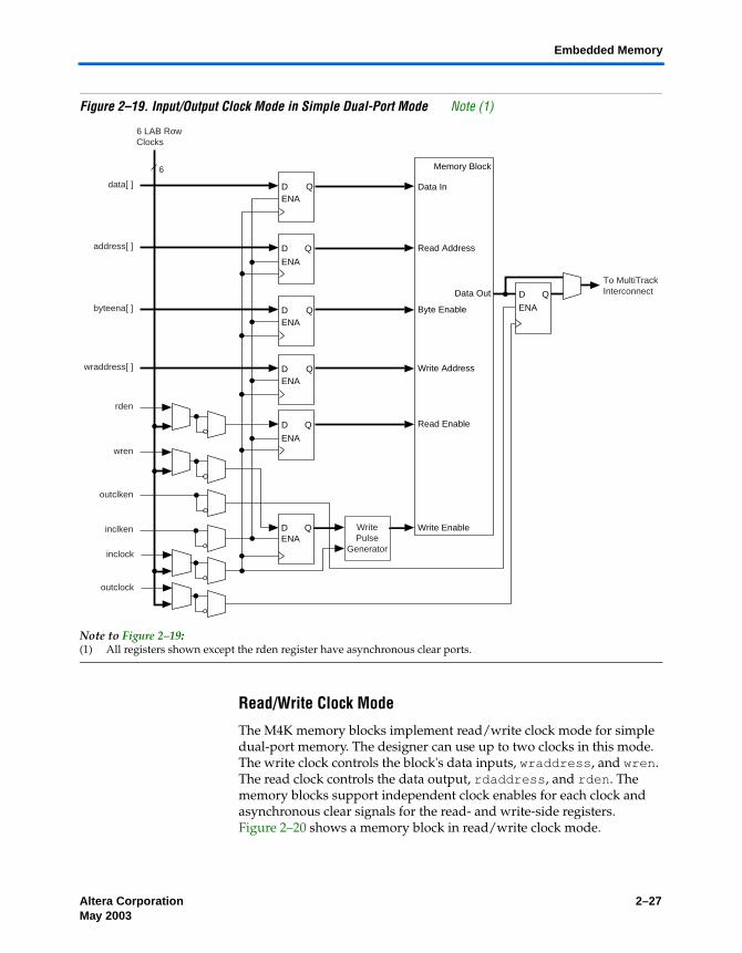
Altera Corporation 2–27May 2003 Preliminary
Embedded Memory
Figure 2–19. Input/Output Clock Mode in Simple Dual-Port Mode Note (1)
Note to Figure 2–19:(1) All registers shown except the rden register have asynchronous clear ports.
Read/Write Clock Mode
The M4K memory blocks implement read/write clock mode for simple dual-port memory. The designer can use up to two clocks in this mode. The write clock controls the block's data inputs, wraddress, and wren. The read clock controls the data output, rdaddress, and rden. The memory blocks support independent clock enables for each clock and asynchronous clear signals for the read- and write-side registers. Figure 2–20 shows a memory block in read/write clock mode.
6
DENA
Q
D
ENA
Q
D
ENA
Q
D
ENA
Q
DENA
Q
data[ ]
DENA
Qwraddress[ ]
address[ ]
Memory Block256 ´ 16512 ´ 8
1,024 ´ 42,048 ´ 24,096 ´ 1
Data In
Read Address
Write Address
Write Enable
Read Enable
Data Out
outclken
inclken
inclock
outclock
wren
rden
6 LAB Row Clocks
To MultiTrackInterconnect
DENA
Qbyteena[ ] Byte Enable
WritePulse
Generator

2–28 Altera CorporationPreliminary May 2003
Cyclone Device Handbook, Volume 1
Figure 2–20. Read/Write Clock Mode in Simple Dual-Port Mode Note (1)
Note to Figure 2–20:(1) All registers shown except the rden register have asynchronous clear ports.
Single-Port Mode
The M4K memory blocks also support single-port mode, used when simultaneous reads and writes are not required. See Figure 2–21. A single M4K memory block can support up to two single-port mode RAM blocks if each RAM block is less than or equal to 2K bits in size.
6
DENA
Q
D
ENA
Q
D
ENA
Q
D
ENA
Q
DENA
Q
data[ ]
DENA
Qwraddress[ ]
address[ ]
Memory Block256 × 16512 × 8
1,024 × 42,048 × 24,096 × 1
Data In
Read Address
Write Address
Write Enable
Read Enable
Data Out
rdclken
wrclken
wrclock
rdclock
wren
rden
6 LAB RowClocks
To MultiTrackInterconnect
DENA
Qbyteena[ ] Byte Enable
WritePulse
Generator

Altera Corporation 2–29May 2003 Preliminary
Global Clock Network & Phase-Locked Loops
Figure 2–21. Single-Port Mode
Global Clock Network & Phase-Locked Loops
Cyclone devices provide a global clock network and up to two PLLs for a complete clock management solution.
Global Clock Network
There are four dedicated clock pins (CLK[3..0], two pins on the left side and two pins on the right side) that drive the global clock network, as shown in Figure 2–22. PLL outputs, logic array, and dual-purpose clock (DPCLK[7..0]) pins can also drive the global clock network.
The eight global clock lines in the global clock network drive throughout the entire device. The global clock network can provide clocks for all resources within the device IOEs, LEs, and memory blocks. The global clock lines can also be used for control signals, such as clock enables and synchronous or asynchronous clears fed from the external pin, or DQS signals for DDR SDRAM or FCRAM interfaces. Internal logic can also drive the global clock network for internally generated global clocks and
6
DENA
Q
D
ENA
Q
D
ENA
Q
DENA
Q
data[ ]
address[ ]
RAM/ROM256 × 16512 × 8
1,024 × 42,048 × 24,096 × 1
Data In
Address
Write Enable
Data Out
outclken
inclken
inclock
outclock
WritePulse
Generator
wren
6 LAB RowClocks
To MultiTrackInterconnect

2–30 Altera CorporationPreliminary May 2003
Cyclone Device Handbook, Volume 1
asynchronous clears, clock enables, or other control signals with large fanout. Figure 2–22 shows the various sources that drive the global clock network.
Figure 2–22. Global Clock Generation Note (1)
Notes to Figure 2–22:(1) The EP1C3 device in the 100-pin TQFP package has five DPCLK pins (DPCLK2, DPCLK3, DPCLK4, DPCLK6, and
DPCLK7).(2) EP1C3 devices only contain one PLL (PLL 1).(3) The EP1C3 device in the 100-pin TQFP package does not have dedicated clock pins CLK1 and CLK3.
Dual-Purpose Clock Pins
Each Cyclone device except the EP1C3 device has eight dual-purpose clock pins, DPCLK[7..0] (two on each I/O bank). EP1C3 devices have five DPCLK pins in the 100-pin TQFP package. These dual-purpose pins
8
Global ClockNetwork
PLL1 PLL2(2)
CLK0
CLK1 (3)CLK2
CLK3 (3)
DPCLK1
DPCLK0
DPCLK4
DPCLK5
DPCLK2 DPCLK3
DPCLK7 DPCLK6
2 2
From logicarray
From logicarray
4
4 4
4
Cyclone Device
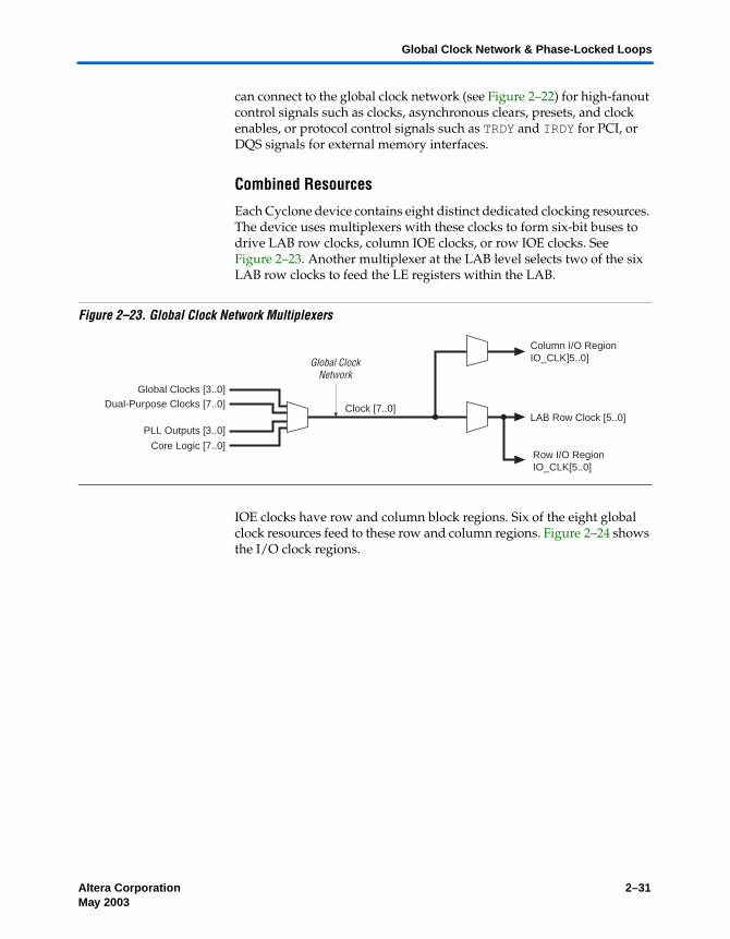
Altera Corporation 2–31May 2003 Preliminary
Global Clock Network & Phase-Locked Loops
can connect to the global clock network (see Figure 2–22) for high-fanout control signals such as clocks, asynchronous clears, presets, and clock enables, or protocol control signals such as TRDY and IRDY for PCI, or DQS signals for external memory interfaces.
Combined Resources
Each Cyclone device contains eight distinct dedicated clocking resources. The device uses multiplexers with these clocks to form six-bit buses to drive LAB row clocks, column IOE clocks, or row IOE clocks. See Figure 2–23. Another multiplexer at the LAB level selects two of the six LAB row clocks to feed the LE registers within the LAB.
Figure 2–23. Global Clock Network Multiplexers
IOE clocks have row and column block regions. Six of the eight global clock resources feed to these row and column regions. Figure 2–24 shows the I/O clock regions.
Clock [7..0]
Column I/O RegionIO_CLK]5..0]
LAB Row Clock [5..0]
Row I/O RegionIO_CLK[5..0]
Global Clocks [3..0]
PLL Outputs [3..0]
Dual-Purpose Clocks [7..0]
Global ClockNetwork
Core Logic [7..0]

2–32 Altera CorporationPreliminary May 2003
Cyclone Device Handbook, Volume 1
Figure 2–24. I/O Clock Regions
PLLs
Cyclone PLLs provide general-purpose clocking with clock multiplication and phase shifting as well as outputs for differential I/O support. Cyclone devices contain two PLLs, except for the EP1C3 device, which contains one PLL.
Column I/O Clock RegionIO_CLK[5..0]
Column I/O Clock RegionIO_CLK[5..0]
6
6
I/O Clock Regions
I/O Clock Regions
8
Global ClockNetwork
RowI/O Regions
Cyclone Logic Array
6
6
LAB Row Clockslabclk[5..0]
LAB Row Clockslabclk[5..0]
LAB Row Clockslabclk[5..0]
LAB Row Clockslabclk[5..0]
LAB Row Clockslabclk[5..0]
LAB Row Clockslabclk[5..0]
6
6
6
6

Altera Corporation 2–33May 2003 Preliminary
Global Clock Network & Phase-Locked Loops
Table 2–6 shows the PLL features in Cyclone devices. Figure 2–25 shows a Cyclone PLL.
Figure 2–25. Cyclone PLL Note (1)
Notes to Figure 2–25:(1) The EP1C3 device in the 100-pin TQFP package does not support external outputs or LVDS inputs. The EP1C6
device in the 144-pin TQFP package does not support external output from PLL2.(2) LVDS input is supported via the secondary function of the dedicated clock pins. For PLL 1, the CLK0 pin’s
secondary function is LVDSCLK1p and the CLK1 pin’s secondary function is LVDSCLK1n. For PLL 2, the CLK2 pin’s secondary function is LVDSCLK2p and the CLK3 pin’s secondary function is LVDSCLK2n.
(3) PFD: phase frequency detector.
Table 2–6. Cyclone PLL Features
Feature PLL Support
Clock multiplication and division m/(n × post-scale counter) (1)
Phase shift Down to 156-ps increments (2), (3)
Programmable duty cycle Yes
Number of internal clock outputs 2
Number of external clock outputs One differential or one single-ended (4)
Notes to Table 2–6:(1) The m counter ranges from 2 to 32. The n counter and the post-scale counters
range from 1 to 32.(2) The smallest phase shift is determined by the voltage-controlled oscillator (VCO)
period divided by 8.(3) For degree increments, Cyclone devices can shift all output frequencies in
increments of 45°. Smaller degree increments are possible depending on the frequency and divide parameters.
(4) The EP1C3 device in the 100-pin TQFP package does not support external clock output. The EP1C6 device in the 144-pin TQFP package does not support external clock output from PLL2.
ChargePump
VCOPFD (3) LoopFilter
CLK0 orLVDSCLK1p (2)
CLK1 orLVDSCLK1n (2)
÷n
÷m
∆t
∆t
Global clock
Global clock
I/O buffer
÷g0
÷g1
÷e
VCO Phase SelectionSelectable at Each PLL
Output Port
Post-ScaleCounters

2–34 Altera CorporationPreliminary May 2003
Cyclone Device Handbook, Volume 1
Figure 2–26 shows the PLL global clock connections.
Figure 2–26. Cyclone PLL Global Clock Connections
Notes to Figure 2–26:(1) PLL 1 supports one single-ended or LVDS input via pins CLK0 and CLK1.(2) PLL2 supports one single-ended or LVDS input via pins CLK2 and CLK3.(3) PLL1_OUT and PLL2_OUT support single-ended or LVDS output. If external output is not required, these pins are
available as regular user I/O pins.(4) The EP1C3 device in the 100-pin TQFP package does not support external clock output. The EP1C6 device in the
144-pin TQFP package does not support external clock output from PLL2.
Table 2–7 shows the global clock network sources available in Cyclone devices.
CLK0
CLK1 (1)PLL1 PLL2
g0
g1
e
g0
g1
e
PLL1_OUT (3), (4)
CLK2
CLK3 (2)
PLL2_OUT (3), (4)
G0 G2
G1 G3
G4 G6
G5 G7
Table 2–7. Global Clock Network Sources (Part 1 of 2)
Source GCLK0 GCLK1 GCLK2 GCLK3 GCLK4 GCLK5 GCLK6 GCLK7
PLL Counter Output
PLL1 G0 v v
PLL1 G1 v v
PLL2 G0 (1) v v
PLL2 G1 (1) v v
Dedicated Clock Input Pins
CLK0 v v
CLK1 (2) v v
CLK2 v v
CLK3 (2) v v

Altera Corporation 2–35May 2003 Preliminary
Global Clock Network & Phase-Locked Loops
Clock Multiplication & Division
Cyclone PLLs provide clock synthesis for PLL output ports using m/(n × post scale counter) scaling factors. The input clock is divided by a pre-scale divider, n, and is then multiplied by the m feedback factor. The control loop drives the VCO to match fIN × (m/n). Each output port has a unique post-scale counter to divide down the high-frequency VCO. For multiple PLL outputs with different frequencies, the VCO is set to the least-common multiple of the output frequencies that meets its frequency specifications. Then, the post-scale dividers scale down the output frequency for each output port. For example, if the output frequencies required from one PLL are 33 and 66 MHz, the VCO is set to 330 MHz (the least-common multiple in the VCO's range).
Each PLL has one pre-scale divider, n, that can range in value from 1 to 32. Each PLL also has one multiply divider, m, that can range in value from 2 to 32. Global clock outputs have two post scale G dividers for global clock outputs, and external clock outputs have an E divider for external clock output, both ranging from 1 to 32. The Quartus II® software automatically chooses the appropriate scaling factors according to the input frequency, multiplication, and division values entered.
Dual-Purpose Clock Pins
DPCLK0 (3) v
DPCLK1 (3) v
DPCLK2 v
DPCLK3 v
DPCLK4 v
DPCLK5 (3) v
DPCLK6 v
DPCLK7 v
Notes to Table 2–7:(1) EP1C3 devices only have one PLL (PLL 1).(2) EP1C3 devices in the 100-pin TQFP package do not have dedicated clock pins CLK1 and CLK3.(3) EP1C3 devices in the 100-pin TQFP package do not have the DPCLK0, DPCLK1, or DPCLK5 pins.
Table 2–7. Global Clock Network Sources (Part 2 of 2)
Source GCLK0 GCLK1 GCLK2 GCLK3 GCLK4 GCLK5 GCLK6 GCLK7

2–36 Altera CorporationPreliminary May 2003
Cyclone Device Handbook, Volume 1
External Clock Inputs
Each PLL supports single-ended or differential inputs for source-synchronous receivers or for general-purpose use. The dedicated clock pins (CLK[3..0]) feed the PLL inputs. These dual-purpose pins can also act as LVDS input pins. See Figure 2–25.
Table 2–8 shows the I/O standards supported by PLL input and output pins.
For more information on LVDS I/O support, see “LVDS I/O Pins” on page 2–54.
External Clock Outputs
Each PLL supports one differential or one single-ended output for source-synchronous transmitters or for general-purpose external clocks. If the PLL does not use these PLL_OUT pins, the pins are available for use as general-purpose I/O pins. The PLL_OUT pins support all I/O standards shown in Table 2–8.
The external clock outputs do not have their own VCC and ground voltage supplies. Therefore, to minimize jitter, do not place switching I/O pins next to these output pins. The EP1C3 device in the 100-pin TQFP package
Table 2–8. PLL I/O Standards
I/O Standard CLK Input EXTCLK Output
3.3-V LVTTL/LVCMOS v v
2.5-V LVTTL/LVCMOS v v
1.8-V LVTTL/LVCMOS v v
1.5-V LVCMOS v v
3.3-V PCI v v
LVDS v v
SSTL-2 class I v v
SSTL-2 class II v v
SSTL-3 class I v v
SSTL-3 class II v v
Differential SSTL-2 v

Altera Corporation 2–37May 2003 Preliminary
Global Clock Network & Phase-Locked Loops
does not have dedicated clock output pins. The EP1C6 device in the 144-pin TQFP package only supports dedicated clock outputs from PLL 1.
Clock Feedback
Cyclone PLLs have three modes for multiplication and/or phase shifting:
Zero delay buffer modeThe external clock output pin is phase-aligned with the clock input pin for zero delay.
Normal modeIf the design uses an internal PLL clock output, the normal mode compensates for the internal clock delay from the input clock pin to the IOE registers. The external clock output pin is phase shifted with respect to the clock input pin if connected in this mode. The designer defines which internal clock output from the PLL should be phase-aligned to compensate for internal clock delay.
No compensation modeIn this mode, the PLL will not compensate for any clock networks.
Phase Shifting
Cyclone PLLs have an advanced clock shift capability that enables programmable phase shifts. Designers can enter a phase shift (in degrees or time units) for each PLL clock output port or for all outputs together in one shift. Designers can perform phase shifting in time units with a resolution range of 156 to 417 ps. The finest resolution equals one eighth of the VCO period. The VCO period is a function of the frequency input and the multiplication and division factors. Each clock output counter can choose a different phase of the VCO period from up to eight taps. Designers can use this clock output counter along with an initial setting on the post-scale counter to achieve a phase-shift range for the entire period of the output clock. The phase tap feedback to the m counter can shift all outputs to a single phase. The Quartus II® software automatically sets the phase taps and counter settings according to the phase shift entered.
Lock Detect Signal
The lock output indicates that there is a stable clock output signal in phase with the reference clock. Without any additional circuitry, the lock signal may toggle as the PLL begins tracking the reference clock. Therefore, the designer may need to gate the lock signal for use as a system-control signal.

2–38 Altera CorporationPreliminary May 2003
Cyclone Device Handbook, Volume 1
Programmable Duty Cycle
The programmable duty cycle allows PLLs to generate clock outputs with a variable duty cycle. This feature is supported on each PLL post-scale counter (g0, g1, e). The duty cycle setting is achieved by a low- and high-time count setting for the post-scale dividers. The Quartus II® software uses the frequency input and the required multiply or divide rate to determine the duty cycle choices.
Control Signals
There are three control signals for clearing and enabling PLLs and their outputs. The designer can use these signals to control PLL resynchronization and the ability to gate PLL output clocks for low-power applications.
The pllenable signal enables and disables PLLs. When the pllenable signal is low, the clock output ports are driven by ground and all the PLLs go out of lock. When the pllenable signal goes high again, the PLLs relock and resynchronize to the input clocks. An input pin or LE output can drive the pllenable signal.
The areset signals are reset/resynchronization inputs for each PLL. Cyclone devices can drive these input signals from input pins or from LEs. When areset is driven high, the PLL counters will reset, clearing the PLL output and placing the PLL out of lock. When driven low again, the PLL will resynchronize to its input as it relocks.
The pfdena signals control the phase frequency detector (PFD) output with a programmable gate. If you disable the PFD, the VCO will operate at its last set value of control voltage and frequency with some drift, and the system will continue running when the PLL goes out of lock or the input clock disables. By maintaining the last locked frequency, the system has time to store its current settings before shutting down. The designer can either use their own control signal or gated locked status signals to trigger the pfdena signal.
f For more information on Cyclone PLLs, see Chapter 6, Using PLLs in Cyclone Devices.

Altera Corporation 2–39May 2003 Preliminary
I/O Structure
I/O Structure IOEs support many features, including:
Differential and single-ended I/O standards 3.3-V, 32-bit, 66-MHz PCI compliance Joint Test Action Group (JTAG) boundary-scan test (BST) support Output drive strength control Weak pull-up resistors during configuration Slew-rate control Tri-state buffers Bus-hold circuitry Programmable pull-up resistors in user mode Programmable input and output delays Open-drain outputs DQ and DQS I/O pins
Cyclone device IOEs contain a bidirectional I/O buffer and three registers for complete embedded bidirectional single data rate transfer. Figure 2–27 shows the Cyclone IOE structure. The IOE contains one input register, one output register, and one output enable register. The designer can use the input registers for fast setup times and output registers for fast clock-to-output times. Additionally, the designer can use the output enable (OE) register for fast clock-to-output enable timing. The Quartus®II software automatically duplicates a single OE register that controls multiple output or bidirectional pins. IOEs can be used as input, output, or bidirectional pins.

2–40 Altera CorporationPreliminary May 2003
Cyclone Device Handbook, Volume 1
Figure 2–27. Cyclone IOE Structure
Note to Figure 2–27:(1) There are two paths available for combinatorial inputs to the logic array. Each path
contains a unique programmable delay chain.
The IOEs are located in I/O blocks around the periphery of the Cyclone device. There are up to three IOEs per row I/O block and up to three IOEs per column I/O block (column I/O blocks span two columns). The row I/O blocks drive row, column, or direct link interconnects. The column I/O blocks drive column interconnects. Figure 2–28 shows how a row I/O block connects to the logic array. Figure 2–29 shows how a column I/O block connects to the logic array.
Output Register
Output
Combinatorialinput (1)
Input
OE Register
OE
Input Register
Logic Array
D Q
D Q
D Q

Altera Corporation 2–41May 2003 Preliminary
I/O Structure
Figure 2–28. Row I/O Block Connection to the Interconnect
Notes to Figure 2–28:(1) The 21 data and control signals consist of three data out lines, io_dataout[2..0], three output enables,
io_coe[2..0], three input clock enables, io_cce_in[2..0], three output clock enables, io_cce_out[2..0], three clocks, io_cclk[2..0], three asynchronous clear signals, io_caclr[2..0], and three synchronous clear signals, io_csclr[2..0].
(2) Each of the three IOEs in the row I/O block can have one io_datain input (combinatorial or registered) and one comb_io_datain (combinatorial) input.
21
R4 Interconnects C4 Interconnects
I/O Block Local Interconnect
21 Data andControl Signalsfrom Logic Array (1)
io_datain[2..0] andcomb_io_datain[2..0] (2)
io_clk[5:0]
Row I/O BlockContains up to
Three IOEs
Direct LinkInterconnect
to Adjacent LAB
Direct LinkInterconnect
from Adjacent LAB
LAB LocalInterconnect
LAB RowI/O Block

2–42 Altera CorporationPreliminary May 2003
Cyclone Device Handbook, Volume 1
Figure 2–29. Column I/O Block Connection to the Interconnect
Notes to Figure 2–29:(1) The 21 data and control signals consist of three data out lines, io_dataout[2..0], three output enables,
io_coe[2..0], three input clock enables, io_cce_in[2..0], three output clock enables, io_cce_out[2..0], three clocks, io_cclk[2..0], three asynchronous clear signals, io_caclr[2..0], and three synchronous clear signals, io_csclr[2..0].
(2) Each of the three IOEs in the column I/O block can have one io_datain input (combinatorial or registered) and one comb_io_datain (combinatorial) input.
21 Data &Control Signals
from Logic Array (1)
Column I/O Block Containsup to Three IOEs
I/O BlockLocal Interconnect
IO_datain[2:0] &comb_io_datain[2..0]
(2)
R4 Interconnects
LAB LocalInterconnect
C4 Interconnects
21
LAB LAB LAB
io_clk[5..0]
Column I/O Block

Altera Corporation 2–43May 2003 Preliminary
I/O Structure
The pin's datain signals can drive the logic array. The logic array drives the control and data signals, providing a flexible routing resource. The row or column IOE clocks, io_clk[5..0], provide a dedicated routing resource for low-skew, high-speed clocks. The global clock network generates the IOE clocks that feed the row or column I/O regions (see “Global Clock Network & Phase-Locked Loops” on page 2–29). Figure 2–30 illustrates the signal paths through the I/O block.
Figure 2–30. Signal Path through the I/O Block
Each IOE contains its own control signal selection for the following control signals: oe, ce_in, ce_out, aclr/preset, sclr/preset, clk_in, and clk_out. Figure 2–31 illustrates the control signal selection.
Row or Columnio_clk[5..0]
io_datain
comb_io_datain
io_dataout
io_coe
oe
ce_in
ce_out
io_cce_inaclr/preset
io_cce_outsclr
io_caclrclk_in
io_cclkclk_out
dataout
Data andControlSignal
Selection
IOE
To LogicArray
From LogicArray
To OtherIOEs
io_csclr

2–44 Altera CorporationPreliminary May 2003
Cyclone Device Handbook, Volume 1
Figure 2–31. Control Signal Selection per IOE
In normal bidirectional operation, the designer can use the input register for input data requiring fast setup times. The input register can have its own clock input and clock enable separate from the OE and output registers. The output register can be used for data requiring fast clock-to-output performance. The OE register is available for fast clock-to-output enable timing. The OE and output register share the same clock source and the same clock enable source from the local interconnect in the associated LAB, dedicated I/O clocks, or the column and row interconnects. Figure 2–32 shows the IOE in bidirectional configuration.
clk_out
ce_inclk_in
ce_out
aclr/preset
sclr/preset
Dedicated I/OClock [5..0]
LocalInterconnect
LocalInterconnect
LocalInterconnect
LocalInterconnect
LocalInterconnect
oe
io_coe
io_caclr
LocalInterconnect
io_csclr
io_cce_out
io_cce_in
io_cclk

Altera Corporation 2–45May 2003 Preliminary
I/O Structure
Figure 2–32. Cyclone IOE in Bidirectional I/O Configuration
The Cyclone device IOE includes programmable delays to ensure zero hold times, minimize setup times, or increase clock to output times.
A path in which a pin directly drives a register may require a programmable delay to ensure zero hold time, whereas a path in which a pin drives a register through combinatorial logic may not require the delay. Programmable delays decrease input-pin-to-logic-array and IOE input register delays. The Quartus II® Compiler can program these delays to automatically minimize setup time while providing a zero hold
Chip-Wide Reset
OE Register
VCCIO
OptionalPCI Clamp
Column or RowInterconect
ioe_clk[5..0]
Input RegisterInput Pin to
Input Register Delayor Input Pin to
Logic Array Delay
Input Pin toLogic Array Delay
Drive Strength Control
Open-Drain Output
Slew Controlsclr/preset
OE
clkout
ce_out
aclr/prn
clkin
ce_in
OutputPin Delay
ProgrammablePull-UpResistor
Bus Hold
PRN
CLRN
D Q
Output Register
PRN
CLRN
D Q
PRN
CLRN
D Q
VCCIO
comb_datain
data_in
ENA
ENA
ENA

2–46 Altera CorporationPreliminary May 2003
Cyclone Device Handbook, Volume 1
time. Programmable delays can increase the register-to-pin delays for output registers. Table 2–9 shows the programmable delays for Cyclone devices.
There are two paths in the IOE for a combinatorial input to reach the logic array. Each of the two paths can have a different delay. This allows the designer to adjust delays from the pin to internal LE registers that reside in two different areas of the device. The designer sets the two combinatorial input delays by selecting different delays for two different paths under the Decrease input delay to internal cells logic option in the Quartus II® software. When the input signal requires two different delays for the combinatorial input, the input register in the IOE is no longer available.
The IOE registers in Cyclone devices share the same source for clear or preset. The designer can program preset or clear for each individual IOE. The designer can also program the registers to power up high or low after configuration is complete. If programmed to power up low, an asynchronous clear can control the registers. If programmed to power up high, an asynchronous preset can control the registers. This feature prevents the inadvertent activation of another device's active-low input upon power up. If one register in an IOE uses a preset or clear signal then all registers in the IOE must use that same signal if they require preset or clear. Additionally a synchronous reset signal is available to the designer for the IOE registers.
External RAM Interfacing
Cyclone devices support DDR SDRAM and FCRAM interfaces at up to 133 MHz through dedicated circuitry.
DDR SDRAM & FCRAM
Cyclone devices have dedicated circuitry for interfacing with DDR SDRAM. All I/O banks support DDR SDRAM and FCRAM I/O pins. However, the configuration input pins in bank 1 must operate at 2.5 V because the SSTL-2 VCCIO level is 2.5 V. Additionally, the configuration
Table 2–9. Cyclone Programmable Delay Chain
Programmable Delays Quartus II® Logic Option
Input pin to logic array delay Decrease input delay to internal cells
Input pin to input register delay Decrease input delay to input registers
Output pin delay Increase delay to output pin

Altera Corporation 2–47May 2003 Preliminary
I/O Structure
output pins (nSTATUS and CONF_DONE) and all the JTAG pins in I/O bank 3 must operate at 2.5 V because the VCCIO level of SSTL-2 is 2.5 V. I/O banks 1, 2, 3, and 4 support DQS signals with DQ bus modes of × 8.
For × 8 mode, there are up to eight groups of programmable DQS and DQ pins, I/O banks 1, 2, 3, and 4 each have two groups in the 324-pin and 400-pin FineLine BGA packages. Each group consists of one DQS pin, a set of eight DQ pins, and one DM pin (see Figure 2–33). Each DQS pin drives the set of eight DQ pins within that group.
Figure 2–33. Cyclone Device DQ & DQS Groups in × 8 Mode Note (1)
Note to Figure 2–33:(1) Each DQ group consists of one DQS pin, eight DQ pins, and one DM pin.
Table 2–10 shows the number of DQ pin groups per device.
DQ Pins DQS Pin DM Pin
Top, Bottom, Left, or Right I/O Bank
Table 2–10. DQ Pin Groups (Part 1 of 2)
Device Package Number of × 8 DQ Pin Groups
Total DQ Pin Count
EP1C3 100-pin TQFP (1) 3 24
144-pin TQFP 4 32
EP1C4 324-pin FineLine BGA 8 64
400-pin FineLine BGA 8 64

2–48 Altera CorporationPreliminary May 2003
Cyclone Device Handbook, Volume 1
A programmable delay chain on each DQS pin allows for either a 90° phase shift (for DDR SDRAM), or a 72° phase shift (for FCRAM) which automatically center-aligns input DQS synchronization signals within the data window of their corresponding DQ data signals. The phase-shifted DQS signals drive the global clock network. This global DQS signal clocks DQ signals on internal LE registers.
These DQS delay elements combine with the PLL’s clocking and phase shift ability to provide a complete hardware solution for interfacing to high-speed memory.
The clock phase shift allows the PLL to clock the DQ output enable and output paths. The designer should use the following guidelines to meet 133 MHz performance for DDR SDRAM and FCRAM interfaces:
The DQS signal must be in the middle of the DQ group it clocks Resynchronize the incoming data to the logic array clock using
successive LE registers or FIFO buffers LE registers must be placed in the LAB adjacent to the DQ I/O pin
column it is fed by
Figure 2–34 illustrates DDR SDRAM and FCRAM interfacing from the I/O through the dedicated circuitry to the logic array.
EP1C6 144-pin TQFP 4 32
240-pin PQFP 4 32
256-pin FineLine BGA 4 32
EP1C12 240-pin PQFP 4 32
256-pin FineLine BGA 4 32
324-pin FineLine BGA 8 64
EP1C20 324-pin FineLine BGA 8 64
400-pin FineLine BGA 8 64
Note to Table 2–10:(1) EP1C3 devices in the 100-pin TQFP package do not have any DQ pin groups in
I/O bank 1.
Table 2–10. DQ Pin Groups (Part 2 of 2)
Device Package Number of × 8 DQ Pin Groups
Total DQ Pin Count

Altera Corporation 2–49May 2003 Preliminary
I/O Structure
Figure 2–34. DDR SDRAM & FCRAM Interfacing
Programmable Drive Strength
The output buffer for each Cyclone device I/O pin has a programmable drive strength control for certain I/O standards. The LVTTL and LVCMOS standards have several levels of drive strength that the designer can control. SSTL-3 class I and II, and SSTL-2 class I and II support a minimum setting, the lowest drive strength that guarantees the IOH/IOL of the standard. Using minimum settings provides signal slew
VCC
GND
PLL
Phase Shifted -90˚
DQS
Adjacent LAB LEs
Global Clock
ResynchronizingGlobal Clock
ProgrammableDelay Chain
Output LERegister
Output LERegisters
DQ
Input LERegisters
Input LERegisters
LERegister
LERegister
∆ t
AdjacentLAB LEs
OE OE LERegister
OE LERegister
OE OE LERegister
OE LERegister
Output LERegisters
Output LERegister
DataA
DataB
clk
-90˚ clk
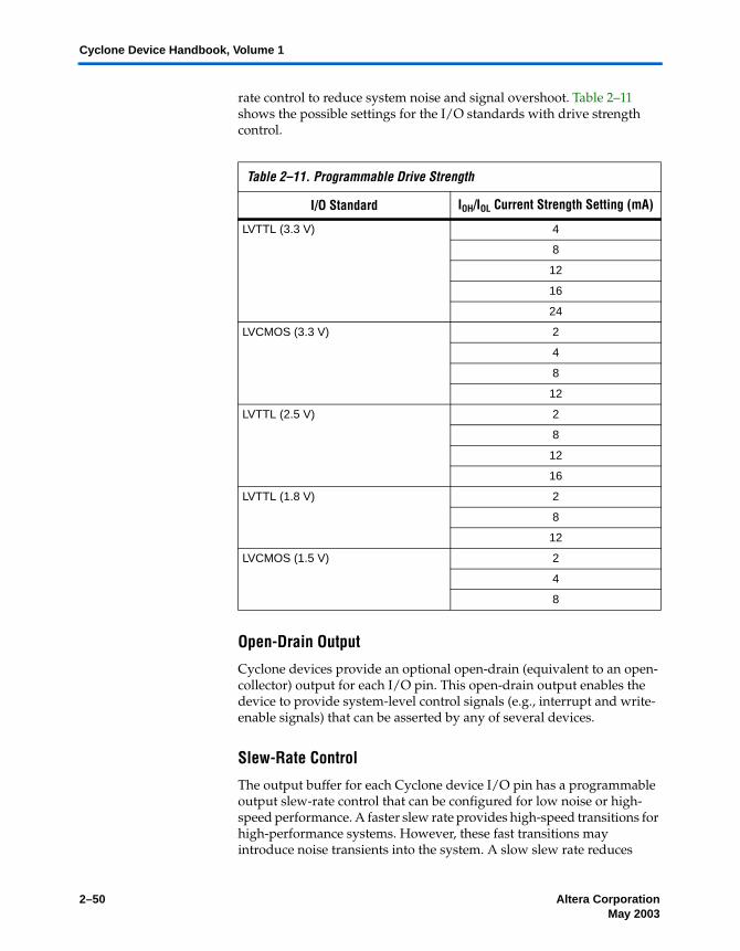
2–50 Altera CorporationPreliminary May 2003
Cyclone Device Handbook, Volume 1
rate control to reduce system noise and signal overshoot. Table 2–11 shows the possible settings for the I/O standards with drive strength control.
Open-Drain Output
Cyclone devices provide an optional open-drain (equivalent to an open-collector) output for each I/O pin. This open-drain output enables the device to provide system-level control signals (e.g., interrupt and write-enable signals) that can be asserted by any of several devices.
Slew-Rate Control
The output buffer for each Cyclone device I/O pin has a programmable output slew-rate control that can be configured for low noise or high-speed performance. A faster slew rate provides high-speed transitions for high-performance systems. However, these fast transitions may introduce noise transients into the system. A slow slew rate reduces
Table 2–11. Programmable Drive Strength
I/O Standard IOH/IOL Current Strength Setting (mA)
LVTTL (3.3 V) 4
8
12
16
24
LVCMOS (3.3 V) 2
4
8
12
LVTTL (2.5 V) 2
8
12
16
LVTTL (1.8 V) 2
8
12
LVCMOS (1.5 V) 2
4
8

Altera Corporation 2–51May 2003 Preliminary
I/O Structure
system noise, but adds a nominal delay to rising and falling edges. Each I/O pin has an individual slew-rate control, allowing the designer to specify the slew rate on a pin-by-pin basis. The slew-rate control affects both the rising and falling edges.
Bus Hold
Each Cyclone device I/O pin provides an optional bus-hold feature. The bus-hold circuitry can hold the signal on an I/O pin at its last-driven state. Since the bus-hold feature holds the last-driven state of the pin until the next input signal is present, an external pull-up or pull-down resistor is not necessary to hold a signal level when the bus is tri-stated.
The bus-hold circuitry also pulls undriven pins away from the input threshold voltage where noise can cause unintended high-frequency switching. The designer can select this feature individually for each I/O pin. The bus-hold output will drive no higher than VCCIO to prevent overdriving signals. If the bus-hold feature is enabled, the device cannot use the programmable pull-up option. Disable the bus-hold feature when the I/O pin is configured for differential signals.
The bus-hold circuitry uses a resistor with a nominal resistance (RBH) of approximately 7 kΩ to pull the signal level to the last-driven state. Table 4–15 on page 4–6 gives the specific sustaining current for each VCCIO voltage level driven through this resistor and overdrive current used to identify the next-driven input level.
The bus-hold circuitry is only active after configuration. When going into user mode, the bus-hold circuit captures the value on the pin present at the end of configuration.
Programmable Pull-Up Resistor
Each Cyclone device I/O pin provides an optional programmable pull-up resistor during user mode. If the designer enables this feature for an I/O pin, the pull-up resistor (typically 25 kΩ) holds the output to the VCCIO level of the output pin's bank.

2–52 Altera CorporationPreliminary May 2003
Cyclone Device Handbook, Volume 1
Advanced I/O Standard Support
Cyclone device IOEs support the following I/O standards:
3.3-V LVTTL/LVCMOS 2.5-V LVTTL/LVCMOS 1.8-V LVTTL/LVCMOS 1.5-V LVCMOS 3.3-V PCI LVDS SSTL-2 class I and II SSTL-3 class I and II Differential SSTL-2 class II (on output clocks only)
Table 2–12 describes the I/O standards supported by Cyclone devices.
Cyclone devices contain four I/O banks, as shown in Figure 2–35. I/O banks 1 and 3 support all the I/O standards listed in Table 2–12. I/O banks 2 and 4 support all the I/O standards listed in Table 2–12 except the 3.3-V PCI standard. I/O banks 2 and 4 contain dual-purpose DQS, DQ, and DM pins to support a DDR SDRAM or FCRAM interface. I/O bank 1 can also support a DDR SDRAM or FCRAM interface, however, the configuration input pins in I/O bank 1 must operate at 2.5 V. I/O bank 3 can also support a DDR SDRAM or FCRAM interface, however, all the JTAG pins in I/O bank 3 must operate at 2.5 V.
Table 2–12. Cyclone I/O Standards
I/O Standard TypeInput Reference
Voltage (VREF) (V)Output Supply
Voltage (VCCIO) (V)
Board Termination
Voltage (VTT) (V)
3.3-V LVTTL/LVCMOS Single-ended N/A 3.3 N/A
2.5-V LVTTL/LVCMOS Single-ended N/A 2.5 N/A
1.8-V LVTTL/LVCMOS Single-ended N/A 1.8 N/A
1.5-V LVCMOS Single-ended N/A 1.5 N/A
3.3-V PCI (1) Single-ended N/A 3.3 N/A
LVDS (2) Differential N/A 2.5 N/A
SSTL-2 class I and II Voltage-referenced 1.25 2.5 1.25
SSTL-3 class I and II Voltage-referenced 1.5 3.3 1.5
Differential SSTL-2 (3) Differential 1.25 2.5 1.25
Notes to Table 2–12:(1) EP1C3 devices do not support PCI.(2) EP1C3 devices in the 100-pin TQFP package do not support the LVDS I/O standard.(3) This I/O standard is only available on output clock pins (PLL_OUT pins).

Altera Corporation 2–53May 2003 Preliminary
I/O Structure
Figure 2–35. Cyclone I/O Banks Notes (1), (2)
Notes to Figure 2–35:(1) Figure 2–35 is a top view of the silicon die.(2) Figure 2–35 is a graphic representation only. Refer to the pin list and the Quartus II® software for exact pin locations.
Each I/O bank has its own VCCIO pins. A single device can support 1.5-V, 1.8-V, 2.5-V, and 3.3-V interfaces; each individual bank can support a different standard with different I/O voltages. Each bank also has dual-purpose VREF pins to support any one of the voltage-referenced standards (e.g., SSTL-3) independently. If an I/O bank does not use voltage-referenced standards, the VREF pins are available as user I/O pins.
Each I/O bank can support multiple standards with the same VCCIO for input and output pins. For example, when VCCIO is 3.3-V, a bank can support LVTTL, LVCMOS, 3.3-V PCI, and SSTL-3 for inputs and outputs.
I/O Bank 2
I/O Bank 3
I/O Bank 4
I/O Bank 1
All I/O Banks Support 3.3-V LVTTL/LVCMOS 2.5-V LVTTL/LVCMOS 1.8-V LVTTL/LVCMOS 1.5-V LVCMOS LVDS SSTL-2 Class I and II SSTL-3 Class I and II
I/O Bank 3Also Supportsthe 3.3-V PCII/O Standard
I/O Bank 1Also Supportsthe 3.3-V PCII/O Standard
IndividualPower Bus
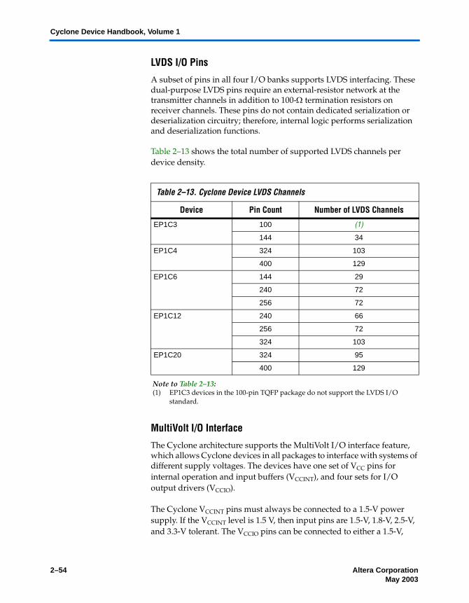
2–54 Altera CorporationPreliminary May 2003
Cyclone Device Handbook, Volume 1
LVDS I/O Pins
A subset of pins in all four I/O banks supports LVDS interfacing. These dual-purpose LVDS pins require an external-resistor network at the transmitter channels in addition to 100-Ω termination resistors on receiver channels. These pins do not contain dedicated serialization or deserialization circuitry; therefore, internal logic performs serialization and deserialization functions.
Table 2–13 shows the total number of supported LVDS channels per device density.
MultiVolt I/O Interface
The Cyclone architecture supports the MultiVolt I/O interface feature, which allows Cyclone devices in all packages to interface with systems of different supply voltages. The devices have one set of VCC pins for internal operation and input buffers (VCCINT), and four sets for I/O output drivers (VCCIO).
The Cyclone VCCINT pins must always be connected to a 1.5-V power supply. If the VCCINT level is 1.5 V, then input pins are 1.5-V, 1.8-V, 2.5-V, and 3.3-V tolerant. The VCCIO pins can be connected to either a 1.5-V,
Table 2–13. Cyclone Device LVDS Channels
Device Pin Count Number of LVDS Channels
EP1C3 100 (1)
144 34
EP1C4 324 103
400 129
EP1C6 144 29
240 72
256 72
EP1C12 240 66
256 72
324 103
EP1C20 324 95
400 129
Note to Table 2–13:(1) EP1C3 devices in the 100-pin TQFP package do not support the LVDS I/O
standard.

Altera Corporation 2–55May 2003 Preliminary
Power Sequencing & Hot Socketing
1.8-V, 2.5-V, or 3.3-V power supply, depending on the output requirements. The output levels are compatible with systems of the same voltage as the power supply (i.e., when VCCIO pins are connected to a 1.5-V power supply, the output levels are compatible with 1.5-V systems). When VCCIO pins are connected to a 3.3-V power supply, the output high is 3.3-V and is compatible with 3.3-V or 5.0-V systems. Table 2–14 summarizes Cyclone MultiVolt I/O support.
Power Sequencing & Hot Socketing
Because Cyclone devices can be used in a mixed-voltage environment, they have been designed specifically to tolerate any possible power-up sequence. Therefore, the VCCIO and VCCINT power supplies may be powered in any order.
Signals can be driven into Cyclone devices before and during power up without damaging the device. In addition, Cyclone devices do not drive out during power up. Once operating conditions are reached and the device is configured, Cyclone devices operate as specified by the user.
Table 2–14. Cyclone MultiVolt I/O Support Note (1)
VCCIO (V)Input Signal Output Signal
1.5 V 1.8 V 2.5 V 3.3 V 5.0 V 1.5 V 1.8 V 2.5 V 3.3 V 5.0 V
1.5 v v v (2) v (2) v
1.8 v v v v (3) v
2.5 v v v (5) v (5) v
3.3 v (4) v v (6) v (7) v (7) v (7) v v (8)
Notes to Table 2–14:(1) The PCI clamping diode must be disabled to drive an input with voltages higher than VCCIO.(2) When VCCIO = 1.5-V and a 2.5-V or 3.3-V input signal feeds an input pin, higher pin leakage current is expected.(3) When VCCIO = 1.8-V, a Cyclone device can drive a 1.5-V device with 1.8-V tolerant inputs.(4) When VCCIO = 3.3-V and a 2.5-V input signal feeds an input pin, the VCCIO supply current will be slightly larger
than expected.(5) When VCCIO = 2.5-V, a Cyclone device can drive a 1.5-V or 1.8-V device with 2.5-V tolerant inputs.(6) Cyclone devices can be 5.0-V tolerant with the use of an external resistor and the internal PCI clamp diode.(7) When VCCIO = 3.3-V, a Cyclone device can drive a 1.5-V, 1.8-V, or 2.5-V device with 3.3-V tolerant inputs.(8) When VCCIO = 3.3-V, a Cyclone device can drive a device with 5.0-V LVTTL inputs but not 5.0-V LVCMOS inputs.

2–56 Altera CorporationPreliminary May 2003
Cyclone Device Handbook, Volume 1

Altera Corporation 3–1May 2003 Preliminary
3. Configuration & Testing
IEEE Std. 1149.1 (JTAG) Boundary Scan Support
All Cyclone devices provide JTAG BST circuitry that complies with the IEEE Std. 1149.1a-1990 specification. JTAG boundary-scan testing can be performed either before or after, but not during configuration. Cyclone devices can also use the JTAG port for configuration together with either the Quartus II® software or hardware using either Jam Files (.jam) or Jam Byte-Code Files (.jbc).
Cyclone devices support reconfiguring the I/O standard settings on the IOE through the JTAG BST chain. The JTAG chain can update the I/O standard for all input and output pins any time before or during user mode. Designers can use this ability for JTAG testing before configuration when some of the Cyclone pins drive or receive from other devices on the board using voltage-referenced standards. Since the Cyclone device might not be configured before JTAG testing, the I/O pins might not be configured for appropriate electrical standards for chip-to-chip communication. Programming those I/O standards via JTAG allows designers to fully test I/O connection to other devices.
The JTAG pins support 1.5-V/1.8-V or 2.5-V/3.3-V I/O standards. The TDO pin voltage is determined by the VCCIO of the bank where it resides. The bank VCCIO selects whether the JTAG inputs are 1.5-V, 1.8-V, 2.5-V, or 3.3-V compatible.
Cyclone devices also use the JTAG port to monitor the operation of the device with the SignalTap II embedded logic analyzer. Cyclone devices support the JTAG instructions shown in Table 3–1.
Table 3–1. Cyclone JTAG Instructions (Part 1 of 2)
JTAG Instruction Instruction Code Description
SAMPLE/PRELOAD 00 0000 0101 Allows a snapshot of signals at the device pins to be captured and examined during normal device operation, and permits an initial data pattern to be output at the device pins. Also used by the SignalTap II embedded logic analyzer.
EXTEST (1) 00 0000 0000 Allows the external circuitry and board-level interconnects to be tested by forcing a test pattern at the output pins and capturing test results at the input pins.
BYPASS 11 1111 1111 Places the 1-bit bypass register between the TDI and TDO pins, which allows the BST data to pass synchronously through selected devices to adjacent devices during normal device operation.
C51003-1.0
3–2 Altera CorporationPreliminary May 2003
Cyclone Device Handbook, Volume 1
USERCODE 00 0000 0111 Selects the 32-bit USERCODE register and places it between the TDI and TDO pins, allowing the USERCODE to be serially shifted out of TDO.
IDCODE 00 0000 0110 Selects the IDCODE register and places it between TDI and TDO, allowing the IDCODE to be serially shifted out of TDO.
HIGHZ (1) 00 0000 1011 Places the 1-bit bypass register between the TDI and TDO pins, which allows the BST data to pass synchronously through selected devices to adjacent devices during normal device operation, while tri-stating all of the I/O pins.
CLAMP (1) 00 0000 1010 Places the 1-bit bypass register between the TDI and TDO pins, which allows the BST data to pass synchronously through selected devices to adjacent devices during normal device operation while holding I/O pins to a state defined by the data in the boundary-scan register.
ICR instructions Used when configuring a Cyclone device via the JTAG port with a MasterBlasterTM or ByteBlasterMVTM download cable, or when using a Jam File or Jam Byte-Code File via an embedded processor.
PULSE_NCONFIG 00 0000 0001 Emulates pulsing the nCONFIG pin low to trigger reconfiguration even though the physical pin is unaffected.
CONFIG_IO 00 0000 1101 Allows configuration of I/O standards through the JTAG chain for JTAG testing. Can be executed before, after, or during configuration. Stops configuration if executed during configuration. Once issued, the CONFIG_IO instruction will hold nSTATUS low to reset the configuration device. nSTATUS is held low until the device is reconfigured.
SignalTap II instructions
Monitors internal device operation with the SignalTap II embedded logic analyzer.
Note to Table 3–1:(1) Bus hold and weak pull-up resistor features override the high-impedance state of HIGHZ, CLAMP, and EXTEST.
Table 3–1. Cyclone JTAG Instructions (Part 2 of 2)
JTAG Instruction Instruction Code Description
Altera Corporation 3–3May 2003 Preliminary
IEEE Std. 1149.1 (JTAG) Boundary Scan Support
The Cyclone device instruction register length is 10 bits and the USERCODE register length is 32 bits. Tables 3–2 and 3–3 show the boundary-scan register length and device IDCODE information for Cyclone devices.
Table 3–2. Cyclone Boundary-Scan Register Length
Device Boundary-Scan Register Length
EP1C3 339
EP1C4 930
EP1C6 582
EP1C12 774
EP1C20 930
Table 3–3. 32-Bit Cyclone Device IDCODE
Device
IDCODE (32 bits) (1)
Version (4 Bits) Part Number (16 Bits) Manufacturer Identity (11 Bits) LSB (1 Bit) (2)
EP1C3 0000 0010 0000 1000 0001 000 0110 1110 1
EP1C4 0000 0010 0000 1000 0101 000 0110 1110 1
EP1C6 0000 0010 0000 1000 0010 000 0110 1110 1
EP1C12 0000 0010 0000 1000 0011 000 0110 1110 1
EP1C20 0000 0010 0000 1000 0100 000 0110 1110 1
Notes to Table 3–3:(1) The most significant bit (MSB) is on the left.(2) The IDCODE’s least significant bit (LSB) is always 1.

3–4 Altera CorporationPreliminary May 2003
Cyclone Device Handbook, Volume 1
Figure 3–1 shows the timing requirements for the JTAG signals.
Figure 3–1. Cyclone JTAG Waveforms
Table 3–4 shows the JTAG timing parameters and values for Cyclone devices.
Table 3–4. Cyclone JTAG Timing Parameters & Values
Symbol Parameter Min Max Unit
tJ C P TCK clock period 100 ns
tJ C H TCK clock high time 50 ns
tJ C L TCK clock low time 50 ns
tJ P S U JTAG port setup time 20 ns
tJ P H JTAG port hold time 45 ns
tJ P CO JTAG port clock to output 25 ns
tJ P Z X JTAG port high impedance to valid output 25 ns
tJ P X Z JTAG port valid output to high impedance 25 ns
tJ S S U Capture register setup time 20 ns
tJ S H Capture register hold time 45 ns
tJ S CO Update register clock to output 35 ns
tJ S Z X Update register high impedance to valid output 35 ns
tJ S X Z Update register valid output to high impedance 35 ns
TDO
TCK
tJPZX tJPCO
tJPH
t JPXZ
tJCP
tJPSU t JCL tJCH
TDI
TMS
Signalto Be
Captured
Signalto Be
Driven
tJSZX
tJSSU tJSH
tJSCO tJSXZ

Altera Corporation 3–5May 2003 Preliminary
SignalTap II Embedded Logic Analyzer
f For more information on JTAG, see the following documents:
Application Note 39 (IEEE Std. 1149.1 (JTAG) Boundary-Scan Testing in Altera Devices)
Jam Programming & Test Language Specification
SignalTap II Embedded Logic Analyzer
Cyclone devices feature the SignalTap II embedded logic analyzer, which monitors design operation over a period of time through the IEEE Std. 1149.1 (JTAG) circuitry. A designer can analyze internal logic at speed without bringing internal signals to the I/O pins. This feature is particularly important for advanced packages, such as FineLine BGA packages, because it can be difficult to add a connection to a pin during the debugging process after a board is designed and manufactured.
Configuration The logic, circuitry, and interconnects in the Cyclone architecture are configured with CMOS SRAM elements. Cyclone devices are reconfigurable and are 100% tested prior to shipment. As a result, the designer does not have to generate test vectors for fault coverage purposes, and can instead focus on simulation and design verification. In addition, the designer does not need to manage inventories of different ASIC designs. Cyclone devices can be configured on the board for the specific functionality required.
Cyclone devices are configured at system power-up with data stored in an Altera configuration device or provided by a system controller. The Cyclone device's optimized interface allows the device to act as controller in an active serial configuration scheme with the new low-cost serial configuration device. Cyclone devices can be configured in under 120 ms using serial data at 20 MHz. The serial configuration device can be programmed via the ByteBlaster II download cable, the Altera Programming Unit (APU), or third-party programmers.
In addition to the new low-cost serial configuration device, Altera offers in-system programmability (ISP)-capable configuration devices that can configure Cyclone devices via a serial data stream. The interface also enables microprocessors to treat Cyclone devices as memory and configure them by writing to a virtual memory location, making reconfiguration easy. After a Cyclone device has been configured, it can be reconfigured in-circuit by resetting the device and loading new data. Real-time changes can be made during system operation, enabling innovative reconfigurable computing applications.

3–6 Altera CorporationPreliminary May 2003
Cyclone Device Handbook, Volume 1
Operating Modes
The Cyclone architecture uses SRAM configuration elements that require configuration data to be loaded each time the circuit powers up. The process of physically loading the SRAM data into the device is called configuration. During initialization, which occurs immediately after configuration, the device resets registers, enables I/O pins, and begins to operate as a logic device. Together, the configuration and initialization processes are called command mode. Normal device operation is called user mode.
SRAM configuration elements allow Cyclone devices to be reconfigured in-circuit by loading new configuration data into the device. With real-time reconfiguration, the device is forced into command mode with a device pin. The configuration process loads different configuration data, reinitializes the device, and resumes user-mode operation. Designers can perform in-field upgrades by distributing new configuration files either within the system or remotely.
A built-in weak pull-up resistor pulls all user I/O pins to VCCIO before and during device configuration.
The configuration pins support 1.5-V/1.8-V or 2.5-V/3.3-V I/O standards. The voltage level of the configuration output pins is determined by the VCCIO of the bank where the pins reside. The bank VCCIO selects whether the configuration inputs are 1.5-V, 1.8-V, 2.5-V, or 3.3-V compatible.
Configuration Schemes
Designers can load the configuration data for a Cyclone device with one of three configuration schemes (see Table 3–5), chosen on the basis of the target application. Designers can use a configuration device, intelligent controller, or the JTAG port to configure a Cyclone device. A low-cost configuration device can automatically configure a Cyclone device at system power-up.

Altera Corporation 3–7May 2003 Preliminary
Configuration
Multiple Cyclone devices can be configured in any of the three configuration schemes by connecting the configuration enable (nCE) and configuration enable output (nCEO) pins on each device.
Table 3–5. Data Sources for Configuration
Configuration Scheme Data Source
Active serial Low-cost serial configuration device
Passive serial (PS) Enhanced or EPC2 configuration device, MasterBlaster or ByteBlasterMV download cable, or serial data source
JTAG MasterBlaster or ByteBlasterMV download cable or a microprocessor with a Jam or JBC file

3–8 Altera CorporationPreliminary May 2003
Cyclone Device Handbook, Volume 1

Altera Corporation 4–1May 2003 Preliminary
4. DC & SwitchingCharacteristics
Operating Conditions
Cyclone devices are offered in both commercial and industrial grades. However, industrial-grade devices may have limited speed-grade availability.
Tables 4–1 through 4–16 provide information on absolute maximum ratings, recommended operating conditions, DC operating conditions, and capacitance for Cyclone devices.
Table 4–1. Cyclone Device Absolute Maximum Ratings Notes (1), (2)
Symbol Parameter Conditions Minimum Maximum Unit
VCCINT Supply voltage With respect to ground (3) –0.5 2.4 V
VCCIO –0.5 4.6 V
VI DC input voltage –0.5 4.6 V
IOUT DC output current, per pin –25 25 mA
TSTG Storage temperature No bias –65 150 ° C
TAMB Ambient temperature Under bias –65 135 ° C
TJ Junction temperature BGA packages under bias 135 ° C
Table 4–2. Cyclone Device Recommended Operating Conditions (Part 1 of 2)
Symbol Parameter Conditions Minimum Maximum Unit
VCCINT Supply voltage for internal logic and input buffers
(4) 1.425 1.575 V
VCCIO Supply voltage for output buffers, 3.3-V operation
(4) 3.00 3.60 V
Supply voltage for output buffers, 2.5-V operation
(4) 2.375 2.625 V
Supply voltage for output buffers, 1.8-V operation
(4) 1.71 1.89 V
Supply voltage for output buffers, 1.5-V operation
(4) 1.4 1.6 V
VI Input voltage (3), (5) –0.5 4.1 V
C51004-1.0

4–2 Altera CorporationPreliminary May 2003
Cyclone Device Handbook, Volume 1
VO Output voltage 0 VCCIO V
TJ Operating junction temperature For commercial use
0 85 ° C
For industrial use –40 100 ° C
tR Input rise time 40 ns
tF Input fall time 40 ns
Table 4–3. Cyclone Device DC Operating Conditions Note (6)
Symbol Parameter Conditions Minimum Typical Maximum Unit
II Input pin leakage current
VI = VC C I O m a x to 0 V (7)
–10 10 µA
IOZ Tri-stated I/O pin leakage current
VO = VC C I O m a x to 0 V (7)
–10 10 µA
ICC0 VCC supply current (standby) (All M4K blocks in power-down mode)
VI = ground, no load, no toggling inputs
10 mA
RCONF Value of I/O pin pull-up resistor before and during configuration
VCCIO = 3.0 V (8) 20 50 kΩ
VCCIO = 2.375 V (8) 30 80 kΩ
VCCIO = 1.71 V (8) 60 150 kΩ
Table 4–4. LVTTL Specifications
Symbol Parameter Conditions Minimum Maximum Unit
VCCIO Output supply voltage 3.0 3.6 V
VI H High-level input voltage 1.7 4.1 V
VIL Low-level input voltage –0.5 0.7 V
VOH High-level output voltage IOH = –4 to –24 mA (9) 2.4 V
VOL Low-level output voltage IOL = 4 to 24 mA (9) 0.45 V
Table 4–2. Cyclone Device Recommended Operating Conditions (Part 2 of 2)
Symbol Parameter Conditions Minimum Maximum Unit

Altera Corporation 4–3May 2003 Preliminary
Operating Conditions
Table 4–5. LVCMOS Specifications
Symbol Parameter Conditions Minimum Maximum Unit
VCCIO Output supply voltage 3.0 3.6 V
VIH High-level input voltage 1.7 4.1 V
VIL Low-level input voltage –0.5 0.7 V
VOH High-level output voltage VCCIO = 3.0, IOH = –0.1 mA
VCCIO – 0.2 V
VOL Low-level output voltage VCCIO = 3.0,IOL = 0.1 mA
0.2 V
Table 4–6. 2.5-V I/O Specifications Note (9)
Symbol Parameter Conditions Minimum Maximum Unit
VCCIO Output supply voltage 2.375 2.625 V
VIH High-level input voltage 1.7 4.1 V
VIL Low-level input voltage –0.5 0.7 V
VOH High-level output voltage IOH = –0.1 mA 2.1 V
IOH = –1 mA 2.0 V
IOH = –2 to –16 mA (9) 1.7 V
VOL Low-level output voltage IOL = 0.1 mA 0.2 V
IOH = 1 mA 0.4 V
IOH = 2 to 16 mA (9) 0.7 V
Table 4–7. 1.8-V I/O Specifications
Symbol Parameter Conditions Minimum Maximum Unit
VCCIO Output supply voltage 1.65 1.95 V
VI H High-level input voltage 0.65 × VCCIO 2.25 V
VIL Low-level input voltage –0.3 0.35 × VCCIO V
VOH High-level output voltage IOH = –2 to –8 mA (9) VCCIO – 0.45 V
VOL Low-level output voltage IOL = 2 to 8 mA (9) 0.45 V

4–4 Altera CorporationPreliminary May 2003
Cyclone Device Handbook, Volume 1
Table 4–8. 1.5-V I/O Specifications
Symbol Parameter Conditions Minimum Maximum Unit
VCCIO Output supply voltage 1.4 1.6 V
VI H High-level input voltage 0.65 × VCCIO VCCIO + 0.3 V
VIL Low-level input voltage –0.3 0.35 × VCCIO V
VOH High-level output voltage IOH = –2 mA (9) 0.75 × VCCIO V
VOL Low-level output voltage IOL = 2 mA (9) 0.25 × VCCIO V
Table 4–9. 2.5-V LVDS I/O Specifications Note (10)
Symbol Parameter Conditions Minimum Typical Maximum Unit
VCCIO I/O supply voltage 2.375 2.5 2.625 V
VOD Differential output voltage RL = 100 Ω 250 550 mV
∆ VOD Change in VOD between high and low
RL = 100 Ω 50 mV
VOS Output offset voltage RL = 100 Ω 1.125 1.25 1.375 V
∆ VOS Change in VOS between high and low
RL = 100 Ω 50 mV
VTH Differential input threshold VCM = 1.2 V –100 100 mV
VIN Receiver input voltage range
0.0 2.4 V
RL Receiver differential input resistor
90 100 110 W
Table 4–10. 3.3-V PCI Specifications
Symbol Parameter Conditions Minimum Typical Maximum Unit
VCCIO Output supply voltage 3.0 3.3 3.6 V
VIH High-level input voltage 0.5 × VCCIO
VCCIO + 0.5
V
VIL Low-level input voltage –0.5 0.3 × VCCIO
V
VOH High-level output voltage IOUT = –500 µA 0.9 × VCCIO
V
VOL Low-level output voltage IOUT = 1,500 µA 0.1 × VCCIO
V

Altera Corporation 4–5May 2003 Preliminary
Operating Conditions
Table 4–11. SSTL-2 Class I Specifications
Symbol Parameter Conditions Minimum Typical Maximum Unit
VCCIO Output supply voltage 2.375 2.5 2.625 V
VTT Termination voltage VR E F – 0.04 VR E F VR E F + 0.04 V
VREF Reference voltage 1.15 1.25 1.35 V
VIH High-level input voltage VR E F + 0.18 3.0 V
VIL Low-level input voltage –0.3 VR E F – 0.18 V
VOH High-level output voltage IOH = –8.1 mA (9)
VTT + 0.57 V
VOL Low-level output voltage IOL = 8.1 mA (9) VT T – 0.57 V
Table 4–12. SSTL-2 Class II Specifications
Symbol Parameter Conditions Minimum Typical Maximum Unit
VCCIO Output supply voltage 2.3 2.5 2.7 V
VTT Termination voltage VR E F – 0.04 VR E F VR E F + 0.04 V
VREF Reference voltage 1.15 1.25 1.35 V
VIH High-level input voltage VR E F + 0.18 VCCIO + 0.3 V
VIL Low-level input voltage –0.3 VR E F – 0.18 V
VOH High-level output voltage IOH = –16.4 mA (9)
VTT + 0.76 V
VOL Low-level output voltage IOL = 16.4 mA (9) VT T – 0.76 V
Table 4–13. SSTL-3 Class I Specifications
Symbol Parameter Conditions Minimum Typical Maximum Unit
VCCIO Output supply voltage 3.0 3.3 3.6 V
VTT Termination voltage VR E F – 0.05 VR E F VR E F + 0.05 V
VREF Reference voltage 1.3 1.5 1.7 V
VIH High-level input voltage VR E F + 0.2 VCCIO + 0.3 V
VIL Low-level input voltage –0.3 VR E F – 0.2 V
VOH High-level output voltage IOH = –8 mA (9) VTT + 0.6 V
VOL Low-level output voltage IOL = 8 mA (9) VT T – 0.6 V

4–6 Altera CorporationPreliminary May 2003
Cyclone Device Handbook, Volume 1
Table 4–14. SSTL-3 Class II Specifications
Symbol Parameter Conditions Minimum Typical Maximum Unit
VCCIO Output supply voltage 3.0 3.3 3.6 V
VTT Termination voltage VR E F – 0.05 VR E F VR E F + 0.05 V
VREF Reference voltage 1.3 1.5 1.7 V
VIH High-level input voltage VR E F + 0.2 VCCIO + 0.3 V
VIL Low-level input voltage –0.3 VR E F – 0.2 V
VOH High-level output voltage IOH = –16 mA (9) VT T + 0.8 V
VOL Low-level output voltage IOL = 16 mA (9) VTT – 0.8 V
Table 4–15. Bus Hold Parameters
Parameter Conditions
VC C I O Level
Unit1.5 V 1.8 V 2.5 V 3.3 V
Min Max Min Max Min Max Min Max
Low sustaining current
VIN > VIL (maximum)
30 50 70 µA
High sustaining current
VIN < VIH (minimum)
–30 –50 –70 µA
Low overdrive current
0 V < VIN < VCCIO
200 300 500 µA
High overdrive current
0 V < VIN < VCCIO
–200 –300 –500 µA

Altera Corporation 4–7May 2003 Preliminary
Operating Conditions
Table 4–16. Cyclone Device Capacitance Note (11)
Symbol Parameter Typical Unit
CIO Input capacitance for user I/O pin 4.0 pF
CLVDS Input capacitance for dual-purpose LVDS/user I/O pin 4.7 pF
CVREF Input capacitance for dual-purpose VRE F/user I/O pin. 12.0 pF
CDPCLK Input capacitance for dual-purpose DPCLK/user I/O pin. 4.4 pF
CCLK Input capacitance for CLK pin. 4.7 pF
Notes to Tables 4–1 through 4–16:(1) See the Operating Requirements for Altera Devices Data Sheet.(2) Conditions beyond those listed in Table 4–1 may cause permanent damage to a device. Additionally, device
operation at the absolute maximum ratings for extended periods of time may have adverse affects on the device.(3) Minimum DC input is –0.5 V. During transitions, the inputs may undershoot to –0.5 V or overshoot to 4.6 V for
input currents less than 100 mA and periods shorter than 20 ns.(4) Maximum VCC rise time is 100 ms, and VCC must rise monotonically.(5) All pins, including dedicated inputs, clock, I/O, and JTAG pins, may be driven before VCCINT and VCCIO are
powered.(6) Typical values are for TA = 25° C, VCCINT = 1.5 V, and VCCIO = 1.5 V, 1.8 V, 2.5 V, and 3.3 V.(7) This value is specified for normal device operation. The value may vary during power-up. This applies for all
VCCIO settings (3.3, 2.5, 1.8, and 1.5 V).(8) Pin pull-up resistance values will lower if an external source drives the pin higher than VCCIO.(9) Drive strength is programmable according to values in Table 4–14.(10) The Cyclone LVDS interface requires a resistor network outside of the transmitter channels.(11) Capacitance is sample-tested only. Capacitance is measured using time-domain reflections (TDR). Measurement
accuracy is within ±0.5 pF.

4–8 Altera CorporationPreliminary May 2003
Cyclone Device Handbook, Volume 1
Power Consumption
Designers can use the Altera web power calculator to estimate the device power.
Cyclone devices require a certain amount of power-up current to successfully power up because of the nature of the leading-edge process on which they are fabricated. Table 4–17 shows the maximum power-up current required to power up a Cyclone device.
Designers should select power supplies and regulators that can supply this amount of current when designing with Cyclone devices. This specification is for commercial operating conditions. Measurements were performed with an isolated Cyclone device on the board. Decoupling capacitors were not used in this measurement. To factor in the current for decoupling capacitors, sum up the current for each capacitor using the following equation:
I = C (dV/dt)
The exact amount of current that will be consumed varies according to the process, temperature, and power ramp rate. If the power supply or regulator can supply more current than required, the Cyclone device may consume more current than the maximum current specified in Table 4–17. However, the device does not require any more current to successfully power up than what is listed in Table 4–17.
Table 4–17. Cyclone Power-Up Current (ICCINT) Requirements
Device Maximum Power-Up Current Requirement Unit
EP1C3 300 mA
EP1C4 (1) 400 mA
EP1C6 (2) 500 mA
EP1C12 900 mA
EP1C20 1,200 mA
Notes to Table 4–17:(1) The EP1C4 maximum power-up current is an estimated specification and may
change.(2) The EP1C6 maximum power-up current is for all EP1C6 devices except for those
with lot codes listed in the Cyclone FPGA Family Errata Sheet.

Altera Corporation 4–9May 2003 Preliminary
Timing Model
The duration of the ICCINT power-up requirement depends on the VCCINT voltage supply rise time. The power-up current consumption drops when the VCCINT supply reaches approximately 0.75 V. For example, if the VCCINT rise time has a linear rise of 15 ms, the current consumption spike will drop by 7.5 ms.
Typically, the user-mode current during device operation is lower than the power-up current in Table 4–17. Altera recommends using the Cyclone Power Calculator, available on the Altera web site, to estimate the user-mode ICCINT consumption and then select power supplies or regulators based on the higher value.
Timing Model The DirectDrive technology and MultiTrack interconnect ensure predictable performance, accurate simulation, and accurate timing analysis across all Cyclone device densities and speed grades. This section describes and specifies the performance, internal, external, and PLL timing specifications.
All specifications are representative of worst-case supply voltage and junction temperature conditions.
Preliminary & Final Timing
Timing models can have either preliminary or final status. The Quartus II software issues an informational message during the design compilation if the timing models are preliminary. Table 4–18 shows the status of the Cyclone device timing models.
Preliminary status means the timing model is subject to change. Initially, timing numbers are created using simulation results, process data, and other known parameters. These tests are used to make the preliminary numbers as close to the actual timing parameters as possible.
Final timing numbers are based on actual device operation and testing. These numbers reflect the actual performance of the device under worst-case voltage and junction temperature conditions.
Table 4–18. Cyclone Device Timing Model Status (Part 1 of 2)
Device Preliminary Final
EP1C3 v
EP1C4 v
EP1C6 v

4–10 Altera CorporationPreliminary May 2003
Cyclone Device Handbook, Volume 1
Internal Timing Parameters
Internal timing parameters are specified on a speed grade basis independent of device density. Tables 4–19 through 4–22 describe the Cyclone device internal timing microparameters for LEs, IOEs, M4K memory structures, and MultiTrack interconnects.
EP1C12 v
EP1C20 v
Table 4–19. LE Internal Timing Microparameter Descriptions
Symbol Parameter
tSU LE register setup time before clock
tH LE register hold time after clock
tCO LE register clock-to-output delay
tLUT LE combinatorial LUT delay for data-in to data-out
tCLR Minimum clear pulse width
tPRE Minimum preset pulse width
tCLKHL Minimum clock high or low time
Table 4–20. IOE Internal Timing Microparameter Descriptions
Symbol Parameter
tSU IOE input and output register setup time before clock
tH IOE input and output register hold time after clock
tCO IOE input and output register clock-to-output delay
tPIN2COMBOUT_R Row input pin to IOE combinatorial output
tPIN2COMBOUT_C Column input pin to IOE combinatorial output
tCOMBIN2PIN_R Row IOE data input to combinatorial output pin
tCOMBIN2PIN_C Column IOE data input to combinatorial output pin
tCLR Minimum clear pulse width
tPRE Minimum preset pulse width
tCLKHL Minimum clock high or low time
Table 4–18. Cyclone Device Timing Model Status (Part 2 of 2)
Device Preliminary Final
Altera Corporation 4–11May 2003 Preliminary
Timing Model
Table 4–21. M4K Block Internal Timing Microparameter Descriptions
Symbol Parameter
tM4KRC Synchronous read cycle time
tM4KWC Synchronous write cycle time
tM4KWERESU Write or read enable setup time before clock
tM4KWEREH Write or read enable hold time after clock
tM4KBESU Byte enable setup time before clock
tM4KBEH Byte enable hold time after clock
tM4KDATAASU A port data setup time before clock
tM4KDATAAH A port data hold time after clock
tM4KADDRASU A port address setup time before clock
tM4KADDRAH A port address hold time after clock
tM4KDATABSU B port data setup time before clock
tM4KDATABH B port data hold time after clock
tM4KADDRBSU B port address setup time before clock
tM4KADDRBH B port address hold time after clock
tM4KDATACO1 Clock-to-output delay when using output registers
tM4KDATACO2 Clock-to-output delay without output registers
tM4KCLKHL Minimum clock high or low time
tM4KCLR Minimum clear pulse width
Table 4–22. Routing Delay Internal Timing Microparameter Descriptions
Symbol Parameter
tR4 Delay for an R4 line with average loading; covers a distance of four LAB columns
tC4 Delay for an C4 line with average loading; covers a distance of four LAB rows
tLOCAL Local interconnect delay

4–12 Altera CorporationPreliminary May 2003
Cyclone Device Handbook, Volume 1
Figure 4–1 shows the memory waveforms for the M4K timing parameters shown in Table 4–21.
Figure 4–1. Dual-Port RAM Timing Microparameter Waveform
Internal timing parameters are specified on a speed grade basis independent of device density. Tables 4–23 through 4–26 show the internal timing microparameters for LEs, IOEs, TriMatrix memory structures, DSP blocks, and MultiTrack interconnects.
wrclock
wren
wraddress
data-in
reg_data-out
an-1 an a0 a1 a2 a3 a4 a5
din-1 din din4 din5
rdclock
a6
din6
unreg_data-out
rden
rdaddress bn b0 b1 b2 b3
doutn-2 doutn-1 doutn
doutn-1 doutn dout0
tWERESU tWEREH
tDATACO1
tDATACO2
tDATASU
tDATAH
tWEREH tWERESU
tWADDRSU tWADDRH
dout0
tRC
Table 4–23. LE Internal Timing Microparameters (Part 1 of 2)
Symbol-6 -7 -8
UnitMin Max Min Max Min Max
tSU 29 33 37 ps
tH 12 13 15 ps
tCO 173 198 224 ps
tLUT 454 522 590 ps

Altera Corporation 4–13May 2003 Preliminary
Timing Model
tCLR 129 148 167 ps
tPRE 129 148 167 ps
tCLKHL 107 123 139 ps
Table 4–24. IOE Internal Timing Microparameters
Symbol-6 -7 -8
UnitMin Max Min Max Min Max
tSU 98 107 117 ps
tH 65 71 78 ps
tCO 161 177 193 ps
tPIN2COMBOUT_R 1,107 1,217 1,328 ps
tPIN2COMBOUT_C 1,112 1,223 1,334 ps
tCOMBIN2PIN_R 2,776 3,053 3,331 ps
tCOMBIN2PIN_C 2,764 3,040 3,316 ps
tCLR 280 308 336 ps
tPRE 280 308 336 ps
tCLKHL 95 104 114 ps
Table 4–25. M4K Block Internal Timing Microparameters (Part 1 of 2)
Symbol-6 -7 -8
UnitMin Max Min Max Min Max
tM4KRC 4,379 5,035 5,691 ps
tM4KWC 2,910 3,346 3,783 ps
tM4KWERESU 72 82 93 ps
tM4KWEREH 43 49 55 ps
tM4KBESU 72 82 93 ps
tM4KBEH 43 49 55 ps
tM4KDATAASU 72 82 93 ps
tM4KDATAAH 43 49 55 ps
Table 4–23. LE Internal Timing Microparameters (Part 2 of 2)
Symbol-6 -7 -8
UnitMin Max Min Max Min Max

4–14 Altera CorporationPreliminary May 2003
Cyclone Device Handbook, Volume 1
External Timing Parameters
External timing parameters are specified by device density and speed grade. Figure 4–2 shows the timing model for bidirectional IOE pin timing. All registers are within the IOE.
tM4KADDRASU 72 82 93 ps
tM4KADDRAH 43 49 55 ps
tM4KDATABSU 72 82 93 ps
tM4KDATABH 43 49 55 ps
tM4KADDRBSU 72 82 93 ps
tM4KADDRBH 43 49 55 ps
tM4KDATACO1 621 714 807 ps
tM4KDATACO2 4,351 5,003 5,656 ps
tM4KCLKHL 105 120 136 ps
tM4KCLR 286 328 371 ps
Table 4–26. Routing Delay Internal Timing Microparameters
Symbol-6 -7 -8
UnitMin Max Min Max Min Max
tR4 261 300 339 ps
tC4 338 388 439 ps
tLOCAL 244 281 318 ps
Table 4–25. M4K Block Internal Timing Microparameters (Part 2 of 2)
Symbol-6 -7 -8
UnitMin Max Min Max Min Max

Altera Corporation 4–15May 2003 Preliminary
Timing Model
Figure 4–2. External Timing in Cyclone Devices
All external I/O timing parameters shown are for 3.3-V LVTTL I/O standard with the maximum current strength and fast slew rate. For external I/O timing using standards other than LVTTL or for different current strengths, use the I/O standard input and output delay adders in Tables 4–38 through 4–42.
Table 4–27 shows the external I/O timing parameters when using global clock networks.
PRN
CLRN
D Q
PRN
CLRN
D Q
PRN
CLRN
D Q
DedicatedClock
BidirectionalPin
Output Register
Input Register
OE Register
tXZtZXtINSUtINHtOUTCO
Table 4–27. Cyclone Global Clock External I/O Timing Parameters Notes (1), (2) (Part 1 of 2)
Symbol Parameter Conditions
tI N S U Setup time for input or bidirectional pin using IOE input register with global clock fed by CLK pin
tI N H Hold time for input or bidirectional pin using IOE input register with global clock fed by CLK pin
tO U T C O Clock-to-output delay output or bidirectional pin using IOE output register with global clock fed by CLK pin
CLOAD = 10 pF
tX Z Synchronous column IOE output enable register to output pin disable delay using global clock fed by CLK pin
CLOAD = 10 pF
tZ X Synchronous column IOE output enable register to output pin enable delay using global clock fed by CLK pin
CLOAD = 10 pF
tI N S U P L L Setup time for input or bidirectional pin using IOE input register with global clock fed by Enhanced PLL with default phase setting

4–16 Altera CorporationPreliminary May 2003
Cyclone Device Handbook, Volume 1
Tables 4–28 through 4–29 show the external timing parameters on column and row pins for EP1C3 devices.
tI N H P L L Hold time for input or bidirectional pin using IOE input register with global clock fed by enhanced PLL with default phase setting
tO U T C O P L L Clock-to-output delay output or bidirectional pin using IOE output register with global clock enhanced PLL with default phase setting
CLOAD = 10 pF
tX Z P L L Synchronous column IOE output enable register to output pin disable delay using global clock fed by enhanced PLL with default phase setting
CLOAD = 10 pF
tZ X P L L Synchronous column IOE output enable register to output pin enable delay using global clock fed by enhanced PLL with default phase setting
CLOAD = 10 pF
Notes to Table 4–27:(1) These timing parameters are sample-tested only.(2) These timing parameters are for IOE pins using a 3.3-V LVTTL, 24-mA setting. Designers should use the Quartus
II software to verify the external timing for any pin.
Table 4–27. Cyclone Global Clock External I/O Timing Parameters Notes (1), (2) (Part 2 of 2)
Symbol Parameter Conditions
Table 4–28. EP1C3 Column Pin Global Clock External I/O Timing Parameters
Symbol-6 Speed Grade -7 Speed Grade -8 Speed Grade
UnitMin Max Min Max Min Max
tI N S U 2.496 2.715 2.935 ns
tI N H 0.000 0.000 0.000 ns
tO U T C O 2.000 3.656 2.000 4.049 2.000 4.445 ns
tX Z 5.283 5.840 6.398 ns
tZ X 5.283 5.840 6.398 ns
tI N S UP L L 1.195 1.308 1.421 ns
tI N H P L L 0.000 0.000 0.000 ns
tO U T C O P L L 0.500 1.900 0.500 2.094 0.500 2.291 ns
tX Z P L L 3.527 3.885 4.244 ns
tZ X P L L 3.527 3.885 4.244 ns

Altera Corporation 4–17May 2003 Preliminary
Timing Model
Tables 4–30 through 4–31 show the external timing parameters on column and row pins for EP1C4 devices.
Table 4–29. EP1C3 Row Pin Global Clock External I/O Timing Parameters
Symbol-6 Speed Grade -7 Speed Grade -8 Speed Grade
UnitMin Max Min Max Min Max
tI N S U 2.574 2.806 3.041 ns
tI N H 0.000 0.000 0.000 ns
tO U T C O 2.000 3.561 2.000 3.939 2.000 4.319 ns
tX Z 5.147 5.684 6.223 ns
tZ X 5.147 5.684 6.223 ns
tI N S UP L L 1.273 1.399 1.527 ns
tI N H P L L 0.000 0.000 0.000 ns
tO U T C O P L L 0.500 1.805 0.500 1.984 0.500 2.165 ns
tX Z P L L 3.391 3.729 4.069 ns
tZ X P L L 3.391 3.729 4.069 ns
Table 4–30. EP1C4 Column Pin Global Clock External I/O Timing Parameters Note (1)
Symbol-6 Speed Grade -7 Speed Grade -8 Speed Grade
UnitMin Max Min Max Min Max
tI N S U ns
tI N H ns
tO U T C O ns
tX Z ns
tZ X ns
tI N S UP L L ns
tI N H P L L ns
tO U T C O P L L ns
tX Z P L L ns
tZ X P L L ns
4–18 Altera CorporationPreliminary May 2003
Cyclone Device Handbook, Volume 1
Tables 4–32 through 4–33 show the external timing parameters on column and row pins for EP1C6 devices.
Table 4–31. EP1C4 Row Pin Global Clock External I/O Timing Parameters (1)
Symbol-6 Speed Grade -7 Speed Grade -8 Speed Grade
UnitMin Max Min Max Min Max
tI N S U ns
tI N H ns
tO U T C O ns
tX Z ns
tZ X ns
tI N S UP L L ns
tI N H P L L ns
tO U T C O P L L ns
tX Z P L L ns
tZ X P L L ns
Note to Tables 4–30 and 4–31:(1) Contact Altera Applications for EP1C4 device timing parameters.
Table 4–32. EP1C6 Column Pin Global Clock External I/O Timing Parameters
Symbol-6 Speed Grade -7 Speed Grade -8 Speed Grade
UnitMin Max Min Max Min Max
tI N S U 2.432 2.643 2.853 ns
tI N H 0.000 0.000 0.000 ns
tO U T C O 2.000 3.720 2.000 4.121 2.000 4.527 ns
tX Z 5.347 5.912 6.480 ns
tZ X 5.347 5.912 6.480 ns
tI N S UP L L 1.188 1.301 1.414 ns
tI N H P L L 0.000 0.000 0.000 ns
tO U T C O P L L 0.500 1.907 0.500 2.101 0.500 2.298 ns
tX Z P L L 3.534 3.892 4.251 ns
tZ X P L L 3.534 3.892 4.251 ns

Altera Corporation 4–19May 2003 Preliminary
Timing Model
Tables 4–34 through 4–35 show the external timing parameters on column and row pins for EP1C12 devices.
Table 4–33. EP1C6 Row Pin Global Clock External I/O Timing Parameters
Symbol-6 Speed Grade -7 Speed Grade -8 Speed Grade
UnitMin Max Min Max Min Max
tI N S U 2.517 2.741 2.966 ns
tI N H 0.000 0.000 0.000 ns
tO U T C O 2.000 3.618 2.000 4.004 2.000 4.394 ns
tX Z 5.204 5.749 6.298 ns
tZ X 5.204 5.749 6.298 ns
tI N S UP L L 1.273 1.399 1.527 ns
tI N H P L L 0.000 0.000 0.000 ns
tO U T C O P L L 0.500 1.805 0.500 1.984 0.500 2.165 ns
tX Z P L L 3.391 3.729 4.069 ns
tZ X P L L 3.391 3.729 4.069 ns
Table 4–34. EP1C12 Column Pin Global Clock External I/O Timing Parameters
Symbol-6 Speed Grade -7 Speed Grade -8 Speed Grade
UnitMin Max Min Max Min Max
tI N S U 2.187 2.363 2.535 ns
tI N H 0.000 0.000 0.000 ns
tOUT CO 2.000 3.965 2.000 4.401 2.000 4.845 ns
tX Z 5.592 6.192 6.798 ns
tZ X 5.592 6.192 6.798 ns
tI N S UP L L 1.152 1.260 1.368 ns
tI N H P L L 0.000 0.000 0.000 ns
tO U T C O P L L 0.500 1.943 0.500 2.142 0.500 2.344 ns
tX Z P L L 3.570 3.933 4.297 ns
tZ X P L L 3.570 3.933 4.297 ns

4–20 Altera CorporationPreliminary May 2003
Cyclone Device Handbook, Volume 1
Tables 4–36 through 4–37 show the external timing parameters on column and row pins for EP1C20 devices.
Table 4–35. EP1C12 Row Pin Global Clock External I/O Timing Parameters
Symbol-6 Speed Grade -7 Speed Grade -8 Speed Grade
UnitMin Max Min Max Min Max
tI N S U 2.308 2.502 2.694 ns
tI N H 0.000 0.000 0.000 ns
tO U T C O 2.000 3.827 2.000 4.243 2.000 4.666 ns
tX Z 5.413 5.988 6.570 ns
tZ X 5.413 5.988 6.570 ns
tI N S UP L L 1.273 1.399 1.527 ns
tI N H P L L 0.000 0.000 0.000 ns
tO U T C O P L L 0.500 1.805 0.500 1.984 0.500 2.165 ns
tX Z P L L 3.391 3.729 4.069 ns
tZ X P L L 3.391 3.729 4.069 ns
Table 4–36. EP1C20 Column Pin Global Clock External I/O Timing Parameters
Symbol-6 Speed Grade -7 Speed Grade -8 Speed Grade
UnitMin Max Min Max Min Max
tI N S U 2.226 2.406 2.585 ns
tI N H 0.000 0.000 0.000 ns
tO U T C O 2.000 3.926 2.000 4.358 2.000 4.795 ns
tX Z 5.553 6.149 6.748 ns
tZ X 5.553 6.149 6.748 ns
tI N S UP L L 1.138 1.244 1.349 ns
tI N H P L L 0.000 0.000 0.000 ns
tO U T C O P L L 0.500 1.957 0.500 2.158 0.500 2.363 ns
tX Z P L L 3.584 3.949 4.316 ns
tZ X P L L 3.584 3.949 4.316 ns

Altera Corporation 4–21May 2003 Preliminary
Timing Model
External I/O Delay Parameters
External I/O delay timing parameters for I/O standard input and output adders and programmable input and output delays are specified by speed grade independent of device density.
Tables 4–38 through 4–43 show the adder delays associated with column and row I/O pins for all packages. If an I/O standard is selected other than LVTTL 24 mA with a fast slew rate, add the selected delay to the external tCO and tSU I/O parameters shown in Tables 4–23 through 4–26.
Table 4–37. EP1C20 Row Pin Global Clock External I/O Timing Parameters
Symbol-6 Speed Grade -7 Speed Grade -8 Speed Grade
UnitMin Max Min Max Min Max
tI N S U 2.361 2.561 2.763 ns
tI N H 0.000 0.000 0.000 ns
tO U T C O 2.000 3.774 2.000 4.184 2.000 4.597 ns
tX Z 5.360 5.929 6.501 ns
tZ X 5.360 5.929 6.501 ns
tI N S UP L L 1.273 1.399 1.527 ns
tI N H P L L 0.000 0.000 0.000 ns
tO U T C O P L L 0.500 1.805 0.500 1.984 0.500 2.165 ns
tX Z P L L 3.391 3.729 4.069 ns
tZ X P L L 3.391 3.729 4.069 ns
Table 4–38. Cyclone I/O Standard Column Pin Input Delay Adders (Part 1 of 2)
I/O Standard-6 Speed Grade -7 Speed Grade -8 Speed Grade
UnitMin Max Min Max Min Max
LVCMOS 0 0 0 ps
3.3-V LVTTL 0 0 0 ps
2.5-V LVTTL 28 30 33 ps
1.8-V LVTTL 214 235 256 ps
1.5-V LVTTL 326 358 391 ps
SSTL-3 class I −221 −244 −266 ps
SSTL-3 class II −221 −244 −266 ps
SSTL-2 class I −264 −291 −317 ps

4–22 Altera CorporationPreliminary May 2003
Cyclone Device Handbook, Volume 1
SSTL-2 class II −264 −291 −317 ps
LVDS −197 −217 −237 ps
Table 4–39. Cyclone I/O Standard Row Pin Input Delay Adders
I/O Standard-6 Speed Grade -7 Speed Grade -8 Speed Grade
UnitMin Max Min Max Min Max
LVCMOS 0 0 0 ps
3.3-V LVTTL 0 0 0 ps
2.5-V LVTTL 28 30 33 ps
1.8-V LVTTL 214 235 256 ps
1.5-V LVTTL 326 358 391 ps
3.3-V PCI (1) 0 0 0 ps
SSTL-3 class I −221 −244 −266 ps
SSTL-3 class II −221 −244 −266 ps
SSTL-2 class I −264 −291 −317 ps
SSTL-2 class II −264 −291 −317 ps
LVDS −197 −217 −237 ps
Table 4–40. Cyclone I/O Standard Output Delay Adders for Fast Slew Rate on Column Pins (Part 1 of 2)
Standard-6 Speed Grade -7 Speed Grade -8 Speed Grade
UnitMin Max Min Max Min Max
LVCMOS 2 mA 1,105 1,216 1,326 ps
4 mA 601 661 721 ps
8 mA 137 151 164 ps
12 mA 0 0 0 ps
3.3-V LVTTL 4 mA 1,105 1,216 1,326 ps
8 mA 740 814 888 ps
12 mA 130 143 156 ps
16 mA 178 196 213 ps
24 mA 0 0 0 ps
Table 4–38. Cyclone I/O Standard Column Pin Input Delay Adders (Part 2 of 2)
I/O Standard-6 Speed Grade -7 Speed Grade -8 Speed Grade
UnitMin Max Min Max Min Max

Altera Corporation 4–23May 2003 Preliminary
Timing Model
2.5-V LVTTL 2 mA 1,504 1,654 1,804 ps
8 mA 307 338 368 ps
12 mA 338 372 405 ps
16 mA 195 214 234 ps
1.8-V LVTTL 2 mA 1,062 1,168 1,274 ps
8 mA 812 893 974 ps
12 mA 812 893 974 ps
1.5-V LVTTL 2 mA 2,556 2,812 3,067 ps
4 mA 1,613 1,774 1,935 ps
8 mA 1,064 1,170 1,276 ps
SSTL-3 class I 616 678 739 ps
SSTL-3 class II 180 198 216 ps
SSTL-2 class I 528 581 633 ps
SSTL-2 class II 233 256 279 ps
LVDS 147 162 176 ps
Table 4–41. Cyclone I/O Standard Output Delay Adders for Fast Slew Rate on Row Pins (Part 1 of 2)
Standard-6 Speed Grade -7 Speed Grade -8 Speed Grade
UnitMin Max Min Max Min Max
LVCMOS 2 mA 1,105 1,216 1,326 ps
4 mA 601 661 721 ps
8 mA 137 151 164 ps
12 mA 0 0 0 ps
3.3-V LVTTL 4 mA 1,105 1,216 1,326 ps
8 mA 740 814 888 ps
12 mA 130 143 156 ps
16 mA 178 196 213 ps
24 mA 0 0 0 ps
2.5-V LVTTL 2 mA 1,504 1,654 1,804 ps
8 mA 307 338 368 ps
12 mA 338 372 405 ps
16 mA 195 214 234 ps
Table 4–40. Cyclone I/O Standard Output Delay Adders for Fast Slew Rate on Column Pins (Part 2 of 2)
Standard-6 Speed Grade -7 Speed Grade -8 Speed Grade
UnitMin Max Min Max Min Max

4–24 Altera CorporationPreliminary May 2003
Cyclone Device Handbook, Volume 1
1.8-V LVTTL 2 mA 2,556 2,812 3,067 ps
8 mA 1,062 1,168 1,274 ps
12 mA 812 893 974 ps
1.5-V LVTTL 2 mA 2,556 2,812 3,067 ps
4 mA 1,613 1,774 1,935 ps
8 mA 1,064 1,170 1,276 ps
3.3-V PCI (1) −8 −9 −10 ps
SSTL-3 class I 616 678 739 ps
SSTL-3 class II 180 198 216 ps
SSTL-2 class I 528 581 633 ps
SSTL-2 class II 233 256 279 ps
LVDS 147 162 176 ps
Table 4–42. Cyclone I/O Standard Output Delay Adders for Slow Slew Rate on Column Pins (Part 1 of 2)
I/O Standard-6 Speed Grade -7 Speed Grade -8 Speed Grade
UnitMin Max Min Max Min Max
LVCMOS 2 mA 2,288 2,517 2,745 ps
4 mA 1,784 1,962 2,140 ps
8 mA 1,320 1,452 1,583 ps
12 mA 1,183 1,301 1,419 ps
3.3-V LVTTL 4 mA 2,760 3,036 3,312 ps
8 mA 2,395 2,634 2,874 ps
12 mA 1,785 1,963 2,142 ps
16 mA 1,833 2,016 2,199 ps
24 mA 1,655 1,820 1,986 ps
2.5-V LVTTL 2 mA 3,643 4,006 4,370 ps
8 mA 2,446 2,690 2,934 ps
12 mA 2,477 2,724 2,971 ps
16 mA 2,334 2,566 2,800 ps
1.8-V LVTTL 2 mA 6,606 7,267 7,927 ps
8 mA 5,112 5,623 6,134 ps
12 mA 4,862 5,348 5,834 ps
Table 4–41. Cyclone I/O Standard Output Delay Adders for Fast Slew Rate on Row Pins (Part 2 of 2)
Standard-6 Speed Grade -7 Speed Grade -8 Speed Grade
UnitMin Max Min Max Min Max
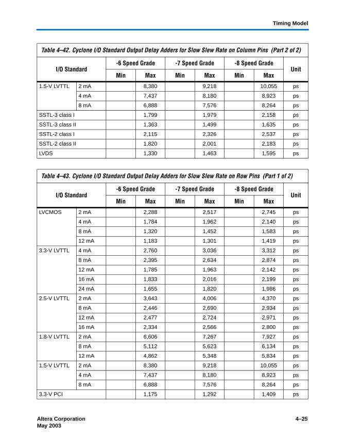
Altera Corporation 4–25May 2003 Preliminary
Timing Model
1.5-V LVTTL 2 mA 8,380 9,218 10,055 ps
4 mA 7,437 8,180 8,923 ps
8 mA 6,888 7,576 8,264 ps
SSTL-3 class I 1,799 1,979 2,158 ps
SSTL-3 class II 1,363 1,499 1,635 ps
SSTL-2 class I 2,115 2,326 2,537 ps
SSTL-2 class II 1,820 2,001 2,183 ps
LVDS 1,330 1,463 1,595 ps
Table 4–43. Cyclone I/O Standard Output Delay Adders for Slow Slew Rate on Row Pins (Part 1 of 2)
I/O Standard-6 Speed Grade -7 Speed Grade -8 Speed Grade
UnitMin Max Min Max Min Max
LVCMOS 2 mA 2,288 2,517 2,745 ps
4 mA 1,784 1,962 2,140 ps
8 mA 1,320 1,452 1,583 ps
12 mA 1,183 1,301 1,419 ps
3.3-V LVTTL 4 mA 2,760 3,036 3,312 ps
8 mA 2,395 2,634 2,874 ps
12 mA 1,785 1,963 2,142 ps
16 mA 1,833 2,016 2,199 ps
24 mA 1,655 1,820 1,986 ps
2.5-V LVTTL 2 mA 3,643 4,006 4,370 ps
8 mA 2,446 2,690 2,934 ps
12 mA 2,477 2,724 2,971 ps
16 mA 2,334 2,566 2,800 ps
1.8-V LVTTL 2 mA 6,606 7,267 7,927 ps
8 mA 5,112 5,623 6,134 ps
12 mA 4,862 5,348 5,834 ps
1.5-V LVTTL 2 mA 8,380 9,218 10,055 ps
4 mA 7,437 8,180 8,923 ps
8 mA 6,888 7,576 8,264 ps
3.3-V PCI 1,175 1,292 1,409 ps
Table 4–42. Cyclone I/O Standard Output Delay Adders for Slow Slew Rate on Column Pins (Part 2 of 2)
I/O Standard-6 Speed Grade -7 Speed Grade -8 Speed Grade
UnitMin Max Min Max Min Max

4–26 Altera CorporationPreliminary May 2003
Cyclone Device Handbook, Volume 1
Table 4–44 shows the adder delays for the IOE programmable delays. These delays are controlled with the Quartus II software options listed in the Parameter column.
SSTL-3 class I 1,799 1,979 2,158 ps
SSTL-3 class II 1,363 1,499 1,635 ps
SSTL-2 class I 2,115 2,326 2,537 ps
SSTL-2 class II 1,820 2,001 2,183 ps
LVDS 1,330 1,463 1,595 ps
Note to Tables 4–38 through 4–43:(1) EP1C3 devices do not support the PCI I/O standard.
Table 4–43. Cyclone I/O Standard Output Delay Adders for Slow Slew Rate on Row Pins (Part 2 of 2)
I/O Standard-6 Speed Grade -7 Speed Grade -8 Speed Grade
UnitMin Max Min Max Min Max
Table 4–44. Cyclone IOE Programmable Delays on Column Pins
Parameter Setting-6 Speed Grade -7 Speed Grade -8 Speed Grade
UnitMin Max Min Max Min Max
Decrease input delay to internal cells
On 3,057 3,362 3,668 ps
Small 2,212 2,433 2,654 ps
Medium 2,639 2,902 3,166 ps
Large 3,057 3,362 3,668 ps
Decrease input delay to input register
On 3,057 3,362 3,668 ps
Increase delay to output pin
On 552 607 662 ps

Altera Corporation 4–27May 2003 Preliminary
Timing Model
Maximum Input & Output Clock Rates
Tables 4–46 and 4–47 show the maximum input clock rate for column and row pins in Cyclone devices.
Table 4–45. Cyclone IOE Programmable Delays on Row Pins
Parameter Setting-6 Speed Grade -7 Speed Grade -8 Speed Grade
UnitMin Max Min Max Min Max
Decrease input delay to internal cells
On 3,057 3,362 3,668 ps
Small 2,212 2,433 2,654 ps
Medium 2,639 2,902 3,166 ps
Large 3,057 3,362 3,668 ps
Decrease input delay to input register
On 3,057 3,362 3,668 ps
Increase delay to output pin
On 556 611 667 ps
Table 4–46. Cyclone Maximum Input Clock Rate for Column Pins
I/O Standard -6 Speed Grade
-7 Speed Grade
-8 Speed Grade Unit
LVTTL 304 304 304 MHz
2.5 V 220 220 220 MHz
1.8 V 213 213 213 MHz
1.5 V 166 166 166 MHz
LVCMOS 304 304 304 MHz
SSTL-3 class I 100 100 100 MHz
SSTL-3 class II 100 100 100 MHz
SSTL-2 class I 134 134 134 MHz
SSTL-2 class II 134 134 134 MHz
LVDS 231 231 231 MHz
Table 4–47. Cyclone Maximum Input Clock Rate for Row Pins (Part 1 of 2)
I/O Standard -6 Speed Grade
-7 Speed Grade
-8 Speed Grade Unit
LVTTL 304 304 304 MHz
2.5 V 220 220 220 MHz
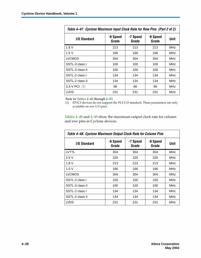
4–28 Altera CorporationPreliminary May 2003
Cyclone Device Handbook, Volume 1
Tables 4–48 and 4–49 show the maximum output clock rate for column and row pins in Cyclone devices.
1.8 V 213 213 213 MHz
1.5 V 166 166 166 MHz
LVCMOS 304 304 304 MHz
SSTL-3 class I 100 100 100 MHz
SSTL-3 class II 100 100 100 MHz
SSTL-2 class I 134 134 134 MHz
SSTL-2 class II 134 134 134 MHz
3.3-V PCI (1) 66 66 66 MHz
LVDS 231 231 231 MHz
Note to Tables 4–46 thorugh 4–47:(1) EP1C3 devices do not support the PCI I/O standard. These parameters are only
available on row I/O pins.
Table 4–48. Cyclone Maximum Output Clock Rate for Column Pins
I/O Standard -6 Speed Grade
-7 Speed Grade
-8 Speed Grade Unit
LVTTL 304 304 304 MHz
2.5 V 220 220 220 MHz
1.8 V 213 213 213 MHz
1.5 V 166 166 166 MHz
LVCMOS 304 304 304 MHz
SSTL-3 class I 100 100 100 MHz
SSTL-3 class II 100 100 100 MHz
SSTL-2 class I 134 134 134 MHz
SSTL-2 class II 134 134 134 MHz
LVDS 231 231 231 MHz
Table 4–47. Cyclone Maximum Input Clock Rate for Row Pins (Part 2 of 2)
I/O Standard -6 Speed Grade
-7 Speed Grade
-8 Speed Grade Unit

Altera Corporation 4–29May 2003 Preliminary
Timing Model
Table 4–49. Cyclone Maximum Output Clock Rate for Row Pins
I/O Standard -6 Speed Grade
-7 Speed Grade
-8 Speed Grade Unit
LVTTL 304 304 304 MHz
2.5 V 220 220 220 MHz
1.8 V 213 213 213 MHz
1.5 V 166 166 166 MHz
LVCMOS 304 304 304 MHz
SSTL-3 class I 100 100 100 MHz
SSTL-3 class II 100 100 100 MHz
SSTL-2 class I 134 134 134 MHz
SSTL-2 class II 134 134 134 MHz
3.3-V PCI (1) 66 66 66 MHz
LVDS 231 231 231 MHz
Note to Tables 4–48 through 4–49:(1) EP1C3 devices do not support the PCI I/O standard. These parameters are only
available on row I/O pins.

4–30 Altera CorporationPreliminary May 2003
Cyclone Device Handbook, Volume 1

Altera Corporation 5–1May 2003 Preliminary
5. Reference & OrderingInformation
Software Cyclone devices are supported by the Altera Quartus ® II design software, which provides a comprehensive environment for system-on-a-programmable-chip (SOPC) design. The Quartus ® II software includes HDL and schematic design entry, compilation and logic synthesis, full simulation and advanced timing analysis, SignalTap II logic analysis, and device configuration. See the Design Software Selector Guide for more details on the Quartus ® II software features.
The Quartus ® II software supports the Windows 2000/NT/98, Sun Solaris, Linux Red Hat v7.1 and HP-UX operating systems. It also supports seamless integration with industry-leading EDA tools through the NativeLink® interface.
Device Pin-Outs Device pin-outs for Cyclone devices are available on the Altera web site (www.altera.com) and in the Cyclone FPGA Device Handbook.
Ordering Information
Figure 5–1 describes the ordering codes for Cyclone devices. For more information on a specific package, refer to Chapter 6, Package Information for Cyclone Devices.
Figure 5–1. Cyclone Device Packaging Ordering Information
Device Type
Package Type
6, 7, or 8 , with 6 being the fastest
Number of pins for a particular package
ES:
T:Q:F:
Thin quad flat pack (TQFP)Plastic quad flat pack (PQFP)FineLine BGA
EP1C: Cyclone
3461220
C:I:
Commercial temperature (tJ = 0˚ C to 85˚ C)Industrial temperature (tJ = -40˚ C to 100˚ C)
Optional SuffixFamily Signature
Operating Temperature
Speed Grade
Pin Count
Engineering sample
7EP1C 20 C400F ES
Indicates specific device options or shipment method.
C51005-1.0

5–2 Altera CorporationPreliminary May 2003
Cyclone Device Handbook, Volume 1

Altera Corporation Section II–1Preliminary
Section II. ClockManagement
This section provides information on the Cyclone phase-lock loops (PLLs). The PLLs assist designers in managing clocks internally and also have the ability to drive off chip to control system-level clock networks. This chapter contains detailed information on the features, the interconnections to the logic array and off chip, and the specifications for Cyclone PLLs.
This section contains the following:
Chapter 6. Using PLLs in Cyclone Devices
Revision History The table below shows the revision history for Chapter 6.
Chapter(s) Date / Version Changes Made
6 May 2003v1.0
Revised Table 6–1 with EP1C4.Updated Figure 6–8 and added information to Table 6–9 for fIN and fOUT.

Section II–2 Altera CorporationPreliminary
Clock Management Cyclone Device Handbook, Volume 1

Altera Corporation 6–1May 2003 Preliminary
6. Using PLLs inCyclone Devices
Introduction CycloneTM FPGAs offer phase locked loops (PLLs) and a global clock network for clock management solutions. Cyclone PLLs offer clock multiplication and division, phase shifting, programmable duty cycle, and external clock outputs, allowing system-level clock management and skew control. The Altera® Quartus® II software enables Cyclone PLLs and their features without using any external devices. This application note explains how to design and enable Cyclone PLL features.
PLLs are commonly used to synchronize internal device clocks with an external clock, run internal clocks at higher frequencies than an external clock, minimize clock delay and clock skew, and reduce or adjust clock-to-out (TCO) and set-up (TSU) times.
Hardware Overview
Cyclone FPGAs contain up to two PLLs per device. Table 6–1 shows which PLLs are available for each Cyclone FPGA.
Table 6–1. Cyclone FPGA PLL Availability
Device PLL1 (1) PLL2 (2)
EP1C3 v
EP1C4 v v
EP1C6 v v
EP1C12 v v
EP1C20 v v
Notes to Table 6–1:(1) Located on the center left side of the device.(2) Located on the center right side of the device.
C51006-1.0

6–2 Altera CorporationPreliminary May 2003
Cyclone Device Handbook, Volume 1
Table 6–2 provides an overview of available Cyclone PLL features.
Cyclone PLL Blocks
The main goal of a PLL is to synchronize the phase and frequency of an internal/external clock to an input reference clock. There are a number of components that comprise a PLL to achieve this phase alignment.
Cyclone PLLs align the rising edge of the reference input clock to a feedback clock using a phase-frequency detector (PFD). The falling edges are determined by the duty cycle specifications. The PFD produces an up or down signal that determines whether the VCO needs to operate at a higher or lower frequency. The PFD output is applied to the charge pump and loop filter, which produces a control voltage for setting the frequency of the VCO. If the PFD produces an up signal, then the VCO frequency increases, while a down signal causes the VCO frequency to decrease.
The PFD outputs these up and down signals to a charge pump. If the charge pump receives an up signal, current is driven into the loop filter. Conversely, if it receives a down signal, current is drawn from the loop filter. The loop filter converts these up and down signals to a voltage that
Table 6–2. Cyclone PLL Features
Feature Description
Clock multiplication and division M/(N×post-scale counter) (1)
Phase shift Down to 156-pico second (ps) increments (2), (3)
Programmable duty cycle v
Number of internal clock outputs Two per PLL
Number of external clock outputs (4) One per PLL
Locked port can feed logic array v
PLL clock outputs can feed logic array v
Notes to Table 6–2:(1) M counter values range from 2 to 32. N and post-scale counter values range from
1 to 32.(2) The smallest phase shift is determined by the Voltage Control Oscillator (VCO)
period divided by 8.(3) For degree increments, Cyclone FPGAs can shift output frequencies in increments
of at least 45°. Smaller degree increments are possible depending on the multiplication/division ratio needed on the PLL clock output.
(4) The EP1C3 device in the 100-pin thin quad flat pack (TQFP) package does not have support for a PLL LVDS input or an external clock output. The EP1C6 PLL2 in the 144-pin TQFP package does not support an external clock output.

Altera Corporation 6–3May 2003 Preliminary
Introduction
is used to bias the VCO. The loop filter also removes glitches from the charge pump and prevents voltage over-shoot, which minimizes the jitter on the VCO.
The voltage from the loop filter determines how fast the VCO operates. The VCO is implemented as a four-stage differential ring oscillator. A divide counter (M) is inserted in the feedback loop to increase the VCO frequency above the input reference frequency, making the VCO frequency (fVCO) equal to M times the input reference clock (fREF). The input reference clock (fREF) to the PFD is equal to the input clock (fIN) divided by the pre-scale counter (N). Therefore, the feedback clock (fFB) that is applied to one input of the PFD is locked to the fREF that is applied to the other input of the PFD.
The VCO output can feed up to three post-scale counters (G0, G1, and E). These post-scale counters allow a number of harmonically-related frequencies to be produced within the PLL.
Additionally, the PLL has internal delay elements to compensate for routing on the global clock networks and I/O buffers of the external clock output pins. These internal delays are fixed and not accessible to the user.
Figure 6–1 shows a block diagram of the major components of a Cyclone PLL.
Figure 6–1. Cyclone PLL
Notes to Figure 6–1:(1) The EP1C3 device in the 100-pin TQFP package does not have support for a PLL LVDS input. (2) If you are using the LVDS standard, then both CLK pins of that PLL are used. LVDS input is supported via the
secondary function of the dedicated CLK pins. For PLL1, the CLK0 pin’s secondary function is LVDSCLK1p and the CLK1 pin’s secondary function is LVDSCLK1n. For PLL2, the CLK2 pin’s secondary function is LVDSCLK2p and the CLK3 pin’s secondary function is LVDSCLK2n.
(3) The EP1C3 device in the 100-pin TQFP package, and the EP1C6 PLL2 in the 144-pin TQFP package do not support an external clock output.
- VCO8
CLK(n)
PFD
VCO Phase SelectionSelectable at each PLL
Output Port
CLK(n+1)
LVDSCLK1n (1), (2)
÷ e
÷ g1
÷ g0
I/O Buffer (3)
Global Clock
Global Clock
Post-Scale Counters
Phase Frequency Detector
÷ m
LoopFilter
ChargePump
÷ n
fIN fREF
fFB
fVCO
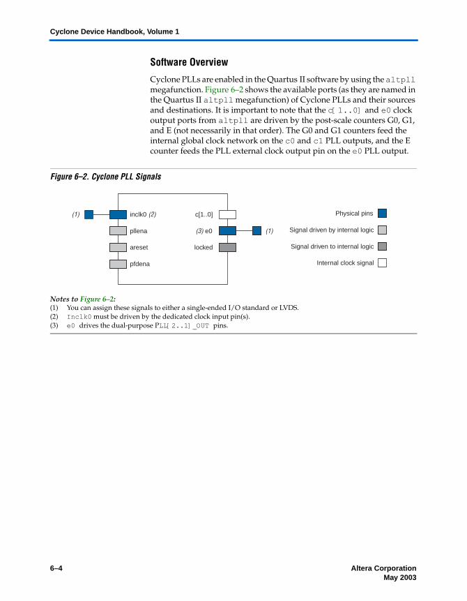
6–4 Altera CorporationPreliminary May 2003
Cyclone Device Handbook, Volume 1
Software Overview
Cyclone PLLs are enabled in the Quartus II software by using the altpll megafunction. Figure 6–2 shows the available ports (as they are named in the Quartus II altpll megafunction) of Cyclone PLLs and their sources and destinations. It is important to note that the c[1..0] and e0 clock output ports from altpll are driven by the post-scale counters G0, G1, and E (not necessarily in that order). The G0 and G1 counters feed the internal global clock network on the c0 and c1 PLL outputs, and the E counter feeds the PLL external clock output pin on the e0 PLL output.
Figure 6–2. Cyclone PLL Signals
Notes to Figure 6–2:(1) You can assign these signals to either a single-ended I/O standard or LVDS.(2) Inclk0 must be driven by the dedicated clock input pin(s).(3) e0 drives the dual-purpose PLL[2..1]_OUT pins.
inclk0 (2)
pllena
areset
pfdena
locked
c[1..0]
(3) e0
Internal clock signal
Signal driven by internal logic
Physical pins
Signal driven to internal logic
(1)
(1)
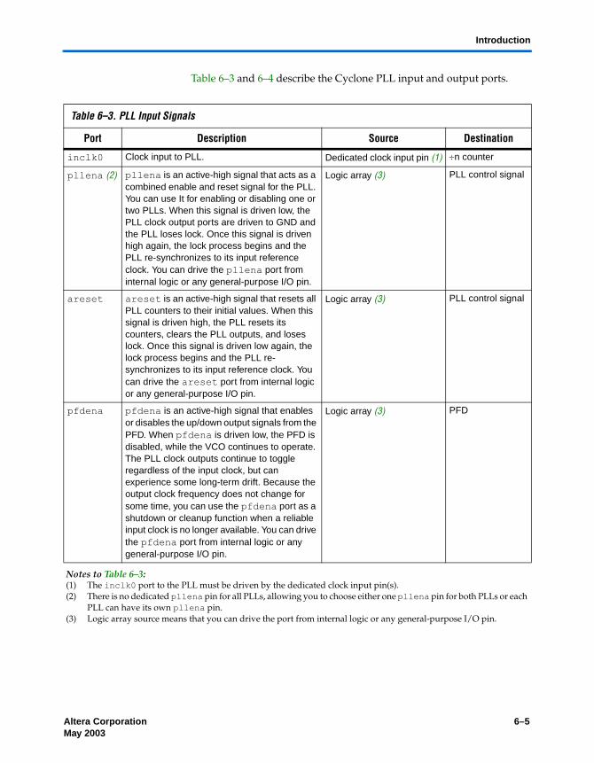
Altera Corporation 6–5May 2003 Preliminary
Introduction
Table 6–3 and 6–4 describe the Cyclone PLL input and output ports.
Table 6–3. PLL Input Signals
Port Description Source Destination
inclk0 Clock input to PLL. Dedicated clock input pin (1) ÷n counter
pllena (2) pllena is an active-high signal that acts as a combined enable and reset signal for the PLL. You can use It for enabling or disabling one or two PLLs. When this signal is driven low, the PLL clock output ports are driven to GND and the PLL loses lock. Once this signal is driven high again, the lock process begins and the PLL re-synchronizes to its input reference clock. You can drive the pllena port from internal logic or any general-purpose I/O pin.
Logic array (3) PLL control signal
areset areset is an active-high signal that resets all PLL counters to their initial values. When this signal is driven high, the PLL resets its counters, clears the PLL outputs, and loses lock. Once this signal is driven low again, the lock process begins and the PLL re-synchronizes to its input reference clock. You can drive the areset port from internal logic or any general-purpose I/O pin.
Logic array (3) PLL control signal
pfdena pfdena is an active-high signal that enables or disables the up/down output signals from the PFD. When pfdena is driven low, the PFD is disabled, while the VCO continues to operate. The PLL clock outputs continue to toggle regardless of the input clock, but can experience some long-term drift. Because the output clock frequency does not change for some time, you can use the pfdena port as a shutdown or cleanup function when a reliable input clock is no longer available. You can drive the pfdena port from internal logic or any general-purpose I/O pin.
Logic array (3) PFD
Notes to Table 6–3:(1) The inclk0 port to the PLL must be driven by the dedicated clock input pin(s).(2) There is no dedicated pllena pin for all PLLs, allowing you to choose either one pllena pin for both PLLs or each
PLL can have its own pllena pin. (3) Logic array source means that you can drive the port from internal logic or any general-purpose I/O pin.

6–6 Altera CorporationPreliminary May 2003
Cyclone Device Handbook, Volume 1
In the Quartus II software, you define which internal clock output from the PLL (c0 or c1) should be compensated. This PLL clock output is phase-aligned with respect to the PLL input clock. For example, if c0 is specified as the compensation clock in normal mode, the compensation is based on the c0 routing on the global clock network.
Pins & Clock Network Connections
You must drive Cyclone PLLs by the dedicated clock input pins CLK[3..0]. Inverted clocks and internally generated clocks cannot drive the PLL. Table 6–5 shows which dedicated clock pin drives which PLL input clock port.
Table 6–4. PLL Output Signals
Port Description Source Destination
c[1..0] PLL clock outputs driving the internal global clock network.
PLL post-scale counter G0 or G1 Global clock network (1)
e0 (2) PLL clock output driving the single-ended or LVDS external clock output pin(s).
PLL post-scale counter E PLL[2..1]_OUT pin(s) (3)
locked Gives the status of the PLL lock. When the PLL is locked, this port drives logic high. When the PLL is out of lock, this port drives logic low. The locked port can pulse high and low during the PLL lock process.
PLL lock detect Logic array (4)
Notes to Table 6–4:(1) C[1..0] can also drive to any general-purpose I/O pin through the global clock network.(2) The EP1C3 device in the 100-pin TQFP package, and the EP1C6 PLL2 in the 144-pin TQFP package do not have
support for the external clock output PLL[2..1]_OUT. (3) The PLL[2..1]_OUT pins are dual-purpose pins. If these pins are not required, they are available for use as
general-purpose I/O pins.(4) Logic array destination means that you can drive the port to internal logic or any general-purpose I/O pin.

Altera Corporation 6–7May 2003 Preliminary
Introduction
1 A single clock input pin cannot drive both PLLs, but a single clock input pin can feed both registers in the logic array, as well as the PLL inclk port.
The c[1..0] and e0 clock output ports from altpll are driven by the PLL post-scale counters G0, G1, and E (not necessarily in that order). The G0 and G1 counters feed the internal global clock network on the c0 and c1 PLL outputs, and the E counter feeds the PLL external clock output pin on the e0 PLL output. Table 6–6 shows which global clock network can be driven by which PLL post-scale counter output.
Figure 6–3 summarizes Table 6–5 and 6–6 by showing the PLL input and output clock connections.
Table 6–5. PLL Input Clock Sources
Clock Input Pins (1) PLL1 PLL2 (2)
CLK0 v
CLK1 v
CLK2 v
CLK3 v
Notes to Table 6–5:(1) If you are using the LVDS standard, then both CLK pins driving that PLL are used. (2) The EP1C3 device only supports PLL1.
Table 6–6. PLL Output Clock Destinations onto the Global Clock Network
PLL Counter Output GCLK0 GCLK1 GCLK2 GCLK3 GCLK4 GCLK5 GCLK6 GCLK7
PLL 1 G0 v v
G1 v v
PLL2 G0 v v
G1 v v

6–8 Altera CorporationPreliminary May 2003
Cyclone Device Handbook, Volume 1
Figure 6–3. Cyclone PLL Clock Connections
Notes to Figure 6–3:(1) PLL1 supports one single-ended or LVDS input via the CLK0 and CLK1 pins.(2) PLL2 supports one single-ended or LVDS input via the CLK2 and CLK3 pins.(3) PLL1_OUT and PLL2_OUT support single-ended or LVDS outputs. If the external clock output is not required, these
pins are available as general-purpose I/O pins.
You can invert the clock outputs of the PLL at the logic array block (LAB) and at the input/output element (IOE) level.
Hardware Features
Cyclone PLLs have a number of advanced features available, including clock multiplication and division, phase shifting, programmable duty cycles, external clock outputs, and control signals.
Clock Multiplication & Division
Cyclone PLLs provide clock synthesis for PLL output ports using M/(N × post-scale) scaling factors. There is one pre-scale divider (N) and one multiply counter (M) per PLL. M counter values range from 2 to 32. N and post-scale counter values range from 1 to 32. The input clock (fIN) is divided by a pre-scale counter (N) to produce the input reference clock (fREF) to the PFD. fREF is then multiplied by the M feedback factor. The control loop drives the VCO frequency to match fIN × (M/N). See the following equations:
fREF = fIN/N
fVCO = fREF × M = fIN × (M/N)
CLK2
CLK3 (2)
PLL 2
G0
G1
E
CLK0
(1) CLK1
PLL 1
G0
G1
E
GCLK0
GCLK1
GCLK2
GCLK3 GCLK7
GCLK6
GCLK5
GCLK4
Global Clocks
(3) PLL1_OUT PLL2_OUT (3)

Altera Corporation 6–9May 2003 Preliminary
Hardware Features
Each output port has a unique post-scale counter to divide down the high-frequency VCO. There are three post-scale counters (G0, G1, and E) that range from 1 to 32. See the following equations:
fC0 = fVCO/G0 = fIN × (M/(N × G0))fC1 = fVCO/G1 = fIN × (M/(N × G1))fE = fVCO/E = fIN × (M/(N × E))
1 c0 and c1 can use either post-scale counter, G0 or G1.
For multiple PLL outputs with different frequencies, the VCO is set to the least common multiple of the output frequencies that meets the VCO frequency specifications. Then, the post-scale counters scale down the output frequency for each PLL clock output port. For example, if clock output frequencies required from one PLL are 33 and 66 MHz, the VCO is set to 330 MHz (the least common multiple in the VCO’s range).
Phase Shifting
Cyclone PLLs have advanced clock shift capability to provide programmable phase shifting. You can enter the desired phase shift in the altpll MegaWizard® Plug-In Manager and the Quartus II software automatically sets and displays the closest phase shift achievable. You can enter the phase shift in degrees, or units of time, for each PLL clock output port. This feature is supported on all three PLL post-scale counters, G0, G1, and E and is supported for all available clock feedback modes.
Phase shifting is performed with respect to the PLL clock output that is compensated. For example, you have a 100 MHz input clock and request a × 1 multiplication with a +90° phase shift on c0 and a × 1 multiplication with a +45° phase shift on c1. If you choose to compensate for the c0 clock output, the PLL uses a zero phase-shifted c0 clock as a reference point to produce the +90° phase shift on c0. Since c0 is the compensated clock, it is phase-shifted +90° from the input clock. The c1 clock also uses the zero phase-shifted c0 reference to produce the +45° phase shift on c1.
For fine phase adjustment, each PLL clock output counter can choose a different phase of the VCO from up to eight phase taps. In addition, each clock output counter can use a unique initial count setting to achieve individual coarse phase shift selection, in steps of one VCO period. The Quartus II software can use this clock output counter, along with an initial setting on the post-scale counter, to achieve a phase shift range for the entire period of the output clock. You can phase shift the PLL clock output up to ±180°. The Quartus II software automatically sets the phase taps and counter settings according to the phase shift requested.

6–10 Altera CorporationPreliminary May 2003
Cyclone Device Handbook, Volume 1
The resolution of the fine phase adjustment is dependent on the input frequency and the multiplication/division factors (i.e., it is a function of the VCO period), with the finest step being equal to an eighth ( × 0.125) of the VCO period. The minimum phase shift is 1/(8 × fVCO) or N/(8 × M × fIN). In Cyclone FPGAs, the VCO ranges from 300 to 800 MHz. Therefore, phase shifting can be performed with a resolution range of 1/(8 × 800 MHz) to 1/(8 × 300 MHz), which is 156 to 417 ps in time units.
Because there are eight VCO phase taps, the maximum step size is 45°. Smaller steps are possible, depending on the multiplication and division ratio necessary on the output clock port. The equation to determine the precision of the phase shifting in degrees is 45° divided by the post-scale counter value. For example, if you have an input clock of 125 MHz with × 1, the post-scale counter G0 is 3. Therefore, the smallest phase shift step is (45°/3 = 15°) and possible phase-shift values would be multiples of 15°.
This type of phase shift provides the highest precision since it is the least sensitive to process, voltage and temperature variation.
Programmable Duty Cycle
The programmable duty cycle feature allows you to set the duty cycle of the PLL clock outputs. The duty cycle is the ratio of the clock output high/low time to the total clock cycle time, which is expressed as a percentage of high time. This feature is supported on all three PLL post-scale counters (G0, G1, and E).
The duty cycle is set by using a low- and high-time count setting for the post-scale counters. The Quartus II software uses the input frequency and target multiply/divide ratio to select the post-scale counter. The precision of the duty cycle is determined by the post-scale counter value chosen on a PLL clock output and is defined as 50% divided by the post-scale counter value. For example, if the post-scale counter value is 3, the allowed duty cycle precision would be 50% divided by 3 equaling 16.67%. Because the altpll megafunction does not accept non-integer values for the duty cycle values, the allowed duty cycles are 17, 33, 50, and 67%.
Due to hard limitations, you cannot achieve a duty cycle of 84% because you cannot achieve the closest value to 100% for a given counter value. However, you can achieve a duty cycle of 84% by choosing a 17% duty cycle and inverting the PLL clock output. For example, if the G0 counter is 10, increments of 5% are possible for duty cycle choices between 5 and 90%.
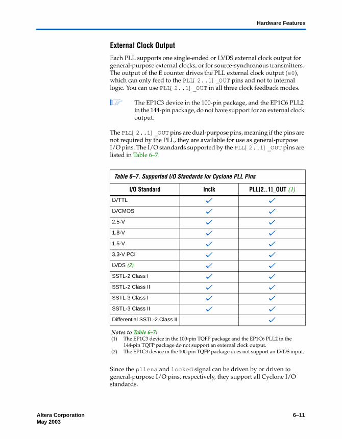
Altera Corporation 6–11May 2003 Preliminary
Hardware Features
External Clock Output
Each PLL supports one single-ended or LVDS external clock output for general-purpose external clocks, or for source-synchronous transmitters. The output of the E counter drives the PLL external clock output (e0), which can only feed to the PLL[2..1]_OUT pins and not to internal logic. You can use PLL[2..1]_OUT in all three clock feedback modes.
1 The EP1C3 device in the 100-pin package, and the EP1C6 PLL2 in the 144-pin package, do not have support for an external clock output.
The PLL[2..1]_OUT pins are dual-purpose pins, meaning if the pins are not required by the PLL, they are available for use as general-purpose I/O pins. The I/O standards supported by the PLL[2..1]_OUT pins are listed in Table 6–7.
Since the pllena and locked signal can be driven by or driven to general-purpose I/O pins, respectively, they support all Cyclone I/O standards.
Table 6–7. Supported I/O Standards for Cyclone PLL Pins
I/O Standard Inclk PLL[2..1]_OUT (1)
LVTTL v v
LVCMOS v v
2.5-V v v
1.8-V v v
1.5-V v v
3.3-V PCI v v
LVDS (2) v v
SSTL-2 Class I v v
SSTL-2 Class II v v
SSTL-3 Class I v v
SSTL-3 Class II v v
Differential SSTL-2 Class II v
Notes to Table 6–7:(1) The EP1C3 device in the 100-pin TQFP package and the EP1C6 PLL2 in the
144-pin TQFP package do not support an external clock output.(2) The EP1C3 device in the 100-pin TQFP package does not support an LVDS input.

6–12 Altera CorporationPreliminary May 2003
Cyclone Device Handbook, Volume 1
The Cyclone external clock output pins (PLL[2..1]_OUT) do not have a separate VCC and GND bank internal to the device. The PLL[2..1]_OUT pins share a VCCIO bank with neighboring I/O pins. Only the I/O pins in the same bank have an effect on the PLL[2..1]_OUT pins. Therefore, to minimize jitter on the PLL[2..1]_OUT pins, I/O pins directly adjacent to these pins should be either inputs or they should not be used. For more information about board design guidelines, see “Jitter Considerations” on page 6–19.
Control Signals
There are four available control signals, pllena, areset, pfdena, and locked, in Cyclone PLLs that provide added PLL management.
pllena
The PLL enable signal, pllena, enables or disables the PLL. When pllena is low, the PLL clock output ports are driven to logic low and the PLL loses lock. When pllena goes high again, the PLL relocks and resynchronizes to the input clock. Therefore, pllena is an active-high signal. In Cyclone FPGAs, you can feed the pllena port from internal logic or any general-purpose I/O pin because there is no dedicated pllena pin. This feature offers added flexibility, since each PLL can have its own pllena control circuitry, or both PLLs can share the same pllena circuitry. The pllena signal is optional, and when it is not enabled in the software, the port is internally tied to VCC.
areset
The PLL areset signal is the reset or resynchronization input for each PLL. When driven high, the PLL counters reset, clearing the PLL output and causing the PLL to lose lock. The VCO resets back to its nominal setting. When areset is again driven low, the PLL resynchronizes to its input clock as the PLL re-locks. If the target VCO frequency is below this nominal frequency, the PLL clock output frequency begins at a higher value than desired during the lock process. areset is an active-high signal. Cyclone FPGAs can drive this PLL input signal from internal logic or any general-purpose I/O pin. The areset signal is optional, and when it is not enabled in the software, the port is internally tied to GND.
pfdena
The pfdena signal controls the PFD output in the PLL with a programmable gate. If you disable the PFD by driving areset low, the VCO operates at its last set control voltage and frequency value with some long-term drift to a lower frequency. The VCO frequency can drift up to +/- 5% over 25 us. Even though the PLL clock outputs continue to

Altera Corporation 6–13May 2003 Preliminary
Clock Feedback Modes
toggle regardless of the input clock, the PLL could lose lock. The system continues running when the PLL goes out of lock, or if the input clock is disabled. Because the last locked output frequency does not change for some time, you can use the pfdena port as a shutdown or cleanup function when a reliable input clock is no longer available. By maintaining this frequency, the system has time to store its current settings before shutting down. If the pfdena signal goes high again, the PLL relocks and resynchronizes to the input clock. Therefore, the pfdena pin is an active-high signal. You can drive the pfdena input signal by any general-purpose I/O pin, or from internal logic. This signal is optional, and when it is not enabled in the software, the port is internally tied to VCC.
locked
When the locked output is at a logic-high level, this level indicates a stable PLL clock output in phase with the PLL reference input clock. Without any additional circuitry, the locked port may toggle as the PLL begins tracking the reference clock. The locked port of the PLL can feed any general-purpose I/O pin and/or internal logic. This locked signal is optional, but is useful in monitoring the PLL lock process.
Clock Feedback Modes
Cyclone PLLs support three feedback modes: normal, zero delay buffer, and no compensation. Unlike other Altera device families, Cyclone PLLs do not have support for external feedback mode. All three supported clock feedback modes allow for multiplication/division, phase shifting, and programmable duty cycle. The following sections give a brief description of each mode.
1 The phase relationship shown in Figure 6–4 through 6–6 are for the default phase shift setting of 0°. Changing the phase-shift setting will change the relationships.
Normal Mode
In normal mode, the PLL phase aligns the input reference clock with the clock signal at the ports of the registers in the logic array or the IOE to compensate for the internal global clock network delay. In the altpll MegaWizard Plug-In Manager, you can define which internal clock output from the PLL (c0 or c1) should be compensated.
If the external clock output (PLL[2..1]_OUT) is used in this mode, there will be a phase shift with respect to the clock input pin. Similarly, if you use the internal PLL clock outputs to drive general-purpose I/O pins, there will be a phase shift with respect to the clock input pin.

6–14 Altera CorporationPreliminary May 2003
Cyclone Device Handbook, Volume 1
Figure 6–4 shows an example waveform of the PLL clocks’ phase relationship in normal mode.
Figure 6–4. Phase Relationship Between PLL Clocks in Normal Mode
Note to Figure 6–4:(1) The external clock output can lead or lag the PLL clock signals.
Zero Delay Buffer Mode
The clock signal on the PLL external clock output pin (PLL[2..1]_OUT) is phase-aligned with the PLL input clock for zero delay. If you use the c[1..0] ports to drive internal clock ports, there will be a phase shift with respect to the input clock pin. Figure 6–5 shows an example waveform of the PLL clocks’ phase relationship in zero delay buffer mode.
PLL inclk
External PLL clock outputs (1)
PLL clock at the register clock port
Phase Aligned

Altera Corporation 6–15May 2003 Preliminary
Clock Feedback Modes
Figure 6–5. Phase Relationship Between PLL Clocks in Zero Delay Buffer Mode
No Compensation
In this mode, the PLL does not compensate for any clock networks, which leads to better jitter performance because the clock feedback into the PFD does not pass through as much circuitry. Both the PLL internal and external clock outputs are phase shifted with respect to the PLL clock input. Figure 6–6 shows an example waveform of the PLL clocks’ phase relationship in no compensation mode.
PLL inclk
External PLL clock outputs
PLL clock at theregister clock port
Phase Aligned

6–16 Altera CorporationPreliminary May 2003
Cyclone Device Handbook, Volume 1
Figure 6–6. Phase Relationship Between PLL Clocks in No Compensation Mode
Note to Figure 6–6:(1) Internal clocks fed by the PLL are in phase alignment with each other.
Pins Table 6–8 describes the Cyclone PLL-related physical pins and their functionality.
PLL inclk
External PLL clock outputs
PLL clock at theRegister clock port (1)
Phase Aligned
Table 6–8. Cyclone PLL Pins (Part 1 of 2)
Pin Name Description
CLK0 Single-ended or LVDS p-pin that can drive the inclk0 port of PLL1.
CLK1 (1) Single-ended or LVDS n-pin that can drive the inclk0 port of PLL1.
CLK2 Single-ended or LVDS p-pin that can drive the inclk0 port of PLL2.
CLK3 (1) Single-ended or LVDS n-pin that can drive the inclk0 port of PLL2.
PLL1_OUTp (2)PLL1_OUTn (2)
Single-ended or LVDS pins driven by the e0 port from PLL1. If not used by the PLL, these are available as general-purpose I/O pins.
PLL2_OUTp (2)PLL2_OUTn (2)
Single-ended or LVDS pins driven by the e0 port from PLL2. If not used by the PLL, these are available as general-purpose I/O pins.
VCCA_PLL1 (3) Analog power for PLL1. Even if the PLL is not used, you must connect this pin to 1.5 V.
GNDA_PLL1 (4) Analog ground for PLL1. You can connect this pin to the GND plane on the board.
VCCA_PLL2 (3) Analog power for PLL2. Even if the PLL is not used, you must connect this pin to 1.5 V.

Altera Corporation 6–17May 2003 Preliminary
Board Layout
Board Layout Cyclone PLLs contain analog components that are embedded in a digital device. These analog components have separate power and ground pins to provide immunity against noise generated by the digital components. These separate VCC and GND pins are used to isolate circuitry and improve noise resistance.
VCCA & GNDA
Each PLL has separate VCC and GND pairs for their analog circuitry. The analog circuit power and ground pin for each PLL is called VCCA_PLL# and GNDA_PLL# (# represents the PLL number). Even if the PLL is not used, the VCCA power must be connected to a 1.5-V supply. The power connected to VCCA must be isolated from the power to the rest of the Cyclone FPGA, or any other digital device on the board. The following sections describe three different methods for isolating VCCA.
Separate VCCA Power Plane
The designer of a mixed-signal system would have already partitioned the system into analog and digital sections, each with its own power planes on the board. In this case, you can connect VCCA to the analog 1.5-V power plane.
Partitioned VCCA Island within VCCINT Plane
Most systems using Altera devices are fully digital, so there is not a separate analog power plane readily available on the board. Adding new planes to the board may be expensive. Therefore, you can create islands
GNDA_PLL2 (4) Analog ground for PLL2. You can connect this pin to the GND plane on the board.
GNDG_PLL1 (5) Guard ring ground for PLL1. You can connect this pin to the GND plane on the board.
GNDG_PLL2 (5) Guard ring ground for PLL2. You can connect this pin to the GND plane on the board.
Notes to Table 6–8:(1) The EP1C3 device in the 100-pin TQFP package does not have dedicated clock pins CLK1 and CLK3.(2) The EP1C3 device in the 100-pin TQFP package, and the EP1C6 PLL2 in the 144-pin TQFP package do not support
an external clock output. (3) Refer to “Board Layout” on page 6–17 for filtering and other recommendations.(4) The EP1C3 device in the 100-pin TQFP package, and the EP1C6 PLL2 in the 144-pin TQFP package do not have a
separate GNDA_PLL pin. They are internally tied to GND. (5) The Guard ring power (VCCG_PLL) is tied internally to VCCINT.
Table 6–8. Cyclone PLL Pins (Part 2 of 2)
Pin Name Description
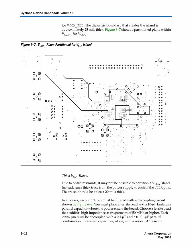
6–18 Altera CorporationPreliminary May 2003
Cyclone Device Handbook, Volume 1
for VCCA_PLL. The dielectric boundary that creates the island is approximately 25 mils thick. Figure 6–7 shows a partitioned plane within VCCINT for VCCA.
Figure 6–7. VCCINT Plane Partitioned for VCCA Island
Thick VCCA Traces
Due to board restraints, it may not be possible to partition a VCCA island. Instead, run a thick trace from the power supply to each of the VCCA pins. The traces should be at least 20 mils thick.
In all cases, each VCCA pin must be filtered with a decoupling circuit shown in Figure 6–8. You must place a ferrite bead and a 10-µF tantalum parallel capacitor where the power enters the board. Choose a ferrite bead that exhibits high impedance at frequencies of 50 MHz or higher. Each VCCA pin must be decoupled with a 0.1-µF and a 0.001-µF parallel combination of ceramic capacitors, along with a series 1-Ω resistor,

Altera Corporation 6–19May 2003 Preliminary
Board Layout
located as close as possible to the Cyclone FPGA. You can connect the GNDA pins directly to the same GND plane as the digital GND of the device.
Figure 6–8. PLL Power Schematic for Cyclone PLLs
f For more information about board design guidelines, see Application Note 75: High-Speed Board Design.
Jitter Considerations
If the input clocks have any low-frequency jitter (below the PLL bandwidth), the PLL attempts to track it, which increases the jitter seen at the PLL clock output. To minimize this effect, avoid placing noisy signals in the same VCCIO bank as those that power the PLL clock input buffer. This is only important if the PLL input clock is assigned to 3.3-V or 2.5-V LVTTL or LVCMOS I/O standards. With these I/O standards, VCCIO
Cyclone Device
1.5-V Supply
Ferrite Bead
10 µF
GND
Repeat for each PLL powerand ground set
GND GND
GND
PLL<#>_VCCA
PLL<#>_GNDA
PLL<#>_GNDG
-1 µF .001 µF

6–20 Altera CorporationPreliminary May 2003
Cyclone Device Handbook, Volume 1
powers the input clock buffer. Therefore, any noise on this VCCIO supply can affect jitter performance. For all other I/O standards the input buffers are powered by VCCINT.
Because Cyclone external clock output pins (PLL[2..1]_OUT) do not have a separate VCC and GND bank, you should avoid placing noisy output signals directly next to these pins. Therefore, Altera recommends that PLL[2..1]_OUT neighboring I/O pins should be either inputs pins or not used at all. If noisy outputs are placed next to the PLL[2..1]_OUT pins, they could inject noise through ground bounce or VCC sag and mutual pin inductance, which would result in worse jitter performance on the PLL[2..1]_OUT pins.
Additionally, you should take into consideration the number of simultaneously switching outputs within the same VCCIO bank as the PLL[2..1]_OUT pins. Altera recommends that you switch as few outputs simultaneously in the same direction as possible in these VCCIO banks. Also, if you have switching outputs in the same VCCIO bank as the PLL[2..1]_OUT pins, Altera recommends that you use the low current strength and/or slow slew rate options on those output pins as they will help to improve the jitter performance.
Specifications Table 6–9 describes the Cyclone FPGA PLL specifications.
Table 6–9. Cyclone PLL Specifications Note (1) (Part 1 of 2)
Symbol Parameter Min Max Unit
fIN(-6 speed grade) Input frequency 15.00 200 MHz
fIN(-7 speed grade) Input frequency 15.00 181 MHz
fIN(-8 speed grade) Input frequency 15.00 166 MHz
fIN DUTY Input clock duty cycle 40.00 60 %
tIN JITTER Input clock jitter (peak-to-peak) ± 200 ps
fOUT(-6 speed grade) PLL output frequency 9.38 312 MHz
fOUT(-7 speed grade) PLL output frequency 9.38 283 MHz
fOUT(-8 speed grade) PLL output frequency 9.38 260 MHz
tOUT DUTY Duty cycle for external clock output (when set to 50%)
45.00 55 %
tJITTER (2) PLL external clock output jitter (peak-to-peak)
TBD ps
tLOCK Time required to lock from end of device configuration
10.00 100 µs

Altera Corporation 6–21May 2003 Preliminary
Software Support
Software Support
Support for Cyclone PLLs is available in the Quartus II software by using the altpll megafunction. The following section describes how the altpll megafunction enables the various Cyclone PLL features and options. This section includes the megafunction symbol, the input and output ports, a description of the MegaWizard Plug-In Manager options, and example MegaWizard screen shots.
Quartus II altpll Megafunction
Figure 6–9 shows the altpll megafunction symbol in the Quartus II software.
Figure 6–9. altpll Megafunction Symbol Targeted for Cyclone FPGAs
fVCO PLL internal VCO operating range
300.00 800 MHz
M (3) Counter values 2 32 integer
N, G0, G1, E Counter values 1 32 integer
Notes to Table 6–9:(1) These numbers are preliminary and pending silicon characterization.(2) The tJITTER specification for the PLL[2..1]_OUT pins are dependent on the I/O pins in its VCCIO bank, how many
of them are switching outputs, how much they toggle, and whether or not they use programmable current strength or slow slew rate.
(3) M can only range from 2 - 32 because the maximum PLL input frequency is 200 MHz and the minimum VCO frequency is 300 MHz. Since fVCO = fIN × (M / N) there can never be a situation when M = 1 since that would violate the minimum VCO frequency specification.
Table 6–9. Cyclone PLL Specifications Note (1) (Part 2 of 2)
Symbol Parameter Min Max Unit

6–22 Altera CorporationPreliminary May 2003
Cyclone Device Handbook, Volume 1
f Refer to Quartus II Help for the altpll megafunction AHDL functional prototypes (applicable to Verilog HDL), VHDL component declaration, and parameter descriptions.
altpll Input Ports
Table 6–10 shows the input ports of the altpll megafunction and describes their function.
Table 6–10. Input Ports of the altpll Megafunction
Port Name Required Description
inclk0 (1) Yes The input clock port that drives the PLL.
pllena (2) No pllena is an active-high signal, which acts as a combined enable and reset signal for the PLL. You can use it for enabling or disabling one or both PLLs. When this signal is driven low, the PLL clock output ports are driven to GND and the PLL loses lock. Once this signal is driven high again, the lock process begins and the PLL re-synchronizes to its input reference clock. The pllena port can be driven from internal logic or any general-purpose I/O pin.
areset (2) No areset is an active-high signal, which resets all PLL counters to their initial values. When this signal is driven high, the PLL resets its counters, clears the PLL outputs, and loses lock. Once this signal is driven low again, the lock process begins and the PLL re-synchronizes to its input reference clock. You can drive the areset port from internal logic or any general-purpose I/O pin.
pfdena (2) No pfdena is an active-high signal, which enables or disables the up/down output signals from the PFD. When pfdena is driven low, the PFD is disabled, while the VCO continues to operate. PLL clock outputs continue to toggle regardless of the input clock, but can experience some long-term drift. Because the output clock frequency does not change for some time, you can use the pfdena port as a shutdown or cleanup function when a reliable input clock is no longer available. You can drive the pfdena port from internal logic or any general-purpose I/O pin.
Notes to Table 6–10:(1) The inclk0 port to the PLL must be driven by the dedicated clock input pin(s).(2) See “Control Signals” on page 6–12 for further details.

Altera Corporation 6–23May 2003 Preliminary
Software Support
altpll Output Ports
Table 6–11 shows the output ports of the altpll megafunction and describes their function.
MegaWizard Customization
You can use the MegaWizard Plug-In Manager to set the altpll megafunction options for each PLL instance in your design.
f If you instantiate the altpll megafunction without using the MegaWizard Plug-In Manager, search for “altpll” in the Quartus II Help for a list of the altpll parameters.
In the MegaWizard Plug-In Manager, select the altpll megafunction in the I/O directory from the Available Megafunctions dialog box (see Figure 6–10). The altclklock megafunction is also available from the Quartus II software for backward compatibility, but instantiates the new altpll megafunction when targeting Cyclone FPGAs.
Table 6–11. Output Ports of the altpll Megafunction
Port Name Required Description
c[1..0] (1) No Clock output of the PLL that drives the internal global clock network.
e0 (1) No Clock output that feeds the external clock output pins, PLL[2..1]_OUT.
locked (2) No Gives the status of the PLL lock. When the PLL is locked, this port drives logic high. When the PLL is out of lock, this port drives logic low. The locked port can pulse high and low during the PLL lock process.
Notes to Table 6–11:(1) Either the internal or external clock output of the PLL must be selected. (2) See “Control Signals” on page 6–12 for further details.

6–24 Altera CorporationPreliminary May 2003
Cyclone Device Handbook, Volume 1
Figure 6–10. altpll Megafunction Selection in the MegaWizard Plug-In Manager
The altpll MegaWizard Plug-In Manager has separate pages that apply to Cyclone PLLs. The MegaWizard will gray-out options that are unavailable in Cyclone PLLs. During compilation, the Quartus II Compiler verifies the altpll parameters selected against the available PLLs, and any PLL or input clock location assignments.
At the top right-hand corner of each page of the altpll MegaWizard Plug-In Manager, there is a jump to page drop-down list (see Figure 6–11). This drop-down list allows you to jump to any particular altpll MegaWizard page and set those options.

Altera Corporation 6–25May 2003 Preliminary
Software Support
Figure 6–11. Jump to Page Drop-Down List in the altpll MegaWizard Plug-In
MegaWizard Page Description
This section describes the options available on the altpll MegaWizard pages. Each of the MegaWizard pages are shown. Tables 6–12 through 6–14 describe the features or settings on that page that apply to Cyclone PLLs. Use these tables, along with the hardware descriptions of the PLL features, to determine appropriate settings for your PLL instance.
You can use the General/Modes (Page 1) of the altpll MegaWizard Plug-In Manager for selecting the target device family, clock input frequency, general control signal selection, and clock feedback operation mode (see Figure 6–12 and Table 6–12).

6–26 Altera CorporationPreliminary May 2003
Cyclone Device Handbook, Volume 1
Figure 6–12. altpll MegaWizard Plug-In Manager (Page 1)
Table 6–12. altpll MegaWizard Plug-In Options Page 1 (Part 1 of 2)
Function Description
Which device family will you be using?
This application note explains all altpll options that apply when Cyclone is the target device family selected.
What is the frequency of the inclock0 input
The frequency for the PLL input clock, inclock0.
Create an pllena input to selectively enable the PLL
Creates a pllena port for this PLL instance. See Table 6–10 for pllena port description.
Create an areset input to asynchronously reset the PLL
Creates a areset port for this PLL instance. See Table 6–10 for areset port description.
Create an pfdena input to selectively enable the PFD
Creates a pfdena port for this PLL instance. See Table 6–10 for pfdena port description.

Altera Corporation 6–27May 2003 Preliminary
Software Support
Use the feedback path inside the PLL
This option sets the OPERATION_MODE parameter to either normal, zero delay buffer, or no compensation mode. In normal mode, the PLL feedback path comes from a global clock network, which minimizes the clock delay to registers for that specific PLL clock output. You can specify which PLL output is compensated for by using the COMPENSATE_CLOCK parameter.In zero delay buffer mode, the PLL feedback path is confined to the dedicated PLL external output pin. The clock signal driven off-chip on the PLL_OUT pin is phase aligned with the PLL clock input for a minimized delay between clock input and external clock output. If the PLL is also used to drive the internal clock network, a corresponding phase shift of that clock network results.In no compensation mode, the PLL feedback path is confined to the PLL loop; it does not come from the global clock network or an external source. There is no clock network compensation, but this mode minimizes jitter on clocks. This mode may lead to positive hold times on IOE registers; you can use manual phase shifting to compensate for positive hold times.For more information, see “Clock Feedback Modes” on page 6–13.
Which output clock will be compensated?
Indicates which output port of the PLL is compensated. For normal mode, you can select c0 or c1.
Table 6–12. altpll MegaWizard Plug-In Options Page 1 (Part 2 of 2)
Function Description

6–28 Altera CorporationPreliminary May 2003
Cyclone Device Handbook, Volume 1
You can use Scan/Lock (Page 2) for selecting the locked output port (see Figure 6–13 and Table 6–13).
Figure 6–13. altpll MegaWizard Plug-In Manager (Page 2)
The options on the next two pages of the MegaWizard Plug-In Manager, (Pages 3 to 4, titled Bandwidth/SS and Clock Switchover) are not supported in Cyclone FPGAs.
Table 6–13. altpll MegaWizard Plug-In Options Page 2
Function Description
Create "locked" output Creates a locked output port to indicate PLL lock. See locked port description in Table 6–11.

Altera Corporation 6–29May 2003 Preliminary
Software Support
Figure 6–14. altpll MegaWizard Plug-In Manager Pages 5 of 8
The last 3 pages of the MegaWizard Plug-In Manager (Pages 5 to 7) allow you to set the multiplication/division factors, phase shift, and duty cycle for each PLL output port (see Figure 6–14 and Table 6–14).

6–30 Altera CorporationPreliminary May 2003
Cyclone Device Handbook, Volume 1
Each page represents the settings for one PLL clock output port. Table 6–14 describes the options for Pages 5 to 8.
Page 8 is the summary page and tells you what files the MegaWizard Plug-In Manager will create (see Figure 6–15).
Table 6–14. altpll MegaWizard Plug-In Options Pages 5 of 8
Function Description
Clock multiplication factor (ratio)
Specifies the clock multiplication for this PLL output. The multiplication factor cannot be greater than 32.
Clock division factor (ratio) Specifies the clock division for this PLL output.
Clock phase shift (Ph) Sets the programmable phase shift for the clock output with respect to the PLL clock output that is compensated. The equation to determine the precision of the phase shifting in degrees is (45° divided by the post-scale counter value). Therefore, the maximum step size is 45°, and smaller steps are possible, depending on the multiplication/division ratio necessary on the clock output port. For example, if you have an input clock of 125 MHz with ×1, the post-scale counter G0 is 3. Therefore, the smallest phase shift step is 15°, and additional phase shifting is in 15° increments.
The up/down buttons cycle through the possible phase shift settings with the default M and post-scale dividers that the MegaWizard Pug-In Manager has chosen for your target frequency and multiplication/division ratio. It is possible to get other granularities of phase shifts if you manually enter a number into the phase shift field. For example, you can override the MegaWizard-chosen values and manually enter 7.5°. The MegaWizard Plug-In Manager verifies this is possible by using M = 6 and G0 = 6. The MegaWizard Plug-In Manager tries to achieve the closest phase shift possible. For example, if you enter 10°, the MegaWizard Plug-In Manager verifies that 9° is possible by using M = 5 and G0 = 5.
For more information, see “Phase Shifting” on page 6–9.
Clock duty cycle (DC) Specifies the clock duty cycle of the PLL clock output.
The equation to determine the precision of the duty cycle is (50% divided by the post-scale counter value). For example, if post-scale counter G0 is 3, the allowed duty cycles are 50% divided by 3, equaling 16.67%. Because the altpll megafunction does not accept non-integer values for the duty cycle values, the allowed duty cycles are 17, 33, 50, and 67%. Due to hard limitations, a duty cycle of 84% cannot be achieved because the closest value to 100% cannot be achieved for a given counter value. However, you can achieve a duty cycle of 84% by choosing a 17% duty cycle and inverting the PLL clock output. Use the up/down buttons to cycle through all possible settings.
For more information, see “Programmable Duty Cycle” on page 6–10.

Altera Corporation 6–31May 2003 Preliminary
Software Support
1 You can click Finish at anytime while in the MegaWizard Plug-In Manager to update the files.
Figure 6–15. altpll MegaWizard Plug-In Manager Page 8
Compilation Report
During compilation, an information message displays whether the requested multiplication/division factors, and/or phase shift, and/or duty cycle were achieved. If you enter an invalid multiplication/division ratio, compilation fails, and the Quartus II software displays an error message. If you enter an invalid phase shift or duty cycle value, the compilation proceeds, and you will receive an information message displaying the best alternative values chosen by the Quartus II software.
The Resource Section of the compilation report provides two PLL reports: the PLL Summary and the PLL Usage reports. The PLL Summary provides information on each PLL’s parameters (see Figure 6–16). The PLL Summary is column-based in the report file, where each column represents a different PLL instance. Table 6–15 lists and explains the parameters shown in the PLL Summary report. PLL properties not listed in Table 6–15 do not apply to Cyclone PLLs.
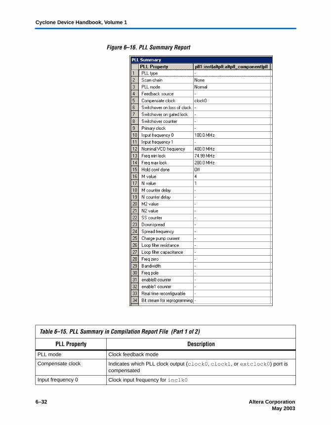
6–32 Altera CorporationPreliminary May 2003
Cyclone Device Handbook, Volume 1
Figure 6–16. PLL Summary Report
Table 6–15. PLL Summary in Compilation Report File (Part 1 of 2)
PLL Property Description
PLL mode Clock feedback mode
Compensate clock Indicates which PLL clock output (clock0, clock1, or extclock0) port is compensated
Input frequency 0 Clock input frequency for inclk0

Altera Corporation 6–33May 2003 Preliminary
Software Support
The PLL Usage report shows the breakdown information for each PLL clock output (see Figure 6–17). This report is categorized by PLL clock output ports, such that each row represents a different PLL clock output used in your design. Table 6–16 lists and explains the parameters shown in the PLL Usage report file in a row format. PLL parameters not listed in Table 6–16 do not apply to Cyclone PLLs.
Figure 6–17. PLL Usage Report
Timing Analysis
Table 6–16 shows the usage in the compilation report file.
Nominal VCO frequency Shows the VCO frequency; fVCO = fIN × M/N
Freq min lock Shows the minimum PLL input clock frequency for which the current combination of M/N still provides a valid VCO lock
Freq max lock Shows the maximum PLL input clock frequency for which the current combination of M/N still provides a valid VCO lock
M value M counter value
N value N counter value
Table 6–15. PLL Summary in Compilation Report File (Part 2 of 2)
PLL Property Description
Table 6–16. PLL Usage in Compilation Report File (Part 1 of 2)
PLL Parameter Description
Name Indicates the PLL instance name and clock output reported.
Output Clock Indicates the PLL clock output (clock0, clock1, or extclock0) for which the parameter information in this row applies. This is the clock port specified in the MegaWizard Plug-In Manager (c0, c1, e0).
Mult Overall multiplication ratio.
Div Overall division ratio.
Output Frequency Output frequency for this output clock.
Phase Shift Achieved phase shift in degrees and units of time (can differ from user-entered value).

6–34 Altera CorporationPreliminary May 2003
Cyclone Device Handbook, Volume 1
The register-to-register timing for each PLL clock output that drives the logic array is reported with slack. The timing analysis section of the report file provides slack information in a clock requirement line for each PLL clock output.
You can derive fMAX numbers from the slack reporting. The microparameters tCO, tSU, and the path delay are given for a List Path command on the Actual Maximum P2P timing in the Slack Report window. You can add and invert these to find the fMAX for that path. See the following equation:
fMAX = 1/(<register to register delay> - <clock skew delay> + <micro setup delay> + <micro clock to output delay>)
During timing analysis for Cyclone designs using PLLs, the project clock settings override the PLL input clock frequency and duty cycle settings. It is important to note the following:
A warning during compilation reports that the project clock settings override the PLL clock settings.
The project clock setting overrides the PLL clock settings for timing-driven compilation. When you compile a design with timing-driven compilation turned on, you are overconstraining the design so that the fitter can give you a better fMAX performance. For example, if the PLL is set to output a 150 MHz clock, you can set a project clock setting for 170 MHz so that the fitter tries to achieve a design performance of 170 MHz.
Duty Cycle Duty cycle for this clock output.
Counter Post-scale counter used for this clock output, which counter (G0, G1, E0) feeds the clock output.
Counter Value Value of post-scale counter.
High/Low High- and low-time counts that make up the counter value. The ratio of high- and low-counts is directly proportional to the duty cycle.
Initial Initial value for this post-scale counter (achieves the coarse granularity for phase shifting). Specifies the initial number of VCO cycles before starting the counter.
VCO Tap VCO tap ranges from 0 to 7 (achieves fine granularity for phase shift in units of 1/8 of the VCO period).
Table 6–16. PLL Usage in Compilation Report File (Part 2 of 2)
PLL Parameter Description

Altera Corporation 6–35May 2003 Preliminary
Software Support
The Compiler checks the lock frequency range of the PLL. If the frequency specified in the project clock settings is outside the lock frequency range, the PLL clock settings will not be overridden.
Overriding the PLL clock settings only changes the timing requirements; it does not change the overall multiplication/division and phase delay on each clock output of the PLL. The MegaWizard Plug-In Manager does not use the project clock settings to determine the altpll parameters.
Performing a timing analysis without recompiling your design does not change the programming files. You must recompile your design to update the programming files.
A Default Required fMAX setting does not override the PLL clock settings. Only individual clock settings will override the PLL clock settings.
This capability is useful when you have configured a Cyclone device and want to see if your timing requirements are met when you feed the PLL a different input clock than what is specified for the PLL parameters. Therefore, this feature allows you to overwrite the PLL input clock frequency settings for timing analysis, meaning you do not have to re-synthesize or re-fit your design. The following procedure allows you to override the PLL input frequency setting and re-generate timing analysis.
1. Choose Timing Settings (Project menu).
2. Click on the Clock Settings tab.
3. Under Specify circuit frequency as, select Settings for individual clock signals.
4. Click New.
5. In the New Clock Settings dialog box, type a <name> for the new clock settings in the Clock settings box.
6. If you want to specify timing requirements for an absolute clock, follow these steps:
a. Under Relationship to other clock settings, select Independent of other clock settings.
b. In the Required fMAX box, type the required frequency (fMAX) of the clock signal and select a time unit from the list.
6–36 Altera CorporationPreliminary May 2003
Cyclone Device Handbook, Volume 1
c. In the Duty Cycle list, specify the required duty cycle for the clock.
1 Cyclone PLLs accept input clocks with 40 to 60% duty cycle.
d. If you want to include external delays to and from device pins in the fMAX calculations, turn on Include external delays to and from device pins in fMAX calculations.
e. Click OK.
7. Click OK to close the Timing Settings window.
8. Open the Assignment Organizer dialog box (Tools menu).
9. Click on the By Node tab.
10. Under Mode, select Edit specific entity & node settings for.
11. If necessary, copy a specific PLL input clock pin name to the Name box using the Node Finder dialog box.
12. Under Assignment Categories, click the + icon next to Timing.
13. Click on Click here to add a new assignment.
14. Under Assignment, select Clock Settings in the Name list, and select the <name> of the clock settings you created in step 5.
15. Under Stored in assignments for, select This instance only, This instance in all occurrences of its parent entity, or Other.
16. Click Add.
17. Click OK or Apply.
18. Select Start Timing Analysis (Processing Menu).

Altera Corporation 6–37May 2003 Preliminary
Software Support
Simulation
The altpll megafunction supports behavioral and timing simulation in both the Quartus II software and supported third-party simulation tools. You can simulate all digital aspects of the PLL, but none of the analog aspects. Simulation supports all control signals and clock outputs. Table 6–17 explains the simulation support for altpll.
You can use the altpll behavioral model to simulate the Cyclone PLLs. The Cyclone behavioral model instantiation must follow the same guidelines and restrictions as the design entry. The altpll behavioral and timing models do not simulate jitter, lock time, or VCO drift.
The behavioral models for altpll reside in the \quartus\eda\sim_lib directory. ALTERA_MF.VHD contains the VHDL behavioral models and can be used for Cyclone designs that instantiate altpll. ALTERA_MF.v contains the Verilog HDL behavioral models. The behavioral model does not perform parameter error checking, and you must specify only valid values.
1 You must set the resolution of the simulator to units of pico seconds (ps) to simulate the model successfully. A larger resolution rounds off the calculations, providing incorrect results.
Table 6–17. altpll Simulation Support for Cyclone FPGAs
Feature Simulation Support
pllena The pllena signal is modeled. When this signal is driven low, the PLL loses lock and the PLL clock outputs are driven to logic low.
areset The areset signal is modeled. When this signal is driven high, the PLL loses lock and the PLL clock outputs are driven to logic low. Frequency over-shoot on the PLL clock outputs is not modeled.
pfdena The pfdena control signal is modeled. When this signal is driven low, the PLL’s locked output is undefined and the PLL clock outputs continue to toggle at their last set frequency. The finite frequency long-term drift of the VCO is not modeled.
locked The locked signal is modeled for a high-bandwidth condition only. The PLL locks or relocks within 2 to 10 cycles during simulation, and does not necessarily reflect the real lock time.
Frequency input change If the input frequency of the PLL is changed in simulation, the model checks that fIN × (M/N) is within the VCO frequency range and loses lock if outside the VCO operating range.
Jitter Jitter is not modeled in simulation.
6–38 Altera CorporationPreliminary May 2003
Cyclone Device Handbook, Volume 1
Global Clock Network
Cyclone FPGAs have eight global clock networks. The four dedicated clock input pins (CLK[3..0]), eight dual-purpose clock pins (DPCLK[7..0]), and PLL clock outputs can drive the global clock networks. In addition, internal logic for internally-generated global clocks and asynchronous clears, clock enables, or other control signals with large fanout can drive the global clock networks.
The eight global clock lines that comprise the global clock network drive throughout the entire device. You can use the global clock network as clock sources for all device resources, including IOEs, logic elements (LEs), and memory blocks. You can also use global clock resources for control signals, such as clock enables and synchronous or asynchronous clears fed from external pins.

Altera Corporation 6–39May 2003 Preliminary
Global Clock Network
Figure 6–18 shows the global clock network resources.
Figure 6–18. Global Clock Generation
Notes to Figure 6–18: (1) The EP1C3 device contains PLL1 only.(2) The EP1C3 device in the 100-pin TQFP package does not have dedicated clock pins CLK1 and CLK3.(3) The EP1C3 device in the 100-pin TQFP package has five DPCLK pins (DPCLK2, DPCLK3, DPCLK4, DPCLK6, and
DPCLK7). For more information, see "“Dual-Purpose Clock I/O Pins” on page 6–40.
8Global Clock
Network
PLL1 PLL2 (1)CLK0
(2) CLK1
CLK2
CLK3 (2)
(3) DPCLK1
(3)DPCLK0
DPCLK4
DPCLK5(3)
DPCLK2 DPCLK3
DPCLK7 DPCLK6
2 2
From CoreLogic
From CoreLogic
4 4
6–40 Altera CorporationPreliminary May 2003
Cyclone Device Handbook, Volume 1
Dedicated Clock Input Pins
Cyclone FPGAs have up to four dedicated clock input pins (CLK[3..0], two on the left and right side of the device. You can use the CLK[3..0] pins to drive the PLLs, or directly drive them onto the global clock network. Table 6–18 shows which clock pins drive which global clock network.
Dual-Purpose Clock I/O Pins
Cyclone FPGAs can have up to eight dual-purpose clock pins, DPCLK[7..0] (two on each side of the device). These dual-purpose pins can connect to the global clock network. You can use the DPCLK[7..0] pins for high fanout control signals, such as asynchronous clears, presets, clock enables, or protocol control signals (e.g., TRDY and IRDY for PCI, or DQS signals for external memory interfaces). These pins are also available as general-purpose I/O pins, meaning they can be inputs, outputs, or bidirectional pins. Table 6–19 shows which dual-purpose clock pins drive which global clock network in Cyclone FPGAs.
Table 6–18. Dedicated Clock Input Pin Connections to Global Clock Network
Clock Input Pin GCLK0 GCLK1 GCLK2 GCLK3 GCLK4 GCLK5 GCLK6 GCLK7
CLK0 v v
CLK1 (1) v v
CLK2 v v
CLK3 (1) v v
Note to Table 6–18: (1) The EP1C3 device in the 100-pin TQFP package does not have dedicated clock pins CLK1 and CLK3.
Table 6–19. Dual-Purpose Clock I/O Connections to the Global Clock Network (Part 1 of 2)
Dual-Purpose Clock Pin
GCLK0 GCLK1 GCLK2 GCLK3 GCLK4 GCLK5 GCLK6 GCLK7
DPCLK0(1) v
DPCLK1(1) v
DPCLK2 v
DPCLK3 v
DPCLK4 v

Altera Corporation 6–41May 2003 Preliminary
Global Clock Network
Combined Sources
Table 6–20 shows which combined sources drive which global clock network.
DPCLK5(1) v
DPCLK6 v
DPCLK7 v
Note to Table 6–19:(1) The EP1C3 device in the 100-pin TQFP package does not have the DPCLK0, DPCLK1, or DPCLK5 pins
Table 6–19. Dual-Purpose Clock I/O Connections to the Global Clock Network (Part 2 of 2)
Dual-Purpose Clock Pin
GCLK0 GCLK1 GCLK2 GCLK3 GCLK4 GCLK5 GCLK6 GCLK7
Table 6–20. Global Clock Network Sources (Part 1 of 2)
Source GCLK0 GCLK1 GCLK2 GCLK3 GCLK4 GCLK5 GCLK6 GCLK7
PLL Counter Outputs
PLL1 G0 v v
PLL1 G1 v v
PLL2 G0 (1) v v
PLL2 G1 (1) v v
Dedicated Clock
Input Pins
CLK0 v v
CLK1 (2) v v
CLK2 v v
CLK3 (2) v v

6–42 Altera CorporationPreliminary May 2003
Cyclone Device Handbook, Volume 1
In the Cyclone FPGA, there are eight distinct dedicated global clock networks. Multiplexers are used with these clocks to form six-bit buses to drive LAB row clocks, column IOE clocks, or row IOE clocks (see Figure 6–19). Another multiplexer is used at the LAB level to select two of the six row clocks to feed the LE registers within the LAB.
Figure 6–19. Global Clock Network Multiplexers
IOE clocks have horizontal (row) and vertical (column) block regions that are clocked by six I/O clock signals chosen from the eight global clock resources. Figure 6–20 shows the I/O clock regions.
Dual-Purpose
Clock Pins
DPCLK0 v
DPCLK1 (3) v
DPCLK2 v
DPCLK3 v
DPCLK4 v
DPCLK5 v
DPCLK6 v
DPCLK7 v
Notes to Table 6–20:(1) The EP1C3 device only has PLL1.(2) The EP1C3 device in the 100-pin TQFP package does not have dedicated clock pins CLK1 and CLK3.(3) The EP1C3 device does not have DPCLK1.
Table 6–20. Global Clock Network Sources (Part 2 of 2)
Source GCLK0 GCLK1 GCLK2 GCLK3 GCLK4 GCLK5 GCLK6 GCLK7
Clock [7..0]
Column I/O RegionIO_CLK[5..0]
Lab Row Clock [5..0]
Row I/O RegionIO_CLK[5..0]
Dedicated Clock Inputs [3..0]
PLL Outputs [3..0]
Dual-Purpose Clock I/Os [7..0]
Global ClockNetwork
Core Logic [7..0]
4
8
4
8
8 6
6
6
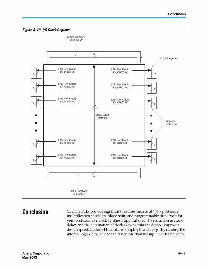
Altera Corporation 6–43May 2003 Preliminary
Conclusion
Figure 6–20. I/O Clock Regions
Conclusion Cyclone PLLs provide significant features such as M/(N × post-scale) multiplication/division, phase shift, and programmable duty cycle for your cost-sensitive clock synthesis applications. The reduction in clock delay, and the elimination of clock skew within the device, improves design speed. Cyclone PLL features simplify board design by running the internal logic of the device at a faster rate than the input clock frequency.
Vertical I/O RegionIO_CLK[5..0]
6
6 6
6
I/O Clock Regions
8
Global ClockNetwork
LAB Row ClocksIO_CLK[5..0]
Vertical I/O RegionIO_CLK[5..0]
6
LAB Row ClocksIO_CLK[5..0]
6
LAB Row ClocksIO_CLK[5..0]
6
LAB Row ClocksIO_CLK[5..0]
6
LAB Row ClocksIO_CLK[5..0]
LAB Row ClocksIO_CLK[5..0]
6
LAB Row ClocksIO_CLK[5..0]
6
LAB Row ClocksIO_CLK[5..0]
6
LAB Row ClocksIO_CLK[5..0]
6
LAB Row ClocksIO_CLK[5..0]
HorizontalI/O Regions

6–44 Altera CorporationPreliminary May 2003
Cyclone Device Handbook, Volume 1

Altera Corporation Part III–1Preliminary
Section III. Memory
This section provides information on the M4K embedded memory blocks internal to Cyclone devices.
It contains the following:
Chapter 7. On-Chip Memory Implementations Using Cyclone Memory Blocks
Revision History The table below shows the revision history for Chapter 7.
Chapter(s) Date / Version Changes Made
7 May 2003v1.0
Updated Table 7–2 with EP1C4.

Part III–2 Altera CorporationPreliminary
Memory Cyclone Device Handbook, Volume 1
Altera Corporation 7–1May 2003 Preliminary
7. On-Chip MemoryImplementations Using
Cyclone Memory Blocks
Introduction CycloneTM devices feature embedded memory blocks that can be easily configured to support a wide range of system requirements. These M4K memory blocks present a very flexible and fast memory solution that you can use to provide excellent memory bandwidth and density for a host of cost-sensitive applications.
You can use M4K memory blocks in various memory modes, including single-port, simple dual-port, true dual-port (also known as bidirectional dual-port), shift-register, ROM, and first-in first-out (FIFO) mode. M4K memory blocks also include advanced features such as support for byte-enable operation, parity-bit-based error correction, and mixed-port widths. This application note describes these modes and other characteristics of the M4K memory blocks.
M4K Memory Features
Table 7–1 summarizes the features supported by the M4K memory block.
Table 7–1. Summary of M4K Memory Features (Part 1 of 2)
Performance 200 MHz
Total RAM bits (including parity bits) 4,608
Configurations 4K × 12K × 21K × 4512 × 8512 × 9
256 × 16256 × 18128 × 32
128 × 36 (1)
Parity bits v
Byte enable v
Single-port memory v
Simple dual-port memory v
True dual-port memory v
Embedded shift register v
ROM v
C51007-1.0

7–2 Altera CorporationPreliminary May 2003
Cyclone Device Handbook, Volume 1
Table 7–2 shows the memory capacity for M4K memory blocks in each Cyclone device.
Parity Bit Support
M4K memory blocks support an optional parity bit for each data byte. Of the 4,608 bits of storage space available in an M4K block, 512 are available for use as parity-bit storage. The parity bit, along with logic implemented in logic elements (LEs), can facilitate parity-checking methods of error detection to ensure data integrity. You can also use parity-size data words to store user-specified control bits or as extra data bits to provide support for 9-bit, 18-bit, or 36-bit wide memories.
FIFO buffer v
Simple dual-port mixed width support v
True dual-port mixed width support v
Memory initialization (.mif) v
Mixed-clock mode v
Power-up condition Outputs cleared
Register clears Input and output registers (2)
Same-port read-during-write New data available at positive clock edge
Mixed-port read-during-write Outputs set to unknown or old data
Notes to Table 7–1:(1) The Altera® Quartus® II software will automatically cascade or concatenate
multiple M4K memory blocks to provide deeper or wider memory functions.(2) Asserting the clear port of the rden and byte-enable registers drives the output
of these registers high.
Table 7–2. M4K Memory Distribution in Cyclone Devices
Device Columns Blocks Total RAM Bits
EP1C3 1 13 59,904
EP1C4 1 17 78,336
EP1C6 1 20 92,160
EP1C12 2 52 239,616
EP1C20 2 64 294,912
Table 7–1. Summary of M4K Memory Features (Part 2 of 2)
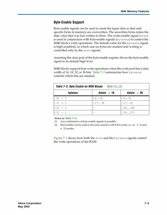
Altera Corporation 7–3May 2003 Preliminary
M4K Memory Features
Byte-Enable Support
Byte-enable signals can be used to mask the input data so that only specific bytes in memory are overwritten. The unwritten bytes retain the data value that was last written to them. The write-enable signal (wren) is used in conjunction with byte-enable signals (byteena) to control the M4K block's write operations. The default value for the byteena signal is high (enabled), in which case no bytes are masked and writing is controlled only by the wren signals.
Asserting the clear port of the byte-enable register drives the byte-enable signal to its default high level.
M4K blocks support byte write operations when the write port has a data width of 16, 18, 32, or 36 bits. Table 7–3 summarizes how byteena controls which bits are masked.
Figure 7–1 shows how both the wren and the byteena signals control the write operations of the RAM.
Table 7–3. Byte Enable for M4K Blocks Note (1), (2)
byteena datain × 18 datain × 36
[0] = 1 [8..0] [8..0]
[1] = 1 [17..9] [17..9]
[2] = 1 - [26..18]
[3] = 1 - [35..27]
Notes to Table 7–3:(1) Any combination of byte-enable signals is possible.(2) Byte enables can be used in the same manner with 8-bit words, i.e., in × 16 and
× 32 modes.

7–4 Altera CorporationPreliminary May 2003
Cyclone Device Handbook, Volume 1
Figure 7–1. Byte-Enable Operation Functional Waveform
Power-up Conditions & Memory Initialization
Upon power-up, M4K memory is in an idle state. The outputs always power-up to zero, regardless of whether the output registers are used or bypassed. Even if a memory initialization file is used to pre-load the contents of the RAM block, the outputs will still power-up cleared. For example, if address 0 is pre-initialized to FF, the M4K blocks power-up with the output at 00.
Using M4K Memory
M4K memory blocks include input registers that synchronize write operations and output registers to pipeline designs and improve system performance. All M4K memory blocks are fully synchronous, meaning that all inputs are registered, but outputs can be either registered or combinatorial. M4K memory can emulate asynchronous memory.
f For more information, see Application Note 210: Converting Memory from Asynchronous to Synchronous for Stratix Designs.
inclock
wren
address
data_in
asynch_data_out
an
XXXX
a0 a1 a2 a0 a1 a2
doutn ABXX XXCD ABCD ABFF FFCD
ABCD
byteena XX 10 01 11
XXXX
XX
ABCD
ABCDFFFF
FFFF
FFFF
ABFF
FFCD
contents at a0
contents at a1
contents at a2
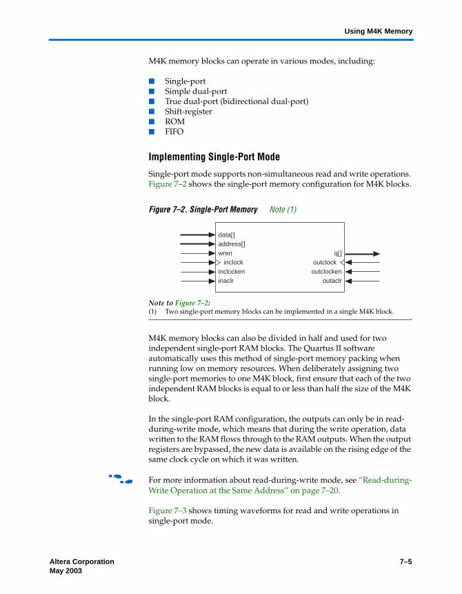
Altera Corporation 7–5May 2003 Preliminary
Using M4K Memory
M4K memory blocks can operate in various modes, including:
Single-port Simple dual-port True dual-port (bidirectional dual-port) Shift-register ROM FIFO
Implementing Single-Port Mode
Single-port mode supports non-simultaneous read and write operations. Figure 7–2 shows the single-port memory configuration for M4K blocks.
Figure 7–2. Single-Port Memory Note (1)
Note to Figure 7–2:(1) Two single-port memory blocks can be implemented in a single M4K block.
M4K memory blocks can also be divided in half and used for two independent single-port RAM blocks. The Quartus II software automatically uses this method of single-port memory packing when running low on memory resources. When deliberately assigning two single-port memories to one M4K block, first ensure that each of the two independent RAM blocks is equal to or less than half the size of the M4K block.
In the single-port RAM configuration, the outputs can only be in read-during-write mode, which means that during the write operation, data written to the RAM flows through to the RAM outputs. When the output registers are bypassed, the new data is available on the rising edge of the same clock cycle on which it was written.
f For more information about read-during-write mode, see “Read-during-Write Operation at the Same Address” on page 7–20.
Figure 7–3 shows timing waveforms for read and write operations in single-port mode.
data[ ]address[ ]wren inclockinclockeninaclr
q[ ]outclock outclocken
outaclr

7–6 Altera CorporationPreliminary May 2003
Cyclone Device Handbook, Volume 1
Figure 7–3. Single-Port Timing Waveforms
Implementing Simple Dual-Port Mode
Simple dual-port memory supports simultaneous read and write operations. Figure 7–4 shows the simple dual-port memory configuration for M4K blocks.
Figure 7–4. Simple Dual-Port Memory Note (1)
Note to Figure 7–4:(1) Simple dual-port RAM supports read/write clock mode in addition to the
input/output clock mode shown.
M4K memory supports mixed-width configurations, allowing different read and write port widths. This capability is useful for many applications, including implementing serializer-deserializers (SERDES)
in clock
wren
address
data_in
synch_data_out
an-1
din-1 din din4 din5
a6
din6
an a0 a1 a2 a3 a4 a5
asynch_data_out
din-2 din-1 din dout0 dout1 dout2 dout3 din4
din-1 din dout0 dout1 dout2 dout3 din4 din5
data[ ]wraddress[ ]wren inclockinclockeninaclr
rdaddress[ ]rden
q[ ]outclock outclocken
outaclr

Altera Corporation 7–7May 2003 Preliminary
Using M4K Memory
as well as interfacing with buses of differing widths. Table 7–4 shows the mixed-width configurations supported by the M4K blocks in Cyclone devices..
In simple dual-port mode, M4K blocks have one write-enable and one read-enable signal. On the M4K block, asserting the clear port of the rden register drives rden high, which allows the read operation to occur. When the read-enable signal is deactivated, the current data is retained at the output ports. If the read-enable signal is activated during a write operation with the same address location selected, the simple dual-port RAM output is either unknown or can be set to output the old data stored at the memory address.
f For more information, see “Read-during-Write Operation at the Same Address” on page 7–20.
Figure 7–5 shows timing waveforms for read and write operations in simple dual-port mode.
Table 7–4. M4K Block Mixed-Width Configurations (Simple Dual-Port Mode)
Read Port
Write Port
4K × 1 2K × 2 1K × 4 512 × 8 256 × 16 128 × 32 512 × 9 256 × 18 128 × 36
4K × 1 v v v v v v
2K × 2 v v v v v v
1K × 4 v v v v v v
512 × 8 v v v v v v
256 × 16 v v v v v v
128 × 32 v v v v v v
512 × 9 v v v
256 × 18 v v v
128 × 36 v v v

7–8 Altera CorporationPreliminary May 2003
Cyclone Device Handbook, Volume 1
Figure 7–5. Simple Dual-Port Timing Waveforms
Implementing True Dual-Port Mode
M4K blocks offer a true dual-port mode to support any combination of two-port operations: two read operations, two write operations, or one read operation and one write operation at two different clock frequencies. True dual-port memory can be used to increase memory bandwidth in numerous applications. An example system that benefits from the use of true dual-port memory is a system containing an Altera Nios® embedded processor and a direct memory access (DMA) controller. Such a system will experience bottlenecks if the processor and the DMA controller need simultaneous access to single-port memory. The ability of both the processor and the DMA controller to access the M4K memory simultaneously, avoiding the need for arbitration, can dramatically improve bandwidth in this type of system.
Figure 7–6 shows the true dual-port memory configuration for M4K blocks.
wrclock
wren
wraddress
data_in
synch_data_out
an-1 an a0 a1 a2 a3 a4 a5
din-1 din din4 din5
rdclock
a6
din6
asynch_data_out
rden
rdaddress bn b0 b1 b2 b3
doutn-2 doutn-1 doutn
doutn-1 doutn dout0

Altera Corporation 7–9May 2003 Preliminary
Using M4K Memory
Figure 7–6. True Dual-Port Memory Note (1)
Note to Figure 7–6:(1) True dual-port memory supports input/output clock mode in addition to the
independent clock mode shown.
The widest bit configuration of a single M4K block in true dual-port mode is 256 × 16-bit (or 256 × 18-bit with parity). The 128 × 32-bit (128 × 36-bit with parity) configuration of the M4K block is unavailable because the number of output drivers is equivalent to the maximum bit width of the M4K block. Because true dual-port RAM has outputs on two ports, the maximum width of the true dual-port RAM equals half of the total number of output drivers. However, multiple M4K blocks can be concatenated to support wider memory configurations. Table 7–5 lists the possible M4K RAM block configurations.
Table 7–5. M4K Block Mixed-Port Width Configurations (True Dual-Port Mode)
Port APort B
4K × 1 2K × 2 1K × 4 512 × 8 256 × 16 512 × 9 256 × 18
4K × 1 v v v v v
2K × 2 v v v v v
1K × 4 v v v v v
512 × 8 v v v v v
256 × 16 v v v v v
512 × 9 v v
256 × 18 v v
dataA[ ]addressA[ ]wrenA
clockA
clockenA
qA[ ]aclrA
dataB[ ]addressB[ ]
wrenB
clockB clockenB
qB[ ]aclrB
A B

7–10 Altera CorporationPreliminary May 2003
Cyclone Device Handbook, Volume 1
In true dual-port mode, the RAM outputs can only be configured for read-during-write mode. This means that during write operation, data being written to the A or B port of the RAM flows through to the A or B outputs, respectively. When the output registers are bypassed, the new data is available on the rising edge of the same clock cycle it was written on.
f For sample waveforms and other information on mixed-port read-during-write mode, see “Read-during-Write Operation at the Same Address” on page 7–20.
Potential write conflicts must be resolved external to the RAM because simultaneously writing to the same address location at both ports results in unknown data storage at that location. For a valid write operation to the same address of the RAM block, the rising edge of the write clock for port A must occur following the minimum write cycle time interval after the rising edge of the write clock for port B. Since data is written into the M4K blocks at the falling edge of the write clock, the rising edge of the write clock for port A should occur following half of the minimum write cycle time interval after the falling edge of the write clock for port B. If this timing is not met, the data stored in that particular address will be invalid.
f See Section I, Cyclone FPGA Family Data Sheet for more information about the minimum synchronous write cycle time.
Figure 7–7 shows true dual-port timing waveforms for a write operation at port A and a read operation at port B.

Altera Corporation 7–11May 2003 Preliminary
Using M4K Memory
Figure 7–7. True Dual-Port Timing Waveforms
Implementing Shift-Register Mode
Embedded memory configurations can implement shift-register blocks for digital signal processing (DSP) applications, such as finite impulse response (FIR) filters, pseudo-random number generators, multi-channel filtering, and auto-correlation and cross-correlation functions. These and other DSP applications require local data storage, traditionally implemented with standard flip-flops that can quickly consume many logic cells for large shift registers. A more efficient alternative is to use embedded memory as a shift-register block, which saves logic cell and routing resources and provides a more efficient implementation.
The size of a (w × m × n) shift register is determined by the input data width (w), the length of the taps (m), and the number of taps (n). The size of a (w × m × n) shift register must be less than or equal to the 4,608 bits. In addition, the size of (w × n) must be less than or equal to 36 bits. If a larger shift register is required, memory blocks can be cascaded together.
Data is written into each address location at the falling edge of the clock and read from the address at the rising edge of the clock. The shift-register mode logic automatically controls the positive and negative edge clocking to shift the data in one clock cycle. Figure 7–8 shows the M4K memory block in shift-register mode.
A_clk
A_wren
A_address
A_data_in
B_synch_data_out
an-1 an a0 a1 a2 a3 a4 a5
din-1 din din4 din5
B_clk
a6
din6
B_asynch_data_out
B_wren
B_address bn b0 b1 b2 b3
doutn-2 doutn-1 doutn
doutn-1 doutn dout0
A_synch_data_out
A_asynch_data_out
dout0
dout1
dout1
dout2
din-2 din-1 din dout0 dout1 dout2 dout3 din4
din-1 din dout0 dout1 dout2 dout3 din4 din5

7–12 Altera CorporationPreliminary May 2003
Cyclone Device Handbook, Volume 1
Figure 7–8. M4K Shift-Register Memory Configuration
Implementing ROM Mode
M4K blocks can also be configured as ROM. ROM can be initialized in an M4K block by using a memory initialization file (.mif). Because all M4K memory configurations must have synchronous inputs, the address lines of the ROM are registered. ROM outputs can be registered or combinatorial. The read operation of the ROM is identical to the read operation of the single-port RAM configuration.
Implementing FIFO Buffers
FIFO buffer outputs are always combinatorial. Simultaneous read and write operations from an empty FIFO buffer are not supported.
m-Bit Shift Registerw w
m-Bit Shift Register
m-Bit Shift Register
m-Bit Shift Register
w w
w w
w w
w × m × n Shift Register
n Numberof Taps
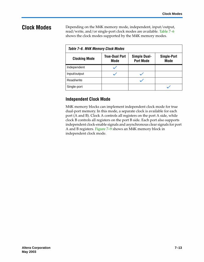
Altera Corporation 7–13May 2003 Preliminary
Clock Modes
Clock Modes Depending on the M4K memory mode, independent, input/output, read/write, and/or single-port clock modes are available. Table 7–6 shows the clock modes supported by the M4K memory modes.
Independent Clock Mode
M4K memory blocks can implement independent clock mode for true dual-port memory. In this mode, a separate clock is available for each port (A and B). Clock A controls all registers on the port A side, while clock B controls all registers on the port B side. Each port also supports independent clock-enable signals and asynchronous clear signals for port A and B registers. Figure 7–9 shows an M4K memory block in independent clock mode.
Table 7–6. M4K Memory Clock Modes
Clocking Mode True-Dual Port Mode
Simple Dual-Port Mode
Single-Port Mode
Independent v
Input/output v v
Read/write v
Single-port v

7–14 Altera CorporationPreliminary May 2003
Cyclone Device Handbook, Volume 1
Figure 7–9. Independent Clock Mode
8D E
NA
Q
D EN
A
Q
D EN
A
Q
data
A[ ]
addr
ess A
[ ]
Mem
ory
Blo
ck25
6 ´
16 (
2)51
2 ´
81,
024
´ 4
2,04
8 ´
24,
096
´ 1
Dat
a In
Add
ress
A
Writ
e/R
ead
Ena
ble
Dat
a O
ut
Dat
a In
Add
ress
B
Writ
e/R
ead
Ena
ble
Dat
a O
ut
clke
n A
cloc
k A
D EN
A
Q
wre
n A
8 LA
B R
ow C
lock
s
q A[ ]
8da
taB[ ]
addr
ess B
[ ]
clke
n B
cloc
k B
wre
n B
q B[ ]
EN
A
AB
EN
ADQ
D EN
A
Qby
teen
a A[ ]
Byt
e E
nabl
e A
Byt
e E
nabl
e B
byte
ena B
[ ]
EN
ADQ
EN
ADQ
EN
ADQ
DQ
Writ
eP
ulse
Gen
erat
or
Writ
eP
ulse
Gen
erat
or

Altera Corporation 7–15May 2003 Preliminary
Clock Modes
Input/Output Clock Mode
M4K memory blocks can implement input/output clock mode for true and simple dual-port memory. On each of the two ports, A and B, one clock controls all registers for inputs (data input, wren, and address) into the memory block. The other clock controls the block's data output registers. Each memory block port also supports independent clock enables and asynchronous clear signals for input and output registers. Figures 7–10 and 7–11 show the memory block in input/output clock mode for true and simple dual-port modes, respectively.

7–16 Altera CorporationPreliminary May 2003
Cyclone Device Handbook, Volume 1
Figure 7–10. Input/Output Clock Mode in True Dual-Port Mode
8
D EN
A
Q
D EN
A
Q
D EN
A
Q
data
A[ ]
addr
ess A
[ ]
Mem
ory
Blo
ck25
6 ×
16 (2
)51
2 ×
81,
024
× 4
2,04
8 ×
24,
096
× 1
Dat
a In
Add
ress
A
Writ
e/R
ead
Ena
ble
Dat
a O
ut
Dat
a In
Add
ress
B
Writ
e/R
ead
Ena
ble
Dat
a O
ut
clke
n A
cloc
k A
D EN
A
Q
wre
n A
8 LA
B R
ow C
lock
s
q A[ ]
8
data
B[ ]
addr
ess B
[ ]
clke
n B
cloc
k B
wre
n B
q B[ ]
EN
A
AB
EN
ADQ
EN
ADQ
EN
ADQ
DQ
D EN
A
Qby
teen
a A[ ]
Byt
e E
nabl
e A
Byt
e E
nabl
e B
byte
ena B
[ ]
EN
ADQ
Writ
eP
ulse
Gen
erat
or
Writ
eP
ulse
Gen
erat
or

Altera Corporation 7–17May 2003 Preliminary
Clock Modes
Figure 7–11. Input/Output Clock Mode in Simple Dual-Port Mode Note (1)
Note to Figure 7–11:(1) For more information on the MultiTrackTM interconnect, see Section I, Cyclone FPGA Family Data Sheet.
Read/Write Clock Mode
M4K memory blocks can implement read/write clock mode for simple dual-port memory. This mode can use up to two clocks. The write clock controls the block's data inputs, wraddress, and wren. The read clock controls the data output, rdaddress, and rden. The memory blocks support independent clock enables for each clock and asynchronous clear signals for the read- and write-side registers. Figure 7–12 shows a memory block in read/write clock mode.
8
DENA
Q
D
ENA
Q
D
ENA
Q
D
ENA
Q
DENA
Q
data[ ]
DENA
Qwraddress[ ]
address[ ]
Memory Block256 ´ 16
512 ´ 81,024 ´ 42,048 ´ 24,096 ´ 1
Data In
Read Address
Write Address
Write Enable
Read Enable
Data Out
outclken
inclken
wrclock
rdclock
wren
rden
8 LAB Row Clocks
To MultiTrackInterconnect
DENA
Qbyteena[ ] Byte Enable
WritePulse
Generator

7–18 Altera CorporationPreliminary May 2003
Cyclone Device Handbook, Volume 1
Figure 7–12. Read/Write Clock Mode in Simple Dual-Port Mode Note (1)
Note to Figure 7–12:(1) For more information on the MultiTrack interconnect, see Section I, Cyclone FPGA Family Data Sheet.
Single-Port Mode
The M4K memory blocks can implement single-port clock mode when simultaneous read and write operations are not required (see Figure 7–13). A single block in a memory block can support up to two single-port mode RAM blocks in M4K blocks.
8
DENA
Q
D
ENA
Q
D
ENA
Q
D
ENA
Q
DENA
Q
data[ ]
DENA
Qwraddress[ ]
address[ ]
Memory Block256 × 16512 × 8
1,024 × 42,048 × 24,096 × 1
Data In
Read Address
Write Address
Write Enable
Read Enable
Data Out
outclken
inclken
wrclock
rdclock
wren
rden
8 LAB RowClocks
To MultiTrackInterconnect
DENA
Qbyteena[ ] Byte Enable
WritePulse
Generator

Altera Corporation 7–19May 2003 Preliminary
Synchronous & Pseudo-Asynchronous Modes
Figure 7–13. Single-Port Mode Note (1)
Note to Figure 13:(1) For more information on the MultiTrack interconnect, see Section I, Cyclone FPGA Family Data Sheet.
Synchronous & Pseudo-Asynchronous Modes
The M4K memory architecture implements synchronous, pipelined RAM by registering both the input and output signals to the RAM block. All M4K memory inputs are registered, providing synchronous write cycles. In synchronous operation, an M4K block generates its own self-timed strobe write enable (wren) signal derived from the global or regional clock. In contrast, a circuit using asynchronous RAM must generate the RAM wren signal while ensuring its data and address signals meet setup and hold time specifications relative to the wren signal. The output registers can be bypassed.
In an asynchronous memory, neither the input nor the output is registered. While Cyclone devices do not support asynchronous memory, they do support a pseudo-asynchronous read operation where the output data is available during the same clock cycle as when the read address is driven into it. Pseudo-asynchronous reading is possible in the simple and
8
DENA
Q
D
ENA
Q
D
ENA
Q
DENA
Q
data[ ]
address[ ]
RAM/ROM256 × 16
512 × 81,024 × 42,048 × 24,096 × 1
Data In
Address
Write Enable
Data Out
outclken
inclken
inclock
outclock
WritePulse
Generator
wren
8 LAB RowClocks
To MultiTrackInterconnect

7–20 Altera CorporationPreliminary May 2003
Cyclone Device Handbook, Volume 1
true dual-port modes of the M4K blocks by clocking the read enable and read address registers on the negative clock edge and bypassing the output registers.
f For more information, see AN 210: Converting Memory from Asynchronous to Synchronous for Stratix Designs.
Read-during-Write Operation at the Same Address
The following two sections describe the functionality of the various M4K memory configurations when reading from an address during a write operation at that same address. There are two types of read-during-write operations: same-port and mixed-port. Figure 7–14 illustrates the difference in data flow between same-port and mixed-port read-during-write.
Figure 7–14. Read-during-Write Data Flow
Same-Port Read-during-Write Mode
For read-during-write operation of a single-port RAM or the same port of a true dual-port RAM, the new data is available on the rising edge of the same clock cycle it was written on. See Figure 7–15 for a sample functional waveform.
When using byte-enable signals in true dual-port RAM mode, the outputs for the masked bytes on the same port are unknown. (See Figure 7–1.) The non-masked bytes are read out as shown in Figure 7–15.
Port Adata in
Port Bdata in
Port Bdata out
Port Adata out
Same-portdata flow
Mixed-portdata flow

Altera Corporation 7–21May 2003 Preliminary
Read-during-Write Operation at the Same Address
Figure 7–15. Same-Port Read-during-Write Functionality Note (1)
Note to Figure 7–15:(1) Outputs are not registered.
Mixed-Port Read-during-Write Mode
This mode is used when a RAM in simple or true dual-port mode has one port reading and the other port writing to the same address location with the same clock. You can configure the M4K memory block to operate in this mode and modify the parameter shown below using the MegaWizard® Plug-In Manager included with the Quartus II software.
The READ_DURING_WRITE_MODE_MIXED_PORTS parameter for M4K memory blocks determines whether or not to output the old data at the address. Setting this parameter to OLD_DATA outputs the old data at that address. Setting this parameter to DONT_CARE outputs an unknown value. During the instantiation of an ALTSYNCRAM or LPM_RAM_DP+ storage megafunction using the Quartus II software, the MegaWizard plug-in manager asks “How should the q output behave when reading a memory location that is being written from the other port?” Clicking “I don’t care” assigns the DONT_CARE value to the parameter, and clicking “Old memory contents appear” assigns the OLD_DATA value to the parameter.
1 Altera recommends using the MegaWizard Plug-In Manager to create these memory megafunctions rather than directly creating instances. Once a storage megafunction is created using the MegaWizard Plug-In Manager, use the MegaWizard Plug-In Manager to make any necessary changes.
See Figures 7–16 and 7–17 for sample functional waveforms showing mixed-port read-during-write mode operation. These figures assume that the outputs are not registered.
inclock
data_in
wren
data_out A
BA
Old

7–22 Altera CorporationPreliminary May 2003
Cyclone Device Handbook, Volume 1
Figure 7–16. Mixed-Port Read-during-Write: OLD_DATA
Figure 7–17. Mixed-Port Read-during-Write: DONT_CARE
When two different clocks are used in dual-port RAM, the read-during-write behavior depends on the relationship of the clocks. The writing of the new contents starts at the falling edge of the write clock. Therefore, if the read clock's rising edge occurs before the falling edge of the write clock, the old data is read out. If the read clock's rising edge occurs between the falling edge of the write clock and half the minimum write cycle time interval, the output is unknown data.
f For the minimum synchronous-write-cycle time see Section I, Cyclone FPGA Family Data Sheet.
inclock
Port Adata_in
Port Awren
Port Bdata_out
A B
AOld
Port Bwren
B
Address QaddressA and
addressB
inclock
Port Adata_in
Port Awren
Port Bdata_out
A B
BUnknown
Port Bwren
Address QaddressA and
addressB

Altera Corporation 7–23May 2003 Preliminary
Conclusion
Conclusion M4K memory blocks are a flexible memory solution available in Cyclone devices that provide advanced features such as byte-enable capability, parity bit storage capability, and shift-register mode, as well as mixed-port width support and true dual-port mode. This flexibility makes these embedded memory blocks well suited for a wide range of applications including ATM cell packet processing, header/cell storage, channelized functions, and program memory for processors.

7–24 Altera CorporationPreliminary May 2003
Cyclone Device Handbook, Volume 1

Altera Corporation Section IV–1Preliminary
Section IV. I/O Standards
This section provides information on the Cyclone FPGA I/O capabilities. It also includes information on selecting I/O standards for Cyclone devices in the Quartus II software.
This section contains the following chapters:
Chapter 8. Using Selectable I/O Standards in Cyclone Devices
Chapter 9. Implementing LVDS in Cyclone Devices
Revision History The table below shows the revision history for Chapter 8 and 9.
Chapter(s) Date / Version Changes Made
8 May 2003v1.0
Added Figure 8–5 and section titled “Differential SSTL-2 - EIA/JEDEC Standard JESD8-9A”. Added last row to Table 8–1 for Differential SSTL - 2.
9 May 2003v1.0
Revised Table 9–1 with EP1C4.

Section IV–2 Altera CorporationPreliminary
I/O Standards Cyclone Device Handbook, Volume 1

Altera Corporation 8–1May 2003 Preliminary
8. Using Selectable I/OStandards in Cyclone Devices
Introduction The proliferation of I/O standards and the need for improved I/O performance have made it critical that low-cost devices have flexible I/O capabilities. Selectable I/O capabilities such as SSTL-2, SSTL-3, and LVDS compatibility allow Cyclone™ devices to connect to other devices on the same printed circuit board (PCB) that may require different operating and I/O voltages. With these aspects of implementation easily manipulated using the Altera® Quartus® II software, the Cyclone device family enables system designers to use low-cost FPGAs while keeping pace with increasing design complexity.
This application note is a guide to understanding the input/output capabilities of the Cyclone devices, including:
Supported I/O Standards Cyclone I/O Banks Programmable Current Drive Strength Hot Socketing I/O Termination Pad Placement & DC Guidelines Quartus II Software Support
“Quartus II Software Support” on page 8–17 describes how to use the Quartus II software to specify device and pin options and assign pins to implement the above features of Cyclone devices.
C51008-1.0

8–2 Altera CorporationPreliminary May 2003
Cyclone Device Handbook, Volume 1
Supported I/O Standards
Cyclone devices support the I/O standards shown in Table 8–1.
f See Section I, Cyclone FPGA Family Data Sheet for more details on the I/O Standards discussed in this section.
3.3-V LVTTL (EIA/JEDEC Standard JESD8-B)
The 3.3-V LVTTL I/O standard is a general-purpose, single-ended standard used for 3.3-V applications. The LVTTL standard defines the DC interface parameters for digital circuits operating from a 3.0-V/3.3-V power supply and driving or being driven by LVTTL-compatible devices.
Table 8–1. I/O Standards Supported by Cyclone Devices Notes (1), (2)
I/O Standard Type Input Voltage Level (V)
Output Voltage
Level (V)
Input VREF (V)
Output VCCIO (V)
Termination VTT (V)
3.3-V LVTTL/LVCMOS
Single-ended 3.3/2.5 3.3 N/A 3.3 N/A
2.5-V LVTTL/LVCMOS
Single-ended 3.3/2.5 2.5 N/A 2.5 N/A
1.8-V LVTTL/LVCMOS
Single-ended 3.3/2.5/1.8 1.8 N/A 1.8 N/A
1.5-V LVCMOS Single-ended 3.3/2.5/1.8/1.5 1.5 N/A 1.5 N/A
PCI Single-ended 3.3 3.3 N/A 3.3 N/A
SSTL-3 Class I and II
Voltage-referenced -0.3 to 3.9 3.3 1.5 3.3 1.5
SSTL-2 Class I and II
Voltage-referenced -0.3 to 3.0 2.5 1.25 2.5 1.25
LVDS Compatibility
Differential 0 to 2.4 VOD = 0.25 to 0.55
N/A 2.5 N/A
Differential SSTL - 2
Differential N/A (3) 2.5 1.25 2.5 1.25
Notes to Table 8–1:(1) The EP1C3 device in the 100-pin thin quad flat pack (TQFP) package does not have support for a PLL LVDS input
or an external clock output.(2) Cyclone devices have dual-purpose differential inputs. Outputs are balanced SSTL outputs requiring an external
resistor divider.(3) This I/O standard is only available on output clock pins (PLL_OUT pins).

Altera Corporation 8–3May 2003 Preliminary
Supported I/O Standards
The LVTTL input standard specifies a wider input voltage range of - 0.3 V ≤ VI ≤ 3.9 V. Altera recommends an input voltage range of - 0.5 V ≤ VI ≤ 4.1 V. The LVTTL standard does not require input reference voltages or board terminations. Cyclone devices support both input and output levels for 3.3-V LVTTL.
3.3-V LVCMOS (EIA/JEDEC Standard JESD8-B)
The 3.3-V LVCMOS I/O standard is a general-purpose, single-ended standard used for 3.3-V applications. The LVCMOS standard defines the DC interface parameters for digital circuits operating from a 3.0-V or 3.3-V power supply and driving or being driven by LVCMOS-compatible devices.
The LVCMOS standard specifies the same input voltage requirements as LVTTL (- 0.3 V ≤ VI ≤ 3.9 V). The output buffer drives to the rail to meet the minimum high-level output voltage requirements. The 3.3-V I/O Standard does not require input reference voltages or board terminations. Cyclone devices support both input and output levels specified by the 3.3-V LVCMOS I/O standard.
2.5-V LVTTL Normal & Wide Voltage Ranges (EIA/JEDEC Standard EIA/JESD8-5)
The 2.5-V I/O standard is used for 2.5-V LVTTL applications. This standard defines the DC interface parameters for high-speed, low-voltage, non-terminated digital circuits driving or being driven by other 2.5-V devices. The input and output voltage requirements are:
The 2.5-V normal and wide range input standards specify an input voltage range of - 0.3 V ≤ VI ≤ 3.0-V.
The normal range minimum high-level output voltage requirement (VOH) is 2.1-V.
The wide range minimum high-level output voltage requirement (VOH) is VCCIO - 0.2-V.
The 2.5-V standard does not require input reference voltages or board terminations. Cyclone devices support input and output levels for both 2.5-V LVTTL ranges.

8–4 Altera CorporationPreliminary May 2003
Cyclone Device Handbook, Volume 1
2.5-V LVCMOS Normal & Wide Voltage Ranges (EIA/JEDEC Standard EIA/JESD8-5)
The 2.5-V I/O standard is used for 2.5-V LVCMOS applications. This standard defines the DC interface parameters for high-speed, low-voltage, non-terminated digital circuits driving or being driven by other 2.5-V parts. The input and output voltage ranges are:
The 2.5-V normal and wide range input standards specify an input voltage range of - 0.3-V ≤ VI ≤ 3.0-V.
The normal range minimum VOH requirement is 2.1-V. The wide range minimum VOH requirement is VCCIO - 0.2 V.
The 2.5-V standard does not require input reference voltages or board terminations. Cyclone devices support input and output levels for both 2.5-V LVCMOS ranges.
1.8-V LVTTL Normal & Wide Voltage Ranges (EIA/JEDEC Standard EIA/JESD8-7)
The 1.8-V I/O standard is used for 1.8-V LVTTL applications. This standard defines the DC interface parameters for high-speed, low-voltage, non-terminated digital circuits driving or being driven by other 1.8-V parts. The input and output voltage ranges are:
The 1.8-V normal and wide range input standards specify an input voltage range of - 0.3 V ≤ VI ≤ 2.25 V.
The normal range minimum VOH requirement is VCCIO - 0.45 V. The wide range minimum VOH requirement is VCCIO - 0.2 V.
The 1.8-V standard does not require input reference voltages or board terminations. Cyclone devices support input and output levels for both normal and wide 1.8-V LVTTL ranges.
1.8-V LVCMOS Normal & Wide Voltage Ranges (EIA/JEDEC Standard EIA/JESD8-7)
The 1.8-V I/O standard is used for 1.8-V LVCMOS applications. This standard defines the DC interface parameters for high-speed, low-voltage, non-terminated digital circuits driving or being driven by other 1.8-V devices. The input and output voltage ranges are:
The 1.8-V normal and wide range input standards specify an input voltage range of - 0.3 V ≤ VI ≤ 2.25 V.
The normal range minimum VOH requirement is VCCIO - 0.45 V. The wide range minimum VOH requirement is VCCIO - 0.2 V.

Altera Corporation 8–5May 2003 Preliminary
Supported I/O Standards
The 1.8-V standard does not require input reference voltages or board terminations. Cyclone devices support input and output levels for both normal and wide 1.8V LVCMOS ranges.
1.5-V LVCMOS Normal & Wide Voltage Ranges (EIA/JEDEC Standard JESD8-11)
The 1.5-V I/O standard is used for 1.5-V applications. This standard defines the DC interface parameters for high-speed, low-voltage, non-terminated digital circuits driving or being driven by other 1.5-V devices. The input and output voltage ranges are:
The 1.5-V normal and wide range input standards specify an input voltage range of - 0.3 V ≤ VI ≤ 1.9-V.
The normal range minimum VOH requirement is 1.05-V. The wide range minimum VOH requirement is VCCIO - 0.2-V.
The 1.5-V standard does not require input reference voltages or board terminations. Cyclone devices support input and output levels for both normal and wide 1.5-V LVCMOS ranges.
3.3-V (PCI Special Interest Group (SIG) PCI Local Bus Specification Revision 2.2)
The PCI local bus specification is used for applications that interface to the PCI local bus, which provides a processor-independent data path between highly integrated peripheral controller components, peripheral add-in boards, and processor/memory systems. The conventional PCI specification revision 2.2 defines the PCI hardware environment including the protocol, electrical, mechanical, and configuration specifications for the PCI devices and expansion boards. This standard requires 3.3-V VCCIO. The 3.3-V PCI standard does not require input reference voltages or board terminations.
Although PCI is not supported on the smallest member of the Cyclone device family, the EP1C3, all other Cyclone devices are fully compliant with the 3.3-V PCI Local Bus Specification Revision 2.2 and meet 32-bit/66-MHz operating frequency and timing requirements. The devices support PCI input and output levels on I/O banks 1 and 3 only. See “Cyclone I/O Banks” for more details.
SSTL-3 Class I & II (EIA/JEDEC Standard JESD8-8)
The SSTL-3 I/O standard is a 3.3-V memory bus standard used for applications such as high-speed SDRAM interfaces. This standard defines the input and output specifications for devices that operate in the

8–6 Altera CorporationPreliminary May 2003
Cyclone Device Handbook, Volume 1
SSTL-3 logic switching range of 0.0 to 3.3 V. The SSTL-3 standard specifies an input voltage range of - 0.3 V ≤ VI ≤ VCCIO + 0.3-V.SSTL-3 requires a 1.5-V VREF and a 1.5-V VTT to which the series and termination resistors are connected (see Figures 8–1 and 8–2). In typical applications, both the termination voltage and reference voltage track the output supply voltage.
Figure 8–1. SSTL-3 Class I Termination
Figure 8–2. SSTL-3 Class II Termination
Cyclone devices support both input and output SSTL-3 Class I & II levels.
SSTL-2 Class I & II (EIA/JEDEC Standard JESD8-9A)
The SSTL-2 I/O standard is a 2.5-V memory bus standard used for applications such as high-speed double data rate (DDR) SDRAM interfaces. This standard defines the input and output specifications for devices that operate in the SSTL-2 logic switching range of 0.0-V to 2.5-V. This standard improves operation in conditions where a bus must be isolated from large stubs. The SSTL-2 standard specifies an input voltage range of -0.3 V ≤ VI ≤ VCCIO + 0.3 V. SSTL-2 requires a VREF value of 1.25 V and a VTT value of 1.25 V connected to the series and termination resistors (see Figures 8–3 and 8–4).
Output Buffer
Input Buffer
VTT = 1.5 V
50 Ω
25 Ω Z = 50 Ω
VREF = 1.5 V
Output Buffer
Input Buffer
VTT = 1.5 V
50 Ω
25 Ω Z = 50 Ω
VREF = 1.5 V
Output Buffer
Input Buffer
VTT = 1.5 V
50 Ω
VTT = 1.5 V
50 Ω
25 Ω Z = 50 Ω
VREF = 1.5 V

Altera Corporation 8–7May 2003 Preliminary
Supported I/O Standards
Figure 8–3. SSTL-2 Class I Termination
Figure 8–4. SSTL-2 Class II Termination
Cyclone devices support both input and output SSTL-2 Class I & II levels.
LVDS (ANSI/TIA/EIA Standard ANSI/TIA/EIA-644)
The LVDS I/O standard is a differential high-speed, low-voltage swing, low-power, general-purpose I/O interface standard. This standard is used in applications requiring high-bandwidth data transfer, backplane drivers, and clock distribution. The ANSI/TIA/EIA-644 standard specifies LVDS transmitters and receivers capable of operating at recommended maximum data signaling rates of 655 Mbps. Devices can operate at slower speeds if needed however, and there is a theoretical maximum of 1.923 Gbps. Due to the low-voltage swing of the LVDS I/O standard, the electromagnetic interference (EMI) effects are much smaller than CMOS, TTL, and PECL. This low EMI makes LVDS ideal for applications with low EMI requirements or noise immunity requirements. The LVDS standard specifies a differential output voltage range of 250 mV ≤ VOD ≤ 550 mV.
The Cyclone device family meets the ANSI/TIA/EIA-644 standard and is LVDS-compatible but, unlike previous products with LVDS support, Cyclone does not have dedicated SERDES or LVDS drivers. While external resistors are required for LVDS output support, Cyclone does have direct LVDS-compatible input support throughout the chip. This flexible approach to LVDS support allows LVDS compatibility on every bank of the Cyclone chip at speeds up to 311Mbps. (Contact Altera Applications for the latest LVDS specification).
Output Buffer
Input Buffer
VTT = 1.25 V
50 Ω
25 Ω Z = 50 Ω
VREF = 1.25 V
Output Buffer
Input Buffer
VTT = 1.25 V
50 Ω
VTT = 1.25 V
50 Ω
25 Ω Z = 50 Ω
VREF = 1.25 V

8–8 Altera CorporationPreliminary May 2003
Cyclone Device Handbook, Volume 1
Differential SSTL-2 - EIA/JEDEC Standard JESD8-9A
The differential SSTL-2 I/O standard is a 2.5-V standard used for applications such as high-speed DDR SDRAM clock interfaces. This standard supports differential signals in systems using the SSTL-2 standard and supplements the SSTL-2 standard for differential clocks. The differential SSTL-2 standard specifies an input voltage range of – 0.3 V ≤ VI ≤ VCCIO + 0.3-V. The differential SSTL-2 standard does not require an input reference voltage differential. See Figure 8–5 for details on differential SSTL-2 termination. Cyclone devices support output clock levels for differential SSTL-2 class II operation.
Figure 8–5. SSTL-2 Class II Differential Termination
f See Section I, Cyclone FPGA Family Data Sheet for more details on the I/O Standards discussed in this section.
Cyclone I/O Banks
The I/O pins on Cyclone devices are grouped together into I/O banks and each bank has a separate power bus. This permits designers to select the preferred I/O standard for a given bank enabling tremendous flexibility in the Cyclone device’s I/O support.
Each Cyclone device supports four I/O banks regardless of density. Similarly, each device I/O pin is associated with one of these specific, numbered I/O banks. To accommodate voltage-referenced I/O standards, each Cyclone I/O bank has a common VREF bus and each bank supports 3 VREF pins (see Figure 8–6). In the event these pins are not used as VREF pins, they may be used as regular I/O pins.
DifferentialTransmitter
DifferentialReceiver
Z0 = 50 Ω
50 Ω 50 Ω
Z0 = 50 Ω
VTT = 1.25 V VTT = 1.25 V
50 Ω 50 Ω
VTT = 1.25 V VTT = 1.25 V
25 Ω
25 Ω

Altera Corporation 8–9May 2003 Preliminary
Cyclone I/O Banks
Figure 8–6. Cyclone Power Bank & VREF Arrangement
Additionally, each Cyclone I/O bank has its own VCCIO pins. Any single I/O bank must have only one VCCIO setting from among 1.5-V, 1.8-V, 2.5-V or 3.3-V. Although there can only be one VCCIO voltage, Cyclone devices permit additional input signaling capabilities as shown in Table 8–2.
Table 8–2. Acceptable Input Levels for LVTTL/LVCMOS
Bank VCCIO
Acceptable Input Levels
3.3-V 2.5-V 1.8-V 1.5-V
3.3-V v v
2.5-V v v
1.8-V v v v
1.5-V v v v v
B2
B1
B3
B4
VREF2B2 VREF0B2VREF1B2
VR
EF
2B1
VR
EF
0B1
VR
EF
1B1
VREF2B4 VREF0B4VREF1B4
VR
EF
2B3
VR
EF
0B3
VR
EF
1B3

8–10 Altera CorporationPreliminary May 2003
Cyclone Device Handbook, Volume 1
f For more information on acceptable input levels, see Chapter 11, Using Cyclone Devices in Multiple-Voltage Systems.
Any number of supported single-ended or differential standards can be simultaneously supported in a single I/O bank as long as they use compatible VCCIO levels for input and output pins. For example, an I/O bank with a 2.5-V VCCIO setting can support 2.5-V LVTTL inputs and outputs, 2.5-V LVDS-compatible inputs and outputs, and 3.3-V LVCMOS inputs only.
Voltage-referenced standards can be supported in an I/O bank using any number of single-ended or differential standards as long as they use the same VREF and a compatible VCCIO value. For example, if you choose to implement both SSTL-3 and SSTL-2 in your Cyclone device, I/O pins using these standards—because they require different VREF values—must be in different banks from each other. However, SSTL-3 and 3.3-V LVCMOS could be supported in the same bank with the VCCIO set to 3.3-V and the VREF set to 1.5-V.
f See “Pad Placement & DC Guidelines” on page 8–13 for more information.
All four I/O banks support all of the I/O standards with the exception of PCI, which is only supported on banks 1 and 3 (see Figure 8–7).

Altera Corporation 8–11May 2003 Preliminary
Programmable Current Drive Strength
Figure 8–7. I/O Standards Supported in Cyclone Devices Notes (1), (2)
Notes to Figure 8–7 (1) PCI is not supported on the EP1C3 device.(2) The EP1C3 device in the 100-pin thin quad flat pack (TQFP) package does not have support for a PLL LVDS-
compatible input or an external clock output.
Programmable Current Drive Strength
The Cyclone device I/O standards support various output current drive settings as shown in Table 8–3. These programmable drive-strength settings are a valuable tool in helping decrease the effects of simultaneously switching outputs (SSO) in conjunction with reducing system noise. The supported settings ensure that the device driver meets the specifications for IOH and IOL of the corresponding I/O standard.
These drive-strength settings are programmable on a per-pin basis (for output and bidirectional pins only) using the Quartus II software. To modify the current strength of a particular pin, see “Programmable Drive Strength Settings”.
I/O Bank 2
I/O B
ank
1
I/O B
ank
3
I/O Bank 4
All I/O Banks support 3.3-V LVTTL/LVCMOS 2.5-V LVTTL/LVCMOS 1.8-V LVTTL/LVCMOS 1.5-V LVCMOS LVDS SSTL-2 Class I and II SSTL-3 Class I and II
I/O Bank 1 also supports the 3.3-V PCI I/O Standard
I/O Bank 3 also supports the 3.3-V PCI I/O Standard

8–12 Altera CorporationPreliminary May 2003
Cyclone Device Handbook, Volume 1
Hot Socketing Cyclone devices support any power-up or power-down sequence (VCCIO and VCCINT) to facilitate hot socketing. You can drive signals into the device before or during power-up or power-down without damaging the device. Cyclone devices will not drive out until the device is configured and has attained proper operating conditions.
You can power up or power down the VCCIO and VCCINT pins in any sequence. The power supply ramp rates can range from 100 ns to 100 ms and I/O pins can be driven by active signals with rise/fall times of 2ns to 40ns. Additionally, during power-up, the I/O pin capacitance is less than 15 pF and the clock pin capacitance is less than 20pF.
The hot socketing DC specification is | IIOPIN | < 300 µA. The hot socketing AC specification is | IIOPIN | < 8 mA for 10 ns or
less.
I/O Termination The majority of the Cyclone I/O standards are single-ended, non-voltage-referenced I/O standards and, as such, the following I/O standards do not specify a recommended termination scheme:
3.3-V LVTTL / LVCMOS 2.5-V LVTTL / LVCMOS 1.8-V LVTTL / LVCMOS 1.5-V LVCMOS 3.3-V PCI
The Cyclone device family does not feature on-chip I/O termination resistors.
Table 8–3. Programmable Drive Strength
I/O Standard IOH/IOL Current Strength Setting
3.3-V LVTTL 24, 16, 12, 8, 4 mA
3.3-V LVCMOS 12, 8, 4, 2 mA
2.5-V LVTTL/LVCMOS 16, 12, 8, 2 mA
1.8-V LVTTL/LVCMOS 12, 8, 2 mA
1.5-V LVCMOS 8, 4, 2 mA
SSTL-3 class I and II Minimum strength
SSTL-2 class I and II Minimum strength

Altera Corporation 8–13May 2003 Preliminary
Pad Placement & DC Guidelines
Voltage-Referenced I/O Standard Termination
Voltage-referenced I/O standards require both an input reference voltage, VREF, and a termination voltage, VTT. The reference voltage of the receiving device tracks the termination voltage of the transmitting device.
f For more information on termination for voltage-referenced I/O standards, see “Supported I/O Standards” on page 8–2.
Differential I/O Standard Termination
Differential I/O standards typically require a termination resistor between the two signals at the receiver. The termination resistor must match the differential load impedance of the bus.
LVDS is the only differential I/O standard supported by Cyclone devices. For information on LVDS termination, contact Altera Applications.
Pad Placement & DC Guidelines
This section provides pad placement guidelines for the programmable I/O standards supported by Cyclone devices and includes essential information for designing systems using the devices’ selectable I/O capabilities. This section also discusses the DC limitations and guidelines.
Differential Pad Placement Guidelines
In order to maintain an acceptable noise level on the VCCIO supply, there are restrictions on placement of single-ended I/O pads in relation to differential pads. Use the following guidelines for placing single-ended pads with respect to differential pads in Cyclone devices.
Single-ended inputs may be only be placed four or more pads away from a differential pad.
Single-ended outputs and bidirectional pads may only be placed five or more pads away from a differential pad.
1 The Quartus II software generates an error message for illegally placed pads.
VREF Pad Placement Guidelines
In order to maintain an acceptable noise level on the VCCIO supply and to prevent output switching noise from shifting the VREF rail, there are restrictions on the placement of single-ended voltage referenced I/Os with respect to VREF pads and VCCIO/GND pairs. Please use the following guidelines for placing single-ended pads in Cyclone devices.

8–14 Altera CorporationPreliminary May 2003
Cyclone Device Handbook, Volume 1
Input Pads
Each VREF pad supports a maximum of 40 input pads with up to 20 on each side of the VREF pad. This is irrespective of VCCIO/GND pairs.
Output Pads
When a voltage referenced input or bidirectional pad does not exist in a bank, there is no limit to the number of output pads that can be implemented in that bank. When a voltage referenced input exists, each VCCIO/GND pair supports 9 outputs for Fineline BGA® packages or 4 outputs for quad flat pack (QFP) packages. Any output pads must be placed greater then 2 pads away from your VREF pad to maintain acceptable noise levels.
Bidirectional Pads
Bidirectional pads must satisfy input and output guidelines simultaneously. If the bidirectional pads are all controlled by the same OE and there are no other outputs or voltage referenced inputs in the bank, then there is no case where there is a voltage referenced input active at the same time as an output. Therefore, the output limitation does not apply. However, since the bidirectional pads are linked to the same OE, the bidirectional pads will all act as inputs at the same time. Therefore, the input limitation of 40 input pads (20 on each side of your VREF pad) will apply.
If the bidirectional pads are all controlled by different output enables (OE) and there are no other outputs or voltage referenced inputs in the bank, then there may be a case where one group of bidirectional pads is acting as inputs while another group is acting as outputs. In such cases, apply the formulas shown in Table 8–4.
Table 8–4. Input-Only Bidirectional Pad Limitation Formulas
Package Type Formula
FineLine BGA (Total number of bidirectional pads) - (Total number of pads from the smallest group of pads controlled by an OE) ≤ 9 (per VCCIO/GND pair)
QFP (Total number of bidirectional pads) - (Total number of pads from the smallest group of pads controlled by an OE) ≤ 4 (per VCCIO/GND pair).

Altera Corporation 8–15May 2003 Preliminary
Pad Placement & DC Guidelines
Consider an FineLine BGA package with 4 bidirectional pads controlled by OE1, 4 bidirectional pads controlled by OE2, and 2 bidirectional pads controlled by OE3. If OE1 and OE2 are active and OE3 is inactive, there are 10 bidirectional pads, but it is safely allowable because there would be 8 or fewer outputs per VCCIO/GND pair.
When at least one additional voltage referenced input and no other outputs exist in the same VREF bank, the bidirectional pad limitation applies in addition to the input and output limitations. See the following equation.
(Total number of bidirectional pads) + (Total number of input pads) ≤ 40 (20 on each side of your VREF pad)
1 The bidirectional pad limitation applies to both Fineline BGA packages and QFP packages.
After applying the equation above, apply one of the equations in Table 8–5, depending on package type.
When at least one additional output exists but no voltage referenced inputs exist, apply the appropriate formula from Table 8–6.
Table 8–5. Bidirectional Pad Limitation Formulas (Where VREF Inputs Exist)
Package Type Formula
FineLine BGA (Total number of bidirectional pads) ≤ 9 (per VCCIO/GND pair)
QFP (Total number of bidirectional pads) ≤ 4 (per VCCIO/GND pair)
Table 8–6. Bidirectional Pad Limitation Formulas (Where VREF Outputs Exist)
Package Type Formula
FineLine BGA (Total number of bidirectional pads) + (Total number of additional output pads) - (Total number of pads from the smallest group of pads controlled by an OE) ≤ 9 (per VCCIO/GND pair)
QFP (Total number of bidirectional pads) + (Total number of additional output pads) - (Total number of pads from the smallest group of pads controlled by an OE) = 4 (per VCCIO/GND pair)

8–16 Altera CorporationPreliminary May 2003
Cyclone Device Handbook, Volume 1
When additional voltage referenced inputs and other outputs exist in the same VREF bank, then the bidirectional pad limitation must again simultaneously adhere to the input and output limitations. As such, the following rules apply:
Total number of bidirectional pads + Total number of input pads ≤ 40 (20 on each side of your VREF pad).
1 The bidirectional pad limitation applies to both Fineline BGA packages and QFP packages.
After applying the equation above apply one of the equations in Table 8–7, depending on package type.
Each I/O bank can only be set to a single VCCIO voltage level and a single VREF voltage level at a given time. Pins of different I/O standards can share the bank if they have compatible VCCIO values (see Table 8–2 for more details).
In all cases listed above, the Quartus II software generates an error message for illegally placed pads.
DC Guidelines
There is a current limit of 320 mA per 10 consecutive output pins, as shown by the following equation:
Table 8–8 shows the current allowed per pin by select I/O standards as measured under the standard's defined loading conditions. PCI, LVTTL, LVCMOS, and other supported I/O standards not shown in the table do
Table 8–7. Bidirectional Pad Limitation Formulas (Multiple VREF Inputs & Outputs)
Package Type Formula
FineLine BGA (Total number of bidirectional pads) + (Total number of output pads) ≤ 9 (per VCCIO/GND pair)
QFP Total number of bidirectional pads + Total number of output pads ≤ 4 (per VCCIO/GND pair)
Σpin + 9
pin
Ipin < 320 mA

Altera Corporation 8–17May 2003 Preliminary
Quartus II Software Support
not have standardized loading conditions. As such, the current allowed per pin in a series-loaded condition for these standards is considered negligible.
Quartus II Software Support
Use the Quartus II software to specify which programmable I/O standards to use for Cyclone devices. This section describes Quartus II implementation, placement, and assignment guidelines, including:
Compiler settings Device & pin options Assigning pins Programmable drive strength settings I/O banks in the floorplan view Auto placement & verification
Compiler Settings
The Compiler Settings dialog box (Processing menu) includes options allowing you to set a default I/O standard, optimize for I/O placement, assign I/O pins, and numerous other I/O-related options. The most pertinent user features are described in detail below.
Device & Pin Options
To access Device & Pin Options, choose Compiler Settings (Processing menu), then choose the Chips and Devices tab. There are numerous categories in the Device & Pin Options dialog box, including General, Configuration, Programming Files, Unused Pins, Dual-Purpose Pins, and Voltage. Similarly, each of these categories contains settings vital to the device operation such as the default I/O standard applied to the chip (Voltage tab), how to reserve all unused pins (Unused Pins tab), and whether or not the device should enable a device-wide reset (General tab).
Table 8–8. I/O Standard DC Specification
Pin I/O StandardI Pin (mA)
3.3-V VCCIO 2.5-V VCCIO
SSTL-3 Class I 8 N/A
SSTL-3 Class II 16 N/A
SSTL-2 Class I N/A 8.1
SSTL-2 Class II N/A 16.4
LVDS N/A

8–18 Altera CorporationPreliminary May 2003
Cyclone Device Handbook, Volume 1
Assigning Pins
Assuming a specific device has been chosen in the available devices list in the Compiler Settings dialog box, clicking Assign Pins provides the device's pin settings and pin assignments (see Figure 8–8). You can view, add, remove and update pin settings under the Available Pins & Existing Assignments section within this window. The information for each pin includes:
Number Name I/O bank I/O standard Type (e.g., row or column I/O and differential or control) SignalProbe Source Name Enabled (i.e., whether SignalProbe routing is enabled or disabled
status)
Figure 8–8. Assign Pins
1 While assigned and unassigned pins are displayed in the Assign Pins dialog box, note that this listing does not include dedicated pins. Consult the device pin-out table for a completing listing of pins including dedicated pins.
When you assign an I/O standard that requires a reference voltage to an I/O pin, the Quartus II software automatically assigns VREF pins. Refer to Quartus II Help for instructions on how to use an I/O standard for a pin.

Altera Corporation 8–19May 2003 Preliminary
Quartus II Software Support
Programmable Drive Strength Settings
To specify programmable drive strength settings, perform the following steps:
1. Choose Assignment Organizer (Tools menu).
2. Choose the Edit specific entity & node settings for: setting, then select the output or bidirectional pin for which you will specify the current strength.
3. Select Options for Individual Nodes Only in the Assignment Categories dialog box.
4. Select Click here to add a new assignment.
5. In the Assignment dialog box, set the Name field to Current Strength then enter the desired value in the Setting field.
6. Click Add.
7. Click Apply then OK.
Note that the Quartus II software displays the entire range of drive strength choices. While the Quartus II software does not prohibit you from specifying any of these for your I/O pin, not every setting is supported by every I/O standard. Please refer to Table 8–3 for supported combinations.
I/O Banks in the Floorplan View
View the arrangement of the device I/O banks by choosing Interior Cells (View menu) with the Floorplan View displayed (see Figure 8–9). Pins that belong to the same I/O bank must use the same VCCIO voltage. You can assign multiple I/O standards to the I/O pins in any given I/O bank as long as the VCCIO voltage of the desired I/O standards is the same.
A given bank can have up to three VREF signals, and each signal can support one voltage-referenced I/O standard. Each device I/O pin belongs to a specific, numbered I/O bank. By default, the Show I/O Banks option is enabled, allowing the I/O banks to be displayed as color coded (See Figure 8–9).

8–20 Altera CorporationPreliminary May 2003
Cyclone Device Handbook, Volume 1
Figure 8–9. Floorplan View Window
Auto Placement & Verification of Selectable I/O Standards
The Quartus II software automatically verifies the placement for all I/O and VREF pins and performs the following actions:
Automatically places I/O pins of different VREF standards without pin assignments in separate I/O banks and enables the VREF pins of these I/O banks.
Verifies that voltage-referenced I/O pins requiring different VREF levels are not placed in the same bank.
Reports an error message if the current limit is exceeded for a Cyclone power bank (See “DC Guidelines”).
Automatically assigns VREF pins and I/O pins such that the current requirements are met and I/O standards are placed properly.
Conclusion Cyclone device I/O capabilities enable system designers to keep pace with increasing design complexity utilizing a low-cost FPGA device family. Support for I/O standards including SSTL and LVDS compatibility allow Cyclone devices to fit into a wide variety of applications. The Quartus II software makes it easy to use these I/O standards in Cyclone device designs. After design compilation, the software also provides clear, visual representations of pads and pins and

Altera Corporation 8–21May 2003 Preliminary
More Information
the selected I/O standards. Taking advantage of the support of these I/O standards in Cyclone devices will allow you to lower your design costs without compromising design flexibility or complexity.
More Information
For more information on Cyclone devices refer to the following resources:
Section I, Cyclone FPGA Family Data Sheet Chapter 11, Using Cyclone Devices in Multiple-Voltage Systems Application Note 75: High-Speed Board Layout Guidelines
References For more information on the I/O standards referred to in this document, see the following sources:
Stub Series Terminated Logic for 2.5-V (SSTL-2), JESD8-9A, Electronic Industries Association, December 2000.
1.5-V +/- 0.1-V (Normal Range) and 0.9-V - 1.6-V (Wide Range) Power Supply Voltage and Interface Standard for Non-terminated Digital Integrated Circuits, JESD8-11, Electronic Industries Association, October 2000.
1.8-V +/- 0.15-V (Normal Range) and 1.2-V - 1.95-V (Wide Range) Power Supply Voltage and Interface Standard for Non-terminated Digital Integrated Circuits, JESD8-7, Electronic Industries Association, February 1997.
2.5-V +/- 0.2-V (Normal Range) and 1.8-V to 2.7-V (Wide Range) Power Supply Voltage and Interface Standard for Non-terminated Digital Integrated Circuits, JESD8-5, Electronic Industries Association, October 1995.
Interface Standard for Nominal 3-V/ 3.3-V Supply Digital Integrated Circuits, JESD8-B, Electronic Industries Association, September 1999.
PCI Local Bus Specification, Revision 2.2, PCI Special Interest Group, December 1998.
Electrical Characteristics of Low Voltage Differential Signaling (LVDS) Interface Circuits, ANSI/TIA/EIA-644, American National Standards Institute/Telecommunications Industry/Electronic Industries Association, October 1995.

8–22 Altera CorporationPreliminary May 2003
Cyclone Device Handbook, Volume 1
Altera Corporation 9–1May 2003 Preliminary
9. Implementing LVDS inCyclone Devices
Introduction From high-speed backplane applications to high-end switch boxes, LVDS is the technology of choice. LVDS is a low-voltage differential signaling standard, allowing higher noise immunity than single-ended I/O technologies. Its low-voltage swing allows for high-speed data transfers, low power consumption, and less electromagnetic interference (EMI). LVDS I/O signaling is a data interface standard defined in the TIA/EIA-644 and IEEE Std. 1596.3 specifications.
Altera® CycloneTM devices allow you to transmit and receive data through LVDS signals at a data rate up to 311 megabits per second (Mbps). For the LVDS transmitter and receiver, the Cyclone device’s input and output pins support serialization and deserialization through internal logic.
This application note describes how to use Cyclone I/O pins for LVDS signaling and contains the following topics:
Cyclone LVDS I/O Banks Cyclone LVDS I/O Interface Cyclone Receiver & Transmitter Termination Implementing Cyclone LVDS I/O Pins in the Quartus II Software Design Guidelines
Cyclone LVDS I/O Banks
Cyclone devices offer four I/O banks, as shown in Figure 9–1. A subset of pins in each of the four I/O banks (on both rows and columns) support the LVDS interface. Cyclone pin tables list the pins that support the LVDS I/O interface. The EP1C3 device in the 100-pin thin quad flat pack (TQFP) package does not support the LVDS I/O interface.
C51009-1.0

9–2 Altera CorporationPreliminary May 2003
Cyclone Device Handbook, Volume 1
Figure 9–1. Cyclone I/O Banks
Table 9–1 shows the total number of supported LVDS channels in each Cyclone device. You can use each channel as a receiver or transmitter.
Cyclone devices support different modes (ranging from × 1 to × 10) of operation with a maximum internal clock frequency of 311 MHz and a maximum data rate of 311 Mbps.
I/O Bank 2
I/O Bank 3
I/O Bank 4
I/O Bank 1
All I/O Banks Support 3.3-V LVTTL/LVCMOS 2.5-V LVTTL/LVCMOS 1.8-V LVTTL/LVCMOS 1.5-V LVCMOS LVDS SSTL-2 Class I and II SSTL-3 Class I and II
I/O Bank 3Also Supportsthe 3.3-V PCII/O Standard
I/O Bank 1Also Supportsthe 3.3-V PCII/O Standard
IndividualPower Bus

Altera Corporation 9–3May 2003 Preliminary
Cyclone LVDS I/O Interface
f For more information on I/O standards supported by Cyclone devices, see Chapter 8, Using Selectable I/O Standards in Cyclone Devices.
Cyclone LVDS I/O Interface
You can use the I/O pins and internal logic to implement an LVDS receiver and transmitter in Cyclone devices. Cyclone devices do not contain dedicated serialization or deserialization circuitry; therefore, shift registers, internal global phase-locked loops (PLLs), and I/O cells are used to perform serial-to-parallel conversions on incoming data and parallel-to-serial conversion on outgoing data.
Clock Domains
Cyclone devices provide a global clock network and two PLLs (the EP1C3 device only contains one PLL). The global clock network consists of eight global clock lines that drive through the entire device (see Figure 9–2). There are four dedicated clock pins that feed the PLL inputs (two dedicated clocks for each PLL). PLL pins can also act as LVDS input pins. Cyclone PLLs provide general-purpose clocking with clock multiplication and phase shifting as well as external outputs for LVDS differential I/O support.
Table 9–1. Number of LVDS Channels Per Cyclone Device
Device Pin Count Total Number of LVDS Channels
EP1C3 144 34
EP1C4 324 103
400 129
EP1C6 144 29
240 72
256 72
EP1C12 240 66
256 72
324 103
EP1C20 324 95
400 129

9–4 Altera CorporationPreliminary May 2003
Cyclone Device Handbook, Volume 1
Figure 9–2. Cyclone Global Clock Network Note (1)
Notes to Figure 9–2: (1) The EP1C3 device in the 100-pin TQFP package has five DPCLK pins (DPCLK2, DPCLK3, DPCLK4, DPCLK6, and
DPCLK7).(2) EP1C3 devices only contain one PLL (PLL1).(3) EP1C3 devices in the 100-pin TQFP package do not support differential clock inputs or outputs.
LVDS Receiver & Transmitter
Figure 9–3 shows a simple point-to-point LVDS application where the source of the data is a LVDS transmitter. These LVDS signals are typically transmitted over a pair of printed circuit board (PCB) traces, but a combination of a PCB trace, connectors, and cables is a common application setup.
8
Global ClockNetwork
PLL1 PLL2(2)
CLK0
CLK1 (3)CLK2
CLK3
DPCLK1
DPCLK0
DPCLK4
DPCLK5
DPCLK2 DPCLK3
DPCLK7 DPCLK6
2 2
From logicarray
From logicarray
4
4 4
4
Cyclone Device

Altera Corporation 9–5May 2003 Preliminary
Cyclone LVDS I/O Interface
Figure 9–3. Typical LVDS Application
The Cyclone LVDS I/O pins meet the IEEE 1596 LVDS specification. Figures 9–4 and 9–5 show the signaling levels for LVDS receiver inputs and transmitter outputs.
Figure 9–4. Receiver Input Waveform for the Differential I/O Standard
Transmitting Device
Cyclone Device
100 ΩCyclone
LogicArray
170 Ω 100 Ω120 Ω
120 Ω
Input BufferOutput Buffer
Receiving Devicetxout +
txout -
rxin +
rxin -
txout +
txout -
rxin +
rxin -
+VID
-VID
VOS
Ground
Positive Channel (p)
Negative Channel (n)
Single-Ended Waveform
Differential Waveform
+VID
-VIDVID (Peak-to-Peak)p - n = 0 V
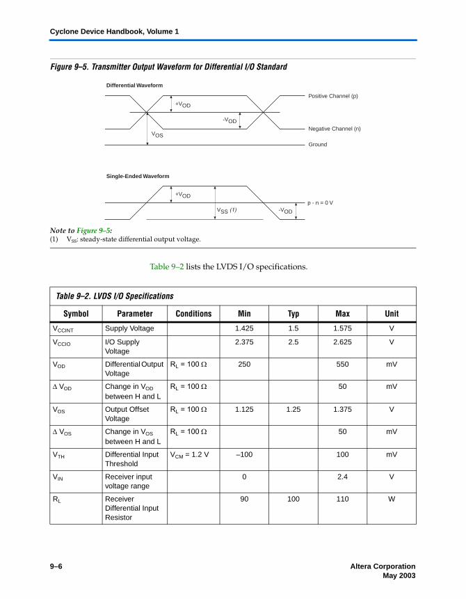
9–6 Altera CorporationPreliminary May 2003
Cyclone Device Handbook, Volume 1
Figure 9–5. Transmitter Output Waveform for Differential I/O Standard
Note to Figure 9–5: (1) VSS: steady-state differential output voltage.
Table 9–2 lists the LVDS I/O specifications.
+VOD
-VOD
VOS
Ground
Positive Channel (p)
Negative Channel (n)
Single-Ended Waveform
Differential Waveform
+VOD
-VODVSS (1)p - n = 0 V
Table 9–2. LVDS I/O Specifications
Symbol Parameter Conditions Min Typ Max Unit
VCCINT Supply Voltage 1.425 1.5 1.575 V
VCCIO I/O Supply Voltage
2.375 2.5 2.625 V
VOD Differential Output Voltage
RL = 100 Ω 250 550 mV
∆ VOD Change in VOD between H and L
RL = 100 Ω 50 mV
VOS Output Offset Voltage
RL = 100 Ω 1.125 1.25 1.375 V
∆ VOS Change in VOS between H and L
RL = 100 Ω 50 mV
VTH Differential Input Threshold
VCM = 1.2 V –100 100 mV
VIN Receiver input voltage range
0 2.4 V
RL Receiver Differential Input Resistor
90 100 110 W

Altera Corporation 9–7May 2003 Preliminary
Cyclone LVDS I/O Interface
LVDS Timing in Cyclone Devices
Since LVDS enables data transmission at very high speed, LVDS timing analysis is different than other I/O standards. You must understand how to analyze timing for the LVDS signal, which is based on skew between the data and the clock signal.
You should also consider board skew, cable skew, and clock jitter in your calculation. This section briefly explains the LVDS timing parameter in Cyclone devices.
Table 9–3 defines the parameters of the timing diagram shown in Figure 9–6.
Figure 9–6. LVDS Timing Diagram
Figure 9–7 shows the LVDS timing budget.
Table 9–3. LVDS Timing Definition
Parameter Definition Description
SW Sampling Window
Period of time input data must be stable so it can be successfully sampled by the receiver.
TCCS Channel-to-Channel Skew
Difference between the fastest and slowest data output transitions, which include clock-to-output (tCO) and clock skew of the transmitter.
RSKM Receiver Input Skew Margin
Total margin left after accounting for SW and TCCS.
Sampling Window (SW)
Time Unit Interval (TUI)
RSKM TCCSRSKMTCCS
Internal Clock
External Input Clock
Receiver Input Data

9–8 Altera CorporationPreliminary May 2003
Cyclone Device Handbook, Volume 1
Figure 9–7. Cyclone LVDS Timing Budget Note (1)
Note to Figure 9–7:(1) The equation for the LVDS timing budget is: Period = 0.5 × TCCS + RSKM + SW + RSKM + 0.5 × TCCS.
Table 9–4 shows the preliminary timing budget for Cyclone devices at 311 Mbps.
1 This application note will be updated with actual silicon data after device characterization is complete.
Cyclone Receiver & Transmitter Termination
Receiving LVDS signals on Cyclone I/O pins is straightforward, and can be done by assigning LVDS to desired pins in the Quartus II software. A 100-Ω parallel terminator is required at the receiver input pin, as shown in Figure 9–8.
Internal Clock Period
RSKM 0.5 × TCCS RSKM 0.5 × TCCSSW
Table 9–4. Preliminary Timing Budget for Cyclone LVDS at 311 Mbps
Parameter Time (ns)
Period 3.22
SW 1.20
TCCS 1.02
RSKM 0.50
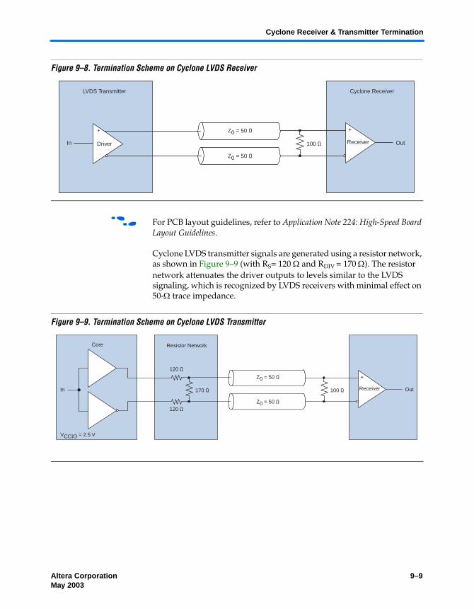
Altera Corporation 9–9May 2003 Preliminary
Cyclone Receiver & Transmitter Termination
Figure 9–8. Termination Scheme on Cyclone LVDS Receiver
f For PCB layout guidelines, refer to Application Note 224: High-Speed Board Layout Guidelines.
Cyclone LVDS transmitter signals are generated using a resistor network, as shown in Figure 9–9 (with RS= 120 Ω and RDIV = 170 Ω). The resistor network attenuates the driver outputs to levels similar to the LVDS signaling, which is recognized by LVDS receivers with minimal effect on 50-Ω trace impedance.
Figure 9–9. Termination Scheme on Cyclone LVDS Transmitter
Z0 = 50 Ω
Cyclone ReceiverLVDS Transmitter
In Out
Z0 = 50 Ω
100 Ω
+
Driver Receiver
+
Z0 = 50 Ω
Core
Out
Z0 = 50 Ω
100 Ω170 Ω Receiver
+
VCCIO = 2.5 V
120 Ω
120 Ω
Resistor Network
In

9–10 Altera CorporationPreliminary May 2003
Cyclone Device Handbook, Volume 1
Implementing Cyclone LVDS I/O Pins in the Quartus II Software
For differential signaling, the receiver must deserialize the incoming data and send it to the internal logic as a parallel signal. Accordingly, the transmitter must serialize the parallel data coming from the internal logic to send it off-chip (see Figure 9–10).
Figure 9–10. Deserialization & Serialization at Receiver & Transmitter
Although Cyclone devices do not incorporate a dedicated serializer/ deserializer (SERDES), you can incorporate these functions in your design using the Quartus II software.
Table 9–5 shows the three different reference design examples discussed in this application note.
1 Reference design examples for EP1C20, EP1C12, EP1C6, and EP1C4 devices have two PLLs per device, whereas EP1C3 devices in the 144-pin TQFP package have only one. Reference design files are listed under the title of this application note on the Altera web site at www.altera.com.
Transmitting Serial Data on Cyclone LVDS Outputs
The LVDS transmitter reference design allows the data and clock frequency to be simultaneously transmitted. Figure 9–11 shows the circuit schematic of a reference design for serialization of an 8-bit parallel bus implemented in EP1C20, EP1C12, EP1C6, and EP1C4 devices.
Table 9–5. Reference Designs
PLL Mode Input Clock Frequency (MHz)
×2 155.50
×4 77.75
×8 38.88
Cyclone Device
Deserializer Serializer
rxin +
rxin -
txout +
txout -
Serial DataSerial Data
Receiver Transmitter

Altera Corporation 9–11May 2003 Preliminary
Implementing Cyclone LVDS I/O Pins in the Quartus II Software
Figure 9–12 shows the × 8 mode serialization circuitry implementation in EP1C3 devices. You can modify reference designs for desired serialization.
Figure 9–11. Reference Design Schematic for × 8 Mode Serializer Implemented for EP1C20, EP1C12 & EP1C6 Devices

9–12 Altera CorporationPreliminary May 2003
Cyclone Device Handbook, Volume 1
Figure 9–12. Reference Design Schematic for × 8 Mode Serializer Implemented for EP1C3 Devices (144-Pin TQFP Package)
In Figures 9–11 and 9–12, the D-type flipflops (D_FF) are used to register the parallel data, and a Cyclone PLL is used to multiply the core logic clock frequency. Cyclone PLLs provide clock synthesis for PLL output ports using M/(N × post- scalar) scaling factors. A shift register is used to convert the parallel-to-serial data stream, and a counter and a comparator are used to determine the byte boundary.

Altera Corporation 9–13May 2003 Preliminary
Implementing Cyclone LVDS I/O Pins in the Quartus II Software
Transmitter Circuit
The input and output signals and their function in the sample transmitter design are listed in Tables 9–6 and 9–7.
Table 9–8 lists the modules used in the circuit and their corresponding functions or purpose.
Table 9–6. LVDS Input Pins (LVDS_TX)
Pin Description
data[7..0] 8 bits of parallel inputs.
clk PLL input clock. If ×8 mode is used, the input clock frequency is 38.88 MHz; for ×4 mode, the input frequency is 77.75 MHz; and for ×2 mode, the input frequency is 155.5 MHz.
reset Active-high reset signal. This pin is driven high at the beginning of operation.
Table 9–7. LVDS Output Pins (LVDS_TX)
Pin Description
dataout The data rate is 311 Mbps.
clkout You can choose whether to have a fast clock as the clock out (311 MHz), or a slow clock as the clock out (38.88 MHz for ×8 mode, 77.75 MHz for ×4 mode, or 155.5 MHz for ×2 mode). The frequency is dependent on the input clock frequency required on the receiver of the transmitted data. The clock out frequency in this reference design is 311 MHz. Modify the design if another output clock frequency is desired.
Table 9–8. Transmitter Circuit Modules (Part 1 of 2)
Module Description
PARALLEL_REG Consists of eight registers, each is connected to one bit of data input. The slow clock from the PLL is used to register the data.
PLL Input of the PLL is the input clk signal. In the ×8 mode design, the frequency is 38.88 MHz. Therefore, the PLL outputs are c0 at 311 MHz and c1 at 38.88 MHz. If needed, you can use the PLL locked signal.
SHIFT_REG This parallel-in-serial-out SHIFT_REG acts as a serializer. The PLL output c0 clocks SHIFT_REG at 311 MHz. Consequently, the serial output of the shift register can be transmitted at 311 Mbps. The best location for the shift register is the logic array block (LAB) adjacent to the dataout pin.

9–14 Altera CorporationPreliminary May 2003
Cyclone Device Handbook, Volume 1
Capturing Serial Data on Cyclone LVDS Inputs
Cyclone devices do not incorporate a dedicated deserializer to capture the serial stream data and clock. However, you can design a deserializer using the Quartus II software. Figure 9–13 shows a reference design for a deserializer circuit implemented in EPC1C20, EP1C12, EP1C6, and EP1C4 devices. Figure 9–14 shows the × 8 mode deserializer circuitry implemented in EP1C3 devices.
Figure 9–13. Reference Design Schematic for Receiver Deserializer Implemented in EP1C20, EP1C12, EP1C6 & EP1C4 Devices
COUNTER The counter is enabled after the first rising edge of the slow clock c1. The counter and comparator are used to determine the byte boundary.
COMPARE7 COMPARE7 is a comparator. When the input of COMPARE7 is d'7, it will drive out high. The output of COMPARE7 is the load signal of the parallel-in-serial-out shift register.
D_FF To register the data before driving off chip, use the register in the input/output element (IOE) of the output pin.
CTR_8 This counter is used in EP1C3 devices only. Since EP1C3 devices have only one PLL, this counter is used as a divider to produce the slow clock c1.
Table 9–8. Transmitter Circuit Modules (Part 2 of 2)
Module Description

Altera Corporation 9–15May 2003 Preliminary
Implementing Cyclone LVDS I/O Pins in the Quartus II Software
Figure 9–14. Reference Design Schematic for Receiver Deserializer Implemented in EP1C3 Devices
Receiver Circuit
The input and output signals and their function in a sample receiver design are listed in Tables 9–9 and 9–10.
Table 9–9. LVDS Input Pins (LVDS_RX)
Pin Description
data_i Incoming serial stream of data.
clk PLL input clock. If ×8 mode is used, the input clock frequency is 38.88 MHz; for ×4 mode, the input frequency is 77.75 MHz; and for ×2 mode, the input frequency is 155.5 MHz.
reset Active-high reset signal. This pin is driven high at the beginning of operation.
Table 9–10. LVDS Output Pins (LVDS_RX)
Pin Description
out_rx[7..0] Output bus (8 bits in ×8 mode).
c1/clkdiv8 Slower PLL output clock which goes to internal logic. If ×8 mode is used, the input clock frequency is 38.88 MHz; for ×4 mode, the input frequency is 77.75 MHz; and for ×2 mode, the input frequency is 155.5 MHz.

9–16 Altera CorporationPreliminary May 2003
Cyclone Device Handbook, Volume 1
Table 9–11 lists the modules used in the circuit and their corresponding functions or purpose.
Design Guidelines
To implement LVDS in Cyclone devices, adhere to the following design guidelines in the Quartus II software.
Route LVDS CLKOUT to pins through regular user LVDS pins. This routing provides better TCCS margin.
To meet the tSU and tCO timing requirement between serial and parallel registers, use the I/O registers of the input and output pins.
fMAX is limited by the delay between the IOE and the next logic element (LE) register. To achieve an fMAX of 311 MHz, the delay between the IOE and the next LE register at the receiver and transmitter side must not be more than 3.215 ns.
The best location to implement the shift registers is within the LAB adjacent to the input or output pin.
LVDS data and clock should be aligned at the output pin. If these signals are not aligned, use a phase shift to align them.
1 The Cyclone LVDS reference design did not need this delay since the delay between LVDS clock and data at the pin was negligible.
Table 9–11. Receiver Circuit Modules
Module Description
D_FF Captures the incoming serial stream data. PLL output c0 (311 MHz) is inverted to sample the LVDS receiver data in the middle of the data eye. The register is placed in the IOE of the data_i pin.
PLL Input of the PLL is the input clk signal. PLL output c0 (311 MHz) clocks SHIFT_REG and the inverted c0 clocks D_FF. PLL output c1 (38.88 MHz) provides the clock for PARALLEL_REG.
SHIFT_REG Serial-in-parallel-out shift register. Consists of eight D_FF modules. Converts the serial data from 311 Mbps to eight bits of parallel data clocked at 38.88 MHz. The best location for the shift register is the LAB adjacent to the data_i pin.
PARALLEL_REG Consists of eight registers, each is connected to one bit of data input. The slow clock from the PLL (c1) is used to clock the parallel register.
CTR_8 This counter is used in only EP1C3 devices. Since EP1C3 devices have only one PLL, this counter is used as a divider to produce the slow clock.

Altera Corporation 9–17May 2003 Preliminary
Design Guidelines
Differential Pad Placement Guidelines
To maintain an acceptable noise level on the VCCIO supply, there are restrictions on placement of single-ended I/O pins in relation to differential pads. Refer to the guidelines in Chapter 8, Using Selectable I/O Standards in Cyclone Devices for placing single-ended pads with respect to differential pads in Cyclone devices.
Board Design Considerations
This section explains how to get the optimal performance from the Cyclone I/O block and ensure first-time success in implementing a functional design with optimal signal quality. The critical issues of controlled impedance of traces and connectors, differential routing, and termination techniques must all be considered to get the best performance from the integrated circuit (IC). Use this application note together with Section I, Cyclone FPGA Family Data Sheet.
The Cyclone device generates signals that travel over the media at frequencies as high as 311 Mbps. Use the following general guidelines:
Base board designs on controlled differential impedance. Calculate and compare all parameters such as trace width, trace thickness, and the distance between two differential traces.
Maintain equal distance between traces in LVDS pairs, as much as possible. Routing the pair of traces close to each other will maximize the common-mode rejection ratio (CMRR)
Longer traces have more inductance and capacitance. These traces should be as short as possible to limit signal integrity issues.
Place termination resistors as close to receiver input pins as possible.
Use surface mount components.
Avoid 90° or 45° corners.
Use high-performance connectors.
Design backplane and card traces so that trace impedance matches the connector’s and/or the termination’s impedance.
Keep equal number of vias for both signal traces.

9–18 Altera CorporationPreliminary May 2003
Cyclone Device Handbook, Volume 1
Create equal trace lengths to avoid skew between signals. Unequal trace lengths result in misplaced crossing points and decrease system margins as the TCCS value increases.
Limit vias because they cause discontinuities.
Use the common bypass capacitor values such as 0.001 µF, 0.01 µF, and 0.1 µF to decouple the high-speed PLL power and ground planes.
Keep switching TTL signals away from differential signals to avoid possible noise coupling.
Do not route TTL clock signals to areas under or above the differential signals.
Analyze system-level signals.
Conclusion Cyclone LVDS I/O capabilities enable you to keep pace with increasing design complexity while offering the lowest-cost FPGA on the market. Support for I/O standards including LVDS allows Cyclone devices to fit into a wide variety of applications. Taking advantage of these I/O standards and Cyclone pricing allows you to lower your design costs while remaining on the cutting edge of technology.

Altera Corporation Section V–1Preliminary
Section V. DesignConsiderations
This section provides documentation on design considerations when utilizing Cyclone devices. In addition to these design considerations, refer to the Intellectual Property section of the Altera web site for a complete offering of IP cores for Cyclone devices.
This section contains the following chapters:
Chapter 10. Implementing Double Data Rate I/O Signaling in Cyclone Devices
Chapter 11. Using Cyclone Devices in Multiple-Voltage Systems
Chapter 12. Designing with 1.5-V Devices
Revision History The table below shows the revision history for Chapter 10 and 11.
Chapter(s) Date / Version Changes Made
10 May 2003v1.0
Updated text under Figure 10–3.
11 May 2003v1.0
Initial release.
12 May 2003v1.0
Initial handbook release.

Section V–2 Altera CorporationPreliminary
Design Considerations Cyclone Device Handbook, Volume 1

Altera Corporation 10–1May 2003 Preliminary
10. Implementing DoubleData Rate I/O Signaling in
Cyclone Devices
Introduction Double data rate (DDR) transmission is used in many applications where fast data transmission is needed, such as memory access and first-in first-out (FIFO) memory structures. DDR uses both edges of a clock to transmit data, which facilitates data transmission at twice the rate of a single data rate (SDR) architecture using the same clock speed. This method also reduces the number of I/O pins required to transmit data.
This application note shows implementations of a double data rate I/O interface using CycloneTM devices. Cyclone devices support DDR input, DDR output, and bidirectional DDR signaling.
f For more information on using Cyclone devices in applications with DDR SDRAM and FCRAM memory devices, see “DDR Memory Support” on page 10–4.
Double Data Rate Input
The DDR input implementation shown in Figure 10–1 uses four internal logic element (LE) registers located in the logic array block (LAB) adjacent to the DDR input pin. The DDR data is fed to the first two of four registers. One register captures the DDR data present during the rising edge of the clock. The second register captures the DDR data present during the falling edge of the clock.
Figure 10–1. Double Data Rate Input Implementation
n_edge_reg
PRND Q
PRND Q
PRND Q
PRND Q
p_edge_reg
ddr_l_sync_reg
ddr_h_sync_reg
ddr
clk
ddr_out_l
ddr_out_h
NOT
DFF
DFF
DFF
DFF
C51010-1.0

10–2 Altera CorporationPreliminary May 2003
Cyclone Device Handbook, Volume 1
The third and fourth registers synchronize the two data streams to the rising edge of the clock. Figure 10–2 shows examples of functional waveforms from a double data rate input implementation.
Figure 10–2. Double Data Rate Input Functional Waveforms
Double Data Rate Output
Figure 10–3 shows a schematic representation of double data rate output implemented in a Cyclone device. The DDR output logic is implemented using LEs in the LAB adjacent to the output pin. Two registers are used to synchronize two serial data streams. The registered outputs are then multiplexed by the common clock to drive the DDR output pin at two times the data rate.
Figure 10–3. Double Data Rate Output Implementation
While the clock signal is logic-high, the output from reg_h is driven onto the DDR output pin. While the clock signal is logic-low, the output from reg_l is driven onto the DDR output pin. The DDR output pin can be any available user I/O pin.
Figure 10–4 shows examples of functional waveforms from a double data rate output implementation.
clk
ddr
ddr_out_h
ddr_out_l
data_in_h
clk
ddr
PRND Q
PRND Qdata_in_l
data1
data0
sel
result
reg_l
reg_h
DFF
DFF

Altera Corporation 10–3May 2003 Preliminary
Bidirectional Double Data Rate
Figure 10–4. Double Data Rate Output Waveforms
Bidirectional Double Data Rate
Figure 10–5 shows a bidirectional DDR interface, constructed using the DDR input and DDR output examples described in the previous two sections. As with the DDR input and DDR output examples, the bidirectional DDR pin can be any available user I/O pin, and the registers used to implement DDR bidirectional logic are LEs in the LAB adjacent to that pin. The tri-state buffer (TRI) controls when the device drives data onto the bidirectional DDR pin.
Figure 10–5. Bidirectional Double Data Rate Implementation
clk
ddr
data_in_l
data_in_h
clk
PRND Q
PRND Q
data1
data0
sel
result
PRNDQ
PRNDQ
PRNDQ
PRNDQ
ddr_out_h
ddr_out_l
ddr_in_l
ddr_in_h
ddr
ddr_wen
NOT
DFF DFF
DFF DFF
DFF
DFF
TRI

10–4 Altera CorporationPreliminary May 2003
Cyclone Device Handbook, Volume 1
Figure 10–6 shows example waveforms from a bidirectional double data rate implementation.
Figure 10–6. Double Data Rate Bidirectional Waveforms
DDR Memory Support
The Cyclone device family supports both DDR SDRAM and FCRAM memory interfaces up to 133 MHz.
f For more information on extended DDR memory support in Cyclone devices, see Section I, Cyclone FPGA Family Data Sheet.
Conclusion Utilizing both the rising and falling edges of a clock signal, double data rate transmission is a popular strategy for increasing the speed of data transmission while reducing the required number of I/O pins. Cyclone devices can be used to implement this strategy for use in applications such as FIFO structures, SDRAM/FCRAM interfaces, as well as other time-sensitive memory access and data-transmission situations.
data_out_h
data_out_l
ddr~result
clk
data_in_h
data_in_l
ddr_wen
ddr

Altera Corporation 11–1May 2003 Preliminary
11. Using Cyclone Devices inMultiple-Voltage Systems
Introduction To meet the demand for higher system speed in data communications, semiconductor vendors use increasingly advanced processing technologies requiring lower operating voltages. As a result, printed circuit boards (PCBs) often incorporate devices conforming to one of several voltage level I/O standards, such as 3.3-V, 2.5-V, 1.8-V and 1.5-V. A mixture of components with various voltage level I/O standards on a single PCB is inevitable.
In order to accommodate this mixture of devices on a single PCB, a device that can act as a bridge or interface between these devices is needed. The Cyclone™ device family’s MultiVolt™ I/O operation capability meets the increasing demand for compatibility with devices of different voltages. MultiVolt I/O operation separates the power supply voltage from the output voltage, enabling Cyclone devices to interoperate with other devices using different voltage levels on the same PCB.
In addition to MultiVolt I/O operation, this application note discusses several other features that allow you to use Cyclone devices in multiple-voltage systems without damaging the device or the system, including:
Hot-Socketing—add and remove Cyclone devices to and from a powered-up system without affecting the device or system operation
Power-Up Sequence flexibility—Cyclone devices can accommodate any possible power-up sequence
Power-On Reset—Cyclone devices maintain a reset state until voltage is within operating range
I/O Standards The I/O buffer of a Cyclone device is programmable and supports a wide range of I/O voltage standards. Each I/O bank in a Cyclone device can be programmed to comply with a different I/O standard. All I/O banks can be configured with the following I/O standards:
3.3-V LVTTL/LVCMOS 2.5-V LVTTL/LVCMOS 1.8-V LVTTL/LVCMOS 1.5-V LVCMOS LVDS SSTL-2 Class I and II SSTL-3 Class I and II
C51011-1.0
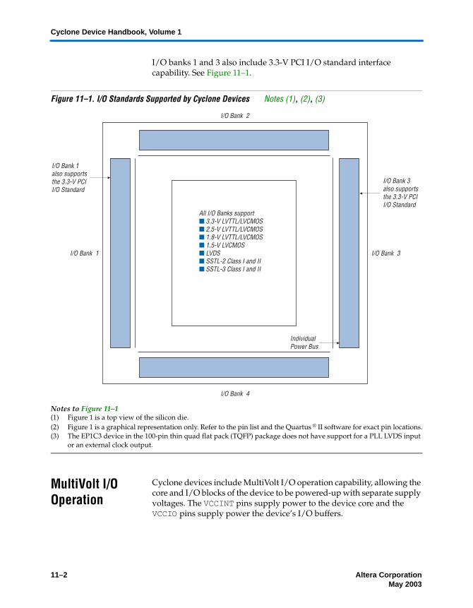
11–2 Altera CorporationPreliminary May 2003
Cyclone Device Handbook, Volume 1
I/O banks 1 and 3 also include 3.3-V PCI I/O standard interface capability. See Figure 11–1.
Figure 11–1. I/O Standards Supported by Cyclone Devices Notes (1), (2), (3)
Notes to Figure 11–1(1) Figure 1 is a top view of the silicon die.(2) Figure 1 is a graphical representation only. Refer to the pin list and the Quartus ® II software for exact pin locations.(3) The EP1C3 device in the 100-pin thin quad flat pack (TQFP) package does not have support for a PLL LVDS input
or an external clock output.
MultiVolt I/O Operation
Cyclone devices include MultiVolt I/O operation capability, allowing the core and I/O blocks of the device to be powered-up with separate supply voltages. The VCCINT pins supply power to the device core and the VCCIO pins supply power the device’s I/O buffers.
I/O Bank 1
I/O Bank 2
I/O Bank 3
I/O Bank 4
I/O Bank 1 also supports the 3.3-V PCI I/O Standard
I/O Bank 3 also supports the 3.3-V PCI I/O Standard
All I/O Banks support 3.3-V LVTTL/LVCMOS 2.5-V LVTTL/LVCMOS 1.8-V LVTTL/LVCMOS 1.5-V LVCMOS LVDS SSTL-2 Class I and II SSTL-3 Class I and II
Individual Power Bus

Altera Corporation 11–3May 2003 Preliminary
5.0-V Device Compatibility
1 Supply all device VCCIO pins that have MultiVolt I/O capability at the same voltage level (e.g., 3.3-V, 2.5-V, 1.8-V, or 1.5-V). See Figure 11–2.
Figure 11–2. Implementing a Multiple-Voltage System with a Cyclone Device
5.0-V Device Compatibility
A Cyclone device may not correctly interoperate with a 5.0-V device if the output of the Cyclone device is connected directly to the input of the 5.0-V device. If VOUT of the Cyclone device is greater than VCCIO, the PMOS pull-up transistor still conducts if the pin is driving high, preventing an external pull-up resistor from pulling the signal to 5.0-V.
A Cyclone device can drive a 5.0-V LVTTL device by connecting the VCCIO pins of the Cyclone device to 3.3 V. This is because the output high voltage (VOH) of a 3.3-V interface meets the minimum high-level voltage of 2.4-V of a 5.0-V LVTTL device. (A Cyclone device cannot drive a 5.0-V LVCMOS device.)
Because the Cyclone devices are 3.3-V, 32-bit, 66 MHz PCI compliant the input circuitry accepts a maximum high-level input voltage (VIH) of 4.1-V. To drive a Cyclone device with a 5.0-V device, you must connect a resistor (R2) between the Cyclone device and the 5.0-V device. See Figure 11–3.
CycloneDevice
3.3-VDevice
2.5-VDevice
5.0-VDevice

11–4 Altera CorporationPreliminary May 2003
Cyclone Device Handbook, Volume 1
Figure 11–3. Driving a Cyclone Device with a 5.0-Volt Device
If VCCIO is between 3.0-V and 3.6-V and the PCI clamping diode is enabled, the voltage at point B in Figure 11–3 is 4.3-V or less. To limit large current draw from the 5.0-V device, R2 should be small enough for a fast signal rise time and large enough so that it does not violate the high-level output current (IOH) specifications of the devices driving the trace. The PCI clamping diode in the Cyclone device can support 25mA of current.
To compute the required value of R2, first calculate the model of the pull-up transistors on the 5.0-V device. This output resistor (R1) can be modeled by dividing the 5.0-V device supply voltage (VCC) by the IOH: R1 = VCC/IOH.
Figure 11–4 shows an example of typical output drive characteristics of a 5.0-V device.
VCC
R2I I
5.0 V ± 0.25 V
Model as R1
5.0-V DeviceCyclone Device
VCCIO
VCCIO
3.0 - 3.4 V ± 0.25 V
PCI Clamp
B

Altera Corporation 11–5May 2003 Preliminary
5.0-V Device Compatibility
Figure 11–4. Output Drive Characteristics of a 5.0-V Device
As shown above, R1 = 5.0-V/135 mA.
1 The values usually shown in data sheets reflect typical operating conditions. Subtract 20% from the data sheet value for guard band. This subtraction applied to the above example gives R1 a value of 30 Ω.
R2 should be selected to not violate the driving device’s IOH specification. For example, if the above device has a maximum IOH of 8 mA, given the PCI clamping diode, VIN = VCCIO + 0.7-V = 3.7-V. Given that the maximum supply load of a 5.0-V device (VCC) will be 5.25-V, the value of R2 can be calculated as follows:
This analysis assumes worst-case conditions. If your system will not see a wide variation in voltage-supply levels, you can adjust these calculations accordingly.
1 Because 5.0-V device tolerance in Cyclone devices requires use of the PCI clamp, and this clamp is activated during configuration, 5.0-V signals may not be driven into the device until it is configured.
150
90
54321
30
60
120
135
VO Output Voltage (V)
Typical Output Current (mA)
IO
IOH
IOL
VCCINT = 5.0V
VCCIO = 5.0V
R25.25V 3.7 V–( ) 8 mA 30 Ω×( )–
8 mA-------------------------------------------------------------------------------------- 164 Ω= =

11–6 Altera CorporationPreliminary May 2003
Cyclone Device Handbook, Volume 1
Hot-Socketing Hot-socketing, also known as hot-swapping, refers to inserting or removing a board or device into or out of a system board while system power is on. For a system to support hot-socketing, plug-in or removal of the subsystem or device must not damage the system or interrupt system operation.
All devices in the Cyclone family are designed to support hot-socketing without special design requirements. The following features have been implemented in Cyclone devices to facilitate hot-socketing:
Devices can be driven before power-up with no damage to the device.
I/O pins remain tri-stated during power-up. Signal pins do not drive the VCCIO or VCCINT power supplies.
1 Because 5.0-V tolerance in Cyclone devices require the use of the PCI clamping diode, and the clamping diode is only available after configuration has finished, be careful not to connect 5.0-V signals to the device.
Devices Can Be Driven before Power-Up
The device I/O pins, dedicated input pins, and dedicated clock pins of Cyclone devices can be driven before or during power-up without damaging the devices.
I/O Pins Remain Tri-Stated during Power-Up
A device that does not support hot-socketing may interrupt system operation or cause contention by driving out before or during power-up. For Cyclone devices, I/O pins are tri-stated before and during power-up and configuration, and will not drive out.
Signal Pins Do Not Drive the VCCIO or VCCINT Power Supplies
A device that does not support hot-socketing will short power supplies together when powered-up through its signal pins. This irregular power-up can damage both the driving and driven devices and can disrupt card power-up.
In Cyclone devices, there is no current path from I/O pins, dedicated input pins, or dedicated clock pins to the VCCIO or VCCINT pins before or during power-up. A Cyclone device may be inserted into (or removed from) a powered-up system board without damaging or interfering with system-board operation. When hot-socketing, Cyclone devices have a minimal effect on the signal integrity of the backplane.
Altera Corporation 11–7May 2003 Preliminary
Power-Up Sequence
1 The maximum DC current when hot-socketing Cyclone devices is less than 300 µA, whereas the maximum AC current during hot-socketing is less than 8 mA for a period of 10ns or less.
During hot-socketing, the signal pins of a device may be connected and driven by the active system before the power supply can provide current to the device VCC and ground planes. Known as latch-up, this condition can cause parasitic diodes to turn on within the device, causing the device to consume a large amount of current, and possibly causing electrical damage. This operation can also cause parasitic diodes to turn on inside of the driven device. Cyclone devices are immune to latch-up when hot-socketing.
Power-Up Sequence
Because Cyclone devices can be used in a multi-voltage environment, they are designed to tolerate any possible power-up sequence. Either VCCINT or VCCIO can initially supply power to the device, and 3.3-V, 2.5-V, 1.8-V, or 1.5-V input signals can drive the devices without special precautions before VCCINT or VCCIO is applied. Cyclone devices can operate with a VCCIO voltage level that is higher than the VCCINT level. You can also change the VCCIO supply voltage while the board is powered-up. However, you must ensure that the VCCINT and VCCIO power supplies stay within the correct device operating conditions.
When VCCIO and VCCINT are supplied from different power sources to a Cyclone device, a delay between VCCIO and VCCINT may occur. Normal operation does not occur until both power supplies are in their recommended operating range. When VCCINT is powered-up, the IEEE Std. 1149.1 Joint Test Action Group (JTAG) circuitry is active. If TMS and TCK are connected to VCCIO and VCCIO is not powered-up, the JTAG signals are left floating. Thus, any transition on TCK can cause the state machine to transition to an unknown JTAG state, leading to incorrect operation when VCCIO is finally powered-up. To disable the JTAG state during the power-up sequence, TCK should be pulled low to ensure that an inadvertent rising edge does not occur on TCK.
Power-On Reset When designing a circuit, it is important to consider system state at power-up. Cyclone devices maintain a reset state during power-up. When power is applied to a Cyclone device, a power-on-reset event occurs if VCC reaches the recommended operating range within a certain period of time (specified as a maximum VCC rise time). A POR event does not occur if these conditions are not met because slower rise times can cause incorrect device initialization and functional failure.

11–8 Altera CorporationPreliminary May 2003
Cyclone Device Handbook, Volume 1
1 If VCCINT does not remain in the specified operating range, operation is not assured until VCCINT re-enters the range.
Conclusion PCBs often contain a mix of 5.0-V, 3.3-V, 2.5-V, 1.8-V, and 1.5-V devices. The Cyclone device family’s MultiVolt I/O operation capability allows you to incorporate newer-generation devices with devices of varying voltage levels. This capability also enables the device core to run at its core voltage, VCCINT, while maintaining I/O pin compatibility with other logic levels. Altera has taken further steps to make system design easier by designing devices that allow VCCINT and VCCIO to power-up in any sequence and by incorporating support for hot-socketing.

Altera Corporation 12–1May 2003 Preliminary
12. Designing with1.5-V Devices
Introduction The CycloneTM FPGA family provides the best solution for high-volume, cost-sensitive applications. Similar to StratixTM devices, Cyclone devices are fabricated on a leading-edge 1.5-V, 0.13-µm, all-layer copper SRAM process.
Using a 1.5-V operating voltage provides the following advantages:
Lower power consumption compared to 2.5-V or 3.3-V devices. Lower operating temperature. Less need for fans and other temperature-control elements.
Since many existing designs are based on 5.0-V, 3.3-V and 2.5-V power supplies, a voltage regulator may be required to lower the voltage supply level to 1.5-V. This application note provides guidelines for designing with Cyclone devices in mixed-voltage and single-voltage systems and provides examples using voltage regulators. This application note also includes information on:
Power Sequencing & Hot Socketing Using MultiVolt I/O Pins Voltage Regulators 1.5-V Regulator Application Examples Board Layout Power Sequencing & Hot Socketing
Power Sequencing & Hot Socketing
Because 1.5-V Cyclone FPGAs can be used in a mixed-voltage environment, they have been designed specifically to tolerate any possible power-up sequence. Therefore, the VCCIO and VCCINT power supplies may be powered in any order.
You can drive signals into Cyclone FPGAs before and during power up without damaging the device. In addition, Cyclone FPGAs do not drive out during power up since they are tri-stated during power up. Once the device reaches operating conditions and is configured, Cyclone FPGAs operate as specified by the user.
f See the Cyclone Field Programmable Gate Array Family Data Sheet for more information.
C51012-1.0

12–2 Altera CorporationPreliminary May 2003
Cyclone Device Handbook, Volume 1
Using MultiVolt I/O Pins
Cyclone FPGAs require a 1.5-V VCCINT and a 3.3-V, 2.5-V, 1.8-V, or 1.5-V I/O supply voltage level (VCCIO). All pins, including dedicated inputs, clock, I/O, and JTAG pins, are 3.3-V tolerant before and after VCCINT and VCCIO are powered.
When VCCIO is connected to 1.5-V, the output is compatible with 1.5-V logic levels. The output pins can be made 1.8-V, 2.5-V, or 3.3-V compatible by using open-drain outputs pulled up with external resistors. You can use external resistors to pull open-drain outputs up with a 1.8-V, 2.5-V, or 3.3-V VCCIO. Table 12–1 summarizes Cyclone MultiVolt I/O support.
Figure 12–1 shows how Cyclone FPGAs interface with 3.3--V and 2.5-V devices while operating with a 1.5-V VCCINT to increase performance and save power.
Table 12–1. Cyclone MultiVolt I/O Support Note (1)
VCCIO (V)Input Signal Output Signal
1.5-V 1.8-V 2.5-V 3.3-V 5.0-V 1.5-V 1.8-V 2.5-V 3.3-V 5.0-V
1.5-V v v v (2) v (2) v
1.8-V v v v v (3) v
2.5-V v v v (5) v (5) v
3.3-V v (4) v v (6) v (7) v (7) v (7) v v (8)
Notes to Table 12–1:(1) The PCI clamping diode must be disabled to drive an input with voltages higher than VCCIO.(2) When VCCIO = 1.5-V and a 2.5-V or 3.3-V input signal feeds an input pin, higher pin leakage current is expected.(3) When VCCIO = 1.8-V, a Cyclone device can drive a 1.5-V device with 1.8-V tolerant inputs.(4) When VCCIO = 3.3-V and a 2.5-V input signal feeds an input pin, the VCCIO supply current will be slightly larger
than expected.(5) When VCCIO = 2.5-V, a Cyclone device can drive a 1.5-V or 1.8-V device with 2.5-V tolerant inputs.(6) Cyclone devices can be 5.0-V tolerant with the use of an external resistor and the internal PCI clamp diode.(7) When VCCIO = 3.3-V, a Cyclone device can drive a 1.5-V, 1.8-V, or 2.5-V device with 3.3-V tolerant inputs.(8) When VCCIO = 3.3-V, a Cyclone device can drive a device with 5.0-V LVTTL inputs but not 5.0-V LVCMOS inputs.

Altera Corporation 12–3May 2003 Preliminary
Voltage Regulators
Figure 12–1. Cyclone FPGAs Interface with 3.3-V & 2.5-V Devices
Voltage Regulators
This section explains how to generate a 1.5-V supply from another system supply. Supplying power to the 1.5-V logic array and/or I/O pins requires a 5.0-V- or 3.3-V-to-1.5-V voltage regulator. A linear regulator is ideal for low-power applications because it minimizes device count and has acceptable efficiency for most applications. A switching voltage regulator provides optimal efficiency. Switching regulators are ideal for high-power applications because of their high efficiency.
This section will help you decide which regulator to use in your system, and how to implement the regulator in your design. There are several companies that provide voltage regulators for low-voltage devices, such as Linear Technology Corporation, Maxim Integrated Products, Intersil Corporation (Elantec), and National Semiconductor Corporation.
Table 12–2 shows the terminology and specifications commonly encountered with voltage regulators. Symbols are shown in parentheses. If the symbols are different for linear and switching regulators, the linear regulator symbol is listed first.
3.3 V
2.5 V
1.5 V
3.3-V TTL
3.3-V CMOS3.3-V Device 2.5-V Device
Cyclone Device
2.5-V TTL
2.5-V CMOSVCCINT = 1.5 V
VCCIO1 = 2.5 VVCCIO2 = 3.3 V
Table 12–2. Voltage Regulator Specifications & Terminology (Part 1 of 2)
Specification/Terminology Description
Input voltage range (VIN,VCC) Minimum and maximum input voltages define the input voltage range, which is determined by the regulator process voltage capabilities.
Line regulation (line regulation, VOUT)
Line regulation is the variation of the output voltage (VOUT) with changes in the input voltage (VIN). Error amplifier gain, pass transistor gain, and output impedance all influence line regulation. Higher gain results in better regulation. Board layout and regulator pin-outs are also important because stray resistance can introduce errors.

12–4 Altera CorporationPreliminary May 2003
Cyclone Device Handbook, Volume 1
Linear Voltage Regulators
Linear voltage regulators generate a regulated output from a larger input voltage using current pass elements in a linear mode. There are two types of linear regulators available: one using a series pass element and another using a shunt element (e.g., a zener diode). Altera recommends using series linear regulators because shunt regulators are less efficient.
Load regulation(load regulation, VOUT)
Load regulation is a variation in the output voltage caused by changes in the input supply current. Linear Technology regulators are designed to minimize load regulation, which is affected by error amplifier gain, pass transistor gain, and output impedance.
Output voltage selection Output voltage selection is adjustable by resistor voltage divider networks, connected to the error amplifier input, that control the output voltage. There are multiple output regulators that create 5.0-, 3.3-, 2.5-, 1.8- and 1.5-V supplies.
Quiescent current Quiescent current is the supply current during no-load or quiescent state. This current is sometimes used as a general term for a supply current used by the regulator.
Dropout voltage Dropout voltage is the difference between the input and output voltages when the input is low enough to cause the output to drop out of regulation. The dropout voltage should be as low as possible for better efficiency.
Current limiting Voltage regulators are designed to limit the amount of output current in the event of a failing load. A short in the load causes the output current and voltage to decrease. This event cuts power dissipation in the regulator during a short circuit.
Thermal overload protection This feature limits power dissipation if the regulator overheats. When a specified temperature is reached, the regulator turns off the output drive transistors, allowing the regulator to cool. Normal operation resumes once the regulator reaches a normal operating temperature.
Reverse current protection If the input power supply fails, large output capacitors can cause a substantial reverse current to flow backward through the regulator, potentially causing damage. To prevent damage, protection diodes in the regulator create a path for the current to flow from VOUT to VIN.
Stability The dominant pole placed by the output capacitor influences stability. Voltage regulator vendors can assist you in output capacitor selection for regulator designs that differ from what is offered.
Minimum load requirements A minimum load from the voltage divider network is required for good regulation, which also serves as the ground for the regulator’s current path.
Efficiency Efficiency is the division of the output power by the input power. Each regulator model has a specific efficiency value. The higher the efficiency value, the better the regulator.
Table 12–2. Voltage Regulator Specifications & Terminology (Part 2 of 2)
Specification/Terminology Description

Altera Corporation 12–5May 2003 Preliminary
Voltage Regulators
Series linear regulators use a series pass element (i.e., a bipolar transistor or MOSFET) controlled by a feedback error amplifier (see Figure 12–2) to regulate the output voltage by comparing the output to a reference voltage. The error amplifier drives the transistor further on or off continuously to control the flow of current needed to sustain a steady voltage level across the load.
Figure 12–2. Series Linear Regulator
Table 12–3 shows the advantages and disadvantages of linear regulators compared to switching regulators.
You can minimize the difference between the input and output voltages to improve the efficiency of linear regulators. The dropout voltage is the minimum allowable difference between the regulator’s input and output voltage.
Table 12–3. Linear Regulator Advantages & Disadvantages
Advantages Disadvantages
Requires few supporting componentsLow costRequires less board spaceQuick transient responseBetter noise and drift characteristicsNo electromagnetic interference (EMI) radiation from the switching componentsTighter regulation
Less efficient (typically 60%)Higher power dissipationLarger heat sink requirements
–+
Reference
ErrorAmplifier
VOUTVIN

12–6 Altera CorporationPreliminary May 2003
Cyclone Device Handbook, Volume 1
Linear regulators are available with fixed, variable, single, or multiple outputs. Multiple-output regulators can generate multiple outputs (e.g., 1.5- and 3.3-V outputs). If the board only has a 5.0-V power voltage supply, you should use multiple-output regulators. The logic array requires a 1.5-V power supply, and a 3.3-V power supply is required to interface with 3.3- and 5.0-V devices. However, fixed-output regulators have fewer supporting components, reducing board space and cost. Figure 12–3 shows an example of a three-terminal, fixed-output linear regulator.
Figure 12–3. Three-Terminal, Fixed-Output Linear Regulator
Adjustable-output regulators contain a voltage divider network that controls the regulator’s output. Figure 12–4 shows how you can also use a three-terminal linear regulator in an adjustable-output configuration.
Figure 12–4. Adjustable-Output Linear Regulator
Switching Voltage Regulators
Step-down switching regulators can provide 3.3-V-to-1.5-V conversion with up to 95% efficiencies. This high efficiency comes from minimizing quiescent current, using a low-resistance power MOSFET switch, and, in higher-current applications, using a synchronous switch to reduce diode losses.
Linear Regulator
IN OUT
ADJ
1.5 VVIN
Linear Regulator
IN OUT
ADJ
VIN +
C1
+VREF R1
R2
C2
IADJ
VOUT = [VREF × (1 + )] + (IADJ × R1)R1
R2

Altera Corporation 12–7May 2003 Preliminary
Voltage Regulators
Switching regulators supply power by pulsing the output voltage and current to the load. Table 12–4 shows the advantages and disadvantages of switching regulators compared to linear regulators. For more information on switching regulators, see Application Note 35: Step Down Switching Regulators from Linear Technology.
There are two types of switching regulators, asynchronous and synchronous. Asynchronous switching regulators have one field effect transistor (FET) and a diode to provide the current path while the FET is off (see Figure 12–5).
Figure 12–5. Asynchronous Switching Regulator
Synchronous switching regulators have a voltage- or current-controlled oscillator that controls the on and off time of the two MOSFET devices that supply the current to the circuit (see Figure 12–6).
Table 12–4. Switching Regulator Advantages & Disadvantages
Advantages Disadvantages
Highly efficient (typically >80%)Reduced power dissipationSmaller heat sink requirementsWider input voltage rangeHigh power density
Generates EMIComplex to designRequires 15 or more supporting componentsHigher costRequires more board space
High-FrequencyCirculating Path LOAD
Switch NodeMOSFET
VOUTVIN

12–8 Altera CorporationPreliminary May 2003
Cyclone Device Handbook, Volume 1
Figure 12–6. Voltage-Controlled Synchronous Switching Regulator
Maximum Output Current
Select an external MOSFET switching transistor (optional) based on the maximum output current that it can supply. Use a MOSFET with a low on-resistance and a voltage rating high enough to avoid avalanche breakdown. For gate-drive voltages less than 9-V, use a logic-level MOSFET. A logic-level MOSFET is only required for topologies with a controller IC and an external MOSFET.
Selecting Voltage Regulators
Your design requirements determine which voltage regulator you need. The key to selecting a voltage regulator is understanding the regulator parameters and how they relate to the design.
The following checklist can help you select the proper regulator for your design:
Do you require a 3.3-V, 2.5-V, and 1.5-V output (VOUT)? What precision is required on the regulated 1.5-V supplies (line and
load regulation)? What supply voltages (VIN or VCC) are available on the board? What voltage variance (input voltage range) is expected on VIN or
VCC? What is the maximum ICC (IOUT) required by your Altera® device? What is the maximum current surge (IOUT(MAX)) that the regulator
will need to supply instantaneously?
VIN
VOUTVoltage-ControlledOscillator (VCO)
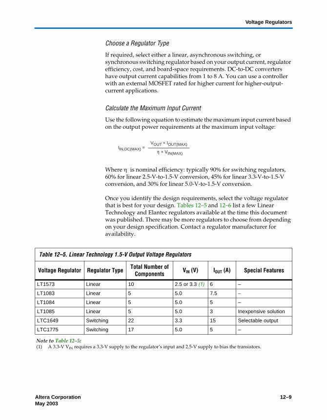
Altera Corporation 12–9May 2003 Preliminary
Voltage Regulators
Choose a Regulator Type
If required, select either a linear, asynchronous switching, or synchronous switching regulator based on your output current, regulator efficiency, cost, and board-space requirements. DC-to-DC converters have output current capabilities from 1 to 8 A. You can use a controller with an external MOSFET rated for higher current for higher-output-current applications.
Calculate the Maximum Input Current
Use the following equation to estimate the maximum input current based on the output power requirements at the maximum input voltage:
Where η is nominal efficiency: typically 90% for switching regulators, 60% for linear 2.5-V-to-1.5-V conversion, 45% for linear 3.3-V-to-1.5-V conversion, and 30% for linear 5.0-V-to-1.5-V conversion.
Once you identify the design requirements, select the voltage regulator that is best for your design. Tables 12–5 and 12–6 list a few Linear Technology and Elantec regulators available at the time this document was published. There may be more regulators to choose from depending on your design specification. Contact a regulator manufacturer for availability.
IIN,DC(MAX) =VOUT × IOUT(MAX)
η × VIN(MAX)
Table 12–5. Linear Technology 1.5-V Output Voltage Regulators
Voltage Regulator Regulator Type Total Number of Components
VIN (V) IOUT (A) Special Features
LT1573 Linear 10 2.5 or 3.3 (1) 6 –
LT1083 Linear 5 5.0 7.5 –
LT1084 Linear 5 5.0 5 –
LT1085 Linear 5 5.0 3 Inexpensive solution
LTC1649 Switching 22 3.3 15 Selectable output
LTC1775 Switching 17 5.0 5 –
Note to Table 12–5:(1) A 3.3-V VIN requires a 3.3-V supply to the regulator’s input and 2.5-V supply to bias the transistors.

12–10 Altera CorporationPreliminary May 2003
Cyclone Device Handbook, Volume 1
Voltage Divider Network
Design a voltage divider network if you are using an adjustable output regulator. Follow the controller or converter IC’s instructions to adjust the output voltage.
1.5-V Regulator Circuits
This section contains the circuit diagrams for the voltage regulators discussed in this application note. You can use the voltage regulators in this section to generate a 1.5-V power supply. Refer to the voltage regulator data sheet to find detailed specifications. If you require further information that is not shown in the data sheet, contact the regulator’s vendor.
Figures 12–7 through 12–12 show the circuit diagrams of Linear Technology voltage regulators listed in Table 12–5.
The LT1573 linear voltage regulator converts 2.5-V to 1.5-V with an output current of 6A (see Figure 12–7).
Table 12–6. Elantec 1.5-V Output Voltage Regulators
Voltage Regulator Regulator Type Total Number of Components
VIN (V) IOUT (A) Special Features
EL7551C Switching 11 5.0 1 –
EL7564CM Switching 13 5.0 4 –
EL7556BC Switching 21 5.0 6 –
EL7562CM Switching 17 3.3 or 5.5 2 –
EL7563CM Switching 19 3.3 4 –

Altera Corporation 12–11May 2003 Preliminary
Voltage Regulators
Figure 12–7. LT1573: 2.5-V-to-1.5-V/6.0-A Linear Voltage Regulator
Notes to Figure 12–7:(1) CIN1 and COUT are AVX 100-µF/10-V surface-mount tantalum capacitors.(2) Use SHDN (active high) to shut down the regulator.(3) CTIME is a 0.5-µF capacitor for 100-ms time out at room temperature.(4) CIN2 is an AVX 15-µF/10-V surface-mount tantalum capacitor.
Use adjustable 5.0- to 1.5-V regulators (shown in Figures 12–8 through 12–10) for 3.0- to 7.5-A low-cost, low-device-count, board-space-efficient solutions.
Figure 12–8. LT1083: 5.0-V-to-1.5-V/7.5-A Linear Voltage Regulator
Note to Figure 12–8:(1) This capacitor is necessary to maintain the voltage level at the input regulator.
There could be a voltage drop at the input if the voltage supply is too far away.
LT1573
FB
LATCH
SHDN (2)
GND
COMP
VOUT
VIN
DRIVE
LOAD
VOUT
R2 1k1/8 W
R1186 Ω1/8 W
CTIME0.5 µF
COUT
CIN1
MotorolaD45H11
+
+
V
3.3 VIN2
V
2.5 V
1.5 V
IN1
CIN2
+
R6 Ω1/2 W
D R200Ω
1/8 W
B
+
(1)
(4)
(3)
(1)
LT1083
ADJ
OUTIN
C1
VIN
+
C2+
R15 kΩ
R21 kΩ
10 µF10 µF
(1)
VOUT = 1.25 V × (1 + )R2
R1

12–12 Altera CorporationPreliminary May 2003
Cyclone Device Handbook, Volume 1
Figure 12–9. LT1084: 5.0-V-to-1.5-V/5.0-A Linear Voltage Regulator
Note to Figure 12–9:(1) This capacitor is necessary to maintain the voltage level at the input regulator.
There could be a voltage drop at the input if the voltage supply is too far away.
Figure 12–10. LT1085: 5.0-V-to-1.5-V/3-A Linear Voltage Regulator
Note to Figure 12–10:(1) This capacitor is necessary to maintain the voltage level at the input regulator.
There could be a voltage drop at the input if the voltage supply is too far away.
LT1083
ADJ
OUTIN
C1
VIN
+
C2+
R15 kΩ
R21 kΩ
10 µF10 µF
(1)
VOUT = 1.25 V × (1 + )R2
R1
LT1084
ADJ
OUTIN
C1
VIN
+
C2+
R15 kΩ
R21 kΩ
10 µF10 µF
(1)
VOUT = 1.25 V × (1 + )R2
R1

Altera Corporation 12–13May 2003 Preliminary
Voltage Regulators
Figure 12–11 shows a high-efficiency switching regulator circuit diagram. A selectable resistor network controls the output voltage. The resistor values in Figure 12–11 are selected for 1.5-V output operation.
Figure 12–11. LT1649: 3.3-V-to-1.5-V/15-A Asynchronous Switching Regulator
Notes to Figure 12–11:(1) MBR0530 is a Motorola device.(2) IRF7801 is a International Rectifier device.(3) Refer to the Panasonic 12TS-1R2HL device.
PVCC1
PVCC2
VCC
IMAX
SHDN
COMP
SS
GND
G1
IFB
G2
FB
VIN
C+
C–
CP OUT
LTC1649
++
+
+0.33 µF10 µF
1 µF
1 µF
1 kΩ
MBR05300.1 µF
10 µF
22 kΩ
RIMAX50 kΩ
R12.16 kΩ
R212.7 kΩ
COUT4,400 µF
VOUT1.5 V(15 A)
SHUTDOWN
MBR0530 (1)
Q3IRF7801
RC7.5 kΩ
CC0.01 µF
C1220 pF
Q1, Q2IRF7801Two inParallel (2)
CIN3,300 µF
VIN3.3 V
LEXT (3) 1.2 µH
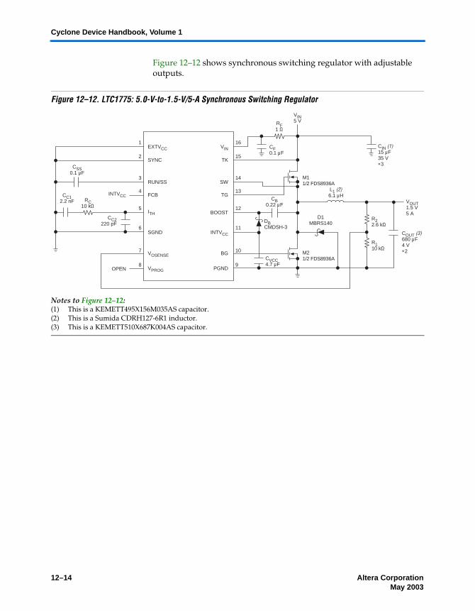
12–14 Altera CorporationPreliminary May 2003
Cyclone Device Handbook, Volume 1
Figure 12–12 shows synchronous switching regulator with adjustable outputs.
Figure 12–12. LTC1775: 5.0-V-to-1.5-V/5-A Synchronous Switching Regulator
Notes to Figure 12–12:(1) This is a KEMETT495X156M035AS capacitor.(2) This is a Sumida CDRH127-6R1 inductor.(3) This is a KEMETT510X687K004AS capacitor.
EXTVCC
ITH
VOSENSE
VPROG
SGND
SYNC
RUN/SS
FCB
VIN
BOOST
BG
PGND
INTVCC
TK
SW
TG
CC2220 pF
CC12.2 nF
INTVCC
OPEN
M11/2 FDS8936A
M21/2 FDS8936A
DBCMDSH-3
VIN5 V
VOUT1.5 V5 A
RF1 Ω
RC10 kΩ
R22.6 kΩ
R110 kΩ
CIN (1)15 µF35 V×3
COUT (3)680 µF4 V×2
CB0.22 µF
CVCC4.7 µF
CSS0.1 µF
CF0.1 µF
L1 (2)6.1 µH
D1MBRS140
1
2
3
4
5
6
7
8
16
15
14
13
12
11
10
9
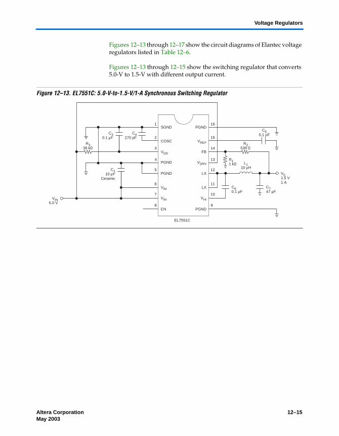
Altera Corporation 12–15May 2003 Preliminary
Voltage Regulators
Figures 12–13 through 12–17 show the circuit diagrams of Elantec voltage regulators listed in Table 12–6.
Figures 12–13 through 12–15 show the switching regulator that converts 5.0-V to 1.5-V with different output current.
Figure 12–13. EL7551C: 5.0-V-to-1.5-V/1-A Synchronous Switching Regulator
C50.1 µF
C60.1 µF
C30.1 µF
C110 µF
Ceramic
C4270 pF
C747 µF
V01.5 V1 A
VIN5.0 V
L110 µH
R2539 Ω
R339 kΩ
R11 kΩ
PGND
PGND
FB
LX
LX
VREF
VDRV
VHI
SGND
EN
VDD
PGND
VIN
COSC
PGND
VIN
EL7551C
1
2
3
4
5
6
7
8
16
15
14
13
12
11
10
9

12–16 Altera CorporationPreliminary May 2003
Cyclone Device Handbook, Volume 1
Figure 12–14. EL7564CM: 5.0-V-to-1.5-V/4-A Synchronous Switching Regulator
C30.22 µF
C50.1 µF
C4390 pF
C22.2 nF
C1330 µF
C7330 µF
V01.5 V4 A
VIN5.0 V
L14.7 µH
R422 Ω
R11 kΩ
R2539 Ω
C10100 pF
D1C6
0.22 µF
PGND
LX
PGND
PGND
VIN
STP
STN
FB
VDRV
VHI
EN
PG
LX
PGND
SGND
VDD
VTJ
VREF
COSC
PGND
EL7564CM
8
9
10
13
12
11
1
2
3
4
5
6
7
20
19
18
17
16
15
14

Altera Corporation 12–17May 2003 Preliminary
Voltage Regulators
Figure 12–15. EL7556BC: 5.0-V-to-1.5-V/6-A Synchronous Switching Regulator
Notes to Figures 12–13 − 12–15:(1) These capacitors are ceramic capacitors.(2) These capacitors are ceramic or tantalum capacitor.(3) These are BAT54S fast diodes.(4) D4 is only required for EL7556ACM.(5) This is a Sprague 293D337X96R3 2X330µF capacitor.(6) This is a Sprague 293D337X96R3 3X330µF capacitor.
C11 (2)0.22 µF
C10 (6)1.0 mF
C5 (2)1 µF
C4 (1)0.1 µF
C6 (1)0.1 µF
C8 (1)220 pF
C7 (1)39 pF
C121.0 µF
C9 (5)660 µF
VIN
TEST
PWRGD
OT
FB1
OUTEN
CSLOPE
VDD
VSSP
VSSP
VSSP
VSSP
VSSP
VCC2DET
VIN
VIN
CREF
COSC
FB2
C2V
VHI
LX
LX
VSSP
VSSP
LX
LX
CP
VSS
EL7556BC
R55.1 Ω
R4100 Ω
L12.5 µH
R639.2 Ω
R120 Ω
D4Optional (3), (4)
VOUT = 1.5 V × (1 + )
R350 Ω
VIN
D3 (3)
D2 (3)
D1 (3)
R3
R4
28
27
26
25
24
23
22
21
20
19
18
17
16
15
1
2
3
4
5
6
7
8
9
10
11
12
13
14

12–18 Altera CorporationPreliminary May 2003
Cyclone Device Handbook, Volume 1
Figures 12–16 and 12–17 show the switching regulator that converts 3.3 V to 1.5 V with different output currents.
Figure 12–16. EL7562CM: 3.3-V to 1.5-V/2-A Synchronous Switching Regulator
Figure 12–17. EL7563CM: 3.3-V to 1.5-V/4-A Synchronous Switching Regulator
VOUT1.5 V2 A
VIN3.3 V
SGND
VDD
PGND
VIN
VIN
EN
COSC
PGND
PGND
FB
LX
VHI
LX
PGND
VREF
VDRV
EL7562CM
16
15
14
13
12
11
10
9
1
2
3
4
5
6
7
8
R339 Ω
C50.1 µF
C60.1 µF
C80.1 µF
C20.1 µF
C30.1 µF
C4270 pF
C1100 µF
C90.1 µF
C7100 µF
L12.5 µH
R2539 Ω
R11 kΩ
D2 D3 D4
VOUT1.5 V4 AVIN
3.3 V
VREF
COSC
VTJ
PGND
PGND
VIN
SGND
VDD
EN
PG
VHI
LX
LX
PGND
FB
VDRV
EL7563CM
20
19
18
17
16
15
14
13
PGND
PGND
STP
STN
12
11
9
10
1
2
3
4
5
6
7
8
R422 Ω
C7330 µF
L12.5 µH
R2513 Ω
R11 kΩ
C30.22 µF
C60.22 µF
C102.2 nF
C1330 µF
C90.1 µF
C80.22 µF
C22.2 nF
C4390 pF
C50.1 µF
D1
D3
D2 D4
Altera Corporation 12–19May 2003 Preliminary
1.5-V Regulator Application Examples
1.5-V Regulator Application Examples
The following sections show the process used to select a voltage regulator for three sample designs. The regulator selection is based on the amount of power that the Cyclone device consumes. There are 14 variables to consider when selecting a voltage regulator. The following variables apply to Cyclone device power consumption:
fMAX
Output and bidirectional pins Average toggle rate for I/O pins (togIO) Average toggle rate for logic elements (LEs) (togLC) User-mode ICC consumption Maximum power-up ICCINT requirement Utilization VCCIO supply level VCCINT supply level
The following variables apply to the voltage regulator:
Output voltage precision requirement Supply voltage on the board Voltage supply output current Variance of board supply Efficiency
Different designs have different power consumptions based on the variables listed. Once you calculate the Cyclone device’s power consumption, you must consider how much current the Cyclone device needs. You can use the Cyclone power calculator (available at www.altera.com) or the PowerGaugeTM tool in the Quartus II software to determine the current needs. Also check the maximum power-up current requirement listed in the Power Consumption section of the Cyclone FPGA Family Data Sheet because the power-up current requirement may exceed the user-mode current consumption for a specific design.
Once you determine the minimum current the Cyclone device requires, you must select a voltage regulator that can generate the desired output current with the voltage and current supply that is available on the board using the variables listed in this section. An example is shown to illustrate the voltage regulator selection process.
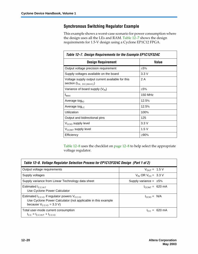
12–20 Altera CorporationPreliminary May 2003
Cyclone Device Handbook, Volume 1
Synchronous Switching Regulator Example
This example shows a worst-case scenario for power consumption where the design uses all the LEs and RAM. Table 12–7 shows the design requirements for 1.5-V design using a Cyclone EP1C12 FPGA.
Table 12–8 uses the checklist on page 12–8 to help select the appropriate voltage regulator.
Table 12–7. Design Requirements for the Example EP1C12F324C
Design Requirement Value
Output voltage precision requirement ±5%
Supply voltages available on the board 3.3 V
Voltage supply output current available for this section (II N , D C ( M A X ) )
2 A
Variance of board supply (VIN) ±5%
fMAX 150 MHz
Average togIO 12.5%
Average togLC 12.5%
Utilization 100%
Output and bidirectional pins 125
VCCIO supply level 3.3 V
VCCINT supply level 1.5 V
Efficiency ≥90%
Table 12–8. Voltage Regulator Selection Process for EP1C12F324C Design (Part 1 of 2)
Output voltage requirements VOUT = 1.5 V
Supply voltages VIN OR VCC = 3.3 V
Supply variance from Linear Technology data sheet Supply variance = ±5%
Estimated IC C I N T
Use Cyclone Power CalculatorICCINT = 620 mA
Estimated IC C I O if regulator powers VC C I O
Use Cyclone Power Calculator (not applicable in this example because VC C I O = 3.3 V)
ICCIO = N/A
Total user-mode current consumptionIC C = IC C I N T + IC C I O
ICC = 620 mA

Altera Corporation 12–21May 2003 Preliminary
Board Layout
Board Layout Laying out a printed circuit board (PCB) properly is extremely important in high-frequency (≥100 kHz) switching regulator designs. A poor PCB layout results in increased EMI and ground bounce, which affects the reliability of the voltage regulator by obscuring important voltage and current feedback signals. Altera recommends using Gerber files pre-designed layout files supplied by the regulator vendor for your board layout.
If you cannot use the supplied layout files, contact the voltage regulator vendor for help on re-designing the board to fit your design requirements while maintaining the proper functionality.
Altera recommends that you use separate layers for signals, the ground plane, and voltage supply planes. You can support separate layers by using multi-layer PCBs, assuming you are using two signal layers.
EP1C12 maximum power-up current requirementSee Power Consumption section of the Cyclone FPGA Family Data Sheet for other densities
IP U C ( M A X ) = 900 mA
Maximum output current requiredCompare IC C with IP U C ( M A X )
IO U T ( M A X ) = 900 mA
Voltage regulator selectionSee Linear Technology LTC 1649 data sheet See Intersil (Elantec) EL7562C data sheet
LTC1649 IO U T ( M A X ) =EL7562C IO U T ( M A X ) =
15 A2 A
LTC1649
Nominal efficiency (η ) Nominal efficiency (η ) = > 90%
Line and load regulationLine regulation + load regulation = (0.17 mV + 7 mV)/ 1.5 V × 100%
Line and LoadRegulation = 0.478% < 5%
Minimum input voltage (VIN(MIN))(VIN(MIN)) = VIN(1 – ∆VIN) = 3.3V(1 – 0.05) (VIN(MIN)) = 3.135 V
Maximum input currentIIN, DC(MAX) = (VOUT × IOUT(MAX))/(η × VIN(MIN))
IIN, DC(MAX) = 478 mA < 2 A
EL7562C
Nominal efficiency (η ) Nominal efficiency (η ) = > 95%
Line and load regulationLine regulation + load regulation = (0.17 mV + 7 mV)/ 1.5 V × 100%
Line and LoadRegulation = 0.5% < 5%
Minimum input voltage (VIN(MIN))(VIN(MIN)) = VIN(1 – ∆VIN) = 3.3V(1 – 0.05)
(VIN(MIN)) = 3.135 V
Maximum input currentIIN, DC(MAX) = (VOUT × IOUT(MAX))/(η × VIN(MIN))
IIN, DC(MAX) = 453 mA < 2 A
Table 12–8. Voltage Regulator Selection Process for EP1C12F324C Design (Part 2 of 2)

12–22 Altera CorporationPreliminary May 2003
Cyclone Device Handbook, Volume 1
Figure 12–18 shows how to use regulators to generate 1.5-V and 2.5-V power supplies if the system needs two power supply systems. One regulator is used for each power supply.
Figure 12–18. Two Regulator Solution for Systems that Require 5.0-V, 2.5-V & 1.5-V Supply Levels
Figure 12–19 shows how to use a single regulator to generate two different power supplies (1.5-V and 2.5-V). The use of a single regulator to generate 1.5-V and 2.5-V supplies from the 5.0-V power supply can minimize the board size and thus save cost.
Figure 12–19. Single Regulator Solution for Systems that Require 5.0-V, 2.5-V & 1.5-V Supply Levels
Regulator
Regulator2.5-V
Device
1.5-VDevice
AlteraCycloneFPGA
1.5 V5.0 V
2.5 V
PCB
Regulator
2.5-VDevice
1.5-VDevice
AlteraCycloneFPGA
1.5 V
5.0 V2.5 V
PCB

Altera Corporation 12–23May 2003 Preliminary
Conclusion
Split-Plane Method
The split-plane design method reduces the number of planes required by placing two power supply planes in one plane (see Figure 12–20). For example, the layout for this method can be structured as follows:
One 2.5-V plane, covering the entire board One plane split between 5.0-V and 1.5-V
This technique assumes that the majority of devices are 2.5-V. To support MultiVolt I/O, Altera devices must have access to 1.5-V and 2.5-V planes.
Figure 12–20. Split Board Layout for 2.5-V Systems With 5.0-V & 1.5-V Devices
Conclusion With the proliferation of multiple voltage levels in systems, it is important to design a voltage system that can support a low-power device like Cyclone devices. Designers must consider key elements of the PCB, such as power supplies, regulators, power consumption, and board layout when successfully designing a system that incorporates the low-voltage Cyclone family of devices.
2.5-VDevice
2.5-VDevice
2.5-VDevice
5.0-VDevice
5.0-VDevice
1.5-VDevice
1.5-VDevice
2.5-VDevice
AlteraCycloneFPGA(1.5 V)
1.5 VPCB 5.0 V
Regulator
12–24 Altera CorporationPreliminary May 2003
Cyclone Device Handbook, Volume 1
References Linear Technology Corporation. Application Note 35 (Step-Down Switching Regulators). Milpitas: Linear Technology Corporation, 1989.
Linear Technology Corporation. LT1573 Data Sheet (Low Dropout Regulator Driver). Milpitas: Linear Technology Corporation, 1997.
Linear Technology Corporation. LT1083/LT1084/LT1085 Data Sheet (7.5 A, 5 A, 3 A Low Dropout Positive Adjustable Regulators). Milpitas: Linear Technology Corporation, 1994.
Linear Technology Corporation. LTC1649 Data Sheet (3.3V Input High Power Step-Down Switching Regulator Controller). Milpitas: Linear Technology Corporation, 1998.
Linear Technology Corporation. LTC1775 Data Sheet (High Power No Rsense Current Mode Synchronous Step-Down Switching Regulator). Milpitas: Linear Technology Corporation, 1999.
Intersil Corporation. EL7551C Data Sheet (Monolithic 1 Amp DC:DC Step-Down Regulator). Milpitas: Intersil Corporation, 2002.
Intersil Corporation. EL7564C Data Sheet (Monolithic 4 Amp DC:DC Step-Down Regulator). Milpitas: Intersil Corporation, 2002.
Intersil Corporation. EL7556BC Data Sheet (Integrated Adjustable 6 Amp Synchronous Switcher). Milpitas: Intersil Corporation, 2001.
Intersil Corporation. EL7562C ta Sheet (Monolithic 2 Amp DC:DC Step-Down Regulator). Milpitas: Intersil Corporation, 2002.
Intersil Corporation. EL7563C Data Sheet (Monolithic 4 Amp DC:DC Step-Down Regulator). Milpitas: Intersil Corporation, 2002.

Altera Corporation Section VI–1Preliminary
Section VI. Configuration
This section provides information for all of the supported configuration schemes for Cyclone devices. The last chapter provides information on EPCS1 and EPCS4 serial configuration devices.
This section contains the following chapters:
Chapter 13. Configuring Cyclone FPGAs
Chapter 14. Serial Configuration Devices (EPCS1 & EPCS4) Data Sheet
Revision History The table below shows the revision history for Chapter 13 and 14.
Chapter(s) Date / Version Changes Made
13 May 2003v1.0
Updates to existing figures and notes.Added Figure 13–2 and Figure 13–3.Added information for EP1C4 and removed EPC1441.
14 May 2003v1.0
Initial release.

Section VI–2 Altera CorporationPreliminary
Configuration Cyclone Device Handbook, Volume 1

Altera Corporation 13–1May 2003 Preliminary
13. ConfiguringCyclone FPGAs
Introduction You can configure CycloneTM FPGAs using one of several configuration schemes, including the new active serial (AS) configuration scheme. This new scheme is used with the new, low cost serial configuration devices. Passive serial (PS) and Joint Test Action Group (JTAG)-based configuration schemes are also supported by Cyclone FPGAs. Additionally, Cyclone FPGAs can receive a compressed configuration bit stream and decompress this data in real-time, reducing storage requirements and configuration time.
This application note provides details on each of the three supported Cyclone configuration schemes.
Device Configuration Overview
Cyclone FPGAs use SRAM cells to store configuration data. Since SRAM memory is volatile, configuration data must be downloaded to Cyclone FPGAs each time the device powers up. You can download configuration data to Cyclone FPGAs using the AS, PS, or JTAG interfaces. See Table 13–1.
Table 13–1. Cyclone FPGA Configuration Schemes
Configuration Scheme Description
Active serial (AS) configuration Configuration using: Serial configuration devices (EPCS1 or
EPCS4)
Passive serial (PS) configuration
Configuration using: Enhanced configuration devices (EPC4,
EPC8, and EPC16) EPC2, EPC1 configuration devices Intelligent host (microprocessor) Download cable
JTAG-based configuration Configuration via JTAG pins using: Download cable Intelligent host (microprocessor) JamTM Standard Test and Programming
Language (STAPL)
C51013-1.0

13–2 Altera CorporationPreliminary May 2003
Cyclone Device Handbook, Volume 1
You can select a Cyclone FPGA configuration scheme by driving its MSEL1 and MSEL0 pins either high (1) or low (0), as shown in Table 13–2.
After configuration, Cyclone FPGAs will initialize registers and I/O pins, then enter user mode and function as per the user design. Figure 13–1 shows an AS configuration waveform.
Figure 13–1. AS Configuration Waveform
You can configure Cyclone FPGAs using the 3.3-V, 2.5-V, 1.8-V, or 1.5-V LVTTL I/O standard on configuration and JTAG input pins. These devices do not feature a VCCSEL pin; therefore, you should connect the VCCIO pins of the I/O banks containing configuration or JTAG pins according to the I/O standard specifications.
Table 13–2. Selecting Cyclone Configuration Schemes
MSEL1 MSEL0 Configuration Scheme
0 0 AS
0 1 PS
0 (1) JTAG-based (2), (3)
Notes to Table 13–2:(1) You can set MSEL0 either high or low.(2) Do not leave MSEL pins floating. Connect them to a low- or high-logic level.(3) JTAG-based configuration takes precedence over other schemes (i.e., ignores
MSEL pin settings).
Read Address
bit N − 1bit N bit 1 bit 0
136 Cycles
nSTATUS
nCONFIG
CONF_DONE
nCSO
DCLK
ASDO
DATA0
INIT_DONE
User I/O User Mode

Altera Corporation 13–3May 2003 Preliminary
Data Compression
Table 13–3 summarizes the approximate uncompressed configuration file size for each Cyclone FPGA. To calculate the amount of storage space required for multi-device configurations, add the file size of each device together.
You should only use the numbers in Table 13–3 to estimate the SRAM Object File (.sof) size before design compilation. The exact file size can vary because different Altera® Quartus® II software versions can add a slightly different number of padding bits during programming. However, for any specific version of the Quartus II software, any design targeted for the same device has the same uncompressed configuration file size. If compression is used, the file size can vary after each compilation.
Data Compression
Cyclone FPGAs are the first FPGAs to support decompression of configuration data. This feature allows you to store compressed configuration data in configuration devices or other memory, and transmit this compressed bit stream to Cyclone FPGAs. During configuration, the Cyclone FPGA decompresses the bit stream in real time and programs its SRAM cells.
Cyclone FPGAs support compression in the AS and PS configuration schemes. Compression is not supported for JTAG-based configuration.
1 Preliminary data indicates that compression reduces configuration bit stream size by 35 to 60%.
When you enable compression, the Quartus II software generates configuration files with compressed configuration data. This compression reduces the storage requirements in the configuration device or flash, and decreases the time needed to transmit the bit stream to the Cyclone FPGA.
Table 13–3. Cyclone Configuration File Sizes Note (1)
Device SRAM Object File Size (Mbits)
EP1C3 0.628
EP1C4 0.925
EP1C6 1.167
EP1C12 2.324
EP1C20 3.559
Note to Table 13–3:(1) These values are preliminary.

13–4 Altera CorporationPreliminary May 2003
Cyclone Device Handbook, Volume 1
There are two methods to enable compression for Cyclone bitstreams: before design compilation (in Compiler Settings menu) & after design compilation (in Convert Programming Files window).
To enable compression in the project's compiler settings, select "Device" under the "Assignments" menu to bring up the settings window. After selecting your Cyclone device open the "Device & Pin Options" window, and in the "General" settings tab enable the check box for "Generate compressed bitstreams" (as shown in Figure 13–2).
Figure 13–2. Enabling compression for Cyclone bitstreams in Compiler Settings
Compression can also be enabled when creating programming files from the "Convert Programming Files". See Figure 13–3.
1. Open "File -> Convert Programming Files".
2. Select the Programming File type (POF, SRAM HEXOUT, RBF, or TTF).
3. For POF output files, select a configuration device.
4. Select "Add File" and add Cyclone SOF file.
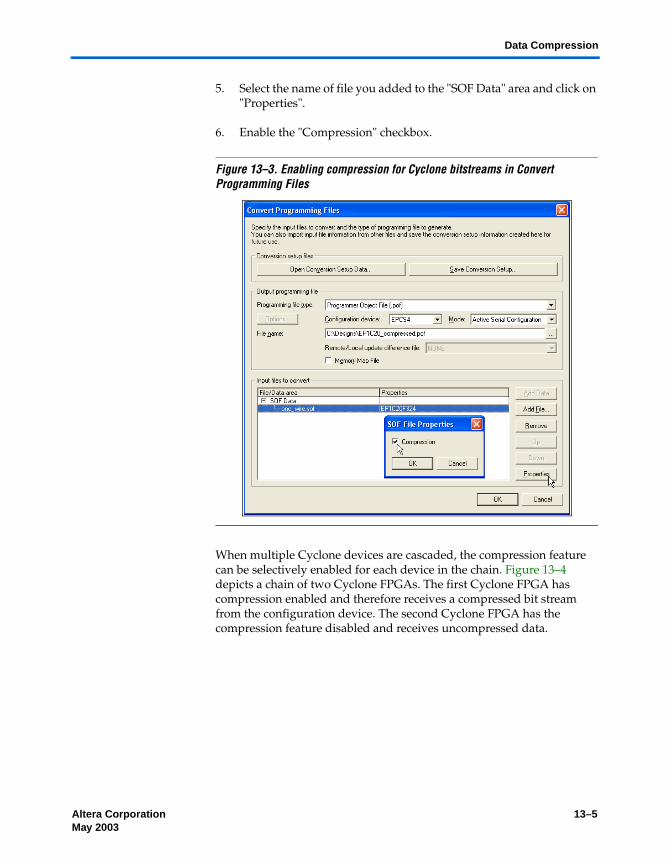
Altera Corporation 13–5May 2003 Preliminary
Data Compression
5. Select the name of file you added to the "SOF Data" area and click on "Properties".
6. Enable the "Compression" checkbox.
Figure 13–3. Enabling compression for Cyclone bitstreams in Convert Programming Files
When multiple Cyclone devices are cascaded, the compression feature can be selectively enabled for each device in the chain. Figure 13–4 depicts a chain of two Cyclone FPGAs. The first Cyclone FPGA has compression enabled and therefore receives a compressed bit stream from the configuration device. The second Cyclone FPGA has the compression feature disabled and receives uncompressed data.
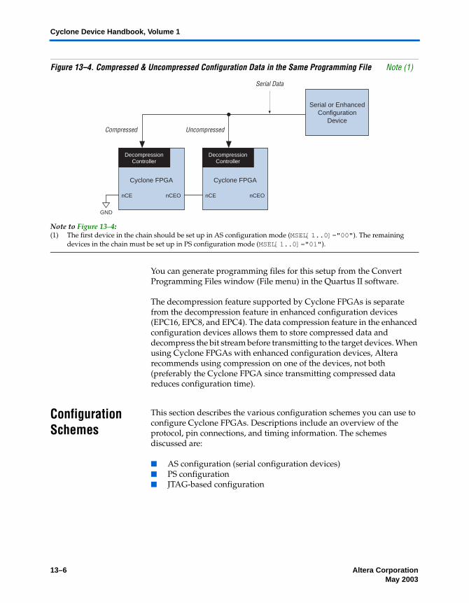
13–6 Altera CorporationPreliminary May 2003
Cyclone Device Handbook, Volume 1
Figure 13–4. Compressed & Uncompressed Configuration Data in the Same Programming File Note (1)
Note to Figure 13–4:(1) The first device in the chain should be set up in AS configuration mode (MSEL[1..0]="00"). The remaining
devices in the chain must be set up in PS configuration mode (MSEL[1..0]="01").
You can generate programming files for this setup from the Convert Programming Files window (File menu) in the Quartus II software.
The decompression feature supported by Cyclone FPGAs is separate from the decompression feature in enhanced configuration devices (EPC16, EPC8, and EPC4). The data compression feature in the enhanced configuration devices allows them to store compressed data and decompress the bit stream before transmitting to the target devices. When using Cyclone FPGAs with enhanced configuration devices, Altera recommends using compression on one of the devices, not both (preferably the Cyclone FPGA since transmitting compressed data reduces configuration time).
Configuration Schemes
This section describes the various configuration schemes you can use to configure Cyclone FPGAs. Descriptions include an overview of the protocol, pin connections, and timing information. The schemes discussed are:
AS configuration (serial configuration devices) PS configuration JTAG-based configuration
nCE
GND
nCEO
DecompressionController
Cyclone FPGA
nCE nCEO
DecompressionController
Cyclone FPGA
Serial or EnhancedConfiguration
Device
Serial Data
Compressed Uncompressed

Altera Corporation 13–7May 2003 Preliminary
Configuration Schemes
Active Serial Configuration (Serial Configuration Devices)
In the AS configuration scheme, Cyclone FPGAs are configured using the new serial configuration devices. These configuration devices are low cost devices with non-volatile memory that feature a simple four-pin interface and a small form factor. These features make serial configuration devices an ideal solution for configuring the low-cost Cyclone FPGAs.
f For more information on serial configuration devices, see Chapter 14, Serial Configuration Devices (EPCS1 & EPCS4) Data Sheet.
Serial configuration devices provide a serial interface to access configuration data. During device configuration, Cyclone FPGAs read configuration data via the serial interface, decompress data if necessary, and program their SRAM cells. This scheme is referred to as an AS configuration scheme because the FPGA controls the configuration interface. This scheme is in contrast to the PS configuration scheme where the configuration device controls the interface.
Serial configuration devices have a four-pin interface: serial clock input (DCLK), serial data output (DATA), AS data input (ASDI), and an active-low chip select (nCS). This four-pin interface connects to Cyclone FPGA pins, as shown in Figure 13–5.

13–8 Altera CorporationPreliminary May 2003
Cyclone Device Handbook, Volume 1
Figure 13–5. AS Configuration of a Single Cyclone FPGA
Notes to Figure 13–5: (1) Power up the ByteBlaster II Vcc with a 3.3-V supply.(2) The nCEO pin is left unconnected.(3) Cyclone FPGAs use the ASDO to ASDI path to control the configuration device.
Connecting the MSEL[1..0] pins to 00 selects the AS configuration scheme. The Cyclone chip enable signal, nCE, must also be connected to ground for successful configuration.
During system power up, both the Cyclone FPGA and serial configuration device enter a power-on reset (POR) period. As soon as the Cyclone FPGA enters POR, it drives nSTATUS low to indicate it is busy and drives CONF_DONE low to indicate that it has not been configured. After POR, which typically lasts 100 ms, the Cyclone FPGA releases nSTATUS and enters configuration mode when this signal is pulled high by the external 10-kΩ resistor.
The serial clock (DCLK) generated by the Cyclone FPGA controls the entire configuration cycle (see Figure 13–1 on page 13–2) and this clock line provides the timing for the serial interface. Cyclone FPGAs use an internal oscillator to generate DCLK. Typical DCLK frequency during AS configuration is 15 MHz.
The serial configuration device latches input/control signals on the rising edge of DCLK and drives out configuration data on the falling edge. Cyclone FPGAs drive out control signals on the falling edge of DCLK and latch configuration data on the rising edge of DCLK.
DATA
DCLK
nCS
ASDI
DATA0
DCLK
nCSO
ASDO
Serial ConfigurationDevice Cyclone FPGA
10 kΩ10 kΩ
VCC
10 kΩ
VCC VCC
GND
nCEO
nCE
nSTATUS
nCONFIGCONF_DONE
(3)
MSEL1
MSEL0
GND
N.C. (2)
(1) (1) (1)

Altera Corporation 13–9May 2003 Preliminary
Configuration Schemes
In configuration mode, the Cyclone FPGA enables the serial configuration device by driving the nCSO output pin low that is connected to the chip select (nCS) pin of the configuration device. The Cyclone FPGA’s serial clock (DCLK) and serial data output (ASDO) pins are used to read configuration data. The configuration device provides data on its serial data output (DATA) pin that is connected to the DATA0 input on Cyclone FPGAs.
After all configuration bits are received by the Cyclone FPGA, it releases the open-drain CONF_DONE pin allowing the external 10-kΩ resistor to pull this signal to a high level. Initialization begins only after the CONF_DONE line reaches a high level. Initialization completes within 136 clock cycles and the device enters user mode.
You can select the clock used for initialization by using the User Supplied Start-Up Clock option in the Quartus II software. The Quartus II software uses the 10-MHz internal oscillator by default to initialize the Cyclone FPGA. When you enable the User Supplied Start-Up Clock option, the software uses the CLKUSR pin as the initialization clock.
If an error occurs during configuration, the Cyclone FPGA asserts the nSTATUS signal low indicating a data frame error, and the CONF_DONE signal will stay low. With the Auto-Restart Configuration on Frame Error option enabled in the Quartus II software, the Cyclone FPGA resets the configuration device by pulsing nCSO, releases nSTATUS after a reset time-out period (about 30 micro-seconds), and retries configuration. After successful configuration, the CONF_DONE signal is tri-stated by the target device and then pulled high by the pull-up resistor.
All AS configuration pins, DATA0, DCLK, nCSO, and ASDO, have weak internal pull-up resistors. These pull-up resistors are always active.
Configuring Multiple Devices (Cascading)
You can configure multiple Cyclone FPGAs using a single serial configuration device. You can cascade multiple Cyclone FPGAs using the chip-enable (nCE) and chip-enable-out (nCEO) pins. The first device in the chain must have its nCE pin connected to ground. You must connect its nCEO chip-enable-out pin to the chip-enable (nCE) pin of the next device in the chain. When the first device captures all of its configuration data from the bit stream, it drives the nCEO pin low enabling the next device in the chain. You must leave the nCEO pin of the last device unconnected.
This first Cyclone FPGA in the chain is the configuration master and controls configuration of the entire chain. You must connect its MSEL pins to select the AS configuration scheme. The remaining Cyclone FPGAs are

13–10 Altera CorporationPreliminary May 2003
Cyclone Device Handbook, Volume 1
configuration slaves and you must connect their MSEL pins to select the PS configuration scheme. Figure 13–6 shows the pin connections for this setup.
Figure 13–6. Configuring Multiple Devices Using a Serial Configuration Device (AS)
Notes to Figure 13–6: (1) Power up the ByteBlaster II Vcc with a 3.3-V supply.(2) The nCEO pin is left unconnected.(3) Connect MSEL0 to the Vcc supply voltage of the I/O Bank it resides in.
As shown in Figure 13–6, the nSTATUS and CONF_DONE pins on all target FPGAs are connected together with external pull-up resistors. These pins are open-drain bidirectional pins on the FPGAs. When the first device asserts nCEO (after receiving all of its configuration data), it releases its CONF_DONE pin. But the subsequent devices in the chain keep this shared CONF_DONE line low until they have received their configuration data. When all target FPGAs in the chain have received their configuration data and have released CONF_DONE, the pull-up resistor drives a high level on this line and all devices simultaneously enter initialization mode. If an error occurs at any point during configuration, the nSTATUS line is driven by the failing FPGA. If you enable the Auto Restart Configuration on Frame Error option, reconfiguration of the entire chain begins.
DATA
DCLK
nCS
ASDI
DATA0
DCLK
nCSO
ASDO
Serial ConfigurationDevice Cyclone FPGA
10 kΩ10 kΩ
VCC VCC
GND
nCEOnCE
nSTATUSCONF_DONE
DATA0
DCLK
Cyclone FPGA
nCEO
nCE
nSTATUSCONF_DONE
SlaveMaster
10 kΩ
VCC
nCONFIG nCONFIG
MSEL1
MSEL0
GND
VCC
N.C. (2)
MSEL1
MSEL0
GND
(1) (1) (1)
(3)

Altera Corporation 13–11May 2003 Preliminary
Configuration Schemes
Furthermore, while you can cascade Cyclone FPGAs, serial configuration devices cannot be cascaded or chained together. If the configuration bit stream size exceeds the capacity of a serial configuration device, you must select a larger configuration device and/or enable the compression feature. While configuring multiple devices, the size of the bit stream is the sum of the individual devices’ configuration bit streams.
Programming Serial Configuration Devices
Serial configuration devices are non-volatile, flash-memory-based devices. You can program these devices in-system using the ByteBlasterTM II download cable. Alternatively, you can program them using the Altera Programming Unit (APU) or supported third-party programmers.
You can perform in-system programming of serial configuration devices via the AS programming interface. During in-system programming, the download cable disables FPGA access to the AS interface by driving the chip-enable nCE pin high. Cyclone FPGAs are also held in reset by a low level on nCONFIG. After programming is complete, the download cable releases nCE and nCONFIG, allowing the pull-down and pull-up resistor to drive GND and VCC, respectively. Figure 13–7 shows the download cable connections to the serial configuration device.
f For more information on the ByteBlaster II cable, see the ByteBlaster II Download Cable Data Sheet.
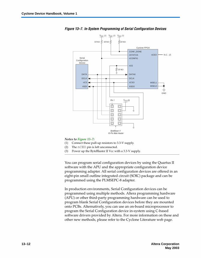
13–12 Altera CorporationPreliminary May 2003
Cyclone Device Handbook, Volume 1
Figure 13–7. In-System Programming of Serial Configuration Devices
Notes to Figure 13–7:(1) Connect these pull-up resistors to 3.3-V supply.(2) The nCEO pin is left unconnected.(3) Power up the ByteBlaster II Vcc with a 3.3-V supply.
You can program serial configuration devices by using the Quartus II software with the APU and the appropriate configuration device programming adapter. All serial configuration devices are offered in an eight-pin small outline integrated circuit (SOIC) package and can be programmed using the PLMSEPC-8 adapter.
In production environments, Serial Configuration devices can be programmed using multiple methods. Altera programming hardware (APU) or other third-party programming hardware can be used to program blank Serial Configuration devices before they are mounted onto PCBs. Alternatively, you can use an on-board microprocessor to program the Serial Configuration device in-system using C-based software drivers provided by Altera. For more information on these and other new methods, please refer to the Cyclone Literature web page.
DATA
DCLK
nCS
ASDI
DATA0
DCLK
nCSO
nCE
nCONFIG
nSTATUS nCEO
CONF_DONE
ASDO
VCC VCC VCC
VCC
10 kΩ 10 kΩ 10 kΩ
10 kΩ
Cyclone FPGA
SerialConfiguration
Device
Pin 1
MSEL1
MSEL0
GND
ByteBlaser II 10-Pin Male Header
(2)N.C.
(1) (1) (1)
(3)

Altera Corporation 13–13May 2003 Preliminary
Configuration Schemes
Passive Serial Configuration
Cyclone FPGAs also feature the PS configuration scheme supported by all Altera FPGAs. In the PS scheme, an external host (configuration device, embedded processor, or host PC) controls configuration. Configuration data is clocked into the target Cyclone FPGAs via the DATA0 pin at each rising edge of DCLK. The configuration waveforms for this scheme are shown in Figure 13–8.
Figure 13–8. PS Configuration Cycle Waveform
Notes to Figure 13–8:(1) During initial power up and configuration, CONF_DONE is low. After configuration, CONF_DONE goes high to
indicate successful configuration. If the device is reconfigured, CONF_DONE goes low after nCONFIG is driven low.(2) User I/O pins are tri-stated during configuration. Cyclone FPGAs also have a weak pull-up resistor on I/O pins
during configuration. After initialization, the user I/O pins perform the function assigned in the user’s design.(3) When used, the optional INIT_DONE signal is high when nCONFIG is low before configuration and during the first
136 clock cycles of configuration.(4) In user mode, DCLK should be driven high or low when using the PS configuration scheme. When using the AS
configuration scheme, DCLK is a Cyclone output pin and should not be driven externally.(5) In user mode, DATA0 should be driven high or low.
PS Configuration using Configuration Device
In the PS configuration device scheme, nCONFIG is usually tied to VCC (when using EPC16, EPC8, EPC4, or EPC2 devices, you can connect nCONFIG to nINIT_CONF). Upon device power-up, the target Cyclone FPGA senses the low-to-high transition on nCONFIG and initiates configuration. The target device then drives the open-drain CONF_DONE pin low, which in-turn drives the configuration device’s nCS pin low. When exiting POR, both the target and configuration device release the open-drain nSTATUS pin (typically Cyclone POR lasts 100 ms).
Before configuration begins, the configuration device goes through a POR delay of up to 100 ms (maximum) to allow the power supply to stabilize. You must power the Cyclone FPGA before or during the POR
High-Z
nCONFIG
nSTATUS
CONF_DONE (1)
DCLK
DATA
User I/O Pins (2)
INIT_DONE (3)
MODE
High-Z D0 D1 D2 D3
D(N – 1)
DN
Configuration Initialization User
High-Z User I/O
Configuration
(4)
(5)

13–14 Altera CorporationPreliminary May 2003
Cyclone Device Handbook, Volume 1
time of the enhanced configuration device. During POR, the configuration device drives its OE pin low. This low signal delays configuration because the OE pin is connected to the target device’s nSTATUS pin. When the target and configuration devices complete POR, they both release the nSTATUS to OE line, which is then pulled high by a pull-up resistor.
When configuring multiple devices, configuration does not begin until all devices release their OE or nSTATUS pins. When all devices are ready, the configuration device clocks out DATA and DCLK to the target devices using an internal oscillator.
After successful configuration, the Cyclone FPGA starts initialization using the 10-MHz internal oscillator as the reference clock. The CONF_DONE pin is released by the target device and then pulled high by a pull-up resistor. When initialization is complete, the target Cyclone FPGA enters user mode.
If an error occurs during configuration, the target device drives its nSTATUS pin low, resetting itself internally and resetting the configuration device. If you turn on the Auto-Restart Configuration on Frame Error option, the device reconfigures automatically if an error occurs. To set this option, select Compiler Settings (Processing menu), and click on the Chips & Devices tab. Select Device & Pin Options, and click on the Configuration tab.
If the Auto-Restart Configuration on Frame Error option is turned off, the external system (configuration device or microprocessor) must monitor nSTATUS for errors and then pulse nCONFIG low to restart configuration. The external system can pulse nCONFIG if it is under system control rather than tied to VCC. When configuration is complete, the target device releases CONF_DONE, which disables the configuration device by driving nCS high. The configuration device drives DCLK low before and after configuration.
In addition, if the configuration device sends all of its data and then detects that CONF_DONE has not gone high, it recognizes that the target device has not configured successfully. (For CONF_DONE to reach a high state, enhanced configuration devices wait for 64 DCLK cycles after the last configuration bit. EPC2 devices wait for 16 DCLK cycles.) In this case, the configuration device pulses its OE pin low for a few microseconds, driving the target device’s nSTATUS pin low. If the Auto-Restart Configuration on Frame Error option is set in the Quartus II software, the target device resets and then releases its nSTATUS pin after a reset time-out period. When nSTATUS returns high, the configuration device reconfigures the target device.

Altera Corporation 13–15May 2003 Preliminary
Configuration Schemes
You should not pull CONF_DONE low to delay initialization. Instead, use the Quartus II software’s User-Supplied Start-Up Clock option to synchronize the initialization of multiple devices that are not in the same configuration chain. Devices in the same configuration chain initialize together since their CONF_DONE pins are tied together. For more information on this option, see “Device Options” on page 13–41.
CONF_DONE goes high during the first few clock cycles of initialization. Hence when using the CLKUSR feature you would not see the CONF_DONE signal high until you start clocking CLKUSR. However, the device does retain configuration data and waits for these initialization clocks to release CONF_DONE and go into user mode.
1 When using internal pull-up resistors on configuration devices, power the supply voltage on the Cyclone FPGA I/O pins (VCCIO) to 3.3-V. EPC2, EPC4, EPC8, and EPC16 devices support 3.3-V operation but not 2.5-V operation. Therefore, you must set the VCCIO voltages for the banks where programming pins reside to 3.3 V.
Figure 13–9 shows how to configure one Cyclone FPGA with one configuration device.
Figure 13–9. Single Device Configuration Circuit
Notes to Figure 13–9:(1) The pull-up resistor should be connected to the same supply voltage as the
configuration device. This pull-up resistor is 10 kΩ. The EPC16, EPC8, EPC4, and EPC2 devices’ OE and nCS pins have internal, user-configurable pull-up resistors. If you use internal pull-up resistors, do not use external pull-up resistors on these pins.
(2) The nINIT_CONF pin is available on EPC16, EPC8, EPC4, and EPC2 devices and has an internal pull-up resistor that is always active. If nINIT_CONF is not used, nCONFIG must be pulled to VCC through a resistor.
(3) The nCEO pin is left unconnected for the last device in the chain.(4) Connect MSEL0 to the Vcc supply voltageof I/O Bank it resides in.
Cyclone FPGADCLKDATAOEnCSnINIT_CONF (2)
MSEL0MSEL1
DCLKDATA0
nSTATUSCONF_DONE
nCONFIG
VCC VCC
GND
(1) (1)
nCE
nCEO N.C. (3)
ConfigurationDevice10 kΩ 10 kΩ10 kΩ
VCC
VCC (1)
GND
(4)

13–16 Altera CorporationPreliminary May 2003
Cyclone Device Handbook, Volume 1
Configuring Multiple Cyclone FPGAs
You can use a single configuration device to configure multiple Cyclone FPGAs. In this setup, the nCEO pin of the first device is connected to the nCE pin of the second device in the chain. If there are additional devices, connect the nCE pin of the next device to the nCEO pin of the previous device. You should leave the nCEO pin on the last device in the chain unconnected. To configure properly, all of the target device CONF_DONE and nSTATUS pins must be tied together. Figure 13–10 shows an example of configuring multiple Cyclone FPGAs using a single configuration device.
Figure 13–10. Configuring Multiple Cyclone FPGAs with a Single Configuration Device
Notes to Figure 13–10:(1) The pull-up resistor should be connected to the same supply voltage as the configuration device. The EPC16, EPC8,
EPC4, and EPC2 devices’ OE and nCS pins have internal, user-configurable pull-up resistors. If you use internal pull-up resistors, do not use external pull-up resistors on these pins.
(2) EPC16, EPC8, and EPC4 configuration devices cannot be cascaded.(3) The nCEO pin is left unconnected for the last device in the chain.(4) The nINIT_CONF pin is available on EPC16, EPC8, EPC4, and EPC2 devices. If nINIT_CONF is not used, nCONFIG
must be pulled to VCC through a resistor.(5) The nINIT_CONF pin has an internal pull-up resistor that is always active in EPC16, EPC8, EPC4, and EPC2 devices.
These devices do not need an external pull-up resistor on the nINIT_CONF pin.(6) Connect MSEL0 to the Vcc supply voltageof I/O Bank it resides in.
When performing multi-device PS configuration, you must generate the configuration device programming file (.sof) from each project. Then you must combine multiple .sof files using the Quartus II software through the Convert Programming Files dialog box.
ConfigurationDevice (2)
DCLKDATAOEnCSnINIT_CONF (4), (5)
DCLKDATA0
nSTATUSCONF_DONE
nCONFIG
VCC VCC
GND
nCE
VCC
DCLKDATA0
nSTATUSCONF_DONE
nCONFIGGND
nCE
MSEL1
nCEO
nCASC
(1) (1)
(1)
nCEO (3)N.C.
Cyclone FPGA 2 Cyclone FPGA 1
MSEL0
VCC
GND
MSEL1MSEL0
VCC
10 kΩ 10 kΩ 10 kΩ
(6)(6)

Altera Corporation 13–17May 2003 Preliminary
Configuration Schemes
f For more information on how to create Programmer Object Files (.pof) for enhanced configuration devices, see Application Note 218: Using Enhanced Configuration Devices. For a description of the various configuration and programming files, see “Device Configuration Files” on page 13–47.
After the first Cyclone FPGA completes configuration during multi-device configuration, its nCEO pin activates the second device’s nCE pin, prompting the second device to begin configuration. Because all device CONF_DONE pins are tied together, all devices initialize and enter user mode at the same time.
In addition, all nSTATUS pins are tied together; therefore, if any device (including the configuration device) detects an error, configuration stops for the entire chain. Also, if the configuration device does not detect CONF_DONE going high at the end of configuration, it resets the chain by pulsing its OE pin low for a few microseconds. For CONF_DONE to reach a high state, enhanced configuration devices wait for 64 DCLK cycles after the last configuration bit. EPC2 devices wait for 16 DCLK cycles.
If the Auto-Restart Configuration on Frame Error option is turned on in the Quartus II software, the Cyclone FPGA releases its nSTATUS pins after a reset time-out period (about 30 micro-seconds). When the nSTATUS pins are released and pulled high, the configuration device reconfigures the chain. If the Auto-Restart Configuration on Frame Error option is not turned on, the devices drive nSTATUS low until they are reset with a low pulse on nCONFIG.
You can also cascade several EPC2 configuration devices to configure multiple Cyclone FPGAs. When all data from the first configuration device is sent, it drives nCASC low, which in turn drives nCS on the subsequent EPC2 device. Because a configuration device requires less than one clock cycle to activate a subsequent configuration device, the data stream is uninterrupted. You cannot cascade EPC16, EPC8, and EPC4 configuration devices.
Programming Configuration Devices
Enhanced configuration devices (EPC4, EPC8, and EPC16 devices) and EPC2 devices support in-system programming via JTAG. You can program these configuration devices using the Quartus II software and a download cable (e.g., ByteBlaster II, MasterBlasterTM, or ByteBlasterMVTM cables).

13–18 Altera CorporationPreliminary May 2003
Cyclone Device Handbook, Volume 1
You can also program configuration devices using the Quartus II software, the APU, and the appropriate configuration device programming adapter. Table 13–4 shows which programming adapter to use with each configuration device.
PS Configuration Using a Download Cable
Using a download cable in PS configuration, an intelligent host (e.g., your PC) transfers data from a storage device (e.g., your hard drive) to the Cyclone FPGA through a ByteBlaster II, MasterBlaster, or ByteBlasterMV cable. To initiate configuration in this scheme, the download cable generates a low-to-high transition on the nCONFIG pin. The programming hardware then sends the configuration data one bit at a time on the device’s DATA0 pin. The data is clocked into the target device using DCLK until the CONF_DONE goes high.
When using programming hardware for the Cyclone FPGA, turning on the Auto-Restart Configuration on Frame Error option does not affect the configuration cycle because the Quartus II software must restart configuration when an error occurs. Figure 13–11 shows the PS configuration setup for the Cyclone FPGA using a ByteBlaster II, MasterBlaster, or ByteBlasterMV cable.
Table 13–4. Programming Adapters
Device Package Adapter
EPC16 88-pin Ultra FineLine BGA®
100-pin PQFPPLMUEPC-88PLMQEPC-100
EPC8 100-pin PQFP PLMQEPC-100
EPC4 100-pin PQFP PLMQEPC-100
EPC2 20-pin J-Lead32-pin TQFP
PLMJ1213PLMT1213
EPC1 8-pin DIP20-pin J-Lead
PLMJ1213PLMJ1213

Altera Corporation 13–19May 2003 Preliminary
Configuration Schemes
Figure 13–11. PS Configuration Circuit with ByteBlaster II, MasterBlaster, or ByteBlasterMV Cable
Notes to Figure 13–11:(1) You should connect the pull-up resistor to the same supply voltage as the MasterBlaster (VIO pin) or ByteBlasterMV
cable.(2) Power supply voltage: VCC = 3.3-V for the ByteBlaster II, MasterBlaster, and ByteBlasterMV cable.(3) Pin 6 of the header is a VIO reference voltage for the MasterBlaster output driver. VIO should match the device’s
VCCIO. This pin is a no-connect pin for the ByteBlasterMV header.(4) The pull-up resistors on DATA0 and DCLK are only needed if the download cable is the only configuration scheme
used on your board. This is to ensure that DATA0 and DCLK are not left floating after configuration. For example, if you are also using a configuration device, the pull-up resistors on DATA0 and DCLK are not needed.
(5) Connect MSEL0 to the Vcc supply voltageof I/O Bank it resides in.
You can use the download cable to configure multiple Cyclone FPGAs by connecting each device’s nCEO pin to the subsequent device’s nCE pin. All other configuration pins are connected to each device in the chain.
Because all CONF_DONE pins are tied together, all devices in the chain initialize and enter user mode at the same time. In addition, because the nSTATUS pins are tied together, the entire chain halts configuration if any device detects an error. In this situation, the Quartus II software must restart configuration; the Auto-Restart Configuration on Frame Error option does not affect the configuration cycle. Figure 13–12 shows how to configure multiple Cyclone FPGAs with a ByteBlaster II, MasterBlaster, or ByteBlasterMV cable.
ByteBlaster II, MasterBlaster, or ByteBlasterMV
10-Pin Male Header
VCC (1)VCC (1)
VCC (2)
VCC (1)
Cyclone Device
DCLK
nCONFIG
CONF_DONE
ShieldGND
MSEL1MSEL0
10 kΩ10 kΩ 10 kΩ
nSTATUS
DATA0 Pin 1
nCE
GND
GNDVIO (3)
VCC
VCC (1)
10 kΩ(4)
VCC (1)
10 kΩ(4)
(5)
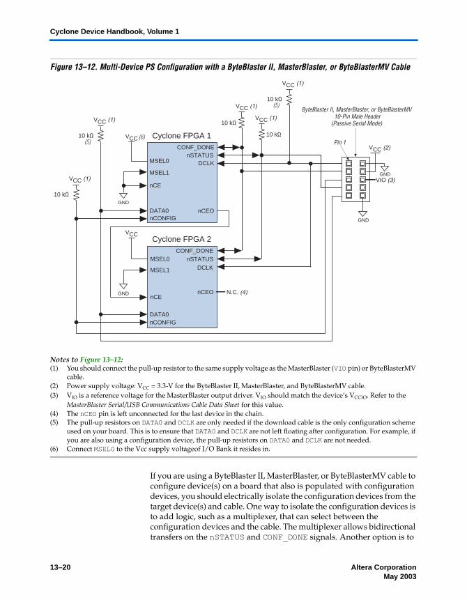
13–20 Altera CorporationPreliminary May 2003
Cyclone Device Handbook, Volume 1
Figure 13–12. Multi-Device PS Configuration with a ByteBlaster II, MasterBlaster, or ByteBlasterMV Cable
Notes to Figure 13–12:(1) You should connect the pull-up resistor to the same supply voltage as the MasterBlaster (VIO pin) or ByteBlasterMV
cable.(2) Power supply voltage: VCC = 3.3-V for the ByteBlaster II, MasterBlaster, and ByteBlasterMV cable.(3) VIO is a reference voltage for the MasterBlaster output driver. VIO should match the device’s VCCIO. Refer to the
MasterBlaster Serial/USB Communications Cable Data Sheet for this value.(4) The nCEO pin is left unconnected for the last device in the chain.(5) The pull-up resistors on DATA0 and DCLK are only needed if the download cable is the only configuration scheme
used on your board. This is to ensure that DATA0 and DCLK are not left floating after configuration. For example, if you are also using a configuration device, the pull-up resistors on DATA0 and DCLK are not needed.
(6) Connect MSEL0 to the Vcc supply voltageof I/O Bank it resides in.
If you are using a ByteBlaster II, MasterBlaster, or ByteBlasterMV cable to configure device(s) on a board that also is populated with configuration devices, you should electrically isolate the configuration devices from the target device(s) and cable. One way to isolate the configuration devices is to add logic, such as a multiplexer, that can select between the configuration devices and the cable. The multiplexer allows bidirectional transfers on the nSTATUS and CONF_DONE signals. Another option is to
Cyclone FPGA 1
Cyclone FPGA 2
MSEL0
nCE
nCONFIG
CONF_DONE
DCLK
nCEnCEO
nCONFIG
CONF_DONE
DCLK
nCEO
GND
(Passive Serial Mode)
VCC (2)
VCC (1)GND
VCC (1)
VCC (1)
nSTATUS
nSTATUS
DATA0
DATA0
MSEL1
MSEL0
MSEL1
10 kΩ
10 kΩ
10 kΩ
Pin 1
ByteBlaster II, MasterBlaster, or ByteBlasterMV 10-Pin Male Header
N.C. (4)
VIO (3)
GND
VCC
GND
VCC
VCC (1)
10 kΩ(5)
(6)
VCC (1)
10 kΩ(5)

Altera Corporation 13–21May 2003 Preliminary
Configuration Schemes
add switches to the five common signals (CONF_DONE, nSTATUS, DCLK, nCONFIG, and DATA0) between the cable and the configuration devices. The last option is to remove the configuration devices from the board when configuring with the cable. Figure 13–13 shows a combination of a configuration device and a ByteBlaster II, MasterBlaster, or ByteBlasterMV cable to configure a Cyclone FPGA.
Figure 13–13. Configuring with a Combined PS & Configuration Device Scheme
Notes to Figure 13–13:(1) You should connect the pull-up resistor to the same supply voltage as the configuration device.(2) Power supply voltage: VCC = 3.3-V for the ByteBlaster II, MasterBlaster, and ByteBlasterMV cable.(3) Pin 6 of the header is a VIO reference voltage for the MasterBlaster output driver. VIO should match the target
device’s VCCIO. This is a no-connect pin for the ByteBlasterMV header.(4) The nCEO pin is left unconnected.(5) You should not attempt configuration with a ByteBlaster II, MasterBlaster, or ByteBlasterMV cable while a
configuration device is connected to a Cyclone FPGA. Instead, you should either remove the configuration device from its socket when using the download cable or place a switch on the five common signals between the download cable and the configuration device. Remove the ByteBlaster II, MasterBlaster, or ByteBlasterMV cable when configuring with a configuration device.
(6) If nINIT_CONF is not used, nCONFIG must be pulled to VCC either directly or through a resistor.(7) The pull-up resistors on DATA0 and DCLK are only needed if the download cable is the only configuration scheme
used on your board. This is to ensure that DATA0 and DCLK are not left floating after configuration. For example, if you are also using a configuration device, the pull-up resistors on DATA0 and DCLK are not needed.
(8) Connect MSEL0 to the Vcc supply voltageof I/O Bank it resides in.
Cyclone FPGA
MSEL0
nCE
nCONFIG
CONF_DONE
DCLK
nCEO
GND
ByteBlaster II, MasterBlaster, or ByteBlasterMV10-Pin Male Header
(Passive Serial Mode)
VCC (2)
VCC
VCC (1)
VCC (1)
nSTATUS
DATA0
MSEL1
10 kΩ
10 kΩ
10 kΩPin 1
DCLKDATAOEnCS
nINIT_CONF (6)
Configuration Device
(5)
(5) (5) (5)
(5)
GNDVIO (3)
N.C. (4)
(1)
GND
VCC
VCC
10 kΩ
(1)
(7)
(8)VCC
10 kΩ
(1)
(7)

13–22 Altera CorporationPreliminary May 2003
Cyclone Device Handbook, Volume 1
f For more information on how to use the ByteBlaster II, MasterBlaster, or ByteBlasterMV cables, see the following documents:
ByteBlaster II Parallel Port Download Cable Data Sheet MasterBlaster Serial/USB Communications Cable Data Sheet ByteBlasterMV Parallel Port Download Cable Data Sheet
PS Configuration from a Microprocessor
In PS configuration with a microprocessor, a microprocessor transfers data from a storage device to the target Cyclone FPGA. To initiate configuration in this scheme, the microprocessor must generate a low-to-high transition on the nCONFIG pin and the target device must release nSTATUS. The microprocessor then places the configuration data one bit at a time on the DATA0 pin of the Cyclone FPGA. The least significant bit (LSB) of each data byte must be presented first. Data is clocked continuously into the target device using DCLK until the CONF_DONE signal goes high.
The Cyclone FPGA starts initialization using the internal oscillator after all configuration data is transferred. The device’s CONF_DONE pin goes high to show successful configuration and the start of initialization. Driving DCLK to the device after configuration does not affect device operation.
Since the PS configuration scheme is a synchronous scheme, the configuration clock speed must be below the specified maximum frequency to ensure successful configuration. Maximum DCLK frequency supported by Cyclone FPGAs is 100 MHz (See Table 13–5 on page 13–24). No maximum DCLK period (i.e., minimum DCLK frequency) exists. You can pause configuration by halting DCLK for an indefinite amount of time.
If the target device detects an error during configuration, it drives its nSTATUS pin low to alert the microprocessor. The microprocessor can then pulse nCONFIG low to restart the configuration process. Alternatively, if the Auto-Restart Configuration on Frame Error option is turned on in the Quartus II software, the target device releases nSTATUS after a reset time-out period. After nSTATUS is released, the microprocessor can reconfigure the target device without needing to pulse nCONFIG low.
The microprocessor can also monitor the CONF_DONE and INIT_DONE pins to ensure successful configuration and initialization. If the microprocessor sends all data but CONF_DONE and INIT_DONE has not gone high, it must reconfigure the target device. CONF_DONE should go

Altera Corporation 13–23May 2003 Preliminary
Configuration Schemes
high within 1 ms, and INIT_DONE should go high within 15 ms. Figure 13–14 shows the circuit for PS configuration with a microprocessor.
Figure 13–14. PS Configuration Circuit with a Microprocessor
Note to Figure 13–14:(1) The nCEO pin is left unconnected.(2) Connect MSEL0 to the Vcc supply voltageof I/O Bank it resides in.
Configuring Cyclone FPGAs with the MicroBlaster Software
The MicroBlasterTM software driver allows you to configure Altera FPGAs, including Cyclone FPGAs, through the ByteBlaster II or ByteBlasterMV cable in PS mode. The MicroBlaster software driver supports a Raw Binary File (.rbf) programming input file and is targeted for embedded PS configuration. The source code is developed for the Windows NT operating system, although you can customize it to run on other operating systems. For more information on the MicroBlaster software driver, see the Configuring the MicroBlaster Passive Serial Software Driver White Paper and source files on the Altera web site at www.altera.com.
Passive Serial Timing
For successful configuration using the PS scheme, several timing parameters such as setup, hold, and maximum clock frequency must be satisfied. The enhanced configuration and EPC2 devices are designed to meet these interface timing specifications. If you use a microprocessor or another intelligent host to control the PS interface, ensure that you meet these timing requirements.
Microprocessor
CONF_DONE
nSTATUS
nCE
DATA0
nCONFIG
Cyclone Device
Memory
ADDR DATA0
GND
MSEL1
VCCVCC
10 kΩ 10 kΩ
GND
DCLK
nCEO N.C. (1)
MSEL0
VCC (2)

13–24 Altera CorporationPreliminary May 2003
Cyclone Device Handbook, Volume 1
Figure 13–15 shows the PS timing waveform for Cyclone FPGAs.
Figure 13–15. PS Timing Waveform for Cyclone FPGAs
Notes to Figure 13–15:(1) Upon power-up, the Cyclone FPGA holds nSTATUS low for about 100 ms.(2) Upon power-up and before configuration, CONF_DONE is low.(3) In user mode, DCLK should be driven high or low when using the PS configuration scheme. When using the AS
configuration scheme, DCLK is a Cyclone output pin and should not be driven externally.(4) DATA should not be left floating after configuration. It should be driven high or low, whichever is more convenient.
Table 13–5 contains the PS timing information for Cyclone FPGAs.
nCONFIG
nSTATUS (1)
CONF_DONE (2)
DCLK (3)
DATA
User I/O
INIT_DONE
Bit 0 Bit 1 Bit 2 Bit 3 Bit n
tCD2UM
tCF2ST1
tCF2CD
tCFG
tCH tCL
tDH
tDSU
tCF2CK
tSTATUS
tCLKtCF2ST0
tST2CK
High-Z User Mode
(4)
Table 13–5. PS Timing Parameters for Cyclone Devices Note (1) (Part 1 of 2)
Symbol Parameter Min Max Units
tCF2CD nCONFIG low to CONF_DONE low 800 ns
tCF2ST0 nCONFIG low to nSTATUS low 800 ns
tCF2ST1 nCONFIG high to nSTATUS high 40 (4) µs
tCFG nCONFIG low pulse width (2) 40 µs
tSTATUS nSTATUS low pulse width 10 40 (4) µs
tCF2CK nCONFIG high to first rising edge on DCLK 40 µs
tST2CK nSTATUS high to first rising edge on DCLK 1 µs
tDSU Data setup time before rising edge on DCLK 7 ns
tDH Data hold time after rising edge on DCLK 0 ns
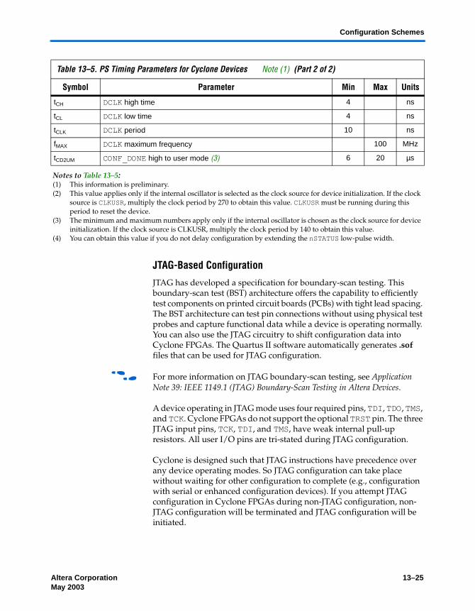
Altera Corporation 13–25May 2003 Preliminary
Configuration Schemes
JTAG-Based Configuration
JTAG has developed a specification for boundary-scan testing. This boundary-scan test (BST) architecture offers the capability to efficiently test components on printed circuit boards (PCBs) with tight lead spacing. The BST architecture can test pin connections without using physical test probes and capture functional data while a device is operating normally. You can also use the JTAG circuitry to shift configuration data into Cyclone FPGAs. The Quartus II software automatically generates .sof files that can be used for JTAG configuration.
f For more information on JTAG boundary-scan testing, see Application Note 39: IEEE 1149.1 (JTAG) Boundary-Scan Testing in Altera Devices.
A device operating in JTAG mode uses four required pins, TDI, TDO, TMS, and TCK. Cyclone FPGAs do not support the optional TRST pin. The three JTAG input pins, TCK, TDI, and TMS, have weak internal pull-up resistors. All user I/O pins are tri-stated during JTAG configuration.
Cyclone is designed such that JTAG instructions have precedence over any device operating modes. So JTAG configuration can take place without waiting for other configuration to complete (e.g., configuration with serial or enhanced configuration devices). If you attempt JTAG configuration in Cyclone FPGAs during non-JTAG configuration, non-JTAG configuration will be terminated and JTAG configuration will be initiated.
tCH DCLK high time 4 ns
tCL DCLK low time 4 ns
tCLK DCLK period 10 ns
fMAX DCLK maximum frequency 100 MHz
tCD2UM CONF_DONE high to user mode (3) 6 20 µs
Notes to Table 13–5:(1) This information is preliminary.(2) This value applies only if the internal oscillator is selected as the clock source for device initialization. If the clock
source is CLKUSR, multiply the clock period by 270 to obtain this value. CLKUSR must be running during this period to reset the device.
(3) The minimum and maximum numbers apply only if the internal oscillator is chosen as the clock source for device initialization. If the clock source is CLKUSR, multiply the clock period by 140 to obtain this value.
(4) You can obtain this value if you do not delay configuration by extending the nSTATUS low-pulse width.
Table 13–5. PS Timing Parameters for Cyclone Devices Note (1) (Part 2 of 2)
Symbol Parameter Min Max Units
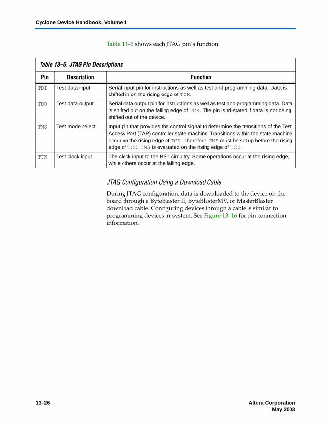
13–26 Altera CorporationPreliminary May 2003
Cyclone Device Handbook, Volume 1
Table 13–6 shows each JTAG pin’s function.
JTAG Configuration Using a Download Cable
During JTAG configuration, data is downloaded to the device on the board through a ByteBlaster II, ByteBlasterMV, or MasterBlaster download cable. Configuring devices through a cable is similar to programming devices in-system. See Figure 13–16 for pin connection information.
Table 13–6. JTAG Pin Descriptions
Pin Description Function
TDI Test data input Serial input pin for instructions as well as test and programming data. Data is shifted in on the rising edge of TCK.
TDO Test data output Serial data output pin for instructions as well as test and programming data. Data is shifted out on the falling edge of TCK. The pin is tri-stated if data is not being shifted out of the device.
TMS Test mode select Input pin that provides the control signal to determine the transitions of the Test Access Port (TAP) controller state machine. Transitions within the state machine occur on the rising edge of TCK. Therefore, TMS must be set up before the rising edge of TCK. TMS is evaluated on the rising edge of TCK.
TCK Test clock input The clock input to the BST circuitry. Some operations occur at the rising edge, while others occur at the falling edge.

Altera Corporation 13–27May 2003 Preliminary
Configuration Schemes
Figure 13–16. JTAG Configuration of Single Cyclone FPGA
Notes to Figure 13–16:(1) You should connect the pull-up resistor to the same supply voltage as the download cable.(2) You should connect the nCONFIG, MSEL0, and MSEL1 pins to support a non-JTAG configuration scheme. If you only
use JTAG configuration, connect nCONFIG to VCC, and MSEL0 and MSEL1 to ground. Pull DATA0 and DCLK to high or low.
(3) VIO is a reference voltage for the MasterBlaster output driver. VIO should match the device’s VCCIO. Refer to the MasterBlaster Serial/USB Communications Cable Data Sheet for this value.
To configure a single device in a JTAG chain, the programming software places all other devices in bypass mode. In bypass mode, devices pass programming data from the TDI pin to the TDO pin through a single bypass register without being affected internally. This scheme enables the programming software to program or verify the target device. Configuration data driven into the device appears on the TDO pin one clock cycle later.
Cyclone FPGAs have dedicated JTAG pins. Not only can you perform JTAG testing on Cyclone FPGAs before and after, but also during configuration. While other device families do not support JTAG testing during configuration, Cyclone FPGAs support the BYPASS, IDCODE, and SAMPLE instructions during configuration without interrupting configuration. All other JTAG instructions may only be issued by first interrupting configuration and reprogramming I/O pins using the CONFIG_IO instruction.
nCE
MSEL0MSEL1
nCONFIGCONF_DONE
VCC (1)
GND
VCC
GND
VCC
(2)(2)
(2)
10 kΩ
10 kΩ
nSTATUS ByteBlaster II, MasterBlaster, or ByteBlasterMV 10-Pin Male Header
(Top View)
TCKTDO
TMSTDI
GNDVIO (3)
Cyclone Device
DATA0DCLK
(2)(2)
Pin 1
VCC
10 kΩ
VCC
10 kΩ
10 kΩ
GND

13–28 Altera CorporationPreliminary May 2003
Cyclone Device Handbook, Volume 1
The CONFIG_IO instruction allows I/O buffers to be configured via the JTAG port, and when issued, interrupts configuration. This instruction allows you to perform board-level testing prior to configuring the Cyclone FPGA or waiting for a configuration device to complete configuration. Once configuration has been interrupted and JTAG testing is complete, the part must be reconfigured via JTAG (PULSE_CONFIG instruction) or by pulsing nCONFIG low.
The chip-wide reset and output enable pins on Cyclone FPGAs do not affect JTAG boundary-scan or programming operations. Toggling these pins does not affect JTAG operations (other than the usual boundary-scan operation).
When designing a board for JTAG configuration of Cyclone FPGAs, you should consider the regular configuration pins. Table 13–7 shows how you should connect these pins during JTAG configuration.
JTAG Configuration of Multiple Devices
When programming a JTAG device chain, one JTAG-compatible header, such as the ByteBlaster II header, is connected to several devices. The number of devices in the JTAG chain is limited only by the drive capacity of the download cable. However, when four or more devices are connected in a JTAG chain, Altera recommends buffering the TCK, TDI, and TMS pins with an on-board buffer.
Table 13–7. JTAG Termination of Unused Pins
Signal Description
nCE Drive all Cyclone devices in the chain low by connecting nCE to ground, pulling it down via a resistor, or driving it low by some control circuitry.
nSTATUS Pulled to VCC through a 10-kΩ resistor. When configuring multiple devices in the same JTAG chain, pull up each nSTATUS pin to VCC individually. (1)
CONF_DONE Pulled to VCC through a 10-kΩ resistor. When configuring multiple devices in the same JTAG chain, pull up each CONF_DONE pin to VCC individually. (1)
nCONFIG Driven high by connecting to VCC, pulling up through a resistor, or driving it high by some control circuitry.
MSEL0, MSEL1
Do not leave these pins floating. These pins support whichever non-JTAG configuration is used in production. If only JTAG configuration is used, you should tie these pins to ground.
DCLK Do not leave these pins floating. Drive low or high, whichever is more convenient.
DATA0 Do not leave these pins floating. Drive low or high, whichever is more convenient.
Note to Table 13–7:(1) nSTATUS going low in the middle of JTAG configuration indicates that an error has occurred; CONF_DONE going
high at the end of JTAG configuration indicates successful configuration.

Altera Corporation 13–29May 2003 Preliminary
Configuration Schemes
JTAG-chain device configuration is ideal when the system contains multiple devices, or when testing your system using JTAG BST circuitry. Figure 13–17 shows multi-device JTAG configuration.
Figure 13–17. Multi-Device JTAG Configuration
Notes to Figure 13–17:(1) Cyclone, APEXTM II, APEX 20K, MercuryTM, ACEX® 1K, and FLEX® 10K devices can be placed within the same JTAG
chain for device programming and configuration.(2) For more information on all configuration pins connected in this mode, refer to Table 13–6 on page 13–26.(3) These pull-up/pull-down resistors are 10 kΩ.(4) Connect the nCONFIG, MSEL0, and MSEL1 pins to support a non-JTAG configuration scheme. If only JTAG
configuration is used, connect nCONFIG to VCC, and MSEL0 and MSEL1 to ground. Pull DATA0 and DCLK to either high or low.
(5) VIO is a reference voltage for the MasterBlaster output driver. VIO should match the device’s VCCIO. Refer to the MasterBlaster Serial/USB Communications Cable Data Sheet for this value.
The Quartus II software verifies successful JTAG configuration upon completion. The software checks the state of CONF_DONE through the JTAG port. If CONF_DONE is not high, the Quartus II software indicates that configuration has failed. If CONF_DONE is high, the software indicates that configuration was successful.
1 If VCCIO is tied to 3.3-V, both the I/O pins and the JTAG TDO port drive at 3.3-V levels.
Figure 13–18 shows the JTAG configuration of a Cyclone FPGA with a microprocessor.
TMS TCK
ByteBlaser II, MasterBlaster, or ByteBlasterMV 10-Pin Male Header
TDI TDO
VCC
(3)
VCC
VCCPin 1
nSTATUS
nCONFIGMSEL1
nCE
VCC
CONF_DONE
VCC
TMS TCKTDI TDO
nCONFIGMSEL1
nCE
VCC
CONF_DONE
VCC
TMS TCKTDI TDO
nCONFIGMSEL1
nCE
VCC
CONF_DONE
VCC
(3)(4)(4)
MSEL0(4)
(4)(4)
MSEL0(4)
(4)DCLK DCLK DCLK(4)(4) (4)DATA0 DATA0 DATA0(4)(4) (4)
(4)MSEL0(4)
VIO(5)
Cyclone FPGA Cyclone FPGA Cyclone FPGA
(3)nSTATUS nSTATUS
10 kΩ 10 kΩ 10 kΩ10 kΩ10 kΩ10 kΩ

13–30 Altera CorporationPreliminary May 2003
Cyclone Device Handbook, Volume 1
Figure 13–18. JTAG Configuration of Cyclone FPGAs with a Microprocessor
Notes to Figure 13–18:(1) Connect the nCONFIG, MSEL1, and MSEL0 pins to support a non-JTAG
configuration scheme. If your design only uses JTAG configuration, connect the nCONFIG pin to VCC and the MSEL1 and MSEL0 pins to ground.
(2) Pull DATA0 and DCLK to either high or low.
Connecting the JTAG Chain to the Embedded ProcessorThere are two ways to connect the JTAG chain to the embedded processor. The most straightforward method is to connect the embedded processor directly to the JTAG chain. In this method, four of the processor pins are dedicated to the JTAG interface, saving board space but reducing the number of available embedded processor pins.
Figure 13–19 illustrates the second method, which is to connect the JTAG chain to an existing bus through an interface programmable logic device (PLD). In this method, the JTAG chain becomes an address on the existing bus. The processor then reads from or writes to the address representing the JTAG chain.
nCONFIGDATA0DCLKTDITCKTMS
Microprocessor
Memory
ADDR DATA
TDO
Cyclone FPGA
nSTATUSCONF_DONE
VCC
VCC
10 kΩ
10 kΩ(2)(1)
(2)
(1)(1)
MSEL1MSEL0

Altera Corporation 13–31May 2003 Preliminary
Configuration Schemes
Figure 13–19. Embedded System Block Diagram
Notes to Figure 13–19:(1) Connect the nCONFIG, MSEL1, and MSEL0 pins to support a non-JTAG configuration scheme. If your design only
uses JTAG configuration, connect the nCONFIG pin to VCC and the MSEL1 and MSEL0 pins to ground.(2) Pull DATA0 and DCLK to either high or low.
Configuring Cyclone FPGAs with JRunner
JRunner is a software driver that allows you to configure Altera FPGAs, including Cyclone FPGAs, through the ByteBlaster II or ByteBlasterMV cables in JTAG mode. The programming input file supported is in .rbf format. JRunner also requires a Chain Description File (.cdf) generated by the Quartus II software. JRunner is targeted for embedded JTAG configuration. The source code has been developed for the Windows NT operating system (OS). You can customize the code to make it run on
TDI
TMS
TCK
TDO
TDI
TMS
TCK
TDO
TDI
TMS
TCK
TDO
TDI
TMS
TCK
TDO
TDI
TMS
TCK
TDO
ControlControl
d[3..0]d[7..0]
adr[19..0]
Control
d[7..0]
adr[19..0]adr[19..0]
Interface Logic
(Optional)
Any JTAG Device
EPROM or SystemMemory
to/from ByteBlasterMV
Embedded Processor
Embedded System
8
8
4
20
2020
MAX 9000,MAX 9000A,MAX 7000S,MAX 7000A,MAX 7000AE,or MAX 3000Device
Cyclone FPGA
TDI
TMSTRST
CONF_DONEnSTATUS
nCONFIGMSEL0MSEL1
nCE
TCK
TDO
Any Cyclone, FLEX 10K, FLEX 10KA, FLEX10KE,APEX 20K,or APEX 20KEDevice
10 kΩ10 kΩ
VCC VCC VCC
GND
DATA0
DCLK
nCONFIG
(2)(2)
(1)
(1)
(1)MSEL1
MSEL0
VCC
10 kΩ
VCC
10 kΩ
10 kΩ
GND

13–32 Altera CorporationPreliminary May 2003
Cyclone Device Handbook, Volume 1
other platforms. For more information on the JRunner software driver, see JRunner Software Driver: An Embedded Solution to the JTAG Configuration and the source files on the Altera web site.
Jam STAPL
Jam STAPL, JEDEC standard JESD-71, is a standard file format for in-system programmability (ISP) purposes. Jam STAPL supports programming or configuration of programmable devices and testing of electronic systems, using the IEEE 1149.1 JTAG interface. Jam STAPL is a freely licensed open standard.
1 Both JTAG connection methods should include space for the MasterBlaster or ByteBlasterMV header connection. The header is useful during prototyping because it allows you to verify or modify the Cyclone FPGA’s contents. During production, you can remove the header to save cost.
Program FlowThe Jam Player provides an interface for manipulating the IEEE Std. 1149.1 JTAG TAP state machine. The TAP controller is a 16-state, state machine that is clocked on the rising edge of TCK, and uses the TMS pin to control JTAG operation in a device. Figure 13–20 shows the flow of an IEEE Std. 1149.1 TAP controller state machine.

Altera Corporation 13–33May 2003 Preliminary
Configuration Schemes
Figure 13–20. JTAG TAP Controller State Machine
While the Jam Player provides a driver that manipulates the TAP controller, the Jam Byte-Code File (.jbc) provides the high-level intelligence needed to program a given device. All Jam instructions that
SELECT_DR_SCAN
CAPTURE_DR
SHIFT_DR
EXIT1_DR
PAUSE_DR
EXIT2_DR
UPDATE_DR
SHIFT_IR
EXIT1_IR
PAUSE_IR
EXIT2_IR
UPDATE_IR
TMS = 0
TMS = 0
TMS = 0
TMS = 1
TMS = 0
TMS = 1
TMS = 1
TMS = 0
TMS = 1
TMS = 0
TMS = 1
TMS = 1
TMS = 0TMS = 0
TMS = 1
TMS = 1
TMS = 0
TMS = 1
TMS = 0
TMS = 0
TMS = 1
TMS = 0
TMS = 0
TMS = 1
TMS = 0
RUN_TEST/IDLETMS = 0
TEST_LOGIC/RESETTMS = 1
TMS = 0
TMS = 1 TMS = 1
TMS = 1 TMS = 1
CAPTURE_IR
SELECT_IR_SCAN

13–34 Altera CorporationPreliminary May 2003
Cyclone Device Handbook, Volume 1
send JTAG data to the device involve moving the TAP controller through either the data register leg or the instruction register leg of the state machine. For example, loading a JTAG instruction involves moving the TAP controller to the SHIFT_IR state and shifting the instruction into the instruction register through the TDI pin. Next, the TAP controller is moved to the RUN_TEST/IDLE state where a delay is implemented to allow the instruction time to be latched. This process is identical for data register scans, except that the data register leg of the state machine is traversed.
The high-level Jam instructions are the DRSCAN instruction for scanning the JTAG data register, the IRSCAN instruction for scanning the instruction register, and the WAIT command that causes the state machine to sit idle for a specified period of time. Each leg of the TAP controller is scanned repeatedly, according to instructions in the .jbc file, until all of the target devices are programmed.
Figure 13–21 illustrates the functional behavior of the Jam Player when it parses the .jbc file. When the Jam Player encounters a DRSCAN, IRSCAN, or WAIT instruction, it generates the proper data on TCK, TMS, and TDI to complete the instruction. The flow diagram shows branches for the DRSCAN, IRSCAN, and WAIT instructions. Although the Jam Player supports other instructions, they are omitted from the flow diagram for simplicity.

Altera Corporation 13–35May 2003 Preliminary
Configuration Schemes
Figure 13–21. Jam Player Flow Diagram (Part 1 of 2)
Set TMS to 1and Pulse TCKTwice
Set TMS to 0and Pulse TCKTwice
Switch
Case[]
EOF
Start
Switch
End
EOF?
Test-Logic-Reset
Run-Test/Idle
Set TMS to 1 and Pulse TCK Five Times
Set TMS to 0and Pulse TCK
Read Instructionfrom the JamFile
Set TMS to 1and Pulse TCKThree Times
F
T
Test-Logic-Reset
Parse Argument
IRSCAN
DRSCAN
Switch
Set TMS to 0 and Pulse TCK
Delay
WAIT
Run-Test/Idle
Select-IR-Scan
Shift-IR
Set TMS to 0 and Pulse TCKand Write TDI
Set TMS to 0 and Pulse TCKand Write TDI
Set TMS to 1and Pulse TCK
Set TMS to 0and Pulse TCK
Set TMS to 1and Pulse TCKTwice
Set TMS to 0 and Pulse TCK
Shift-IR
Exit1-IR
Pause-IR
Update-IR
Run-Test/Idle
Shift-DR
Set TMS to 0 and Pulse TCKand Write TDI
Set TMS to 0and Pulse TCKTwice
Set TMS to 1 and Pulse TCK
Parse Argument
Shift-DR
Select-DR-Scan
Continued on Part 2 of Flow Diagram
F
T
Shift-IR

13–36 Altera CorporationPreliminary May 2003
Cyclone Device Handbook, Volume 1
Figure 13–22. Jam Player Flow Diagram (Part 2 of 2)
Execution of a Jam program starts at the beginning of the program. The program flow is controlled using GOTO, CALL/RETURN, and FOR/NEXT structures. The GOTO and CALL statements refer to labels that are symbolic names for program statements located elsewhere in the Jam program. The language itself enforces almost no constraints on the organizational structure or control flow of a program.
1 The Jam language does not support linking multiple Jam programs together or including the contents of another file into a Jam program.
Switch
Update-IR
Run-Test/Idle
Set TMS to 1and Pulse TCK
Set TMS to 0 and Pulse TCK
Switch
Update-IR
Run-Test/Idle
Set TMS to 1and Pulse TCK
Set TMS to 0and Pulse TCK
Set TMS to 1and Pulse TCKand Store TDO
Set TMS to 0 and Pulse TCK,Write TDI, and Store TDO
Shift-DRExit1-DR
F
F
T
Report Error
DefaultCase[]
Loop<DR Length
Set TMS to 1 and Pulse TCKand Store TDO
Set TMS to 0and Pulse TCK,Write TDI, and Store TDO
Compare
Capture
Exit1-DR
Switch
Update-IR
Run-Test/Idle
Set TMS to 1and Pulse TCK
Set TMS to 0and Pulse TCK
Loop<DR Length
Set TMS to 1and Pulse TCKand Store TDO
Set TMS to 0and Pulse TCKand Write TDI
Exit1-DR
Continued fromPart 1 of Flow Diagram
CorrectTDO Value
T
F
F
T
T
Loop<DR Length

Altera Corporation 13–37May 2003 Preliminary
Configuration Schemes
Jam InstructionsEach Jam statement begins with one of the instruction names listed in Table 13–8. The instruction names, including the names of the optional instructions, are reserved keywords that you cannot use as variable or label identifiers in a Jam program.
Table 13–9 shows the state names that are reserved keywords in the Jam language. These keywords correspond to the state names specified in the IEEE Std. 1149.1 JTAG specification.
Table 13–8. Instruction Names
BOOLEAN INTEGER PREIR
CALL IRSCAN PRINT
CRC IRSTOP PUSH
DRSCAN LET RETURN
DRSTOP NEXT STATE
EXIT NOTE WAIT
EXPORT POP VECTOR (1)
FOR POSTDR VMAP (1)
GOTO POSTIR -
IF PREDR -
Note to Table 13–8: (1) This instruction name is an optional language extension.
Table 13–9. Reserved Keywords (Part 1 of 2)
IEEE Std. 1149.1 JTAG State Names Jam Reserved State Names
Test-Logic-Reset RESET
Run-Test-Idle IDLE
Select-DR-Scan DRSELECT
Capture-DR DRCAPTURE
Shift-DR DRSHIFT
Exit1-DR DREXIT1
Pause-DR DRPAUSE
Exit2-DR DREXIT2
Update-DR DRUPDATE
Select-IR-Scan IRSELECT
Capture-IR IRCAPTURE

13–38 Altera CorporationPreliminary May 2003
Cyclone Device Handbook, Volume 1
Example Jam File that Reads the IDCODE
The following illustrates the flexibility and utility of the Jam STAPL. The example code reads the IDCODE out of a single device in a JTAG chain.
1 The array variable, I_IDCODE, is initialized with the IDCODE instruction bits ordered the LSB first (on the left) to most significant bit (MSB) (on the right). This order is important because the array field in the IRSCAN instruction is always interpreted and sent, MSB to LSB.
Example Jam File Reading IDCODEBOOLEAN read_data[32];BOOLEAN I_IDCODE[10] = BIN 1001101000; ‘assumedBOOLEAN ONES_DATA[32] = HEX FFFFFFFF;INTEGER i;‘Set up stop state for IRSCANIRSTOP IRPAUSE;‘Initialize deviceSTATE RESET;IRSCAN 10, I_IDCODE[0..9]; ‘LOAD IDCODE INSTRUCTIONSTATE IDLE;WAIT 5 USEC, 3 CYCLES;DRSCAN 32, ONES_DATA[0..31], CAPTURE read_data[0..31];‘CAPTURE IDCODEPRINT “IDCODE:”;FOR i=0 to 31;PRINT read_data[i];NEXT i;EXIT 0;
Shift-IR IRSHIFT
Exit1-IR IREXIT1
Pause-IR IRPAUSE
Exit2-IR IREXIT2
Update-IR IRUPDATE
Table 13–9. Reserved Keywords (Part 2 of 2)
IEEE Std. 1149.1 JTAG State Names Jam Reserved State Names

Altera Corporation 13–39May 2003 Preliminary
Combining Configuration Schemes
Combining Configuration Schemes
This section shows you how to configure Cyclone FPGAs using multiple configuration schemes on the same board.
Active Serial & JTAG
You can combine the AS configuration scheme with JTAG-based configuration. Set the MSEL[1..0] pins to 00 in this setup, as shown in Figure 13–23. This setup uses two 10-pin download cable headers on the board. The first header programs the serial configuration device in-system via the AS programming interface, and the second header configures the Cyclone FPGA directly via the JTAG interface.
If you try configuring the device using both schemes simultaneously, JTAG configuration takes precedence and AS configuration will be terminated.

13–40 Altera CorporationPreliminary May 2003
Cyclone Device Handbook, Volume 1
Figure 13–23. Combining AS & JTAG Configuration
Notes to Figure 13–23:(1) Connect these pull-up resistors to 3.3 V.(2) The nCEO pin is left unconnected.(3) You should connect the pull-up resistor to the same supply voltage as the download cable.(4) VIO is a reference voltage for the MasterBlaster output driver. VIO should match the device’s VCCIO. Refer to the
MasterBlaster Serial/USB Communications Cable Data Sheet for this value.
Passive Serial & JTAG
The PS- and JTAG-based configuration are also supported on the same board. Set the MSEL[1..0] pins to 01 in this setup. Figure 13–24 shows the pin connections required for configuring Cyclone FPGAs using PS and JTAG interfaces on the same board. The JTAG chain only connects to the Cyclone FPGA in Figure 13–24, but could also connect to the configuration device for in-system programming of that device.
If you try configuring the device using both schemes simultaneously, JTAG configuration takes precedence and PS configuration will be terminated.
MasterBlaster or ByteBlasterMV
10-Pin Male Header (top View)
VCC (3)
VIO (4)
DATA
DCLK
nCS
ASDI
DATA
DCLK
nCSO
ASDO
Serial ConfigurationDevice Cyclone FPGA
10 kΩ10 kΩ
VCC VCC
GND
nCEO
nCE
TCK
TDO
TMS
TDI
nSTATUS
nCONFIGCONF_DONE
10 kΩ
GND
10 kΩ
10 kΩ
VCC10 kΩ
VCC
VCC (1)Pin 1
Pin 1
10 kΩ
VCC
MSEL1
MSEL0
GND
(2)N.C.
ByteBlaster II10-Pin Male Header
(1) (1) (1)

Altera Corporation 13–41May 2003 Preliminary
Device Options
Figure 13–24. Combining PS & JTAG Configuration
Notes to Figure 13–24:(1) The pull-up resistor should be connected to the same supply voltage as the configuration device. The EPC16, EPC8,
EPC4, and EPC2 devices’ OE and nCS pins have internal, user-configurable pull-up resistors. If you use internal pull-up resistors, do not use external pull-up resistors on these pins.
(2) The nINIT_CONF pin is available on EPC16, EPC8, EPC4, and EPC2 devices. If nINIT_CONF is not used, nCONFIG must be pulled to VCC through a resistor.
(3) The nCEO pin is left unconnected for the last device in the chain.(4) VIO is a reference voltage for the MasterBlaster output driver. VIO should match the device's VCCIO. Refer to the
MasterBlaster Serial/USB Communications Cable Data Sheet for this value.(5) Connect MSEL0 to the Vcc supply voltage of the I/O Bank it resides in.
Device Options You can set Cyclone FPGA options in Altera’s Quartus II development software using the Device & Pin Options dialog box. Select Compiler Settings (Processing menu), then click on the Chips & Devices tab. Figure 13–25 shows the Device & Pin Options dialog box.
Cyclone DeviceDCLKDATAOEnCSnINIT_CONF (2)
MSEL0MSEL1
DCLKDATA0
nSTATUSCONF_DONE
nCONFIG
VCC VCC
GND
(1) (1)
nCE
nCEO N.C. (3)
ConfigurationDevice10 kΩ 10 kΩ 10 kΩ
VCC (5)
VCC (1)
GND
TCK
TDO
TMS
TDI
VCC (1)
GND
Pin 1
ByteBlaster II, MasterBlaster, or ByteBlasterMV
10-Pin Male Header
GNDVIO (4)
VCC
10 kΩ10 kΩ
VCC
10 kΩ
GND

13–42 Altera CorporationPreliminary May 2003
Cyclone Device Handbook, Volume 1
Figure 13–25. Configuration Options Dialog Box

Altera Corporation 13–43May 2003 Preliminary
Device Options
Table 13–10 summarizes each of these options.
Table 13–10. Cyclone Configuration Option Bits (Part 1 of 2)
Device Option Option Usage Default Configuration (Option Off)
Modified Configuration (Option On)
Auto-restart configuration on frame error
If a data error occurs during configuration, you can choose how to restart configuration.
The configuration process stops until you direct the device to restart configuration. The nSTATUS pin is driven low when an error occurs. When nCONFIG is pulled low and then high, the device begins to reconfigure.
The configuration process restarts automatically. The nSTATUS pin drives low and releases. The nSTATUS pin is then pulled to VCC by the pull-up resistor, indicating that configuration can restart.
In the configuration device scheme, if the target device’s nSTATUS pin is tied to the configuration device’s OE pin, the nSTATUS reset pulse resets the configuration device automatically. The configuration device then releases its OE pin (which is pulled high) and reconfiguration begins.
If an error occurs during passive configuration, the device can be reconfigured without the system having to pulse nCONFIG. After nSTATUS goes high, reconfiguration can begin.
Release clears before tri-states
During configuration, the device I/O pins are tri-stated. During initialization, you choose the order for releasing the tri-states and clearing the registers.
The device releases the tri-states on its I/O pins before releasing the clear signal on its registers.
The device releases the clear signals on its registers before releasing the tri-states. You can use this option to allow the design to operate before it drives out, so all outputs do not start up low.
Enable chip-wide reset
Enables a single pin to reset all device registers.
Chip-wide reset is not enabled. The DEV_CLRn pin is available as a user I/O pin.
Chip-wide reset is enabled for all registers in the device. All registers are cleared when the DEV_CLRn pin is driven low.

13–44 Altera CorporationPreliminary May 2003
Cyclone Device Handbook, Volume 1
Enable chip-wide output enable
Enables a single pin to control all device tri-states.
Chip-wide output enable is not enabled. The DEV_OE pin is available as a user I/O pin.
Chip-wide output enable is enabled for all device tri-states. After configuration, all user I/O pins are tri-stated when DEV_OE is low.
Enable INIT_DONE output
Enables a pin to drive out a signal when the initialization process is complete and the device has entered user mode.
The INIT_DONE signal is not available. The INIT_DONE pin is available as a user I/O pin.
The INIT_DONE signal is available on the open-drain INIT_DONE pin. This pin drives low during configuration. After initialization, it is released and pulled high externally. The INIT_DONE pin must be connected to a 10-kΩ pull-up resistor. If the INIT_DONE output is used, the INIT_DONE pin cannot be used as a user I/O pin.
Data Compression Enables Cyclone FPGAs to receive compressed configuration bit stream in Active and PS configuration schemes.
The Quartus II software generates uncompressed programming files and Cyclone FPGAs do not decompress data.
The Quartus II software generates compressed programming files and Cyclone FPGAs decompress the bit stream during configuration.
Table 13–10. Cyclone Configuration Option Bits (Part 2 of 2)
Device Option Option Usage Default Configuration (Option Off)
Modified Configuration (Option On)

Altera Corporation 13–45May 2003 Preliminary
Device Configuration Pins
Device Configuration Pins
Table 13–11 summarizes the Cyclone FPGA configuration pins.
Table 13–11. Pin Functions (Part 1 of 3)
Pin Name User Mode
Configuration Scheme Pin Type Description
MSEL1MSEL0
– All Input Two-bit configuration input. Sets the Cyclone device configuration scheme. After configuration, the Cyclone FPGA is not affected by logic levels on this pin.
nSTATUS – All Bidirectional open-drain
The device drives nSTATUS low immediately after power-up and releases it within 5 µs. (When using a configuration device, the configuration device holds nSTATUS low for up to 200 ms.) The nSTATUS pin must be pulled up to VCC with a 10-kΩ resistor. If an error occurs during configuration, nSTATUS is pulled low by the target device. If an external source drives the nSTATUS pin low during configuration or initialization, the target device enters an error state. Driving nSTATUS low after configuration and initialization does not affect the configured device. However, if a configuration device is used, driving nSTATUS low will cause that device to attempt to configure the Cyclone FPGA.
nCONFIG – All Input Configuration control input. A low transition resets the target device; a low-to-high transition begins configuration. All I/O pins go tri-state when setting nCONFIG low.

13–46 Altera CorporationPreliminary May 2003
Cyclone Device Handbook, Volume 1
CONF_DONE – All Bidirectional open-drain
Status output. The target device drives the CONF_DONE pin low before and during configuration. Once all configuration data is received without error and the initialization clock cycle starts, the target device releases CONF_DONE.
Status input. After all data is received and CONF_DONE goes high, the target device initializes and enters user mode.
The CONF_DONE pin must be pulled to VCC with a 10-kΩ resistor. An external source can drive this pin low to delay the initialization process, except when configuring with a configuration device. Driving CONF_DONE low after configuration and initialization does not affect the configured device.
DCLK – PSAS
Input (PS)Output (AS)
In PS configuration, the clock input clocks data from an external source into the target device. In AS configuration, DCLK is an output from the Cyclone FPGA that provides timing for the configuration interface. After configuration, the logic levels on this pin do not affect the Cyclone FPGA.
ASDO I/O AS Output Control signal from the Cyclone FPGA to the serial configuration device in AS mode used to read out configuration data.
nCSO I/O AS Output Control signal from the Cyclone FPGA to the serial configuration device in AS mode that enables the configuration device.
nCE – All Input Active-low chip enables. The nCE pin activates the device with a low signal to allow configuration and should be tied low for single device configuration. The nCE pin must be held low during configuration, initialization, and user mode.
nCEO I/O Multi-device Output Output that drives low when device configuration is complete. During multi-device configuration, this pin feeds a subsequent device’s nCE pin.
CLKUSR I/O All Input Optional user-supplied clock input. Synchronizes the initialization of one or more devices.
Table 13–11. Pin Functions (Part 2 of 3)
Pin Name User Mode
Configuration Scheme Pin Type Description

Altera Corporation 13–47May 2003 Preliminary
Device Configuration Files
Device Configuration Files
The Quartus II software can create one or more configuration and programming files to support the configuration schemes discussed in this application note. This section describes these files.
SRAM Object File (.sof)
You should use an .sof during PS and JTAG configuration when the data is downloaded directly from the ByteBlaster II, MasterBlaster, or ByteBlasterMV download cables. For Cyclone FPGAs, the Quartus II
DATA0 – Configuration devicePSPPAFPP
Input Data input. In serial configuration mode, bit-wide configuration data is presented to the target device on the DATA0 pin.
INIT_DONE I/O All Outputopen-drain
Status pin. Can be used to indicate when the device has initialized and is in user mode. The INIT_DONE pin must be pulled to VCC with a 10-k ohm resistor. The INIT_DONE pin drives low during configuration. Before and after configuration, the INIT_DONE pin is released and is pulled to VCC by an external pull-up resistor. Because INIT_DONE is tri-stated before configuration, it is pulled high by the external pull-up resistor. Thus, the monitoring circuitry must be able to detect a low-to-high transition. This option is set in the Quartus II software.
DEV_OE I/O All Input Optional pin that allows the user to override all tri-states on the device. When this pin is driven low, all I/O pins are tri-stated; when this pin is driven high, all I/O pins behave as programmed. This option is set in the Quartus II software.
DEV_CLRn I/O All Input Optional pin that allows you to override all clears on all device registers. When this pin is driven low, all registers are cleared; when this pin is driven high, all registers behave as programmed. This option is set in the Quartus II software.
TDI JTAG pins
All Input JTAG pins. JTAG pins must be kept stable before and during configuration. JTAG pin stability prevents accidental loading of JTAG instructions.
TDO Output
TMS Input
TCK Input
Table 13–11. Pin Functions (Part 3 of 3)
Pin Name User Mode
Configuration Scheme Pin Type Description

13–48 Altera CorporationPreliminary May 2003
Cyclone Device Handbook, Volume 1
Compiler’s Assembler module automatically creates the .sof file for each device in your design. The Quartus II software controls the configuration sequence and automatically inserts the appropriate headers into the configuration data stream. All other configuration files are created from the .sof.
Programmer Object File (.pof)
A .pof is used by the Altera programming hardware to program a configuration device, including serial configuration devices and enhanced configuration devices. A .pof is automatically generated when a Cyclone project is compiled for the configuration device selected in the Configuration dialog box.
Raw Binary File (.rbf)
The .rbf is a binary file (e.g., one byte of .rbf data is eight configured bits 10000101 (85 Hex)) containing the configuration data. Store data so that the LSB of each data byte is loaded first. A mass storage device can store the converted image. The microprocessor can then read data from the binary file and load it into device. You can also use the microprocessor to perform real-time conversion during configuration. In the PS configuration scheme, the data is shifted in serially, LSB first.
Hexadecimal (Intel-Format) File (.hex)
A .hex file is an ASCII file in the Intel hexidecimal format. Third-party programmers use this file to program Altera's serial configuration devices. Microprocessors can also use the .hex file to store and transmit configuration data using the PS configuration scheme.
Tabular Text File (.ttf)
The .ttf file is a tabular ASCII file that provides a comma-separated version of the configuration data for the bit-wide PS configuration scheme. In some applications, the storage device containing the configuration data is neither dedicated to nor connected directly to the target device. For example, a configuration device can also contain executable code for a system (e.g., BIOS routines) and other data. The .ttf allows you to include the configuration data as part of the microprocessor’s source code using the include or source commands. The microprocessor can access this data from a configuration device or mass-storage device and load it into the target device. A .ttf can be imported into nearly any assembly language or high-level language compiler.

Altera Corporation 13–49May 2003 Preliminary
Configuration Reliability
Jam File (.jam)
A .jam file is an ASCII text file in the Jam device programming language that stores device programming information. These files are used to program, verify, and blank-check one or more devices in the Quartus II Programmer or in an embedded processor-type environment.
Jam Byte-Code File (.jbc)
A .jbc file is a binary version of a Jam file in a byte-code representation. The .jbc file stores device programming information used to program, verify, and blank-check one or more devices.
Configuration Reliability
The Cyclone architecture is designed to minimize the effects of power supply and data noise in a system, and to ensure that the configuration data is not corrupted during configuration or normal user-mode operation. A number of circuit design features ensure the highest possible level of reliability from this SRAM technology.
Cyclic redundancy code (CRC) circuitry validates each data frame (i.e., sequence of data bits) as it is loaded into the target device. If the CRC generated by the device does not match the data stored in the data stream, the configuration process is halted, and the nSTATUS pin is pulled and held low to indicate an error condition. CRC circuitry ensures that noisy systems will not cause errors that yield an incorrect or incomplete configuration.
The Cyclone FPGA architecture also provides a very high level of reliability in low-voltage brown-out conditions. Cyclone FPGA SRAM blocks require a certain VCC level to maintain accurate data. This voltage threshold is significantly lower than the voltage required to activate the device’s POR circuitry. Therefore, the target device stops operating if the VCC starts to fail, and indicates an operation error by pulling and holding the nSTATUS pin low. You must then reconfigure the device before it can resume operation as a logic device. In active configuration schemes in which nCONFIG is tied to VCC, reconfiguration begins as soon as VCC returns to an acceptable level. The low pulse on nSTATUS resets the configuration device by driving OE low. In passive configuration schemes, the host system starts the reconfiguration process.
These device features ensure that Cyclone FPGAs have the highest possible reliability in a wide variety of environments, and provide the same high level of system reliability that exists in other Altera PLDs.

13–50 Altera CorporationPreliminary May 2003
Cyclone Device Handbook, Volume 1
Board Layout Tips
Even though the DCLK signal (used in PS and AS configuration schemes) is fairly low-frequency, it drives edge-triggered pins on the Cyclone FPGA. Therefore, any overshoot, undershoot, ringing, or other noise can affect configuration. When designing the board, lay out the DCLK trace using the same techniques as laying out a clock line, including appropriate buffering. If more than five devices are used, Altera recommends using buffers to split the fan-out on the DCLK signal.

Altera Corporation 14–1May 2003 Preliminary
14. Serial ConfigurationDevices (EPCS1 & EPCS4)
Data Sheet
Features The serial configuration devices provide the following features:
1- and 4-Mbit flash memory devices that serially configure CycloneTM FPGAs
Easy-to-use four-pin interface Low cost, low pin count and non-volatile memory Low current during configuration and near-zero standby mode
current 3.3-V operation Available in 8-pin small outline integrated circuit (SOIC) package Enables the Nios processor to access unused flash memory through
active serial (AS) memory interface Re-programmable memory with more than 100,000 erase/program
cycles Programming support with ByteBlasterTM II download cable Additional programming support with the Altera Programming
Unit (APU) and programming hardware from BP Microsystems, System General, and other vendors
Software design support with the Altera Quartus II development system for Windows-based PCs as well as Sun SPARC station and HP 9000 Series 700/800
Delivered with the memory array erased (all the bits set to 1)
Figure 14–1 shows the Altera serial configuration device 8-pin SOIC package and its pin-out diagram.
Figure 14–1. Altera Serial Configuration Device Package Pin-Out Diagram
1 Whenever the term “serial configuration device(s)” is used in this document, it refers to Altera EPCS1 and EPCS4 devices.
VCC
VCC
DCLK
ASDI
VCC
GND
nCS
DATA
EPCS1 orEPCS4 Device
1
2
3
4
8
7
6
5
C51014-1.0

14–2 Altera CorporationPreliminary May 2003
Cyclone Device Handbook, Volume 1
Functional Description
With SRAM-based devices such as Cyclone FPGAs, configuration data must be reloaded each time the system initializes, or when a new configuration is needed. Serial configuration devices are flash memory devices with a serial interface that can store configuration data for a Cyclone device and reload the data to the device upon power-up or reconfiguration. Table 14–1 lists the serial configuration devices.
Table 14–2 lists the serial configuration device used with each Cyclone FPGA and the configuration file size.
With the new data-decompression feature in the Cyclone FPGA family, designers can use smaller serial configuration devices to configure larger Cyclone FPGAs. Serial configuration devices cannot be cascaded.
f See Chapter 13, Configuring Cyclone FPGAs for more information regarding the Cyclone FPGA decompression feature in AS mode.
The serial configuration devices are designed to configure Cyclone FPGAs and cannot configure other existing device families. Figure 14–2 shows the serial configuration device block diagram.
Table 14–1. Serial Configuration Devices (3.3-V Operation)
Device Memory Size (Bits)
EPCS1 1,048,576
EPCS4 4,194,304
Table 14–2. Serial Configuration Device for Cyclone Devices
Cyclone DeviceConfiguration
File Size (Mbits) (1)
Serial Configuration Device
EPCS1 EPCS4
EP1C3 0.628 v v
EP1C4 0.925 v v
EP1C6 1.167 v v
EP1C12 2.324 v
EP1C20 3.559 v
Note to Table 14–2:(1) These are preliminary, uncompressed file sizes.

Altera Corporation 14–3May 2003 Preliminary
Accessing Memory in Serial Configuration Devices
Figure 14–2. Serial Configuration Device Block Diagram
Accessing Memory in Serial Configuration Devices
A designer can access the unused memory locations of the serial configuration device through the Nios processor and SOPC Builder to store/retrieve data or configuration files. SOPC Builder is an Altera tool for creating bus-based (especially microprocessor-based) systems in Altera devices. SOPC Builder assembles library components like processors and memories into custom microprocessor systems.
SOPC Builder includes an interface core specifically for the serial configuration device. Using this core, a designer can create a system with a Nios embedded processor that allows software access to any memory location within the serial configuration device.
f For more information on accessing memory within the serial configuration device, contact Altera Applications.
ControlLogic
I/O ShiftRegister
MemoryArray
Status RegisterAddress Counter
Decode Logic
Data Buffer
nCS
DCLK
DATA
ASDI
Serial Configuration Device

14–4 Altera CorporationPreliminary May 2003
Cyclone Device Handbook, Volume 1
Pin Description As shown in Figure 14–1, the serial configuration device is an 8-pin device. The control pins on the serial configuration device are: serial data output (DATA), active serial data input (ASDI), serial clock (DCLK), and chip select (nCS). Table 14–3 shows the serial configuration device's pin descriptions.
Programming & Configuration File Support
The Quartus II design software provides programming support for serial configuration devices. After selecting the serial configuration device, the Quartus II software automatically generates the Programmer Object File (.pof) to program the device. The software allows users to select the appropriate serial configuration device density that most efficiently stores the configuration data for a selected Cyclone FPGA.
Serial configuration devices are programmed using the APU with the appropriate programming adapter (PLMSEPC-8) via the Quartus II software or the ByteBlaster II download cable via the Quartus II software. In addition, many third-party programmers, such as BP Microsystems and System General, offer programming hardware that supports serial configuration devices.
Table 14–3. Serial Configuration Device Pin Description
Pin Name Pin Number Pin Type Description
DATA 2 Output DATA output signal transfers the data serially out of the serial configuration device into the Cyclone FPGA during read/configuration operation. During a read/configuration operation, the serial configuration device is enabled by pulling nCS low. The DATA signal transitions on the falling edge of DCLK.
ASDI 5 Input Active serial data input signal is used to transfer data serially into the serial configuration device. It receives the data that should be programmed into the serial configuration device. Values register on the rising edge of DCLK.
nCS 1 Input Active low chip select input signal toggles at the beginning and end of a valid instruction. When this signal is high, the device is deselected and the DATA signal is tri-stated. When the signal is low, it enables the device and puts the device in an active mode. After power up, the serial configuration device requires a falling edge on the nCS signal before beginning any operation.
DCLK 6 Input DCLK is provided by the Cyclone FPGA. This signal provides the timing of the serial interface. The data presented at ASDI are latched in to the serial configuration device, at the rising edge of DCLK. Data on the DATA pin changes after the falling edge of DCLK and is latched into the Cyclone FPGA on the rising edge.
VCC 3, 7, 8 Power Power pins connect to 3.3 V.
GND 4 Ground Ground pin.

Altera Corporation 14–5May 2003 Preliminary
Programming & Configuration File Support
During in-system programming of a serial configuration device via the ByteBlaster II download cable, the cable pulls nCONFIG low to reset the Cyclone device and overrides the 10-kΩ pull-down resistors on the Cyclone device’s nCE pin (see Figure 14–5). The download cable then uses the four interface pins (DATA, nCS, ASDI, and DCLK) to program the serial configuration device memory. Once the programming is complete, the download cable releases the serial configuration device’s four interface pins and the Cyclone device’s nCE pin, and pulses nCONFIG to start configuration.
Figure 14–3 shows the timing waveform for write operation to the serial configuration device.
Figure 14–3. Write Operation Timing
Table 14–4 defines the serial configuration device timing parameters for write operation.
nCS
DCLK
ASDI
DATA
tNCSH
tDSU
tNCSSU tCH tCL
tCSH
tDH
Bit n Bit 0Bit n − 1
High Impedance
Table 14–4. Write Operation Parameters (Part 1 of 2)
Symbol Parameter Min Max Unit
fWCLK Write clock frequency (from Cyclone FPGA or ByteBlaster II cable)
20 MHz
tCH DCLK high time 25 ns
tCL DCLK low time 25 ns
tNCSSU Chip select (nCS) setup time 10 ns
tNCSH Chip select (nCS) hold time 10 ns
tDSU Data (ASDI) in setup time before rising edge on DCLK
5 ns

14–6 Altera CorporationPreliminary May 2003
Cyclone Device Handbook, Volume 1
Figure 14–4 shows the timing waveform for the serial configuration device's read operation.
Figure 14–4. Read Operation Timing
Table 14–5 defines the serial configuration device timing parameters for read operation.
f For more information on programming and configuration support, see the following documents:
Altera Programming Hardware Data Sheet Programming Hardware Manufacturers ByteBlaster II Parallel Port Download Cable Data Sheet
tDH Data (ASDI) hold time after rising edge on DCLK
5 ns
tCSH Chip select high time 100 ns
Table 14–4. Write Operation Parameters (Part 2 of 2)
Symbol Parameter Min Max Unit
nCS
DCLK
DATA
ASDI
tnCLK2DtCL
tCH
tODIS
Bit N Bit 0Bit N − 1
Add_Bit 0
Table 14–5. Read Operation Parameters
Symbol Parameter Min Max Unit
fRCLK Read clock frequency (from Cyclone FPGA)
20 MHz
tCH DCLK high time 25 ns
tCL DCLK low time 25 ns
tODIS Output disable time after read 15 ns
tnCLK2D Clock falling edge to data 15 ns

Altera Corporation 14–7May 2003 Preliminary
Cyclone FPGA Configuration
Cyclone FPGA Configuration
Cyclone FPGAs can be configured with a serial configuration device through AS configuration mode. There are four signals on the serial configuration device that interface directly with the Cyclone device’s control signals. The serial configuration device signals DATA, DCLK, ASDI, and nCS interface with DATA0, DCLK, ASDO, and nCSO control signals on a Cyclone FPGA, respectively. Figure 14–5 shows a serial configuration device programmed via a download cable configuring a Cyclone FPGA in AS mode. Figure 14–6 shows a serial configuration device programmed using the APU or a third-party programmer configuring a Cyclone FPGA in AS configuration mode.
Figure 14–5. Cyclone Configuration in AS Mode (Serial Configuration Device Programmed Using Download Cable)
DATA
DCLK
nCS
ASDI
DATA0
DCLK
nCSO
nCE
nCONFIG
nSTATUS
MSEL[1..0]
nCEO
CONF_DONE
ASDO
VCC (1) VCC (1) VCC (1)
VCC (1)
10 kΩ 10 kΩ 10 kΩ
10 kΩ
(3)00
Cyclone FPGA
SerialConfiguration
Device (2)
Pin 1

14–8 Altera CorporationPreliminary May 2003
Cyclone Device Handbook, Volume 1
Figure 14–6. Cyclone Configuration in AS Mode (Serial Configuration Device Programmed by APU or Third-Party Programmer)
Notes to Figures 14–5 and 14–6:(1) VCC = 3.3-V.(2) Serial configuration devices cannot be cascaded.(3) Set MSEL0 to 0 and MSEL1 to 0 for AS configuration mode.
The Cyclone FPGA acts as the configuration master in the configuration flow and provides the DCLK to the serial configuration device. The Cyclone device enables the serial configuration device by pulling the nCS signal low via the nCSO signal (See Figures 14–5 and 14–6). Consequently, the Cyclone FPGA sends the instructions and addresses to the serial configuration device via the ASDO signal. The serial configuration device responds to the instructions by sending the configuration data to the Cyclone FPGA’s DATA0 pin on the falling edge of DCLK. The data is latched into the Cyclone device’s DCLK signal’s rising edge.
The Cyclone FPGA controls the nSTATUS and CONF_DONE pins during configuration in AS mode. If the CONF_DONE signal does not go high at the end of configuration or if the signal goes high too early, the Cyclone FPGA will pulse its nSTATUS pin low to start reconfiguration. Upon successful configuration, the Cyclone FPGA releases the CONF_DONE pin, allowing the external 10-kΩ resistor to pull this signal high. Initialization begins after the CONF_DONE goes high and completes within 136 clock cycles. After initialization, the Cyclone FPGA enters user mode.
f For more information on configuring Cyclone FPGAs in AS mode or other configuration modes, see Chapter 13, Configuring Cyclone FPGAs.
DATA
DCLK
nCS
ASDI
DATA0
DCLK
nCSO
nCE
nCONFIG
nSTATUS
MSEL[1..0]
nCEO
CONF_DONE
ASDO
VCC (1) VCC (1) VCC (1)
10 kΩ 10 kΩ 10 kΩ
(3)00
Cyclone FPGA
SerialConfiguration
Device (2)
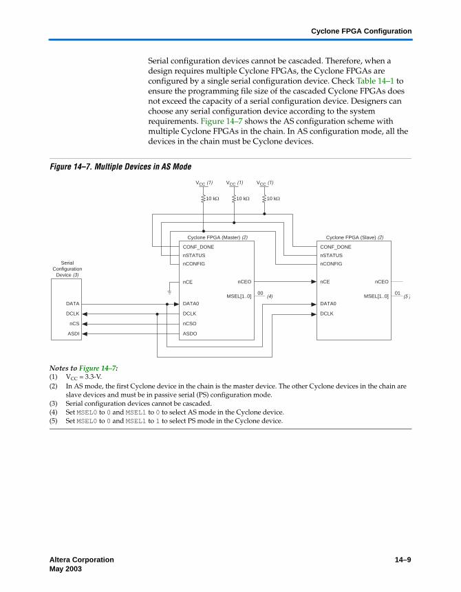
Altera Corporation 14–9May 2003 Preliminary
Cyclone FPGA Configuration
Serial configuration devices cannot be cascaded. Therefore, when a design requires multiple Cyclone FPGAs, the Cyclone FPGAs are configured by a single serial configuration device. Check Table 14–1 to ensure the programming file size of the cascaded Cyclone FPGAs does not exceed the capacity of a serial configuration device. Designers can choose any serial configuration device according to the system requirements. Figure 14–7 shows the AS configuration scheme with multiple Cyclone FPGAs in the chain. In AS configuration mode, all the devices in the chain must be Cyclone devices.
Figure 14–7. Multiple Devices in AS Mode
Notes to Figure 14–7:(1) VCC = 3.3-V.(2) In AS mode, the first Cyclone device in the chain is the master device. The other Cyclone devices in the chain are
slave devices and must be in passive serial (PS) configuration mode. (3) Serial configuration devices cannot be cascaded.(4) Set MSEL0 to 0 and MSEL1 to 0 to select AS mode in the Cyclone device.(5) Set MSEL0 to 0 and MSEL1 to 1 to select PS mode in the Cyclone device.
DATA
DCLK
nCS
ASDI
DATA0
DCLK
nCSO
nCE
nCONFIG
nSTATUS
MSEL[1..0]
nCEO
CONF_DONE
ASDO
VCC (1)
10 kΩ
VCC (1)
10 kΩ
VCC (1)
10 kΩ
(4)00
Cyclone FPGA (Master) (2)
DATA0
DCLK
nCE
nCONFIG
nSTATUS
MSEL[1..0]
nCEO
CONF_DONE
(5 )01
Cyclone FPGA (Slave) (2)
SerialConfiguration
Device (3)

14–10 Altera CorporationPreliminary May 2003
Cyclone Device Handbook, Volume 1
Figure 14–8 shows the timing waveform for Cyclone FPGA AS configuration scheme using a serial configuration device.
Figure 14–8. AS Configuration Timing
Table 14–6 shows the timing parameters for AS configuration mode.
Read Address
bit N − 1bit N bit 1 bit 0
tH
tCL
tCH
tSU
136 Cycles
nSTATUS
nCONFIG
CONF_DONE
nCSO
DCLK
ASDO
DATA0
INIT_DONE
User I/O User Mode
tPOR
Table 14–6. Timing Parameters for AS Configuration
Symbol Parameter Min Typ Max Unit
fCLK DCLK frequency (from Cyclone FPGA) 15 20 MHz
tCH DCLK high time 25 ns
tCL DCLK low time 25 ns
tH Data hold time after rising edge on DCLK 0 ns
tSU Data set up time before rising edge on DCLK 5 ns
tPOR POR delay 100 ms
Altera Corporation 14–11May 2003 Preliminary
Power & Operation
Power & Operation
This section describes the power modes, power-on reset (POR) delay, error detection, and initial programming state of serial configuration devices.
Power Mode
Serial configuration devices support active power and standby power modes. When nCS is low, the device is enabled and is in active power mode. The Cyclone FPGA is configured while in active power mode. When nCS is high, the device is disabled but could remain in active power mode until all internal cycles have completed (such as program or erase operations). The serial configuration device then goes into stand-by power mode. The ICC1 parameter specifies the VCC supply current when the device is in active power mode and the ICC0 parameter specifies the current when the device is in stand-by power mode (see Table 14–10).
Power-On Reset
During initial power-up, a POR delay occurs to help stabilize the system voltage levels. In AS configuration, the Cyclone FPGA controls the configuration and has a longer POR delay than the serial configuration device. Therefore, the POR delay is governed by the Cyclone FPGA (typically 100 ms).
Error Detection
In AS configuration with the serial configuration device, the Cyclone FPGA monitors the configuration status through the nSTATUS and CONF_DONE pins. If an error condition occurs (nSTATUS driven low) or if the CONF_DONE pin does not go high, the Cyclone FPGA will initiate reconfiguration by pulsing the nSTATUS and nCSO signals, which controls the chip select pin on the serial configuration device (nCS).
After an error, configuration automatically restarts if the Auto-Restart Upon Frame Error option is turned on in the Quartus II software.

14–12 Altera CorporationPreliminary May 2003
Cyclone Device Handbook, Volume 1
Operating Conditions
Tables 14–7 through 14–11 provide information on absolute maximum ratings, recommended operating conditions, DC operating conditions, and capacitance for serial configuration devices.
Table 14–7. Absolute Maximum Ratings Note (1)
Symbol Parameter Condition Min Max Unit
VCC Supply voltage With respect to ground −0.6 4.0 V
VI DC input voltage With respect to ground −0.6 4.0 V
IMAX DC VCC or GND current 15 mA
IOUT DC output current per pin −25 25 mA
PD Power dissipation 54 mW
TSTG Storage temperature No bias −65 150 °C
TAMB Ambient temperature Under bias −65 135 °C
TJ Junction temperature Under bias 135 °C
Table 14–8. Recommended Operating Conditions
Symbol Parameter Conditions Min Max Unit
VCC Supply voltage (2) 3.0 3.6 V
VI Input voltage Respect to GND −0.3 0.3 + VCC V
VO Output voltage 0 VCC V
TA Operating temperature For commercial use 0 70 °C
For industrial use −40 85 °C
tR Input rise time 5 ns
tF Input fall time 5 ns
Table 14–9. DC Operating Conditions
Symbol Parameter Conditions Min Max Unit
VIH High-level input voltage 0.7 × VCC VCC + 0.4 V
VIL Low-level input voltage −0.5 0.3 × VCC V
VOH High-level output voltage IOH = −100 µA (3) VCC − 0.2 V
VOL Low-level output voltage IOL = 1.6 mA (3) 0.4 V
II Input leakage current VI = VCC or GND −10 10 µA
IOZ Tri-state output off-state current VO = VCC or GND −10 10 µA

Altera Corporation 14–13May 2003 Preliminary
Package
Package All serial configuration devices are available in 8-pin plastic SOIC package. Figure 14–9 shows the mechanical drawing and specifications for this package.
f For more information on Altera device packaging, see Chapter 6, Package Information for Cyclone Devices.
Table 14–10. ICC Supply Current
Symbol Parameter Conditions Min Max Unit
ICC0 VCC supply current (standby) 50 µA
ICC1 VCC supply current (during active power mode)
5 14 mA
Table 14–11. Capacitance Note (4)
Symbol Parameter Conditions Min Max Unit
CIN Input pin capacitance VIN = 0 V 6 pF
COUT Output pin capacitance VOUT = 0 V 8 pF
Notes to Table 14–7 through 14–11:(1) See the Operating Requirements for Altera Devices Data Sheet.(2) Maximum VCC rise time is 100 ms.(3) The IOH parameter refers to high-level TTL or CMOS output current; the I OL parameter refers to low-level TTL or
CMOS output current.(4) Capacitance is sample-tested only at TA = 25 °C and at a 20-MHz frequency.

14–14 Altera CorporationPreliminary May 2003
Cyclone Device Handbook, Volume 1
Figure 14–9. 8-Pin SOIC Serial Configuration Device Package Notes (1), (2)
Notes to Figure 14–9:(1) All dimensions and tolerances conform to ANSI Y14.5M - 1982.(2) JEDEC reference MS-013 option AE.
Ordering Code Table 14–12 shows the ordering codes for serial configuration devices.
Pin 1
Symbol
h
Dimentions (mm)
Min. Nom. Max.1.35_
___
0.251.75
0.100.33 0.510.19 0.25
AA1BCDEeH
LN
__ 4.80
_
__
_
3.80
5.800.250.40
0 C 8 C
5.004.00
6.200.50
1.27 BSC
0.908
A
A1 B
D
EH
e
h × 45
C
L
8
8
N
SeatingPlane
o
o o
Table 14–12. Serial Configuration Device Ordering Codes
Device Ordering Code
EPCS1 EPCS1SI8
EPCS4 EPCS4SI8

Altera Corporation Index–1Preliminary
Index
1.5-V DevicesBoard Layout 12–21Choose a Regulator Type 12–9Designing with 12–1Linear Voltage Regulators 12–4Maximum Output Current 12–8Power Sequencing & Hot Socketing 12–1Regulator Application Examples 12–19Regulator Circuits 12–10Selecting Voltage Regulators 12–8Split-Plane Method 12–23Switching Voltage Regulators 12–6Synchronous Switching Regulator
Example 12–20Using MultiVolt I/O Pins 12–2Voltage Divider Network 12–10Voltage Regulators 12–3
AArchitecture
addnsub Signal 2–7Bus Hold 2–51Byte Enables 2–23Carry-Select Chain 2–10Clear & Preset Logic Control 2–12Clock
Clock Feedback 2–37Clock Mode
Independent 2–25Input/Output 2–25Read/Write 2–27
Clock Multiplication & Division 2–35Dual-Purpose Clock Pins 2–30External Clock Inputs 2–36External Clock Outputs 2–36Global Clock Network 2–29Global Clock Network & Phase-Locked
Loops 2–29Maximum Input & Output Clock
Rates 4–27
Phase Shifting 2–37Combined Resources 2–31Configuration
3–5Schemes 3–6Testing 3–1
Control Signals 2–38Control Signals & M4K Interface 2–23Cyclone Architecture 2–1DC & Switching Characteristics 4–1Device Pin-Outs 5–1Dynamic Arithmetic Mode 2–9Embedded Memory 2–18Functional Description 2–1I/O Standard
Advanced I/O Standard Support 2–52External I/O Delay Parameters 4–21I/O Structure 2–39LVDS I/O Pins 2–54MultiVolt I/O Interface 2–54
IEEE Std. 1149.1 (JTAG) Boundary Scan Support 3–1
LABControl Signals 2–4Interconnects 2–3
Lock Detect Signal 2–37Logic Array Blocks 2–3Logic Elements
2–5Operating Modes 2–7
LUT Chain & Register Chain 2–7Memory
Configuration Sizes 2–21DDR SDRAM & FCRAM 2–46External RAM Interfacing 2–46Modes 2–18
MultiTrack Interconnect 2–12Normal Mode 2–8Open-Drain Output 2–50Operating Conditions 4–1Operating Modes 3–6
Index–2 Altera CorporationPreliminary
Cyclone FPGA Device Handbook
Ordering Information 5–1Parity Bit Support 2–20PLLs 2–32Power Consumption 4–8Power Sequencing & Hot Socketing 2–55Programmable Drive Strength 2–49Programmable Duty Cycle 2–38Programmable Pull-Up Resistor 2–51Reference & Ordering Information 5–1Shift Register Support 2–20SignalTap II Embedded Logic Analyzer 3–5Single-Port Mode 2–28Slew-Rate Control 2–50Software 5–1Timing
External Timing Parameters 4–14Internal Timing Parameters 4–10Model 4–9Preliminary & Final 4–9
CConfiguration
Active Serial & JTAG 13–39Active Serial Configuration (Serial Configu-
ration Devices) 13–7Combining Configuration Schemes 13–39Configuring Cyclone
FPGAs 13–1FPGAs with JRunner 13–31FPGAs with the MicroBlaster
Software 13–23Configuring Multiple Cyclone
FPGAs 13–16Configuring Multiple Devices
(Cascading) 13–9Connecting the JTAG Chain to the Embedded
Processor 13–30Data Compression 13–3Device Configuration
Overview 13–1Device Configuration Files 13–47Device Options 13–41Jam
Example Jam File that Reads the IDCODE 13–38
Instructions 13–37STAPL 13–32
JTAG Configuration of Multiple Devices 13–28
JTAG Configuration Using a Download Cable 13–26
JTAG-Based Configuration 13–25Passive Serial 13–13Passive Serial & JTAG 13–40Program Flow 13–32Programming Configuration Devices 13–17Programming Serial Configuration
Devices 13–11PS Configuration from a
Microprocessor 13–22PS Configuration Using a Download
Cable 13–18PS Configuration using Configuration
Device 13–13Quartus II Software
Board Layout Tips 13–50Configuration Reliability 13–49Hexadecimal (Intel-Format) File
(.hex) 13–48Jam Byte-Code File (.jbc) 13–49Jam File (.jam) 13–49Programmer Object File (.pof) 13–48Raw Binary File (.rbf) 13–48SRAM Object File (.sof) 13–47Tabular Text File (.ttf) 13–48
Schemes 13–6Timing
Passive Serial Timing 13–23
DDevice Configuration Pins 13–45
II/O Standards
11–11.5-V
LVCMOS Normal & Wide Voltage Ranges (EIA/JEDEC Standard JESD8-11) 8–5

Altera Corporation Index–3Preliminary
1.8-VLVCMOS Normal & Wide Voltage Ranges
(EIA/JEDEC Standard EIA/JESD8-7) 8–4
LVTTL Normal & Wide Voltage Ranges (EIA/JEDEC Standard EIA/JESD8-7) 8–4
2.5-VLVCMOS Normal & Wide Voltage Ranges
(EIA/JEDEC Standard EIA/JESD8-5) 8–4
LVTTL Normal & Wide Voltage Ranges (EIA/JEDEC Standard EIA/JESD8-5) 8–3
3.3-V(PCI Special Interest Group (SIG) PCI Lo-
cal Bus Specification Revision 2.2) 8–5
LVCMOS (EIA/JEDEC Standard JESD8-B) 8–3
LVTTL (EIA/JEDEC Standard JESD8-B) 8–2
Bidirectional Pads 8–14Cyclone I/O Banks 8–8DC Guidelines 8–16Differential I/O Standard Termination 8–13Differential Pad Placement Guidelines 8–13Differential SSTL-2 - EIA/JEDEC Standard
JESD8-9A 8–8Hot Socketing 8–12I/O Termination 8–12Input Pads 8–14LVDS (ANSI/TIA/EIA Standard AN-
SI/TIA/EIA-644) 8–7Output Pads 8–14Pad Placement & DC Guidelines 8–13Programmable Current Drive Strength 8–11Quartus II Software
Assigning Pins 8–18Auto Placement & Verification of Select-
able I/O Standards 8–20Compiler Settings 8–17Device & Pin Options 8–17I/O Banks in the Floorplan View 8–19Programmable Drive Strength
Settings 8–19Software Support 8–17
SSTL-2 Class I & II (EIA/JEDEC Standard JESD8-9A) 8–6
SSTL-3 Class I & II (EIA/JEDEC Standard JESD8-8) 8–5
Supported I/O Standards 8–2Using Selectable I/O Standards in Cyclone
Devices 8–1Voltage-Referenced I/O Standard
Termination 8–13Voltages
5.0-V Device Compatibility 11–3Devices Can Be Driven before Power-
Up 11–6Hot-Socketing 11–6I/O Pins Remain Tri-Stated during Power-
Up 11–6MultiVolt I/O Operation 11–2Power-On Reset 11–7Power-Up Sequence 11–7Signal Pins Do Not Drive the VCCIO or
VCCINT Power Supplies 11–6VREF Pad Placement Guidelines 8–13
LLVDS
Clock Domains 9–3Cyclone I/O Banks 9–1Cyclone I/O Interface 9–3Cyclone Receiver & Transmitter
Termination 9–8Implementing LVDS in Cyclone
Devices 9–1Quartus II Software
Board Design Considerations 9–17Capturing Serial Data on Cyclone LVDS
Inputs 9–14Design Guidelines 9–16Differential Pad Placement
Guidelines 9–17Implementing Cyclone LVDS I/O Pins in
the Quartus II Software 9–10Receiver Circuit 9–15Transmitter Circuit 9–13Transmitting Serial Data on Cyclone LVDS
Outputs 9–10Receiver & Transmitter 9–4

Index–4 Altera CorporationPreliminary
Cyclone FPGA Device Handbook
Timing in Cyclone Devices 9–7
MMemory
Bidirectional Double Data Rate 10–3DDR Memory Support 10–4Double Data Rate
Input 10–1Output 10–2
Implementing Double Data Rate I/O Signal-ing in Cyclone Devices 10–1
PPLL
altpllCompilation Report 6–31Input Ports 6–22MegaWizard Customization 6–23MegaWizard Page Description 6–25Output Ports 6–23Simulation 6–37Timing Analysis 6–33
areset 6–12Board Layout 6–17Clock
Combined Sources 6–41Dedicated Clock Input Pins 6–40Dual-Purpose Clock I/O Pins 6–40External Clock Output 6–11Feedback Modes 6–13Global Clock Network 6–38Multiplication & Division 6–8
Control Signals 6–12Cyclone PLL Blocks 6–2Hardware Features 6–8Hardware Overview 6–1Jitter Considerations 6–19Modes
No Compensation 6–15Normal 6–13
Zero Delay Buffer 6–14Partitioned VCCA Island within VCCINT
Plane 6–17pfdena 6–12Phase Shifting 6–9Pins 6–16Pins & Clock Network Connections 6–6pllena 6–12Programmable Duty Cycle 6–10Quartus II altpll Megafunction 6–21Separate VCCA Power Plane 6–17Software Support 6–21Specifications 6–20Thick VCCA Traces 6–18Using PLLs in Cyclone Devices 6–1VCCA & GNDA 6–17
SSerial Configuration Devices
(EPCS1 & EPCS4) Data Sheet 14–1Accessing Memory 14–3Cyclone FPGA Configuration 14–7Error Detection 14–11Features 14–1Functional Description 14–2Operating Conditions 14–12Ordering Code 14–14Package 14–13Pin Description 14–4Power & Operation 14–11Power Mode 14–11Power-On Reset 14–11Programming & Configuration File
Support 14–4Software Overview 6–4
UUsing Cyclone Devices in Multiple-Voltage
Systems 11–1

Preliminary Information101 Innovation DriveSan Jose, CA 95134(408) 544-7000http://www.altera.com
Cyclone Device Handbook, Volume 2
C5V2-1.0

Copyright © 2003 Altera Corporation. All rights reserved. Altera, The Programmable Solutions Company, the stylized Altera logo, specific device des-ignations, and all other words and logos that are identified as trademarks and/or service marks are, unless noted otherwise, the trademarks andservice marks of Altera Corporation in the U.S. and other countries. All other product or service names are the property of their respective holders. Al-tera products are protected under numerous U.S. and foreign patents and pending applications, maskwork rights, and copyrights. Altera warrantsperformance of its semiconductor products to current specifications in accordance with Altera's standard warranty, but reserves the right to makechanges to any products and services at any time without notice. Altera assumes no responsibility or liability arising out of the ap-plication or use of any information, product, or service described herein except as expressly agreed to in writing by AlteraCorporation. Altera customers are advised to obtain the latest version of device specifications before relying on any published in-formation and before placing orders for products or services.
Printed on recycled paper
ii Altera CorporationPreliminary

Altera Corporation
Contents
Chapter Revision Dates .......................................................................... iii
About this Handbook ............................................................................. xiiiHow to Find Information ..................................................................................................................... xiiiHow to Contact Altera .......................................................................................................................... xiiiTypographic Conventions .................................................................................................................... xiv
Section I. PCB Layout GuidelinesRevision History ....................................................................................................................... Section I–1
Chapter 1. Cyclone EP1C3T100 Device Pin InformationIntroduction ............................................................................................................................................ 1–1Pin List ..................................................................................................................................................... 1–2Pin Definitions ........................................................................................................................................ 1–7PLL & Bank Diagram .......................................................................................................................... 1–10
Chapter 2. Cyclone EP1C3T144 Device Pin InformationIntroduction ............................................................................................................................................ 2–1Pin List ..................................................................................................................................................... 2–2Pin Definitions ........................................................................................................................................ 2–9PLL & Bank Diagram .......................................................................................................................... 2–13
Chapter 3. Cyclone EP1C6 Device Pin InformationIntroduction ............................................................................................................................................ 3–1Pin List ..................................................................................................................................................... 3–2Pin Definitions ...................................................................................................................................... 3–16PLL & Bank Diagram .......................................................................................................................... 3–20
Chapter 4. Cyclone EP1C12 Device Pin InformationIntroduction ............................................................................................................................................ 4–1Pin List ..................................................................................................................................................... 4–2Pin Definitions ...................................................................................................................................... 4–20PLL & Bank Diagram .......................................................................................................................... 4–24
Chapter 5. Cyclone EP1C20 Device Pin InformationIntroduction ............................................................................................................................................ 5–1Pin List ..................................................................................................................................................... 5–2
vPreliminary

Cyclone Device Handbook, Volume 2
Pin Definitions ...................................................................................................................................... 5–22PLL & Bank Diagram .......................................................................................................................... 5–26
Chapter 6. Package Information for Cyclone DevicesIntroduction ............................................................................................................................................ 6–1Device & Package Cross Reference ..................................................................................................... 6–1Thermal Resistance ................................................................................................................................ 6–2Package Outlines ................................................................................................................................... 6–2
100-Pin Plastic Thin Quad Flat Pack (TQFP) ................................................................................ 6–3144-Pin Plastic Thin Quad Flat Pack (TQFP) ................................................................................ 6–5240-Pin Plastic Quad Flat Pack (PQFP) ......................................................................................... 6–7256-Pin Non-Thermally Enhanced FineLine Ball-Grid Array ................................................... 6–9324-Pin Non-Thermally Enhanced FineLine Ball-Grid Array ................................................. 6–11400-Pin Non-Thermally Enhanced FineLine Ball-Grid Array ................................................. 6–13
Chapter 7. Designing with FineLine BGA PackagesIntroduction ............................................................................................................................................ 7–1Overview of BGA Packages ................................................................................................................. 7–1PCB Layout Terminology ..................................................................................................................... 7–2
Escape Routing ................................................................................................................................. 7–2Multi-Layer PCBs ............................................................................................................................. 7–2Vias ..................................................................................................................................................... 7–2Via Capture Pad ............................................................................................................................... 7–4Surface Land Pad .............................................................................................................................. 7–4Stringer ............................................................................................................................................... 7–5
PCB Layout for FineLine BGA Packages ........................................................................................... 7–6Surface Land Pad Dimension ......................................................................................................... 7–6Via Capture Pad Layout & Dimension ......................................................................................... 7–7Signal Line Space & Trace Width ................................................................................................. 7–10Number of PCB Layers .................................................................................................................. 7–11
Conclusion ............................................................................................................................................ 7–12
1–vi Altera CorporationPreliminary

Altera Corporation
Chapter Revision Dates
The chapters in this book, Cyclone Device Handbook, Volume 2, were revised on the following dates. Where chapters or groups of chapters are available separately, part numbers are listed.
Chapter 1. Cyclone EP1C3T100 Device Pin InformationRevised: May 2003Part number: C52001-1.0
Chapter 2. Cyclone EP1C3T144 Device Pin InformationRevised: May 2003Part number: C52002-1.0
Chapter 3. Cyclone EP1C6 Device Pin InformationRevised: May 2003Part number: C52003-1.0
Chapter 4. Cyclone EP1C12 Device Pin InformationRevised: May 2003Part number: C52004-1.0
Chapter 5. Cyclone EP1C20 Device Pin InformationRevised: May 2003Part number: C52005-1.0
Chapter 6. Package Information for Cyclone DevicesRevised: May 2003Part number: C52006-1.0
Chapter 7. Designing with FineLine BGA PackagesRevised: May 2003Part number: C52007-1.0
iiiPreliminary

Cyclone Device Handbook, Volume 2
1–iv Altera CorporationPreliminary

Altera Corporation
About this Handbook
This handbook provides comprehensive information about the Altera® Cyclone family of devices.
How to Find Information
You can find more information in the following ways:
The Adobe Acrobat Find feature, which searches the text of a PDF document. Click the binoculars toolbar icon to open the Find dialog box.
Acrobat bookmarks, which serve as an additional table of contents in PDF documents.
Thumbnail icons, which provide miniature previews of each page, provide a link to the pages.
Numerous links, shown in green text, which allow you to jump to related information.
How to Contact Altera
For the most up-to-date information about Altera products, go to the Altera world-wide web site at www.altera.com. For technical support on this product, go to www.altera.com/mysupport. For additional information about Altera products, consult the sources shown below.
Information Type USA & Canada All Other Locations
Technical support www.altera.com/mysupport/ altera.com/mysupport/
(800) 800-EPLD (3753)(7:00 a.m. to 5:00 p.m. Pacific Time)
(408) 544-7000 (1)(7:00 a.m. to 5:00 p.m. Pacific Time)
Product literature www.altera.com www.altera.com
Altera literature services [email protected] (1) [email protected] (1)
Non-technical customer service
(800) 767-3753 (408) 544-7000 (7:30 a.m. to 5:30 p.m. Pacific Time)
FTP site ftp.altera.com ftp.altera.com
Note to table:(1) You can also contact your local Altera sales office or sales representative.
xiiiPreliminary

Cyclone Device Handbook, Volume 2
Typographic Conventions
This document uses the typographic conventions shown below.
Visual Cue Meaning
Bold Type with Initial Capital Letters
Command names, dialog box titles, checkbox options, and dialog box options are shown in bold, initial capital letters. Example: Save As dialog box.
bold type External timing parameters, directory names, project names, disk drive names, filenames, filename extensions, and software utility names are shown in bold type. Examples: fMAX, \qdesigns directory, d: drive, chiptrip.gdf file.
Italic Type with Initial Capital Letters
Document titles are shown in italic type with initial capital letters. Example: AN 75: High-Speed Board Design.
Italic type Internal timing parameters and variables are shown in italic type. Examples: tPIA, n + 1.
Variable names are enclosed in angle brackets (< >) and shown in italic type. Example: <file name>, <project name>.pof file.
Initial Capital Letters Keyboard keys and menu names are shown with initial capital letters. Examples: Delete key, the Options menu.
“Subheading Title” References to sections within a document and titles of on-line help topics are shown in quotation marks. Example: “Typographic Conventions.”
Courier type Signal and port names are shown in lowercase Courier type. Examples: data1, tdi, input. Active-low signals are denoted by suffix n, e.g., resetn.
Anything that must be typed exactly as it appears is shown in Courier type. For example: c:\qdesigns\tutorial\chiptrip.gdf. Also, sections of an actual file, such as a Report File, references to parts of files (e.g., the AHDL keyword SUBDESIGN), as well as logic function names (e.g., TRI) are shown in Courier.
1., 2., 3., anda., b., c., etc.
Numbered steps are used in a list of items when the sequence of the items is important, such as the steps listed in a procedure.
• Bullets are used in a list of items when the sequence of the items is not important.
v The checkmark indicates a procedure that consists of one step only.
1 The hand points to information that requires special attention.
r The angled arrow indicates you should press the Enter key.
f The feet direct you to more information on a particular topic.
1–xiv Altera CorporationPreliminary

Altera Corporation
Section I. PCB LayoutGuidelines
This section provides information for board layout designers to successfully layout their boards for Cyclone devices. It contains the required PCB layout guidelines, device pin tables, and package specifications.
This section includes the following chapters:
Chapter 1. Cyclone EP1C3T100 Device Pin Information
Chapter 2. Cyclone EP1C3T144 Device Pin Information
Chapter 3. Cyclone EP1C6 Device Pin Information
Chapter 4. Cyclone EP1C12 Device Pin Information
Chapter 5. Cyclone EP1C20 Device Pin Information
Chapter 6. Package Information for Cyclone Devices
Chapter 7. Designing with FineLine BGA Packages
Revision History The table below shows the revision history for Chapter 7.
Chapter(s) Date / Version Changes Made
12 May 2003v1.0
Updated Table 7–6.
v1.03 Updated the “PCB Layout for FineLine BGA Packages” section and Table 7–6.
v1.02 Minor updates.
v1.01 Updated Table 7–6.
Section I–1Preliminary

PCB Layout Guidelines Cyclone Device Handbook, Volume 2
Section I–2 Altera CorporationPreliminary

Altera Corporation May 2003
C52001-1.0
1. Cyclone EP1C3T100Device Pin Information
Introduction The following tables contain pin information for the Cyclone EP1C3T100 device, organized into the following sections:
Section Page
Pin List. . . . . . . . . . . . . . . . . . . . . . . . . . . . . . . . . . . . . . . . . . . . . . 1–2Pin Definitions . . . . . . . . . . . . . . . . . . . . . . . . . . . . . . . . . . . . . . . 1–7PLL & Bank Diagram . . . . . . . . . . . . . . . . . . . . . . . . . . . . . . . . 1–10
1–1Preliminary

Cyclone Device Handbook, Volume 2
Pin
List
Tabl
e1–
1 sh
ows
the
com
ple
te p
in li
st fo
r th
e C
yclo
ne E
P1C
3T10
0 d
evic
e:
Tabl
e1–
1.Pi
n Li
st fo
r the
Cyc
lone
EP1
C3T1
00 D
evic
e (P
art1
of5)
Dev
ice
Pack
age
DQS
for X
8 in
10
0-Pi
n Th
in Q
uad
Flat
Pac
kPi
n Na
me
/ Fu
nctio
nOp
tiona
l Fu
nctio
n(s)
Conf
igur
atio
n Fu
nctio
nBa
nk N
umbe
rVR
EF B
ank
100-
Pin
Thin
Qua
d Fl
at P
ack
IOIN
IT_D
ON
EB
1V
RE
F0B
11
IOB
1V
RE
F0B
12
IOC
LKU
SR
B1
VR
EF
0B1
3
IOV
RE
F0B
1B
1V
RE
F0B
14
VC
CIO
1B
1V
RE
F0B
1
GN
DB
1V
RE
F0B
1
IOV
RE
F1B
1B
1V
RE
F1B
15
IOnC
SO
B1
VR
EF
1B1
6
DA
TA0
DA
TA0
B1
VR
EF
1B1
7
nCO
NF
IGnC
ON
FIG
B1
VR
EF
1B1
8
VC
CA
_PLL
1V
RE
F1B
19
CLK
0B
1V
RE
F1B
110
GN
DA
_PLL
1V
RE
F1B
111
nCE
OnC
EO
B1
VR
EF
1B1
12
nCE
nCE
B1
VR
EF
1B1
13
MS
EL0
MS
EL0
B1
VR
EF
1B1
14
MS
EL1
MS
EL1
B1
VR
EF
1B1
15
DC
LKD
CLK
B1
VR
EF
1B1
16
IOA
SD
OB
1V
RE
F1B
117
VC
CIO
1B
1V
RE
F2B
118
GN
DB
1V
RE
F2B
119
1–2 Altera CorporationPreliminary May 2003

Pin List
IOV
RE
F2B
1B
1V
RE
F2B
120
IOB
1V
RE
F2B
121
IOB
1V
RE
F2B
122
IOB
1V
RE
F2B
123
IOB
1V
RE
F2B
124
IOB
1V
RE
F2B
125
IOB
4V
RE
F2B
426
IOB
4V
RE
F2B
427
DQ
1B7
IOB
4V
RE
F2B
428
DQ
1B6
IOB
4V
RE
F2B
429
DQ
1B5
GN
DB
4V
RE
F2B
430
VC
CIO
4B
4V
RE
F2B
431
GN
DV
RE
F2B
432
VC
CIN
TV
RE
F2B
433
IOD
PC
LK7
B4
VR
EF
2B4
34D
QS
1B
IOV
RE
F2B
4B
4V
RE
F2B
435
IOB
4V
RE
F2B
436
DQ
1B4
IOB
4V
RE
F1B
437
IOV
RE
F1B
4B
4V
RE
F1B
438
IOB
4V
RE
F1B
439
DM
1B
IOB
4V
RE
F1B
440
IOV
RE
F0B
4B
4V
RE
F0B
441
IOD
PC
LK6
B4
VR
EF
0B4
42
Tabl
e1–
1.Pi
n Li
st fo
r the
Cyc
lone
EP1
C3T1
00 D
evic
e (P
art2
of5)
Dev
ice
Pack
age
DQS
for X
8 in
10
0-Pi
n Th
in Q
uad
Flat
Pac
kPi
n Na
me
/ Fu
nctio
nOp
tiona
l Fu
nctio
n(s)
Conf
igur
atio
n Fu
nctio
nBa
nk N
umbe
rVR
EF B
ank
100-
Pin
Thin
Qua
d Fl
at P
ack
Altera Corporation 1–3May 2003 Preliminary

Cyclone Device Handbook, Volume 2
GN
DV
RE
F0B
443
VC
CIN
TV
RE
F0B
444
GN
DB
4V
RE
F0B
445
VC
CIO
4B
4V
RE
F0B
446
IOB
4V
RE
F0B
447
DQ
1B3
IOB
4V
RE
F0B
448
DQ
1B2
IOB
4V
RE
F0B
449
DQ
1B1
IOB
4V
RE
F0B
450
DQ
1B0
IOB
3V
RE
F2B
351
IOB
3V
RE
F2B
352
IOB
3V
RE
F2B
353
DQ
0R7
IOB
3V
RE
F2B
354
DQ
0R6
IOB
3V
RE
F2B
355
DQ
0R5
IOB
3V
RE
F2B
356
DQ
0R4
IOV
RE
F2B
3B
3V
RE
F2B
357
GN
DB
3V
RE
F2B
358
VC
CIO
3B
3V
RE
F2B
359
CO
NF
_DO
NE
CO
NF
_DO
NE
B3
VR
EF
1B3
60
nSTA
TU
SnS
TAT
US
B3
VR
EF
1B3
61
TC
KT
CK
B3
VR
EF
1B3
62
TM
ST
MS
B3
VR
EF
1B3
63
TD
OT
DO
B3
VR
EF
1B3
64
IOB
3V
RE
F1B
365
DM
0R
Tabl
e1–
1.Pi
n Li
st fo
r the
Cyc
lone
EP1
C3T1
00 D
evic
e (P
art3
of5)
Dev
ice
Pack
age
DQS
for X
8 in
10
0-Pi
n Th
in Q
uad
Flat
Pac
kPi
n Na
me
/ Fu
nctio
nOp
tiona
l Fu
nctio
n(s)
Conf
igur
atio
n Fu
nctio
nBa
nk N
umbe
rVR
EF B
ank
100-
Pin
Thin
Qua
d Fl
at P
ack
1–4 Altera CorporationPreliminary May 2003

Pin List
CLK
2B
3V
RE
F1B
366
TD
IT
DI
B3
VR
EF
1B3
67
IOV
RE
F1B
3B
3V
RE
F1B
368
IOB
3V
RE
F0B
369
DQ
0R3
IOB
3V
RE
F0B
370
DQ
0R2
IOB
3V
RE
F0B
371
DQ
0R1
IOD
PC
LK4
B3
VR
EF
0B3
72D
QS
0R
GN
DB
3V
RE
F0B
3
VC
CIO
3B
3V
RE
F0B
3
IOV
RE
F0B
3B
3V
RE
F0B
373
IOB
3V
RE
F0B
374
DQ
0R0
IOB
3V
RE
F0B
375
IOB
2V
RE
F0B
276
DQ
1T0
IOB
2V
RE
F0B
277
DQ
1T1
IOB
2V
RE
F0B
278
DQ
1T2
IOB
2V
RE
F0B
279
DQ
1T3
VC
CIO
2B
2V
RE
F0B
280
GN
DB
2V
RE
F0B
281
VC
CIN
TV
RE
F0B
282
GN
DV
RE
F0B
283
IOD
PC
LK3
B2
VR
EF
0B2
84
IOV
RE
F0B
2B
2V
RE
F0B
285
IOB
2V
RE
F1B
286
Tabl
e1–
1.Pi
n Li
st fo
r the
Cyc
lone
EP1
C3T1
00 D
evic
e (P
art4
of5)
Dev
ice
Pack
age
DQS
for X
8 in
10
0-Pi
n Th
in Q
uad
Flat
Pac
kPi
n Na
me
/ Fu
nctio
nOp
tiona
l Fu
nctio
n(s)
Conf
igur
atio
n Fu
nctio
nBa
nk N
umbe
rVR
EF B
ank
100-
Pin
Thin
Qua
d Fl
at P
ack
Altera Corporation 1–5May 2003 Preliminary

Cyclone Device Handbook, Volume 2
IOB
2V
RE
F1B
287
IOV
RE
F1B
2B
2V
RE
F1B
288
IOB
2V
RE
F1B
289
IOB
2V
RE
F2B
290
DM
1T
IOV
RE
F2B
2B
2V
RE
F2B
291
IOD
PC
LK2
B2
VR
EF
2B2
92D
QS
1T
VC
CIN
TV
RE
F2B
293
GN
DV
RE
F2B
294
VC
CIO
2B
2V
RE
F2B
295
GN
DB
2V
RE
F2B
296
IOB
2V
RE
F2B
297
DQ
1T4
IOB
2V
RE
F2B
298
DQ
1T5
IOD
EV
_OE
B2
VR
EF
2B2
99D
Q1T
6
IOD
EV
_CLR
nB
2V
RE
F2B
210
0D
Q1T
7
Tabl
e1–
1.Pi
n Li
st fo
r the
Cyc
lone
EP1
C3T1
00 D
evic
e (P
art5
of5)
Dev
ice
Pack
age
DQS
for X
8 in
10
0-Pi
n Th
in Q
uad
Flat
Pac
kPi
n Na
me
/ Fu
nctio
nOp
tiona
l Fu
nctio
n(s)
Conf
igur
atio
n Fu
nctio
nBa
nk N
umbe
rVR
EF B
ank
100-
Pin
Thin
Qua
d Fl
at P
ack
1–6 Altera CorporationPreliminary May 2003

Pin Definitions
Pin
Defin
ition
sTa
ble
1–2
show
s p
in d
efin
itio
ns fo
r th
e E
P1C
3T10
0 d
evic
e.
Tabl
e1–
2.Pi
n De
finiti
ons
for t
he C
yclo
ne E
P1C3
T100
Dev
ice
(Pa
rt1
of3)
Pin
Nam
ePi
n Ty
pe (1
st, 2
nd, &
3rd
Fu
nctio
n)Pi
n D
escr
iptio
n
Supp
ly a
nd R
efer
ence
Pin
s
VC
CIO
[1..4
]P
ower
The
se a
re I/
O s
uppl
y vo
ltage
pin
s fo
r ban
ks 1
thro
ugh
4. E
ach
bank
can
sup
port
a
diffe
rent
vol
tage
leve
l. V
CC
IO s
uppl
ies
pow
er to
the
outp
ut b
uffe
rs fo
r al
l I/O
st
anda
rds.
VC
CIO
als
o su
pplie
s po
wer
to th
e in
put b
uffe
rs u
sed
for
the
LVT
TL,
LV
CM
OS
, 1.5
-V, 1
.8-V
, 2.5
-V, a
nd 3
.3-V
PC
I I/O
sta
ndar
ds.
VC
CIN
TP
ower
The
se a
re in
tern
al lo
gic
arra
y vo
ltage
sup
ply
pins
. VC
CIN
T a
lso
supp
lies
pow
er to
th
e in
put b
uffe
rs u
sed
for
the
LVD
S, S
ST
L2, a
nd S
ST
L3 I/
O s
tand
ards
.
VR
EF
[0..2
]B[1
..4]
I/O, I
nput
Inpu
t ref
eren
ce v
olta
ge fo
r ba
nks
1-4.
If a
ban
k us
es a
vol
tage
-ref
eren
ced
I/O
stan
dard
, the
n th
ese
pins
are
use
d as
the
volta
ge-r
efer
ence
pin
s fo
r th
e ba
nk. I
f vo
ltage
ref
eren
ce I/
O s
tand
ards
are
not
use
d in
the
bank
, the
VR
EF
pin
s ar
e av
aila
ble
as u
ser
I/O p
ins.
VC
CA
_PLL
[1..2
]P
ower
Ana
log
pow
er fo
r P
LLs[
1..2
]. T
he d
esig
ner
mus
t con
nect
this
pin
to 1
.5 V
, eve
n if
the
PLL
is n
ot u
sed.
GN
DA
_PLL
[1..2
]G
roun
dA
nalo
g gr
ound
for
PLL
s[1.
.2].
The
des
igne
r can
con
nect
this
pin
to th
e G
ND
pla
ne
on th
e bo
ard.
Conf
igur
atio
n an
d JT
AG P
ins
CO
NF
_DO
NE
Bid
irect
iona
l (op
en-d
rain
)T
his
is a
ded
icat
ed c
onfig
urat
ion
stat
us p
in; i
t is
not a
vaila
ble
as a
use
r I/O
pin
.
nSTA
TU
SB
idire
ctio
nal (
open
-dra
in)
Thi
s is
a d
edic
ated
con
figur
atio
n st
atus
pin
; it i
s no
t ava
ilabl
e as
a u
ser
I/O p
in.
nCO
NF
IGIn
put
Ded
icat
ed c
onfig
urat
ion
cont
rol i
nput
. A lo
w tr
ansi
tion
rese
ts th
e ta
rget
dev
ice;
a
low
-to-
high
tran
sitio
n be
gins
con
figur
atio
n. A
ll I/O
pin
s tr
i-sta
te w
hen
nCO
NF
IG is
dr
iven
low
.
DC
LKIn
put (
PS
mod
e), O
utpu
t (A
S m
ode)
In p
assi
ve s
eria
l con
figur
atio
n m
ode,
DC
LK is
a c
lock
inpu
t use
d to
clo
ck
conf
igur
atio
n da
ta fr
om a
n ex
tern
al s
ourc
e in
to th
e C
yclo
ne d
evic
e. In
act
ive
seria
l co
nfig
urat
ion
mod
e, D
CLK
is a
clo
ck o
utpu
t fro
m th
e C
yclo
ne d
evic
e (t
he C
yclo
ne
devi
ce a
cts
as m
aste
r in
this
mod
e). T
his
is a
ded
icat
ed p
in u
sed
for
conf
igur
atio
n.
DA
TA0
Inpu
tD
edic
ated
con
figur
atio
n da
ta in
put p
in.
Altera Corporation 1–7May 2003 Preliminary

Cyclone Device Handbook, Volume 2
nCE
Inpu
tA
ctiv
e-lo
w c
hip
enab
le. D
edic
ated
chi
p en
able
inpu
t use
d to
det
ect w
hich
dev
ice
is
activ
e in
a c
hain
of d
evic
es. W
hen
nCE
is lo
w, t
he d
evic
e is
ena
bled
. Whe
n nC
E is
hi
gh, t
he d
evic
e is
dis
able
d.
nCE
OO
utpu
tO
utpu
t tha
t driv
es lo
w w
hen
devi
ce c
onfig
urat
ion
is c
ompl
ete.
Dur
ing
mul
ti-de
vice
co
nfig
urat
ion,
this
pin
feed
s a
subs
eque
nt d
evic
e’s
nCE
pin
.
AS
DO
I/O, O
utpu
tA
ctiv
e se
rial d
ata
outp
ut fr
om th
e C
yclo
ne d
evic
e. T
his
outp
ut p
in is
util
ized
dur
ing
activ
e se
rial c
onfig
urat
ion
mod
e. T
he C
yclo
ne d
evic
e co
ntro
ls c
onfig
urat
ion
and
driv
es a
ddre
ss a
nd c
ontr
ol in
form
atio
n ou
t on
AS
DO
. In
pass
ive
seria
l co
nfig
urat
ion,
this
pin
is a
vaila
ble
as a
use
r I/O
pin
.
nCS
OI/O
, Out
put
Chi
p se
lect
out
put t
hat e
nabl
es/d
isab
les
a se
rial c
onfig
urat
ion
devi
ce.
Thi
s ou
tput
is
util
ized
dur
ing
activ
e se
rial c
onfig
urat
ion
mod
e. T
he C
yclo
ne d
evic
e co
ntro
ls
conf
igur
atio
n an
d en
able
s th
e se
rial c
onfig
urat
ion
devi
ce b
y dr
ivin
g nC
SO
low
. In
pass
ive
seria
l con
figur
atio
n, th
is p
in is
ava
ilabl
e as
a u
ser
I/O p
in.
INIT
_DO
NE
I/O, O
utpu
t (op
en-d
rain
)T
his
is a
dua
l-pur
pose
pin
and
can
be
used
as
an I/
O p
in w
hen
not e
nabl
ed a
s IN
IT_D
ON
E. W
hen
enab
led,
the
pin
indi
cate
s w
hen
the
devi
ce h
as e
nter
ed u
ser
mod
e. T
his
pin
can
be u
sed
as a
use
r I/O
pin
afte
r co
nfig
urat
ion.
CLK
US
RI/O
, Inp
utO
ptio
nal u
ser-
supp
lied
cloc
k in
put.
Syn
chro
nize
s th
e in
itial
izat
ion
of o
ne o
r m
ore
devi
ces.
Thi
s pi
n ca
n be
use
d as
a u
ser
I/O p
in a
fter
conf
igur
atio
n.
DE
V_C
LRn
I/O, I
nput
Dua
l-pur
pose
pin
that
can
ove
rrid
e al
l cle
ars
on a
ll de
vice
regi
ster
s. W
hen
this
pin
is
driv
en lo
w, a
ll re
gist
ers
are
clea
red;
whe
n th
is p
in is
driv
en h
igh,
all
regi
ster
s be
have
as
defin
ed in
the
desi
gn.
DE
V_O
EI/O
, Inp
utD
ual-p
urpo
se p
in th
at c
an o
verr
ide
all t
ri-st
ates
on
the
devi
ce. W
hen
this
pin
is
driv
en lo
w, a
ll I/O
pin
s ar
e tr
i-sta
ted;
whe
n th
is p
in is
driv
en h
igh,
all
I/O p
ins
beha
ve
as d
efin
ed in
the
desi
gn.
MS
EL[
1..0
]In
put
Ded
icat
ed m
ode
sele
ct c
ontr
ol p
ins
that
set
the
conf
igur
atio
n m
ode
for
the
devi
ce.
TM
SIn
put
Thi
s is
a d
edic
ated
JTA
G in
put p
in.
TD
IIn
put
Thi
s is
a d
edic
ated
JTA
G in
put p
in.
TC
KIn
put
Thi
s is
a d
edic
ated
JTA
G in
put p
in.
TD
OO
utpu
tT
his
is a
ded
icat
ed J
TAG
out
put p
in.
Tabl
e1–
2.Pi
n De
finiti
ons
for t
he C
yclo
ne E
P1C3
T100
Dev
ice
(Pa
rt2
of3)
Pin
Nam
ePi
n Ty
pe (1
st, 2
nd, &
3rd
Fu
nctio
n)Pi
n D
escr
iptio
n
1–8 Altera CorporationPreliminary May 2003

Pin Definitions
Cloc
k an
d PL
L Pi
ns
CLK
0In
put
Ded
icat
ed g
loba
l clo
ck in
put.
The
dua
l-fun
ctio
n of
CLK
0 is
LV
DS
CLK
1p, w
hich
is
used
for
diffe
rent
ial i
nput
to P
LL1.
CLK
2In
put
Ded
icat
ed g
loba
l clo
ck in
put.
The
dua
l-fun
ctio
n of
CLK
2 is
LV
DS
CLK
2p, w
hich
is
used
for
diffe
rent
ial i
nput
to P
LL2.
DP
CLK
[7..0
]I/O
Dua
l-pur
pose
clo
ck p
ins
that
can
con
nect
to th
e gl
obal
clo
ck n
etw
ork.
The
se p
ins
can
be u
sed
for
high
fan-
out c
ontr
ol s
igna
ls, s
uch
as c
lock
s, c
lear
s, IR
DY,
TR
DY,
or
DQ
S s
igna
ls.
The
se p
ins
are
also
ava
ilabl
e as
use
r I/O
pin
s.
Dual
-Pur
pose
Ext
erna
l Mem
ory
Inte
rfac
e Pi
ns
DQ
S[0
..1][L
,R,T
,B]
I/OO
ptio
nal d
ata
stro
be s
igna
l for
use
in e
xter
nal m
emor
y in
terf
acin
g. T
hese
pin
s al
so
func
tion
as D
PC
LK p
ins;
ther
efor
e, th
e D
QS
sig
nals
can
con
nect
to th
e gl
obal
clo
ck
netw
ork.
A p
rogr
amm
able
del
ay c
hain
is u
sed
to s
hift
the
DQ
S s
igna
ls b
y 90
or 7
2 de
gree
s.
DQ
[0..7
][L,R
,T,B
]I/O
Opt
iona
l dat
a si
gnal
for
use
in e
xter
nal m
emor
y in
terf
acin
g.
DM
[0..1
][L,R
,T,B
]I/O
Opt
iona
l dat
a m
ask
outp
ut s
igna
l for
use
in e
xter
nal m
emor
y in
terf
acin
g.
Tabl
e1–
2.Pi
n De
finiti
ons
for t
he C
yclo
ne E
P1C3
T100
Dev
ice
(Pa
rt3
of3)
Pin
Nam
ePi
n Ty
pe (1
st, 2
nd, &
3rd
Fu
nctio
n)Pi
n D
escr
iptio
n
Altera Corporation 1–9May 2003 Preliminary

Cyclone Device Handbook, Volume 2
PLL & Bank Diagram
Figure 1–1 shows the PLL and Bank locations for the EP1C3T100 device.
Figure 1–1. PLL and Bank Diagram (1), (2)
Notes for Figure 1–1:(1) This is a top view of the silicon die. (2) This is a pictoral representation only to get an idea of placement on the device. Refer to the pin-list and
VR
EB
2B3
B4VREF2B4 VREF1B4 VREF0B4
B3
VR
EF
0B3
VR
EF
1B3
VREF2B2 VREF1B2 VREF0B2
B2
VR
EF
0B1
B1
VR
EF
1B1
PLL1
VR
EB
2B1
1–10 Altera CorporationPreliminary May 2003

Altera Corporation May 2003
C52002-1.0
2. Cyclone EP1C3T144Device Pin Information
Introduction The following tables contain pin information for the Cyclone EP1C3T144 device, organized into the following sections:
Section Page
Pin List. . . . . . . . . . . . . . . . . . . . . . . . . . . . . . . . . . . . . . . . . . . . . . 2–2Pin Definitions . . . . . . . . . . . . . . . . . . . . . . . . . . . . . . . . . . . . . . . 2–9PLL & Bank Diagram . . . . . . . . . . . . . . . . . . . . . . . . . . . . . . . . 2–13
2–1Preliminary

Cyclone Device Handbook, Volume 2
Pin
List
Tabl
e2–
1 sh
ows
the
com
ple
te p
in li
st fo
r th
e C
yclo
ne E
P1C
3T14
4 d
evic
e:
Tabl
e2–
1.Pi
n Li
st fo
r the
Cyc
lone
EP1
C3T1
44 D
evic
e (P
art1
of7)
Dev
ice
Pack
age
DQS
for X
8 in
14
4-Pi
n Th
in Q
uad
Flat
Pac
kPi
n Na
me/
Fu
nctio
nOp
tiona
l Fu
nctio
n(s)
Conf
igur
atio
n Fu
nctio
nBa
nk N
umbe
rVR
EF B
ank
144-
Pin
Thin
Qua
d Fl
at P
ack
IOLV
DS
4pIN
IT_D
ON
EB
1V
RE
F0B
11
DM
1L
IOLV
DS
4nB
1V
RE
F0B
12
DQ
1L0
IOLV
DS
3pC
LKU
SR
B1
VR
EF
0B1
3D
Q1L
1
IOLV
DS
3nB
1V
RE
F0B
14
IOV
RE
F0B
1B
1V
RE
F0B
15
IOLV
DS
2pB
1V
RE
F0B
16
DQ
1L2
IOLV
DS
2nB
1V
RE
F0B
17
DQ
1L3
VC
CIO
1B
1V
RE
F0B
18
GN
DB
1V
RE
F0B
19
IOD
PC
LK1
B1
VR
EF
0B1
10
IOV
RE
F1B
1B
1V
RE
F1B
111
IOnC
SO
B1
VR
EF
1B1
12
DA
TA0
DA
TA0
B1
VR
EF
1B1
13
nCO
NF
IGnC
ON
FIG
B1
VR
EF
1B1
14
VC
CA
_PLL
1V
RE
F1B
115
CLK
0LV
DS
CLK
1pB
1V
RE
F1B
116
CLK
1LV
DS
CLK
1nB
1V
RE
F1B
117
GN
DA
_PLL
1V
RE
F1B
118
GN
DG
_PLL
1V
RE
F1B
119
nCE
OnC
EO
B1
VR
EF
1B1
20
nCE
nCE
B1
VR
EF
1B1
21
2–2 Altera CorporationPreliminary May 2003

Pin List
MS
EL0
MS
EL0
B1
VR
EF
1B1
22
MS
EL1
MS
EL1
B1
VR
EF
1B1
23
DC
LKD
CLK
B1
VR
EF
1B1
24
IOA
SD
OB
1V
RE
F1B
125
IOP
LL1_
OU
Tp
B1
VR
EF
1B1
26
IOP
LL1_
OU
Tn
B1
VR
EF
1B1
27
IOD
PC
LK0
B1
VR
EF
2B1
28D
QS
1L
VC
CIO
1B
1V
RE
F2B
129
GN
DB
1V
RE
F2B
130
IOV
RE
F2B
1B
1V
RE
F2B
131
IOB
1V
RE
F2B
132
DQ
1L4
IOLV
DS
1pB
1V
RE
F2B
133
DQ
1L5
IOLV
DS
1nB
1V
RE
F2B
134
DQ
1L6
IOLV
DS
0pB
1V
RE
F2B
135
DQ
1L7
IOLV
DS
0nB
1V
RE
F2B
136
IOLV
DS
33p
B4
VR
EF
2B4
37
IOLV
DS
33n
B4
VR
EF
2B4
38
IOLV
DS
32p
B4
VR
EF
2B4
39D
Q1B
7
IOLV
DS
32n
B4
VR
EF
2B4
40D
Q1B
6
IOLV
DS
31p
B4
VR
EF
2B4
41D
Q1B
5
IOLV
DS
31n
B4
VR
EF
2B4
42D
Q1B
4
GN
DB
4V
RE
F2B
443
VC
CIO
4B
4V
RE
F2B
444
Tabl
e2–
1.Pi
n Li
st fo
r the
Cyc
lone
EP1
C3T1
44 D
evic
e (P
art2
of7)
Dev
ice
Pack
age
DQS
for X
8 in
14
4-Pi
n Th
in Q
uad
Flat
Pac
kPi
n Na
me/
Fu
nctio
nOp
tiona
l Fu
nctio
n(s)
Conf
igur
atio
n Fu
nctio
nBa
nk N
umbe
rVR
EF B
ank
144-
Pin
Thin
Qua
d Fl
at P
ack
Altera Corporation 2–3May 2003 Preliminary

Cyclone Device Handbook, Volume 2
GN
DV
RE
F2B
445
VC
CIN
TV
RE
F2B
446
IOD
PC
LK7
B4
VR
EF
2B4
47D
QS
1B
IOV
RE
F2B
4B
4V
RE
F2B
448
IOB
4V
RE
F2B
449
IOLV
DS
30p
B4
VR
EF
2B4
50
IOLV
DS
30n
B4
VR
EF
2B4
51
IOLV
DS
29p
B4
VR
EF
1B4
52
IOLV
DS
29n
B4
VR
EF
1B4
53
IOLV
DS
28p
B4
VR
EF
1B4
54
IOLV
DS
28n
B4
VR
EF
1B4
55
IOV
RE
F1B
4B
4V
RE
F1B
456
IOLV
DS
27p
B4
VR
EF
1B4
57D
M1B
IOLV
DS
27n
B4
VR
EF
1B4
58
IOLV
DS
26p
B4
VR
EF
1B4
59
IOLV
DS
26n
B4
VR
EF
0B4
60
IOV
RE
F0B
4B
4V
RE
F0B
461
IOD
PC
LK6
B4
VR
EF
0B4
62
GN
DV
RE
F0B
463
VC
CIN
TV
RE
F0B
464
GN
DB
4V
RE
F0B
465
VC
CIO
4B
4V
RE
F0B
466
IOLV
DS
25p
B4
VR
EF
0B4
67D
Q1B
3
Tabl
e2–
1.Pi
n Li
st fo
r the
Cyc
lone
EP1
C3T1
44 D
evic
e (P
art3
of7)
Dev
ice
Pack
age
DQS
for X
8 in
14
4-Pi
n Th
in Q
uad
Flat
Pac
kPi
n Na
me/
Fu
nctio
nOp
tiona
l Fu
nctio
n(s)
Conf
igur
atio
n Fu
nctio
nBa
nk N
umbe
rVR
EF B
ank
144-
Pin
Thin
Qua
d Fl
at P
ack
2–4 Altera CorporationPreliminary May 2003

Pin List
IOLV
DS
25n
B4
VR
EF
0B4
68D
Q1B
2
IOLV
DS
24p
B4
VR
EF
0B4
69D
Q1B
1
IOLV
DS
24n
B4
VR
EF
0B4
70D
Q1B
0
IOLV
DS
23p
B4
VR
EF
0B4
71
IOLV
DS
23n
B4
VR
EF
0B4
72
IOLV
DS
22n
B3
VR
EF
2B3
73
IOLV
DS
22p
B3
VR
EF
2B3
74
IOLV
DS
21n
B3
VR
EF
2B3
75
IOLV
DS
21p
B3
VR
EF
2B3
76
IOLV
DS
20n
B3
VR
EF
2B3
77D
Q1R
7
IOLV
DS
20p
B3
VR
EF
2B3
78D
Q1R
6
IOV
RE
F2B
3B
3V
RE
F2B
379
GN
DB
3V
RE
F2B
380
VC
CIO
3B
3V
RE
F2B
381
IOD
PC
LK5
B3
VR
EF
2B3
82D
QS
1R
IOLV
DS
19n
B3
VR
EF
2B3
83D
Q1R
5
IOLV
DS
19p
B3
VR
EF
2B3
84D
Q1R
4
IOB
3V
RE
F2B
385
DM
1R
CO
NF
_DO
NE
CO
NF
_DO
NE
B3
VR
EF
1B3
86
nSTA
TU
SnS
TAT
US
B3
VR
EF
1B3
87
TC
KT
CK
B3
VR
EF
1B3
88
TM
ST
MS
B3
VR
EF
1B3
89
TD
OT
DO
B3
VR
EF
1B3
90
Tabl
e2–
1.Pi
n Li
st fo
r the
Cyc
lone
EP1
C3T1
44 D
evic
e (P
art4
of7)
Dev
ice
Pack
age
DQS
for X
8 in
14
4-Pi
n Th
in Q
uad
Flat
Pac
kPi
n Na
me/
Fu
nctio
nOp
tiona
l Fu
nctio
n(s)
Conf
igur
atio
n Fu
nctio
nBa
nk N
umbe
rVR
EF B
ank
144-
Pin
Thin
Qua
d Fl
at P
ack
Altera Corporation 2–5May 2003 Preliminary

Cyclone Device Handbook, Volume 2
IOB
3V
RE
F1B
391
CLK
3LV
DS
CLK
2nB
3V
RE
F1B
392
CLK
2LV
DS
CLK
2pB
3V
RE
F1B
393
IOB
3V
RE
F1B
394
TD
IT
DI
B3
VR
EF
1B3
95
IOV
RE
F1B
3B
3V
RE
F1B
396
IOB
3V
RE
F0B
397
DQ
1R3
IOLV
DS
18n
B3
VR
EF
0B3
98D
Q1R
2
IOLV
DS
18p
B3
VR
EF
0B3
99D
Q1R
1
IOD
PC
LK4
B3
VR
EF
0B3
100
GN
DB
3V
RE
F0B
310
1
VC
CIO
3B
3V
RE
F0B
310
2
IOB
3V
RE
F0B
310
3D
Q1R
0
IOV
RE
F0B
3B
3V
RE
F0B
310
4
IOLV
DS
17n
B3
VR
EF
0B3
105
IOLV
DS
17p
B3
VR
EF
0B3
106
IOLV
DS
16n
B3
VR
EF
0B3
107
IOLV
DS
16p
B3
VR
EF
0B3
108
IOLV
DS
15n
B2
VR
EF
0B2
109
IOLV
DS
15p
B2
VR
EF
0B2
110
IOLV
DS
14n
B2
VR
EF
0B2
111
DQ
0T0
IOLV
DS
14p
B2
VR
EF
0B2
112
DQ
0T1
IOLV
DS
13n
B2
VR
EF
0B2
113
DQ
0T2
Tabl
e2–
1.Pi
n Li
st fo
r the
Cyc
lone
EP1
C3T1
44 D
evic
e (P
art5
of7)
Dev
ice
Pack
age
DQS
for X
8 in
14
4-Pi
n Th
in Q
uad
Flat
Pac
kPi
n Na
me/
Fu
nctio
nOp
tiona
l Fu
nctio
n(s)
Conf
igur
atio
n Fu
nctio
nBa
nk N
umbe
rVR
EF B
ank
144-
Pin
Thin
Qua
d Fl
at P
ack
2–6 Altera CorporationPreliminary May 2003

Pin List
IOLV
DS
13p
B2
VR
EF
0B2
114
DQ
0T3
VC
CIO
2B
2V
RE
F0B
211
5
GN
DB
2V
RE
F0B
211
6
VC
CIN
TV
RE
F0B
211
7
GN
DV
RE
F0B
211
8
IOD
PC
LK3
B2
VR
EF
0B2
119
DQ
S0T
IOV
RE
F0B
2B
2V
RE
F0B
212
0
IOLV
DS
12n
B2
VR
EF
0B2
121
IOLV
DS
12p
B2
VR
EF
1B2
122
IOLV
DS
11n
B2
VR
EF
1B2
123
DM
0T
IOLV
DS
11p
B2
VR
EF
1B2
124
IOV
RE
F1B
2B
2V
RE
F1B
212
5
IOLV
DS
10n
B2
VR
EF
1B2
126
IOLV
DS
10p
B2
VR
EF
1B2
127
IOLV
DS
9nB
2V
RE
F1B
212
8
IOLV
DS
9pB
2V
RE
F1B
212
9
IOLV
DS
8nB
2V
RE
F2B
213
0
IOLV
DS
8pB
2V
RE
F2B
213
1
IOB
2V
RE
F2B
213
2
IOV
RE
F2B
2B
2V
RE
F2B
213
3
IOD
PC
LK2
B2
VR
EF
2B2
134
VC
CIN
TV
RE
F2B
213
5
GN
DV
RE
F2B
213
6
Tabl
e2–
1.Pi
n Li
st fo
r the
Cyc
lone
EP1
C3T1
44 D
evic
e (P
art6
of7)
Dev
ice
Pack
age
DQS
for X
8 in
14
4-Pi
n Th
in Q
uad
Flat
Pac
kPi
n Na
me/
Fu
nctio
nOp
tiona
l Fu
nctio
n(s)
Conf
igur
atio
n Fu
nctio
nBa
nk N
umbe
rVR
EF B
ank
144-
Pin
Thin
Qua
d Fl
at P
ack
Altera Corporation 2–7May 2003 Preliminary

Cyclone Device Handbook, Volume 2
VC
CIO
2B
2V
RE
F2B
213
7
GN
DB
2V
RE
F2B
213
8
IOLV
DS
7nB
2V
RE
F2B
213
9D
Q0T
4
IOLV
DS
7pB
2V
RE
F2B
214
0D
Q0T
5
IOLV
DS
6nB
2V
RE
F2B
214
1D
Q0T
6
IOLV
DS
6pB
2V
RE
F2B
214
2D
Q0T
7
IOLV
DS
5nD
EV
_OE
B2
VR
EF
2B2
143
IOLV
DS
5pD
EV
_CLR
nB
2V
RE
F2B
214
4
Tabl
e2–
1.Pi
n Li
st fo
r the
Cyc
lone
EP1
C3T1
44 D
evic
e (P
art7
of7)
Dev
ice
Pack
age
DQS
for X
8 in
14
4-Pi
n Th
in Q
uad
Flat
Pac
kPi
n Na
me/
Fu
nctio
nOp
tiona
l Fu
nctio
n(s)
Conf
igur
atio
n Fu
nctio
nBa
nk N
umbe
rVR
EF B
ank
144-
Pin
Thin
Qua
d Fl
at P
ack
2–8 Altera CorporationPreliminary May 2003

Pin Definitions
Pin
Defin
ition
sTa
ble
2–2
show
s p
in d
efin
itio
ns fo
r th
e E
P1C
3T14
4 d
evic
e.
Tabl
e2–
2.Pi
n De
finiti
ons
for t
he E
P1C3
T144
Dev
ice
(Pa
rt1
of4)
Pin
Nam
ePi
n Ty
pe (1
st, 2
nd, &
3rd
Fu
nctio
n)Pi
n D
escr
iptio
n
Supp
ly a
nd R
efer
ence
Pin
s
VC
CIO
[1..4
]P
ower
The
se a
re I/
O s
uppl
y vo
ltage
pin
s fo
r ba
nks
1 th
roug
h 4.
Eac
h ba
nk c
an s
uppo
rt a
di
ffere
nt v
olta
ge le
vel.
VC
CIO
sup
plie
s po
wer
to th
e ou
tput
buf
fers
for
all I
/O s
tand
ards
. V
CC
IO a
lso
supp
lies
pow
er to
the
inpu
t buf
fers
use
d fo
r the
LV
TT
L, L
VC
MO
S, 1
.5-V
, 1.8
-V,
2.5
-V, a
nd 3
.3-V
PC
I I/O
sta
ndar
ds.
VC
CIN
TP
ower
The
se a
re in
tern
al lo
gic
arra
y vo
ltage
sup
ply
pins
. VC
CIN
T a
lso
supp
lies
pow
er to
the
inpu
t buf
fers
use
d fo
r th
e LV
DS
, SS
TL2
, and
SS
TL3
I/O
sta
ndar
ds.
VR
EF
[0..2
]B[1
..4]
I/O, I
nput
Inpu
t ref
eren
ce v
olta
ge fo
r ba
nks
1-4.
If a
ban
k us
es a
vol
tage
-ref
eren
ced
I/O s
tand
ard,
th
en th
ese
pins
are
use
d as
the
volta
ge-r
efer
ence
pin
s fo
r th
e ba
nk. I
f vol
tage
ref
eren
ce
I/O s
tand
ards
are
not
use
d in
the
bank
, the
VR
EF
pin
s ar
e av
aila
ble
as u
ser
I/O p
ins.
VC
CA
_PLL
[1..2
]P
ower
Ana
log
pow
er fo
r PLL
s[1.
.2].
The
des
igne
r mus
t con
nect
this
pin
to 1
.5 V
, eve
n if
the
PLL
is
not
use
d.
GN
DA
_PLL
[1..2
]G
roun
dA
nalo
g gr
ound
for P
LLs[
1..2
]. T
he d
esig
ner c
an c
onne
ct th
is p
in to
the
GN
D p
lane
on
the
boar
d.
GN
DG
_PLL
[1..2
]G
roun
dG
uard
ring
gro
und
for P
LLs[
1..2
]. T
he d
esig
ner c
an c
onne
ct th
is p
in to
the
GN
D p
lane
on
the
boar
d.
Conf
igur
atio
n an
d JT
AG P
ins
CO
NF
_DO
NE
Bid
irect
iona
l (op
en-d
rain
)T
his
is a
ded
icat
ed c
onfig
urat
ion
stat
us p
in; i
t is
not a
vaila
ble
as a
use
r I/O
pin
.
nSTA
TU
SB
idire
ctio
nal (
open
-dra
in)
Thi
s is
a d
edic
ated
con
figur
atio
n st
atus
pin
; it i
s no
t ava
ilabl
e as
a u
ser
I/O p
in.
nCO
NF
IGIn
put
Ded
icat
ed c
onfig
urat
ion
cont
rol i
nput
. A lo
w tr
ansi
tion
rese
ts th
e ta
rget
dev
ice;
a lo
w-t
o-hi
gh tr
ansi
tion
begi
ns c
onfig
urat
ion.
All
I/O p
ins
tri-s
tate
whe
n nC
ON
FIG
is d
riven
low
.
DC
LKIn
put (
PS
mod
e), O
utpu
t (A
S
mod
e)In
pas
sive
ser
ial c
onfig
urat
ion
mod
e, D
CLK
is a
clo
ck in
put u
sed
to c
lock
con
figur
atio
n da
ta fr
om a
n ex
tern
al s
ourc
e in
to th
e C
yclo
ne d
evic
e. In
act
ive
seria
l con
figur
atio
n m
ode,
D
CLK
is a
clo
ck o
utpu
t fro
m th
e C
yclo
ne d
evic
e (t
he C
yclo
ne d
evic
e ac
ts a
s m
aste
r in
th
is m
ode)
. Thi
s is
a d
edic
ated
pin
use
d fo
r co
nfig
urat
ion.
Altera Corporation 2–9May 2003 Preliminary

Cyclone Device Handbook, Volume 2
DA
TA0
Inpu
tD
edic
ated
con
figur
atio
n da
ta in
put p
in.
nCE
Inpu
tA
ctiv
e-lo
w c
hip
enab
le. D
edic
ated
chi
p en
able
inpu
t use
d to
det
ect w
hich
dev
ice
is a
ctiv
e in
a c
hain
of d
evic
es. W
hen
nCE
is lo
w, t
he d
evic
e is
ena
bled
. Whe
n nC
E is
hig
h, th
e de
vice
is d
isab
led.
nCE
OO
utpu
tO
utpu
t tha
t driv
es lo
w w
hen
devi
ce c
onfig
urat
ion
is c
ompl
ete.
Dur
ing
mul
ti-de
vice
co
nfig
urat
ion,
this
pin
feed
s a
subs
eque
nt d
evic
e’s
nCE
pin
.
AS
DO
I/O, O
utpu
tA
ctiv
e se
rial d
ata
outp
ut fr
om th
e C
yclo
ne d
evic
e. T
his
outp
ut p
in is
util
ized
dur
ing
activ
e se
rial c
onfig
urat
ion
mod
e. T
he C
yclo
ne d
evic
e co
ntro
ls c
onfig
urat
ion
and
driv
es a
ddre
ss
and
cont
rol i
nfor
mat
ion
out o
n A
SD
O. I
n pa
ssiv
e se
rial c
onfig
urat
ion,
this
pin
is a
vaila
ble
as a
use
r I/O
pin
.
nCS
OI/O
, Out
put
Chi
p se
lect
out
put t
hat e
nabl
es/d
isab
les
a se
rial c
onfig
urat
ion
devi
ce.
Thi
s ou
tput
is
utili
zed
durin
g ac
tive
seria
l con
figur
atio
n m
ode.
The
Cyc
lone
dev
ice
cont
rols
co
nfig
urat
ion
and
enab
les
the
seria
l con
figur
atio
n de
vice
by
driv
ing
nCS
O lo
w. I
n pa
ssiv
e se
rial c
onfig
urat
ion,
this
pin
is a
vaila
ble
as a
use
r I/O
pin
.
INIT
_DO
NE
I/O, O
utpu
t (op
en-d
rain
)T
his
is a
dua
l-pur
pose
pin
and
can
be
used
as
an I/
O p
in w
hen
not e
nabl
ed a
s IN
IT_D
ON
E. W
hen
enab
led,
the
pin
indi
cate
s w
hen
the
devi
ce h
as e
nter
ed u
ser
mod
e.
Thi
s pi
n ca
n be
use
d as
a u
ser
I/O p
in a
fter
conf
igur
atio
n.
CLK
US
RI/O
, Inp
utO
ptio
nal u
ser-
supp
lied
cloc
k in
put.
Syn
chro
nize
s th
e in
itial
izat
ion
of o
ne o
r mor
e de
vice
s.
Thi
s pi
n ca
n be
use
d as
a u
ser
I/O p
in a
fter
conf
igur
atio
n.
DE
V_C
LRn
I/O, I
nput
Dua
l-pur
pose
pin
that
can
ove
rrid
e al
l cle
ars
on a
ll de
vice
reg
iste
rs. W
hen
this
pin
is
driv
en lo
w, a
ll re
gist
ers
are
clea
red;
whe
n th
is p
in is
driv
en h
igh,
all
regi
ster
s be
have
as
defin
ed in
the
desi
gn.
DE
V_O
EI/O
, Inp
utD
ual-p
urpo
se p
in th
at c
an o
verr
ide
all t
ri-st
ates
on
the
devi
ce. W
hen
this
pin
is d
riven
low
, al
l I/O
pin
s ar
e tr
i-sta
ted;
whe
n th
is p
in is
driv
en h
igh,
all
I/O p
ins
beha
ve a
s de
fined
in
the
desi
gn.
MS
EL[
1..0
]In
put
Ded
icat
ed m
ode
sele
ct c
ontr
ol p
ins
that
set
the
conf
igur
atio
n m
ode
for
the
devi
ce.
TM
SIn
put
Thi
s is
a d
edic
ated
JTA
G in
put p
in.
TD
IIn
put
Thi
s is
a d
edic
ated
JTA
G in
put p
in.
TC
KIn
put
Thi
s is
a d
edic
ated
JTA
G in
put p
in.
Tabl
e2–
2.Pi
n De
finiti
ons
for t
he E
P1C3
T144
Dev
ice
(Pa
rt2
of4)
Pin
Nam
ePi
n Ty
pe (1
st, 2
nd, &
3rd
Fu
nctio
n)Pi
n D
escr
iptio
n
2–10 Altera CorporationPreliminary May 2003

Pin Definitions
TD
OO
utpu
tT
his
is a
ded
icat
ed J
TAG
out
put p
in.
Cloc
k an
d PL
L Pi
ns
CLK
0In
put,
LVD
S In
put
Ded
icat
ed g
loba
l clo
ck in
put.
The
dua
l-fun
ctio
n of
CLK
0 is
LV
DS
CLK
1p, w
hich
is u
sed
for
diffe
rent
ial i
nput
to P
LL1.
CLK
1In
put,
LVD
S In
put
Ded
icat
ed g
loba
l clo
ck in
put.
The
dua
l-fun
ctio
n of
CLK
1 is
LV
DS
CLK
1n, w
hich
is u
sed
for
diffe
rent
ial i
nput
to P
LL1.
The
EP
1C3T
100
does
not
sup
port
this
clo
ck p
in.
CLK
2In
put,
LVD
S In
put
Ded
icat
ed g
loba
l clo
ck in
put.
The
dua
l-fun
ctio
n of
CLK
2 is
LV
DS
CLK
2p, w
hich
is u
sed
for
diffe
rent
ial i
nput
to P
LL2.
CLK
3In
put,
LVD
S In
put
Ded
icat
ed g
loba
l clo
ck in
put.
The
dua
l-fun
ctio
n of
CLK
3 is
LV
DS
CLK
2n, w
hich
is u
sed
for
diffe
rent
ial i
nput
to P
LL2.
The
EP
1C3T
100
does
not
sup
port
this
clo
ck p
in.
DP
CLK
[7..0
]I/O
Dua
l-pur
pose
clo
ck p
ins
that
can
con
nect
to th
e gl
obal
clo
ck n
etw
ork.
The
se p
ins
can
be
used
for
high
fan-
out c
ontr
ol s
igna
ls, s
uch
as c
lock
s, c
lear
s, IR
DY,
TR
DY,
or
DQ
S
sign
als.
The
se p
ins
are
also
ava
ilabl
e as
use
r I/O
pin
s.
PLL
1_O
UT
pI/O
, Out
put
Ext
erna
l clo
ck o
utpu
t fro
m P
LL 1
. Thi
s pi
n ca
n be
use
d w
ith d
iffer
entia
l or
sing
le e
nded
I/O
sta
ndar
ds. I
f clo
ck o
utpu
t fro
m P
LL1
is n
ot u
sed,
this
pin
is a
vaila
ble
as a
use
r I/O
pin
. T
he E
P1C
3T10
0 do
es n
ot s
uppo
rt th
is o
utpu
t pin
.
PLL
1_O
UT
nI/O
, Out
put
Neg
ativ
e te
rmin
al fo
r ext
erna
l clo
ck o
utpu
t fro
m P
LL1.
If th
e cl
ock
outp
ut is
sin
gle
ende
d,
this
pin
is a
vaila
ble
as a
use
r I/O
pin
. The
EP
1C3T
100
does
not
sup
port
this
out
put p
in.
Tabl
e2–
2.Pi
n De
finiti
ons
for t
he E
P1C3
T144
Dev
ice
(Pa
rt3
of4)
Pin
Nam
ePi
n Ty
pe (1
st, 2
nd, &
3rd
Fu
nctio
n)Pi
n D
escr
iptio
n
Altera Corporation 2–11May 2003 Preliminary

Cyclone Device Handbook, Volume 2
Dual
-Pur
pose
LVD
S &
Ext
erna
l Mem
ory
Inte
rface
Pin
s
LVD
S[0
..33]
pI/O
, LV
DS
RX
or
TX
Dua
l-pur
pose
LV
DS
I/O
cha
nnel
s 0
to 3
3. T
hese
cha
nnel
s ca
n be
use
d fo
r re
ceiv
ing
or
tran
smitt
ing
LVD
S c
ompa
tible
sig
nals
. Pin
s w
ith a
"p"
suf
fix c
arry
the
posi
tive
sign
al fo
r th
e di
ffere
ntia
l cha
nnel
. If n
ot u
sed
for L
VD
S in
terf
acin
g, th
ese
pins
are
ava
ilabl
e as
use
r I/O
pin
s. T
he E
P1C
3T10
0 do
es n
ot s
uppo
rt L
VD
S I/
O in
terf
acin
g.
LVD
S[0
..33]
nI/O
, LV
DS
RX
or
TX
Dua
l-pur
pose
LV
DS
I/O
cha
nnel
s 0
to 3
3. T
hese
cha
nnel
s ca
n be
use
d fo
r re
ceiv
ing
or
tran
smitt
ing
LVD
S c
ompa
tible
sig
nals
. Pin
s w
ith a
n "n
" su
ffix
carr
y th
e ne
gativ
e si
gnal
for
the
diffe
rent
ial c
hann
el. I
f not
use
d fo
r LV
DS
inte
rfac
ing,
thes
e pi
ns a
re a
vaila
ble
as u
ser
I/O p
ins.
The
EP
1C3T
100
does
not
sup
port
LV
DS
I/O
inte
rfac
ing.
LVD
SC
LK1p
Inpu
t, LV
DS
Inpu
tD
ual-p
urpo
se L
VD
S c
lock
inpu
t to
PLL
1. I
f diff
eren
tial i
nput
to P
LL1
is n
ot r
equi
red,
this
pi
n is
ava
ilabl
e as
the
CLK
0 in
put p
in.
LVD
SC
LK1n
Inpu
t, LV
DS
Inpu
tD
ual-p
urpo
se L
VD
S c
lock
inpu
t to
PLL
1. I
f diff
eren
tial i
nput
to P
LL1
is n
ot r
equi
red,
this
pi
n is
ava
ilabl
e as
the
CLK
1 in
put p
in. T
he E
P1C
3T10
0 do
es n
ot s
uppo
rt th
is c
lock
pin
.
LVD
SC
LK2p
Inpu
t, LV
DS
Inpu
tD
ual-p
urpo
se L
VD
S c
lock
inpu
t to
PLL
2. I
f diff
eren
tial i
nput
to P
LL2
is n
ot r
equi
red,
this
pi
n is
ava
ilabl
e as
the
CLK
2 in
put p
in.
LVD
SC
LK2n
Inpu
t, LV
DS
Inpu
tD
ual-p
urpo
se L
VD
S c
lock
inpu
t to
PLL
2. I
f diff
eren
tial i
nput
to P
LL2
is n
ot r
equi
red,
this
pi
n is
ava
ilabl
e as
the
CLK
3 in
put p
in. T
he E
P1C
3T10
0 do
es n
ot s
uppo
rt th
is c
lock
pin
.
DQ
S[0
..1][L
,R,T
,B]
I/OO
ptio
nal d
ata
stro
be s
igna
l for
use
in e
xter
nal m
emor
y in
terf
acin
g. T
hese
pin
s al
so
func
tion
as D
PC
LK p
ins;
ther
efor
e, th
e D
QS
sig
nals
can
con
nect
to th
e gl
obal
clo
ck
netw
ork.
A p
rogr
amm
able
del
ay c
hain
is u
sed
to s
hift
the
DQ
S s
igna
ls b
y 90
or
72
degr
ees.
DQ
[0..7
][L,R
,T,B
]I/O
Opt
iona
l dat
a si
gnal
for
use
in e
xter
nal m
emor
y in
terf
acin
g.
DM
[0..1
][L,R
,T,B
]I/O
Opt
iona
l dat
a m
ask
outp
ut s
igna
l for
use
in e
xter
nal m
emor
y in
terf
acin
g.
Tabl
e2–
2.Pi
n De
finiti
ons
for t
he E
P1C3
T144
Dev
ice
(Pa
rt4
of4)
Pin
Nam
ePi
n Ty
pe (1
st, 2
nd, &
3rd
Fu
nctio
n)Pi
n D
escr
iptio
n
2–12 Altera CorporationPreliminary May 2003

PLL & Bank Diagram
PLL & Bank Diagram
Figure 2–1 shows the PLL and Bank locations for the EP1C3T144 device.
Figure 2–1. PLL and Bank Diagram (1), (2)
Notes for Figure 2–1:(1) This is a top view of the silicon die. (2) This is a pictoral representation only to get an idea of placement on the device. Refer to the pin-list and
B2
VR
EF
0B1
B1
VR
EF
1B1
PLL1
VR
EB
2B1
VREF2B2 VREF1B2 VREF0B2
VR
EB
2B3
B4VREF2B4 VREF1B4 VREF0B4
B3
VR
EF
0B3
VR
EF
1B3
Altera Corporation 2–13May 2003 Preliminary

Cyclone Device Handbook, Volume 2
2–14 Altera CorporationPreliminary May 2003

Altera Corporation May 2003
C52003-1.0
3. Cyclone EP1C6 DevicePin Information
Introduction The following tables contain pin information for the Cyclone EP1C6 device, organized into the following sections:
Section Page
Pin List. . . . . . . . . . . . . . . . . . . . . . . . . . . . . . . . . . . . . . . . . . . . . . 3–2Pin Definitions . . . . . . . . . . . . . . . . . . . . . . . . . . . . . . . . . . . . . . 3–16PLL & Bank Diagram . . . . . . . . . . . . . . . . . . . . . . . . . . . . . . . . 3–20
3–1Preliminary

Cyclone Device Handbook, Volume 2
Pin
List
Tabl
e3–
1 sh
ows
the
com
ple
te p
in li
st fo
r th
e d
evic
e C
yclo
ne E
P1C
6 d
evic
e:
Tabl
e3–
1.Pi
n Li
st fo
r the
Cyc
lone
EP1
C6 D
evic
e (P
art1
of14
)
Devi
cePa
ckag
eDQ
S fo
r X8
in 1
44-P
inTQ
FP
DQS
for X
8 in
240
-Pin
PQFP
DQS
for X
8 in
25
6-Pi
nFi
neLi
neBG
APi
n Na
me
/ Fu
nctio
nOp
tiona
l Fu
nctio
n(s)
Conf
igur
atio
n Fu
nctio
nBa
nk
Num
ber
VREF
Ban
k14
4-Pi
nTQ
FP
240-
Pin
PQFP
256-
Pin
Fine
Line
BGA
IOLV
DS
14p
INIT
_DO
NE
B1
VR
EF
0B1
11
D4
DM
1L
IOLV
DS
14n
B1
VR
EF
0B1
22
C3
DQ
1L0
IOLV
DS
13p
CLK
US
RB
1V
RE
F0B
13
3C
2D
Q1L
1
IOLV
DS
13n
B1
VR
EF
0B1
44
B1
IOV
RE
F0B
1B
1V
RE
F0B
15
5G
5
IOB
1V
RE
F0B
16
6F
4D
Q1L
2
IOLV
DS
12p
B1
VR
EF
0B1
77
D3
DQ
1L3
DQ
0L0
DQ
0L0
IOLV
DS
12n
B1
VR
EF
0B1
8E
4D
Q0L
1D
Q0L
1
VC
CIO
1B
1V
RE
F0B
18
9
GN
DB
1V
RE
F0B
19
10
IOD
PC
LK1
B1
VR
EF
0B1
1011
F5
DQ
S0L
DQ
S0L
IOLV
DS
11p
B1
VR
EF
0B1
12E
3D
Q0L
2D
Q0L
2
IOLV
DS
11n
B1
VR
EF
0B1
13D
2D
Q0L
3D
Q0L
3
IOLV
DS
10p
B1
VR
EF
0B1
14E
2
IOLV
DS
10n
B1
VR
EF
0B1
15D
1
IOLV
DS
9pB
1V
RE
F0B
116
F3
IOLV
DS
9nB
1V
RE
F0B
117
G3
IOLV
DS
8pB
1V
RE
F0B
118
F2
IOLV
DS
8nB
1V
RE
F0B
119
E1
IOLV
DS
7pB
1V
RE
F0B
120
G2
3–2 Altera CorporationPreliminary May 2003
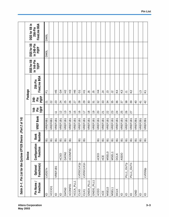
Pin List
IOLV
DS
7nB
1V
RE
F0B
121
F1
DM
0LD
M0L
VC
CIO
1B
1V
RE
F0B
122
IOV
RE
F1B
1B
1V
RE
F1B
111
23H
5
IOnC
SO
B1
VR
EF
1B1
1224
G4
DA
TA0
DA
TA0
B1
VR
EF
1B1
1325
H2
nCO
NF
IGnC
ON
FIG
B1
VR
EF
1B1
1426
H3
VC
CA
_PLL
1V
RE
F1B
115
27H
6
CLK
0LV
DS
CLK
1pB
1V
RE
F1B
116
28G
1
CLK
1LV
DS
CLK
1nB
1V
RE
F1B
117
29H
1
GN
DA
_PLL
1V
RE
F1B
118
30J6
GN
DG
_PLL
1V
RE
F1B
119
31J5
nCE
OnC
EO
B1
VR
EF
1B1
2032
H4
nCE
nCE
B1
VR
EF
1B1
2133
J4
MS
EL0
MS
EL0
B1
VR
EF
1B1
2234
J3
MS
EL1
MS
EL1
B1
VR
EF
1B1
2335
J2
DC
LKD
CLK
B1
VR
EF
1B1
2436
K4
IOA
SD
OB
1V
RE
F1B
125
37K
3
IOP
LL1_
OU
Tp
B1
VR
EF
1B1
2638
J1
IOP
LL1_
OU
Tn
B1
VR
EF
1B1
2739
K2
GN
DB
1V
RE
F2B
140
IOB
1V
RE
F2B
141
L3
IOLV
DS
6pB
1V
RE
F2B
142
K1
Tabl
e3–
1.Pi
n Li
st fo
r the
Cyc
lone
EP1
C6 D
evic
e (P
art2
of14
)
Devi
cePa
ckag
eDQ
S fo
r X8
in 1
44-P
inTQ
FP
DQS
for X
8 in
240
-Pin
PQFP
DQS
for X
8 in
25
6-Pi
nFi
neLi
neBG
APi
n Na
me
/ Fu
nctio
nOp
tiona
l Fu
nctio
n(s)
Conf
igur
atio
n Fu
nctio
nBa
nk
Num
ber
VREF
Ban
k14
4-Pi
nTQ
FP
240-
Pin
PQFP
256-
Pin
Fine
Line
BGA
Altera Corporation 3–3May 2003 Preliminary

Cyclone Device Handbook, Volume 2
IOLV
DS
6nB
1V
RE
F2B
143
L1
IOLV
DS
5pB
1V
RE
F2B
144
L2
IOLV
DS
5nB
1V
RE
F2B
145
M1
IOLV
DS
4pB
1V
RE
F2B
146
N1
IOLV
DS
4nB
1V
RE
F2B
147
M2
IOLV
DS
3pB
1V
RE
F2B
148
N2
DQ
0L4
DQ
0L4
IOLV
DS
3nB
1V
RE
F2B
149
M3
DQ
0L5
DQ
0L5
IOD
PC
LK0
B1
VR
EF
2B1
2850
L5D
QS
1L
VC
CIO
1B
1V
RE
F2B
129
51
GN
DB
1V
RE
F2B
130
52
IOLV
DS
2pB
1V
RE
F2B
153
M4
DQ
0L6
DQ
0L6
IOLV
DS
2nB
1V
RE
F2B
154
N3
DQ
0L7
DQ
0L7
IOV
RE
F2B
1B
1V
RE
F2B
131
55K
5
IOB
1V
RE
F2B
132
56L4
DQ
1L4
IOLV
DS
1pB
1V
RE
F2B
133
57R
1D
Q1L
5
IOLV
DS
1nB
1V
RE
F2B
134
58P
2D
Q1L
6
IOLV
DS
0pB
1V
RE
F2B
135
59P
3D
Q1L
7
IOLV
DS
0nB
1V
RE
F2B
136
60N
4
IOLV
DS
71p
B4
VR
EF
2B4
3761
R2
IOLV
DS
71n
B4
VR
EF
2B4
3862
T2
IOLV
DS
70p
B4
VR
EF
2B4
63R
3
IOLV
DS
70n
B4
VR
EF
2B4
64P
4
Tabl
e3–
1.Pi
n Li
st fo
r the
Cyc
lone
EP1
C6 D
evic
e (P
art3
of14
)
Devi
cePa
ckag
eDQ
S fo
r X8
in 1
44-P
inTQ
FP
DQS
for X
8 in
240
-Pin
PQFP
DQS
for X
8 in
25
6-Pi
nFi
neLi
neBG
APi
n Na
me
/ Fu
nctio
nOp
tiona
l Fu
nctio
n(s)
Conf
igur
atio
n Fu
nctio
nBa
nk
Num
ber
VREF
Ban
k14
4-Pi
nTQ
FP
240-
Pin
PQFP
256-
Pin
Fine
Line
BGA
3–4 Altera CorporationPreliminary May 2003

Pin List
IOLV
DS
69p
B4
VR
EF
2B4
3965
R4
DQ
1B7
IOLV
DS
69n
B4
VR
EF
2B4
4066
T4
DQ
1B6
IOLV
DS
68p
B4
VR
EF
2B4
4167
R5
DQ
1B5
DQ
1B7
DQ
1B7
IOLV
DS
68n
B4
VR
EF
2B4
4268
P5
DQ
1B4
DQ
1B6
DQ
1B6
GN
DB
4V
RE
F2B
443
69
VC
CIO
4B
4V
RE
F2B
444
70
GN
DV
RE
F2B
445
71
VC
CIN
TV
RE
F2B
446
72
IOD
PC
LK7
B4
VR
EF
2B4
4773
M5
DQ
S1B
DQ
S1B
DQ
S1B
IOV
RE
F2B
4B
4V
RE
F2B
448
74M
6
IOLV
DS
67p
B4
VR
EF
2B4
4975
N5
IOLV
DS
67n
B4
VR
EF
2B4
76N
6D
Q1B
5D
Q1B
5
IOLV
DS
66p
B4
VR
EF
2B4
77P
6D
Q1B
4D
Q1B
4
IOLV
DS
66n
B4
VR
EF
2B4
78R
6
IOB
4V
RE
F2B
479
M7
IOLV
DS
65p
B4
VR
EF
2B4
80T
6
IOLV
DS
65n
B4
VR
EF
2B4
81R
7
IOLV
DS
64p
B4
VR
EF
2B4
82P
7
IOLV
DS
64n
B4
VR
EF
2B4
83N
7
IOLV
DS
63p
B4
VR
EF
2B4
5084
R8
IOLV
DS
63n
B4
VR
EF
2B4
5185
T8
IOLV
DS
62p
B4
VR
EF
1B4
5286
N8
Tabl
e3–
1.Pi
n Li
st fo
r the
Cyc
lone
EP1
C6 D
evic
e (P
art4
of14
)
Devi
cePa
ckag
eDQ
S fo
r X8
in 1
44-P
inTQ
FP
DQS
for X
8 in
240
-Pin
PQFP
DQS
for X
8 in
25
6-Pi
nFi
neLi
neBG
APi
n Na
me
/ Fu
nctio
nOp
tiona
l Fu
nctio
n(s)
Conf
igur
atio
n Fu
nctio
nBa
nk
Num
ber
VREF
Ban
k14
4-Pi
nTQ
FP
240-
Pin
PQFP
256-
Pin
Fine
Line
BGA
Altera Corporation 3–5May 2003 Preliminary

Cyclone Device Handbook, Volume 2
IOLV
DS
62n
B4
VR
EF
1B4
5387
P8
IOB
4V
RE
F1B
488
M8
GN
DV
RE
F1B
454
89
VC
CIN
TV
RE
F1B
455
90
GN
DB
4V
RE
F1B
491
VC
CIO
4B
4V
RE
F1B
492
IOV
RE
F1B
4B
4V
RE
F1B
456
93M
10
IOLV
DS
61p
B4
VR
EF
1B4
5794
R9
DM
1BD
M1B
DM
1B
IOLV
DS
61n
B4
VR
EF
1B4
5895
T9
IOLV
DS
60p
B4
VR
EF
1B4
96P
9
IOLV
DS
60n
B4
VR
EF
1B4
97N
9
IOLV
DS
59p
B4
VR
EF
1B4
98R
10
IOLV
DS
59n
B4
VR
EF
1B4
5999
T11
IOLV
DS
58p
B4
VR
EF
1B4
100
N10
IOLV
DS
58n
B4
VR
EF
1B4
101
P10
IOLV
DS
57p
B4
VR
EF
0B4
102
R11
IOLV
DS
57n
B4
VR
EF
0B4
103
P11
IOLV
DS
56p
B4
VR
EF
0B4
104
N11
IOLV
DS
56n
B4
VR
EF
0B4
105
N12
IOB
4V
RE
F0B
460
106
M9
IOV
RE
F0B
4B
4V
RE
F0B
461
107
M11
IOD
PC
LK6
B4
VR
EF
0B4
6210
8M
12
Tabl
e3–
1.Pi
n Li
st fo
r the
Cyc
lone
EP1
C6 D
evic
e (P
art5
of14
)
Devi
cePa
ckag
eDQ
S fo
r X8
in 1
44-P
inTQ
FP
DQS
for X
8 in
240
-Pin
PQFP
DQS
for X
8 in
25
6-Pi
nFi
neLi
neBG
APi
n Na
me
/ Fu
nctio
nOp
tiona
l Fu
nctio
n(s)
Conf
igur
atio
n Fu
nctio
nBa
nk
Num
ber
VREF
Ban
k14
4-Pi
nTQ
FP
240-
Pin
PQFP
256-
Pin
Fine
Line
BGA
3–6 Altera CorporationPreliminary May 2003

Pin List
GN
DV
RE
F0B
463
109
VC
CIN
TV
RE
F0B
464
110
GN
DB
4V
RE
F0B
465
111
VC
CIO
4B
4V
RE
F0B
466
112
IOLV
DS
55p
B4
VR
EF
0B4
6711
3P
12D
Q1B
3D
Q1B
3D
Q1B
3
IOLV
DS
55n
B4
VR
EF
0B4
6811
4R
12D
Q1B
2D
Q1B
2D
Q1B
2
IOLV
DS
54p
B4
VR
EF
0B4
6911
5T
13D
Q1B
1D
Q1B
1D
Q1B
1
IOLV
DS
54n
B4
VR
EF
0B4
7011
6R
13D
Q1B
0D
Q1B
0D
Q1B
0
IOLV
DS
53p
B4
VR
EF
0B4
117
R14
IOLV
DS
53n
B4
VR
EF
0B4
118
P13
IOLV
DS
52p
B4
VR
EF
0B4
7111
9T
15
IOLV
DS
52n
B4
VR
EF
0B4
7212
0R
15
IOLV
DS
51n
B3
VR
EF
2B3
7312
1N
13
IOLV
DS
51p
B3
VR
EF
2B3
7412
2P
14
IOLV
DS
50n
B3
VR
EF
2B3
7512
3P
15
IOLV
DS
50p
B3
VR
EF
2B3
7612
4R
16
IOLV
DS
49n
B3
VR
EF
2B3
7712
5N
15D
Q1R
7D
Q1R
7D
Q1R
7
IOLV
DS
49p
B3
VR
EF
2B3
7812
6N
16D
Q1R
6
IOV
RE
F2B
3B
3V
RE
F2B
379
127
K12
IOB
3V
RE
F2B
312
8K
14D
Q1R
6D
Q1R
6
GN
DB
3V
RE
F2B
380
129
VC
CIO
3B
3V
RE
F2B
381
130
Tabl
e3–
1.Pi
n Li
st fo
r the
Cyc
lone
EP1
C6 D
evic
e (P
art6
of14
)
Devi
cePa
ckag
eDQ
S fo
r X8
in 1
44-P
inTQ
FP
DQS
for X
8 in
240
-Pin
PQFP
DQS
for X
8 in
25
6-Pi
nFi
neLi
neBG
APi
n Na
me
/ Fu
nctio
nOp
tiona
l Fu
nctio
n(s)
Conf
igur
atio
n Fu
nctio
nBa
nk
Num
ber
VREF
Ban
k14
4-Pi
nTQ
FP
240-
Pin
PQFP
256-
Pin
Fine
Line
BGA
Altera Corporation 3–7May 2003 Preliminary

Cyclone Device Handbook, Volume 2
IOD
PC
LK5
B3
VR
EF
2B3
8213
1L1
2D
QS
1RD
QS
1RD
QS
1R
IOLV
DS
48n
B3
VR
EF
2B3
8313
2N
14D
Q1R
5D
Q1R
5D
Q1R
5
IOLV
DS
48p
B3
VR
EF
2B3
8413
3M
13D
Q1R
4D
Q1R
4D
Q1R
4
IOLV
DS
47n
B3
VR
EF
2B3
8513
4M
14D
M1R
IOLV
DS
47p
B3
VR
EF
2B3
135
L13
IOLV
DS
46n
B3
VR
EF
2B3
136
M15
IOLV
DS
46p
B3
VR
EF
2B3
137
M16
IOLV
DS
45n
B3
VR
EF
2B3
138
L14
IOLV
DS
45p
B3
VR
EF
2B3
139
L15
IOLV
DS
44n
B3
VR
EF
2B3
140
L16
IOLV
DS
44p
B3
VR
EF
2B3
141
K16
GN
DB
3V
RE
F2B
314
2
IOP
LL2_
OU
Tn
B3
VR
EF
1B3
143
K15
IOP
LL2_
OU
Tp
B3
VR
EF
1B3
144
J16
CO
NF
_DO
NE
CO
NF
_DO
NE
B3
VR
EF
1B3
8614
5K
13
nSTA
TU
SnS
TAT
US
B3
VR
EF
1B3
8714
6J1
3
TC
KT
CK
B3
VR
EF
1B3
8814
7J1
4
TM
ST
MS
B3
VR
EF
1B3
8914
8J1
5
TD
OT
DO
B3
VR
EF
1B3
9014
9H
15
GN
DG
_PLL
2V
RE
F1B
391
150
J12
GN
DA
_PLL
2V
RE
F1B
315
1J1
1
CLK
3LV
DS
CLK
2nB
3V
RE
F1B
392
152
H16
Tabl
e3–
1.Pi
n Li
st fo
r the
Cyc
lone
EP1
C6 D
evic
e (P
art7
of14
)
Devi
cePa
ckag
eDQ
S fo
r X8
in 1
44-P
inTQ
FP
DQS
for X
8 in
240
-Pin
PQFP
DQS
for X
8 in
25
6-Pi
nFi
neLi
neBG
APi
n Na
me
/ Fu
nctio
nOp
tiona
l Fu
nctio
n(s)
Conf
igur
atio
n Fu
nctio
nBa
nk
Num
ber
VREF
Ban
k14
4-Pi
nTQ
FP
240-
Pin
PQFP
256-
Pin
Fine
Line
BGA
3–8 Altera CorporationPreliminary May 2003

Pin List
CLK
2LV
DS
CLK
2pB
3V
RE
F1B
393
153
G16
VC
CA
_PLL
2V
RE
F1B
394
154
H11
TD
IT
DI
B3
VR
EF
1B3
9515
5H
14
IOV
RE
F1B
3B
3V
RE
F1B
396
156
H12
VC
CIO
3B
3V
RE
F0B
315
7
IOLV
DS
43n
B3
VR
EF
0B3
158
G14
DM
1RD
M1R
IOLV
DS
43p
B3
VR
EF
0B3
159
G13
IOLV
DS
42n
B3
VR
EF
0B3
160
G15
IOLV
DS
42p
B3
VR
EF
0B3
161
F16
IOLV
DS
41n
B3
VR
EF
0B3
162
F14
IOLV
DS
41p
B3
VR
EF
0B3
163
F13
IOLV
DS
40n
B3
VR
EF
0B3
164
F15
IOLV
DS
40p
B3
VR
EF
0B3
165
E16
IOLV
DS
39n
B3
VR
EF
0B3
166
E15
IOLV
DS
39p
B3
VR
EF
0B3
9716
7D
16D
Q1R
3
IOLV
DS
38n
B3
VR
EF
0B3
9816
8D
15D
Q1R
2
IOLV
DS
38p
B3
VR
EF
0B3
9916
9E
14D
Q1R
1D
Q1R
3D
Q1R
3
IOD
PC
LK4
B3
VR
EF
0B3
100
170
F12
GN
DB
3V
RE
F0B
310
117
1
VC
CIO
3B
3V
RE
F0B
310
217
2
IOLV
DS
37n
B3
VR
EF
0B3
173
E13
DQ
1R2
DQ
1R2
IOLV
DS
37p
B3
VR
EF
0B3
174
D14
DQ
1R1
DQ
1R1
Tabl
e3–
1.Pi
n Li
st fo
r the
Cyc
lone
EP1
C6 D
evic
e (P
art8
of14
)
Devi
cePa
ckag
eDQ
S fo
r X8
in 1
44-P
inTQ
FP
DQS
for X
8 in
240
-Pin
PQFP
DQS
for X
8 in
25
6-Pi
nFi
neLi
neBG
APi
n Na
me
/ Fu
nctio
nOp
tiona
l Fu
nctio
n(s)
Conf
igur
atio
n Fu
nctio
nBa
nk
Num
ber
VREF
Ban
k14
4-Pi
nTQ
FP
240-
Pin
PQFP
256-
Pin
Fine
Line
BGA
Altera Corporation 3–9May 2003 Preliminary

Cyclone Device Handbook, Volume 2
IOB
3V
RE
F0B
310
317
5H
13D
Q1R
0D
Q1R
0D
Q1R
0
IOV
RE
F0B
3B
3V
RE
F0B
310
417
6G
12
IOLV
DS
36n
B3
VR
EF
0B3
105
177
B16
IOLV
DS
36p
B3
VR
EF
0B3
106
178
C15
IOLV
DS
35n
B3
VR
EF
0B3
107
179
C14
IOLV
DS
35p
B3
VR
EF
0B3
108
180
D13
IOLV
DS
34n
B2
VR
EF
0B2
109
181
B15
IOLV
DS
34p
B2
VR
EF
0B2
110
182
A15
IOLV
DS
33n
B2
VR
EF
0B2
183
B14
IOLV
DS
33p
B2
VR
EF
0B2
184
C13
IOLV
DS
32n
B2
VR
EF
0B2
111
185
B13
DQ
0T0
DQ
0T0
DQ
0T0
IOLV
DS
32p
B2
VR
EF
0B2
112
186
A13
DQ
0T1
DQ
0T1
DQ
0T1
IOLV
DS
31n
B2
VR
EF
0B2
113
187
B12
DQ
0T2
DQ
0T2
DQ
0T2
IOLV
DS
31p
B2
VR
EF
0B2
114
188
C12
DQ
0T3
DQ
0T3
DQ
0T3
VC
CIO
2B
2V
RE
F0B
211
518
9
GN
DB
2V
RE
F0B
211
619
0
VC
CIN
TV
RE
F0B
211
719
1
GN
DV
RE
F0B
211
819
2
IOD
PC
LK3
B2
VR
EF
0B2
119
193
E12
DQ
S0T
DQ
S0T
DQ
S0T
IOV
RE
F0B
2B
2V
RE
F0B
212
019
4E
11
IOB
2V
RE
F0B
212
119
5E
9
IOLV
DS
30n
B2
VR
EF
0B2
196
D12
Tabl
e3–
1.Pi
n Li
st fo
r the
Cyc
lone
EP1
C6 D
evic
e (P
art9
of14
)
Devi
cePa
ckag
eDQ
S fo
r X8
in 1
44-P
inTQ
FP
DQS
for X
8 in
240
-Pin
PQFP
DQS
for X
8 in
25
6-Pi
nFi
neLi
neBG
APi
n Na
me
/ Fu
nctio
nOp
tiona
l Fu
nctio
n(s)
Conf
igur
atio
n Fu
nctio
nBa
nk
Num
ber
VREF
Ban
k14
4-Pi
nTQ
FP
240-
Pin
PQFP
256-
Pin
Fine
Line
BGA
3–10 Altera CorporationPreliminary May 2003
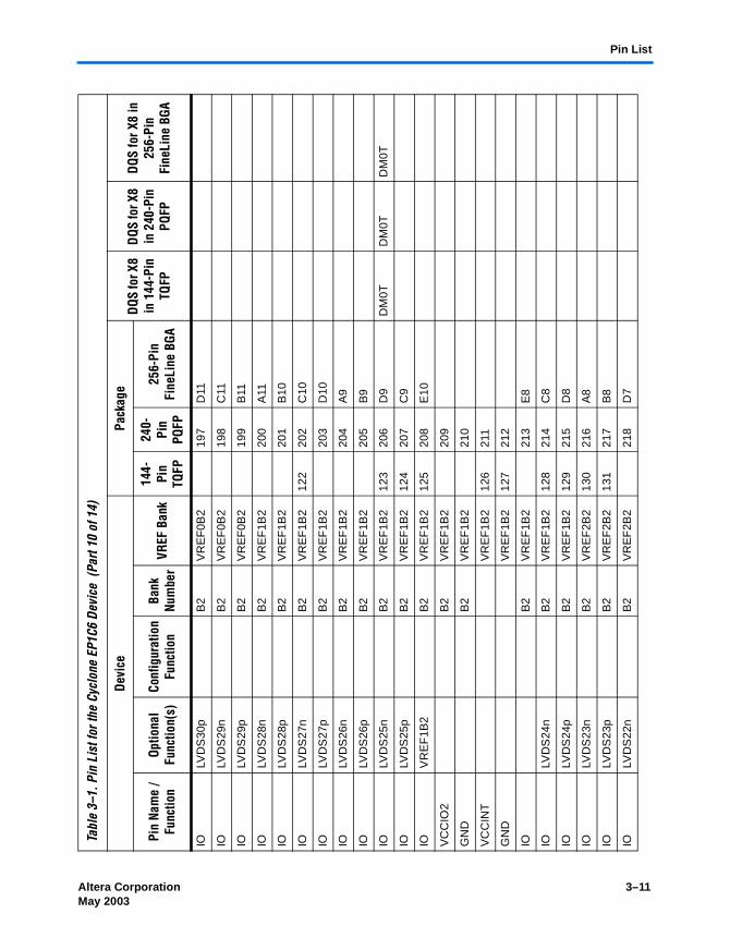
Pin List
IOLV
DS
30p
B2
VR
EF
0B2
197
D11
IOLV
DS
29n
B2
VR
EF
0B2
198
C11
IOLV
DS
29p
B2
VR
EF
0B2
199
B11
IOLV
DS
28n
B2
VR
EF
1B2
200
A11
IOLV
DS
28p
B2
VR
EF
1B2
201
B10
IOLV
DS
27n
B2
VR
EF
1B2
122
202
C10
IOLV
DS
27p
B2
VR
EF
1B2
203
D10
IOLV
DS
26n
B2
VR
EF
1B2
204
A9
IOLV
DS
26p
B2
VR
EF
1B2
205
B9
IOLV
DS
25n
B2
VR
EF
1B2
123
206
D9
DM
0TD
M0T
DM
0T
IOLV
DS
25p
B2
VR
EF
1B2
124
207
C9
IOV
RE
F1B
2B
2V
RE
F1B
212
520
8E
10
VC
CIO
2B
2V
RE
F1B
220
9
GN
DB
2V
RE
F1B
221
0
VC
CIN
TV
RE
F1B
212
621
1
GN
DV
RE
F1B
212
721
2
IOB
2V
RE
F1B
221
3E
8
IOLV
DS
24n
B2
VR
EF
1B2
128
214
C8
IOLV
DS
24p
B2
VR
EF
1B2
129
215
D8
IOLV
DS
23n
B2
VR
EF
2B2
130
216
A8
IOLV
DS
23p
B2
VR
EF
2B2
131
217
B8
IOLV
DS
22n
B2
VR
EF
2B2
218
D7
Tabl
e3–
1.Pi
n Li
st fo
r the
Cyc
lone
EP1
C6 D
evic
e (P
art1
0of
14)
Devi
cePa
ckag
eDQ
S fo
r X8
in 1
44-P
inTQ
FP
DQS
for X
8 in
240
-Pin
PQFP
DQS
for X
8 in
25
6-Pi
nFi
neLi
neBG
APi
n Na
me
/ Fu
nctio
nOp
tiona
l Fu
nctio
n(s)
Conf
igur
atio
n Fu
nctio
nBa
nk
Num
ber
VREF
Ban
k14
4-Pi
nTQ
FP
240-
Pin
PQFP
256-
Pin
Fine
Line
BGA
Altera Corporation 3–11May 2003 Preliminary

Cyclone Device Handbook, Volume 2
IOLV
DS
22p
B2
VR
EF
2B2
219
C7
IOLV
DS
21n
B2
VR
EF
2B2
220
B7
IOLV
DS
21p
B2
VR
EF
2B2
221
A6
IOB
2V
RE
F2B
222
2E
7
IOLV
DS
20n
B2
VR
EF
2B2
223
B6
IOLV
DS
20p
B2
VR
EF
2B2
224
C6
IOLV
DS
19n
B2
VR
EF
2B2
225
D6
IOLV
DS
19p
B2
VR
EF
2B2
132
226
D5
IOV
RE
F2B
2B
2V
RE
F2B
213
322
7E
6
IOD
PC
LK2
B2
VR
EF
2B2
134
228
E5
VC
CIN
TV
RE
F2B
213
522
9
GN
DV
RE
F2B
213
623
0
VC
CIO
2B
2V
RE
F2B
213
723
1
GN
DB
2V
RE
F2B
213
823
2
IOLV
DS
18n
B2
VR
EF
2B2
139
233
C5
DQ
0T4
DQ
0T4
DQ
0T4
IOLV
DS
18p
B2
VR
EF
2B2
140
234
B5
DQ
0T5
DQ
0T5
DQ
0T5
IOLV
DS
17n
B2
VR
EF
2B2
141
235
A4
DQ
0T6
DQ
0T6
DQ
0T6
IOLV
DS
17p
B2
VR
EF
2B2
142
236
B4
DQ
0T7
DQ
0T7
DQ
0T7
IOLV
DS
16n
B2
VR
EF
2B2
237
C4
IOLV
DS
16p
B2
VR
EF
2B2
238
B3
IOLV
DS
15n
DE
V_O
EB
2V
RE
F2B
214
323
9A
2
IOLV
DS
15p
DE
V_C
LRn
B2
VR
EF
2B2
144
240
B2
Tabl
e3–
1.Pi
n Li
st fo
r the
Cyc
lone
EP1
C6 D
evic
e (P
art1
1of
14)
Devi
cePa
ckag
eDQ
S fo
r X8
in 1
44-P
inTQ
FP
DQS
for X
8 in
240
-Pin
PQFP
DQS
for X
8 in
25
6-Pi
nFi
neLi
neBG
APi
n Na
me
/ Fu
nctio
nOp
tiona
l Fu
nctio
n(s)
Conf
igur
atio
n Fu
nctio
nBa
nk
Num
ber
VREF
Ban
k14
4-Pi
nTQ
FP
240-
Pin
PQFP
256-
Pin
Fine
Line
BGA
3–12 Altera CorporationPreliminary May 2003

Pin List
VC
CIN
TA
7
VC
CIN
TA
10
VC
CIN
TG
8
VC
CIN
TG
10
VC
CIN
TH
7
VC
CIN
TH
9
VC
CIN
TJ8
VC
CIN
TJ1
0
VC
CIN
TK
7
VC
CIN
TK
9
VC
CIN
TT
7
VC
CIN
TT
10
VC
CIO
1C
1
VC
CIO
1G
6
VC
CIO
1P
1
VC
CIO
4T
3
VC
CIO
4L7
VC
CIO
4L1
0
VC
CIO
4T
14
VC
CIO
3P
16
VC
CIO
3K
11
VC
CIO
3C
16
Tabl
e3–
1.Pi
n Li
st fo
r the
Cyc
lone
EP1
C6 D
evic
e (P
art1
2of
14)
Devi
cePa
ckag
eDQ
S fo
r X8
in 1
44-P
inTQ
FP
DQS
for X
8 in
240
-Pin
PQFP
DQS
for X
8 in
25
6-Pi
nFi
neLi
neBG
APi
n Na
me
/ Fu
nctio
nOp
tiona
l Fu
nctio
n(s)
Conf
igur
atio
n Fu
nctio
nBa
nk
Num
ber
VREF
Ban
k14
4-Pi
nTQ
FP
240-
Pin
PQFP
256-
Pin
Fine
Line
BGA
Altera Corporation 3–13May 2003 Preliminary

Cyclone Device Handbook, Volume 2
VC
CIO
2A
14
VC
CIO
2F
10
VC
CIO
2F
7
VC
CIO
2A
3
GN
DA
1
GN
DA
16
GN
DA
5
GN
DA
12
GN
DF
6
GN
DF
8
GN
DF
9
GN
DF
11
GN
DG
7
GN
DG
9
GN
DG
11
GN
DH
8
GN
DH
10
GN
DJ7
GN
DJ9
GN
DK
6
GN
DK
8
GN
DK
10
Tabl
e3–
1.Pi
n Li
st fo
r the
Cyc
lone
EP1
C6 D
evic
e (P
art1
3of
14)
Devi
cePa
ckag
eDQ
S fo
r X8
in 1
44-P
inTQ
FP
DQS
for X
8 in
240
-Pin
PQFP
DQS
for X
8 in
25
6-Pi
nFi
neLi
neBG
APi
n Na
me
/ Fu
nctio
nOp
tiona
l Fu
nctio
n(s)
Conf
igur
atio
n Fu
nctio
nBa
nk
Num
ber
VREF
Ban
k14
4-Pi
nTQ
FP
240-
Pin
PQFP
256-
Pin
Fine
Line
BGA
3–14 Altera CorporationPreliminary May 2003
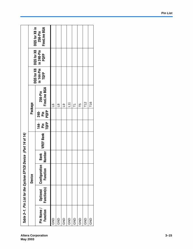
Pin List
GN
DL6
GN
DL8
GN
DL9
GN
DL1
1
GN
DT
1
GN
DT
5
GN
DT
12
GN
DT
16
Tabl
e3–
1.Pi
n Li
st fo
r the
Cyc
lone
EP1
C6 D
evic
e (P
art1
4of
14)
Devi
cePa
ckag
eDQ
S fo
r X8
in 1
44-P
inTQ
FP
DQS
for X
8 in
240
-Pin
PQFP
DQS
for X
8 in
25
6-Pi
nFi
neLi
neBG
APi
n Na
me
/ Fu
nctio
nOp
tiona
l Fu
nctio
n(s)
Conf
igur
atio
n Fu
nctio
nBa
nk
Num
ber
VREF
Ban
k14
4-Pi
nTQ
FP
240-
Pin
PQFP
256-
Pin
Fine
Line
BGA
Altera Corporation 3–15May 2003 Preliminary

Cyclone Device Handbook, Volume 2
Pin
Defin
ition
sTa
ble
3–2
show
s p
in d
efin
itio
ns fo
r th
e E
P1C
6 d
evic
e.
Tabl
e3–
2.Pi
n De
finiti
ons
for t
he E
P1C6
Dev
ice
(Pa
rt1
of4)
Pin
Nam
ePi
n Ty
pe (1
st, 2
nd, &
3rd
Fun
ctio
n)Pi
n De
scrip
tion
Supp
ly a
nd R
efer
ence
Pin
s
VC
CIO
[1..4
]P
ower
The
se a
re I/
O s
uppl
y vo
ltage
pin
s fo
r ba
nks
1 th
roug
h 4.
Eac
h ba
nk c
an s
uppo
rt
a di
ffere
nt v
olta
ge le
vel.
VC
CIO
sup
plie
s po
wer
to th
e ou
tput
buf
fers
for
all I
/O
stan
dard
s. V
CC
IO a
lso
supp
lies
pow
er to
the
inpu
t buf
fers
use
d fo
r th
e LV
TT
L,
LVC
MO
S, 1
.5-V
, 1.8
-V, 2
.5-V
, and
3.3
-V P
CI I
/O s
tand
ards
.
VC
CIN
TP
ower
The
se a
re in
tern
al lo
gic
arra
y vo
ltage
sup
ply
pins
. VC
CIN
T a
lso
supp
lies
pow
er to
th
e in
put b
uffe
rs u
sed
for
the
LVD
S, S
ST
L2, a
nd S
ST
L3 I/
O s
tand
ards
.
VR
EF
[0..2
]B[1
..4]
I/O, I
nput
Inpu
t ref
eren
ce v
olta
ge fo
r ba
nks
1-4.
If a
ban
k us
es a
vol
tage
-ref
eren
ced
I/O
stan
dard
, the
n th
ese
pins
are
use
d as
the
volta
ge-r
efer
ence
pin
s fo
r th
e ba
nk. I
f vo
ltage
ref
eren
ce I/
O s
tand
ards
are
not
use
d in
the
bank
, the
VR
EF
pin
s ar
e av
aila
ble
as u
ser
I/O p
ins.
VC
CA
_PLL
[1..2
]P
ower
Ana
log
pow
er fo
r P
LLs[
1..2
]. T
he d
esig
ner
mus
t con
nect
this
pin
to 1
.5 V
, eve
n if
the
PLL
is n
ot u
sed.
GN
DA
_PLL
[1..2
]G
roun
dA
nalo
g gr
ound
for P
LLs[
1..2
]. T
he d
esig
ner c
an c
onne
ct th
is p
in to
the
GN
D p
lane
on
the
boar
d.
GN
DG
_PLL
[1..2
]G
roun
dG
uard
rin
g gr
ound
for
PLL
s[1.
.2].
The
des
igne
r ca
n co
nnec
t thi
s pi
n to
the
GN
D
plan
e on
the
boar
d.
Conf
igur
atio
n an
d JT
AG P
ins
CO
NF
_DO
NE
Bid
irect
iona
l (op
en-d
rain
)T
his
is a
ded
icat
ed c
onfig
urat
ion
stat
us p
in; i
t is
not a
vaila
ble
as a
use
r I/O
pin
.
nSTA
TU
SB
idire
ctio
nal (
open
-dra
in)
Thi
s is
a d
edic
ated
con
figur
atio
n st
atus
pin
; it i
s no
t ava
ilabl
e as
a u
ser
I/O p
in.
nCO
NF
IGIn
put
Ded
icat
ed c
onfig
urat
ion
cont
rol i
nput
. A lo
w tr
ansi
tion
rese
ts th
e ta
rget
dev
ice;
a
low
-to-
high
tran
sitio
n be
gins
con
figur
atio
n. A
ll I/O
pin
s tr
i-sta
te w
hen
nCO
NF
IG is
dr
iven
low
.
DC
LKIn
put (
PS
mod
e), O
utpu
t (A
S m
ode)
In p
assi
ve s
eria
l con
figur
atio
n m
ode,
DC
LK is
a c
lock
inpu
t use
d to
clo
ck
conf
igur
atio
n da
ta fr
om a
n ex
tern
al s
ourc
e in
to th
e C
yclo
ne d
evic
e. In
act
ive
seria
l co
nfig
urat
ion
mod
e, D
CLK
is a
clo
ck o
utpu
t fro
m th
e C
yclo
ne d
evic
e (t
he C
yclo
ne
devi
ce a
cts
as m
aste
r in
this
mod
e). T
his
is a
ded
icat
ed p
in u
sed
for c
onfig
urat
ion.
3–16 Altera CorporationPreliminary May 2003

Pin Definitions
DA
TA0
Inpu
tD
edic
ated
con
figur
atio
n da
ta in
put p
in.
nCE
Inpu
tA
ctiv
e-lo
w c
hip
enab
le. D
edic
ated
chi
p en
able
inpu
t use
d to
det
ect w
hich
dev
ice
is a
ctiv
e in
a c
hain
of d
evic
es. W
hen
nCE
is lo
w, t
he d
evic
e is
ena
bled
. Whe
n nC
E
is h
igh,
the
devi
ce is
dis
able
d.
nCE
OO
utpu
tO
utpu
t tha
t driv
es lo
w w
hen
devi
ce c
onfig
urat
ion
is c
ompl
ete.
Dur
ing
mul
ti-de
vice
co
nfig
urat
ion,
this
pin
feed
s a
subs
eque
nt d
evic
e’s
nCE
pin
.
AS
DO
I/O, O
utpu
tA
ctiv
e se
rial d
ata
outp
ut fr
om th
e C
yclo
ne d
evic
e. T
his
outp
ut p
in is
util
ized
dur
ing
activ
e se
rial c
onfig
urat
ion
mod
e. T
he C
yclo
ne d
evic
e co
ntro
ls c
onfig
urat
ion
and
driv
es a
ddre
ss a
nd c
ontr
ol in
form
atio
n ou
t on
AS
DO
. In
pass
ive
seria
l co
nfig
urat
ion,
this
pin
is a
vaila
ble
as a
use
r I/O
pin
.
nCS
OI/O
, Out
put
Chi
p se
lect
out
put t
hat e
nabl
es/d
isab
les
a se
rial c
onfig
urat
ion
devi
ce.
Thi
s ou
tput
is
util
ized
dur
ing
activ
e se
rial c
onfig
urat
ion
mod
e. T
he C
yclo
ne d
evic
e co
ntro
ls
conf
igur
atio
n an
d en
able
s th
e se
rial c
onfig
urat
ion
devi
ce b
y dr
ivin
g nC
SO
low
. In
pass
ive
seria
l con
figur
atio
n, th
is p
in is
ava
ilabl
e as
a u
ser
I/O p
in.
INIT
_DO
NE
I/O, O
utpu
t (op
en-d
rain
)T
his
is a
dua
l-pur
pose
pin
and
can
be
used
as
an I/
O p
in w
hen
not e
nabl
ed a
s IN
IT_D
ON
E. W
hen
enab
led,
the
pin
indi
cate
s w
hen
the
devi
ce h
as e
nter
ed u
ser
mod
e. T
his
pin
can
be u
sed
as a
use
r I/O
pin
afte
r co
nfig
urat
ion.
CLK
US
RI/O
, Inp
utO
ptio
nal u
ser-
supp
lied
cloc
k in
put.
Syn
chro
nize
s th
e in
itial
izat
ion
of o
ne o
r m
ore
devi
ces.
Thi
s pi
n ca
n be
use
d as
a u
ser
I/O p
in a
fter
conf
igur
atio
n.
DE
V_C
LRn
I/O, I
nput
Dua
l-pur
pose
pin
that
can
ove
rrid
e al
l cle
ars
on a
ll de
vice
regi
ster
s. W
hen
this
pin
is
driv
en lo
w, a
ll re
gist
ers
are
clea
red;
whe
n th
is p
in is
driv
en h
igh,
all
regi
ster
s be
have
as
defin
ed in
the
desi
gn.
DE
V_O
EI/O
, Inp
utD
ual-p
urpo
se p
in th
at c
an o
verr
ide
all t
ri-st
ates
on
the
devi
ce. W
hen
this
pin
is
driv
en lo
w, a
ll I/O
pin
s ar
e tr
i-sta
ted;
whe
n th
is p
in is
driv
en h
igh,
all
I/O p
ins
beha
ve a
s de
fined
in th
e de
sign
.
MS
EL[
1..0
]In
put
Ded
icat
ed m
ode
sele
ct c
ontr
ol p
ins
that
set
the
conf
igur
atio
n m
ode
for t
he d
evic
e.
TM
SIn
put
Thi
s is
a d
edic
ated
JTA
G in
put p
in.
TD
IIn
put
Thi
s is
a d
edic
ated
JTA
G in
put p
in.
TC
KIn
put
Thi
s is
a d
edic
ated
JTA
G in
put p
in.
TD
OO
utpu
tT
his
is a
ded
icat
ed J
TAG
out
put p
in.
Tabl
e3–
2.Pi
n De
finiti
ons
for t
he E
P1C6
Dev
ice
(Pa
rt2
of4)
Pin
Nam
ePi
n Ty
pe (1
st, 2
nd, &
3rd
Fun
ctio
n)Pi
n De
scrip
tion
Altera Corporation 3–17May 2003 Preliminary

Cyclone Device Handbook, Volume 2
Cloc
k an
d PL
L Pi
ns
CLK
0In
put,
LVD
S In
put
Ded
icat
ed g
loba
l clo
ck in
put.
The
dua
l-fun
ctio
n of
CLK
0 is
LV
DS
CLK
1p, w
hich
is
used
for
diffe
rent
ial i
nput
to P
LL1.
CLK
1In
put,
LVD
S In
put
Ded
icat
ed g
loba
l clo
ck in
put.
The
dua
l-fun
ctio
n of
CLK
1 is
LV
DS
CLK
1n, w
hich
is
used
for
diffe
rent
ial i
nput
to P
LL1.
CLK
2In
put,
LVD
S In
put
Ded
icat
ed g
loba
l clo
ck in
put.
The
dua
l-fun
ctio
n of
CLK
2 is
LV
DS
CLK
2p, w
hich
is
used
for
diffe
rent
ial i
nput
to P
LL2.
CLK
3In
put,
LVD
S In
put
Ded
icat
ed g
loba
l clo
ck in
put.
The
dua
l-fun
ctio
n of
CLK
3 is
LV
DS
CLK
2n, w
hich
is
used
for
diffe
rent
ial i
nput
to P
LL2.
DP
CLK
[7..0
]I/O
Dua
l-pur
pose
clo
ck p
ins
that
can
con
nect
to th
e gl
obal
clo
ck n
etw
ork.
The
se p
ins
can
be u
sed
for
high
fan-
out c
ontr
ol s
igna
ls, s
uch
as c
lock
s, c
lear
s, IR
DY,
TR
DY,
or
DQ
S s
igna
ls.
The
se p
ins
are
also
ava
ilabl
e as
use
r I/O
pin
s.
PLL
1_O
UT
pI/O
, Out
put
Ext
erna
l clo
ck o
utpu
t fro
m P
LL 1
. Thi
s pi
n ca
n be
use
d w
ith d
iffer
entia
l or
sing
le
ende
d I/O
sta
ndar
ds. I
f clo
ck o
utpu
t fro
m P
LL1
is n
ot u
sed,
this
pin
is a
vaila
ble
as
a us
er I/
O p
in.
PLL
1_O
UT
nI/O
, Out
put
Neg
ativ
e te
rmin
al fo
r ex
tern
al c
lock
out
put f
rom
PLL
1. If
the
cloc
k ou
tput
is s
ingl
e en
ded,
this
pin
is a
vaila
ble
as a
use
r I/O
pin
.
PLL
2_O
UT
pI/O
, Out
put
Ext
erna
l clo
ck o
utpu
t fro
m P
LL 2
. Thi
s pi
n ca
n be
use
d w
ith d
iffer
entia
l or
sing
le
ende
d I/O
sta
ndar
ds. I
f clo
ck o
utpu
t fro
m P
LL2
is n
ot u
sed,
this
pin
is a
vaila
ble
as
a us
er I/
O p
in. T
he E
P1C
6T14
4 do
es n
ot s
uppo
rt th
is o
utpu
t pin
.
PLL
2_O
UT
nI/O
, Out
put
Neg
ativ
e te
rmin
al fo
r ex
tern
al c
lock
out
put f
rom
PLL
2. If
the
cloc
k ou
tput
is s
ingl
e en
ded,
this
pin
is a
vaila
ble
as a
use
r I/O
pin
. The
EP
1C6T
144
does
not
sup
port
th
is o
utpu
t pin
.
Dual
-Pur
pose
LVD
S &
Ext
erna
l Mem
ory
Inte
rface
Pin
s
LVD
S[0
..71]
pI/O
, LV
DS
RX
or
TX
Dua
l-pur
pose
LV
DS
I/O
cha
nnel
s 0
to 7
1. T
hese
cha
nnel
s ca
n be
use
d fo
r re
ceiv
ing
or tr
ansm
ittin
g LV
DS
com
patib
le s
igna
ls. P
ins
with
a "
p" s
uffix
car
ry th
e po
sitiv
e si
gnal
for
the
diffe
rent
ial c
hann
el. I
f not
use
d fo
r LV
DS
inte
rfac
ing,
thes
e pi
ns a
re a
vaila
ble
as u
ser
I/O p
ins.
Tabl
e3–
2.Pi
n De
finiti
ons
for t
he E
P1C6
Dev
ice
(Pa
rt3
of4)
Pin
Nam
ePi
n Ty
pe (1
st, 2
nd, &
3rd
Fun
ctio
n)Pi
n De
scrip
tion
3–18 Altera CorporationPreliminary May 2003

Pin Definitions
LVD
S[0
..71]
nI/O
, LV
DS
RX
or
TX
Dua
l-pur
pose
LV
DS
I/O
cha
nnel
s 0
to 7
1. T
hese
cha
nnel
s ca
n be
use
d fo
r re
ceiv
ing
or tr
ansm
ittin
g LV
DS
com
patib
le s
igna
ls. P
ins
with
an
"n"
suffi
x ca
rry
the
nega
tive
sign
al fo
r th
e di
ffere
ntia
l cha
nnel
. If n
ot u
sed
for L
VD
S in
terf
acin
g, th
ese
pins
are
ava
ilabl
e as
use
r I/O
pin
s.
LVD
SC
LK1p
Inpu
t, LV
DS
Inpu
tD
ual-p
urpo
se L
VD
S c
lock
inpu
t to
PLL
1. I
f diff
eren
tial i
nput
to P
LL1
is n
ot
requ
ired,
this
pin
is a
vaila
ble
as th
e C
LK0
inpu
t pin
.
LVD
SC
LK1n
Inpu
t, LV
DS
Inpu
tD
ual-p
urpo
se L
VD
S c
lock
inpu
t to
PLL
1. I
f diff
eren
tial i
nput
to P
LL1
is n
ot
requ
ired,
this
pin
is a
vaila
ble
as th
e C
LK1
inpu
t pin
.
LVD
SC
LK2p
Inpu
t, LV
DS
Inpu
tD
ual-p
urpo
se L
VD
S c
lock
inpu
t to
PLL
2. I
f diff
eren
tial i
nput
to P
LL2
is n
ot
requ
ired,
this
pin
is a
vaila
ble
as th
e C
LK2
inpu
t pin
.
LVD
SC
LK2n
Inpu
t, LV
DS
Inpu
tD
ual-p
urpo
se L
VD
S c
lock
inpu
t to
PLL
2. I
f diff
eren
tial i
nput
to P
LL2
is n
ot
requ
ired,
this
pin
is a
vaila
ble
as th
e C
LK3
inpu
t pin
.
DQ
S[0
..1][L
,R,T
,B]
I/OO
ptio
nal d
ata
stro
be s
igna
l for
use
in e
xter
nal m
emor
y in
terf
acin
g. T
hese
pin
s al
so
func
tion
as D
PC
LK p
ins;
ther
efor
e, th
e D
QS
sig
nals
can
con
nect
to th
e gl
obal
cl
ock
netw
ork.
A p
rogr
amm
able
del
ay c
hain
is u
sed
to s
hift
the
DQ
S s
igna
ls b
y 90
or
72
degr
ees.
DQ
[0..7
][L,R
,T,B
]I/O
Opt
iona
l dat
a si
gnal
for
use
in e
xter
nal m
emor
y in
terf
acin
g.
DM
[0..1
][L,R
,T,B
]I/O
Opt
iona
l dat
a m
ask
outp
ut s
igna
l for
use
in e
xter
nal m
emor
y in
terf
acin
g.
Tabl
e3–
2.Pi
n De
finiti
ons
for t
he E
P1C6
Dev
ice
(Pa
rt4
of4)
Pin
Nam
ePi
n Ty
pe (1
st, 2
nd, &
3rd
Fun
ctio
n)Pi
n De
scrip
tion
Altera Corporation 3–19May 2003 Preliminary

Cyclone Device Handbook, Volume 2
PLL & Bank Diagram
Figure shows the PLL and Bank locations for the EP1C6 device.
Figure 3–1. PLL and Bank Diagram (1), (2)
Notes for Figure:(1) This is a top view of the silicon die. (2) This is a pictoral representation only to get an idea of placement on the device. Refer to the pin-list and
B2
VR
EF
0B1
B1
VR
EF
1B1
PLL1 PLL2
VR
EB
2B1
VREF2B2 VREF1B2 VREF0B2
VR
EB
2B3
B4VREF2B4 VREF1B4 VREF0B4
B3
VR
EF
0B3
VR
EF
1B3
3–20 Altera CorporationPreliminary May 2003

Altera Corporation May 2003
C52004-1.0
4. Cyclone EP1C12 DevicePin Information
Introduction The following tables contain pin information for the Cyclone EP1C12 device, organized into the following sections:
Section Page
Pin List. . . . . . . . . . . . . . . . . . . . . . . . . . . . . . . . . . . . . . . . . . . . . . 4–2Pin Definitions . . . . . . . . . . . . . . . . . . . . . . . . . . . . . . . . . . . . . . 4–20PLL & Bank Diagram . . . . . . . . . . . . . . . . . . . . . . . . . . . . . . . . 4–24
4–1Preliminary

Cyclone Device Handbook, Volume 2
Pin
List
Tabl
e4–
1 sh
ows
the
com
ple
te p
in li
st fo
r th
e d
evic
e C
yclo
ne E
P1C
12 d
evic
e:
Tabl
e4–
1.Pi
n Li
st fo
r the
Cyc
lone
EP1
C12
Devi
ce (
Part
1of
18)
Dev
ice
Pack
age
DQS
for
X8 in
24
0-Pi
n PQ
FP
DQS
for X
8 in
25
6-Pi
n Fi
neLi
neBG
A
DQS
for X
8 in
32
4-Pi
n Fi
neLi
neBG
APi
n N
ame
/ Fu
nctio
nOp
tiona
l Fu
nctio
n(s)
Conf
igur
atio
n Fu
nctio
nBa
nk
Num
.VR
EF
Bank
240-
Pin
PQFP
256-
Pin
Fine
Line
BGA
324-
Pin
Fine
Line
BGA
IOLV
DS
23p
INIT
_DO
NE
B1
VR
EF
0B1
1D
4C
3
IOLV
DS
23n
B1
VR
EF
0B1
2C
3C
2
IOLV
DS
22p
CLK
US
RB
1V
RE
F0B
13
C2
D3
IOLV
DS
22n
B1
VR
EF
0B1
4B
1D
2
IOV
RE
F0B
1B
1V
RE
F0B
15
G5
D4
IOB
1V
RE
F0B
16
F4
D1
IOLV
DS
21p
B1
VR
EF
0B1
7D
3E
3D
Q0L
0D
Q0L
0D
Q0L
0
IOLV
DS
21n
B1
VR
EF
0B1
8E
4E
2D
Q0L
1D
Q0L
1D
Q0L
1
VC
CIO
1B
1V
RE
F0B
19
GN
DB
1V
RE
F0B
110
IOD
PC
LK1
B1
VR
EF
0B1
11F
5F
1D
QS
0LD
QS
0LD
QS
0L
IOLV
DS
20p
B1
VR
EF
0B1
12E
3E
4D
Q0L
2D
Q0L
2D
Q0L
2
IOLV
DS
20n
B1
VR
EF
0B1
13D
2E
5D
Q0L
3D
Q0L
3D
Q0L
3
IOLV
DS
19p
B1
VR
EF
0B1
14E
2F
2
IOLV
DS
19n
B1
VR
EF
0B1
15D
1F
3
IOLV
DS
18p
B1
VR
EF
0B1
16F
3F
4
IOLV
DS
18n
B1
VR
EF
0B1
17G
3F
5
IOLV
DS
17p
B1
VR
EF
0B1
18F
2G
1
IOLV
DS
17n
B1
VR
EF
0B1
19E
1G
2
IOLV
DS
16p
B1
VR
EF
0B1
20G
2F
6
4–2 Altera CorporationPreliminary May 2003

Pin List
IOLV
DS
16n
B1
VR
EF
0B1
21F
1F
7D
M0L
DM
0L
IOLV
DS
15p
B1
VR
EF
0B1
G3
IOLV
DS
15n
B1
VR
EF
0B1
G4
DQ
0L4
IOLV
DS
14p
B1
VR
EF
0B1
G5
DQ
0L5
IOLV
DS
14n
B1
VR
EF
0B1
G6
DQ
0L6
IOB
1V
RE
F0B
1H
1D
Q0L
7
VC
CIO
1B
1V
RE
F0B
122
GN
DB
1V
RE
F0B
1
IOLV
DS
13p
B1
VR
EF
1B1
H2
IOLV
DS
13n
B1
VR
EF
1B1
H3
IOLV
DS
12p
B1
VR
EF
1B1
H4
IOLV
DS
12n
B1
VR
EF
1B1
H5
DM
0L
IOV
RE
F1B
1B
1V
RE
F1B
123
H5
H6
IOnC
SO
B1
VR
EF
1B1
24G
4J1
DA
TA0
DA
TA0
B1
VR
EF
1B1
25H
2H
7
nCO
NF
IGnC
ON
FIG
B1
VR
EF
1B1
26H
3J2
VC
CA
_PLL
1V
RE
F1B
127
H6
J5
CLK
0LV
DS
CLK
1pB
1V
RE
F1B
128
G1
J3
CLK
1LV
DS
CLK
1nB
1V
RE
F1B
129
H1
J4
GN
DA
_PLL
1V
RE
F1B
130
J6K
1
GN
DG
_PLL
1V
RE
F1B
131
J5J6
nCE
OnC
EO
B1
VR
EF
1B1
32H
4K
2
Tabl
e4–
1.Pi
n Li
st fo
r the
Cyc
lone
EP1
C12
Devi
ce (
Part
2of
18)
Dev
ice
Pack
age
DQS
for
X8 in
24
0-Pi
n PQ
FP
DQS
for X
8 in
25
6-Pi
n Fi
neLi
neBG
A
DQS
for X
8 in
32
4-Pi
n Fi
neLi
neBG
APi
n N
ame
/ Fu
nctio
nOp
tiona
l Fu
nctio
n(s)
Conf
igur
atio
n Fu
nctio
nBa
nk
Num
.VR
EF
Bank
240-
Pin
PQFP
256-
Pin
Fine
Line
BGA
324-
Pin
Fine
Line
BGA
Altera Corporation 4–3May 2003 Preliminary

Cyclone Device Handbook, Volume 2
nCE
nCE
B1
VR
EF
1B1
33J4
J7
MS
EL0
MS
EL0
B1
VR
EF
1B1
34J3
K3
MS
EL1
MS
EL1
B1
VR
EF
1B1
35J2
K7
DC
LKD
CLK
B1
VR
EF
1B1
36K
4L1
IOA
SD
OB
1V
RE
F1B
137
K3
K6
IOP
LL1_
OU
Tp
B1
VR
EF
1B1
38J1
K4
IOP
LL1_
OU
Tn
B1
VR
EF
1B1
39K
2K
5
IOLV
DS
11p
B1
VR
EF
1B1
L7D
M1L
IOLV
DS
11n
B1
VR
EF
1B1
L6
IOLV
DS
10p
B1
VR
EF
1B1
L2
IOLV
DS
10n
B1
VR
EF
1B1
L3
IOLV
DS
9pB
1V
RE
F1B
1L5
IOLV
DS
9nB
1V
RE
F1B
1L4
VC
CIO
1B
1V
RE
F2B
1
GN
DB
1V
RE
F2B
140
IOB
1V
RE
F2B
1M
1D
Q1L
0
IOLV
DS
8pB
1V
RE
F2B
1M
3D
Q1L
1
IOLV
DS
8nB
1V
RE
F2B
1M
2D
Q1L
2
IOLV
DS
7pB
1V
RE
F2B
1M
5D
Q1L
3
IOLV
DS
7nB
1V
RE
F2B
141
L3M
4
IOLV
DS
6pB
1V
RE
F2B
142
K1
N1
IOLV
DS
6nB
1V
RE
F2B
143
L1N
2
Tabl
e4–
1.Pi
n Li
st fo
r the
Cyc
lone
EP1
C12
Devi
ce (
Part
3of
18)
Dev
ice
Pack
age
DQS
for
X8 in
24
0-Pi
n PQ
FP
DQS
for X
8 in
25
6-Pi
n Fi
neLi
neBG
A
DQS
for X
8 in
32
4-Pi
n Fi
neLi
neBG
APi
n N
ame
/ Fu
nctio
nOp
tiona
l Fu
nctio
n(s)
Conf
igur
atio
n Fu
nctio
nBa
nk
Num
.VR
EF
Bank
240-
Pin
PQFP
256-
Pin
Fine
Line
BGA
324-
Pin
Fine
Line
BGA
4–4 Altera CorporationPreliminary May 2003

Pin List
IOLV
DS
5pB
1V
RE
F2B
144
L2M
6
IOLV
DS
5nB
1V
RE
F2B
145
M1
N7
IOLV
DS
4pB
1V
RE
F2B
146
N1
N5
IOLV
DS
4nB
1V
RE
F2B
147
M2
N6
IOLV
DS
3pB
1V
RE
F2B
148
N2
N3
DQ
0L4
DQ
0L4
DQ
1L4
IOLV
DS
3nB
1V
RE
F2B
149
M3
N4
DQ
0L5
DQ
0L5
DQ
1L5
IOD
PC
LK0
B1
VR
EF
2B1
50L5
P5
DQ
S1L
VC
CIO
1B
1V
RE
F2B
151
GN
DB
1V
RE
F2B
152
IOLV
DS
2pB
1V
RE
F2B
153
M4
P2
DQ
0L6
DQ
0L6
DQ
1L6
IOLV
DS
2nB
1V
RE
F2B
154
N3
P3
DQ
0L7
DQ
0L7
DQ
1L7
IOV
RE
F2B
1B
1V
RE
F2B
155
K5
R1
IOB
1V
RE
F2B
156
L4P
4
IOLV
DS
1pB
1V
RE
F2B
157
R1
R2
IOLV
DS
1nB
1V
RE
F2B
158
P2
R3
IOLV
DS
0pB
1V
RE
F2B
159
P3
T2
IOLV
DS
0nB
1V
RE
F2B
160
N4
T3
IOLV
DS
102p
B4
VR
EF
2B4
61R
2U
3
IOLV
DS
102n
B4
VR
EF
2B4
62T
2V
4
IOLV
DS
101p
B4
VR
EF
2B4
63R
3M
8
IOLV
DS
101n
B4
VR
EF
2B4
64P
4N
8
IOLV
DS
100p
B4
VR
EF
2B4
65R
4T
4
Tabl
e4–
1.Pi
n Li
st fo
r the
Cyc
lone
EP1
C12
Devi
ce (
Part
4of
18)
Dev
ice
Pack
age
DQS
for
X8 in
24
0-Pi
n PQ
FP
DQS
for X
8 in
25
6-Pi
n Fi
neLi
neBG
A
DQS
for X
8 in
32
4-Pi
n Fi
neLi
neBG
APi
n N
ame
/ Fu
nctio
nOp
tiona
l Fu
nctio
n(s)
Conf
igur
atio
n Fu
nctio
nBa
nk
Num
.VR
EF
Bank
240-
Pin
PQFP
256-
Pin
Fine
Line
BGA
324-
Pin
Fine
Line
BGA
Altera Corporation 4–5May 2003 Preliminary

Cyclone Device Handbook, Volume 2
IOLV
DS
100n
B4
VR
EF
2B4
66T
4U
4
IOLV
DS
99p
B4
VR
EF
2B4
67R
5T
5D
Q1B
7D
Q1B
7D
Q1B
7
IOLV
DS
99n
B4
VR
EF
2B4
68P
5U
5D
Q1B
6D
Q1B
6D
Q1B
6
GN
DB
4V
RE
F2B
469
VC
CIO
4B
4V
RE
F2B
470
GN
DV
RE
F2B
471
VC
CIN
TV
RE
F2B
472
IOD
PC
LK7
B4
VR
EF
2B4
73M
5R
4D
QS
1BD
QS
1BD
QS
1B
IOV
RE
F2B
4B
4V
RE
F2B
474
M6
R5
IOLV
DS
98p
B4
VR
EF
2B4
75N
5V
6
IOLV
DS
98n
B4
VR
EF
2B4
76N
6U
6D
Q1B
5D
Q1B
5D
Q1B
5
IOLV
DS
97p
B4
VR
EF
2B4
77P
6P
6D
Q1B
4D
Q1B
4D
Q1B
4
IOLV
DS
97n
B4
VR
EF
2B4
78R
6P
7
IOLV
DS
96p
B4
VR
EF
2B4
79M
7T
6
IOLV
DS
96n
B4
VR
EF
2B4
R6
GN
DV
RE
F2B
480
VC
CIN
TV
RE
F2B
481
IOLV
DS
95p
B4
VR
EF
2B4
82T
6U
7D
Q1B
3
IOLV
DS
95n
B4
VR
EF
2B4
83R
7V
7D
Q1B
2
IOLV
DS
94p
B4
VR
EF
2B4
84P
7T
7D
Q1B
1
IOLV
DS
94n
B4
VR
EF
2B4
85N
7R
7D
Q1B
0
IOLV
DS
93p
B4
VR
EF
1B4
86R
8U
8
Tabl
e4–
1.Pi
n Li
st fo
r the
Cyc
lone
EP1
C12
Devi
ce (
Part
5of
18)
Dev
ice
Pack
age
DQS
for
X8 in
24
0-Pi
n PQ
FP
DQS
for X
8 in
25
6-Pi
n Fi
neLi
neBG
A
DQS
for X
8 in
32
4-Pi
n Fi
neLi
neBG
APi
n N
ame
/ Fu
nctio
nOp
tiona
l Fu
nctio
n(s)
Conf
igur
atio
n Fu
nctio
nBa
nk
Num
.VR
EF
Bank
240-
Pin
PQFP
256-
Pin
Fine
Line
BGA
324-
Pin
Fine
Line
BGA
4–6 Altera CorporationPreliminary May 2003
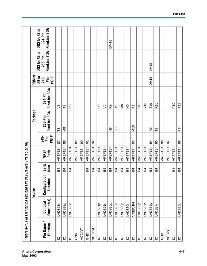
Pin List
IOLV
DS
93n
B4
VR
EF
1B4
87T
8V
8
IOLV
DS
92p
B4
VR
EF
1B4
88M
8T
8
IOLV
DS
92n
B4
VR
EF
1B4
R8
GN
DV
RE
F1B
489
VC
CIN
TV
RE
F1B
490
GN
DB
4V
RE
F1B
491
VC
CIO
4B
4V
RE
F1B
492
IOLV
DS
91p
B4
VR
EF
1B4
U9
IOLV
DS
91n
B4
VR
EF
1B4
V9
IOLV
DS
90p
B4
VR
EF
1B4
N8
R9
DM
1B
IOLV
DS
90n
B4
VR
EF
1B4
P8
T9
IOLV
DS
89p
B4
VR
EF
1B4
M9
IOLV
DS
89n
B4
VR
EF
1B4
N9
IOV
RE
F1B
4B
4V
RE
F1B
493
M10
P9
IOLV
DS
88p
B4
VR
EF
1B4
U10
IOLV
DS
88n
B4
VR
EF
1B4
V10
IOLV
DS
87p
B4
VR
EF
1B4
94R
9T
10D
M1B
DM
1B
IOLV
DS
87n
B4
VR
EF
1B4
95T
9R
10
GN
DV
RE
F1B
496
VC
CIN
TV
RE
F1B
497
IOB
4V
RE
F1B
4P
10
IOLV
DS
86p
B4
VR
EF
1B4
98P
9R
11
Tabl
e4–
1.Pi
n Li
st fo
r the
Cyc
lone
EP1
C12
Devi
ce (
Part
6of
18)
Dev
ice
Pack
age
DQS
for
X8 in
24
0-Pi
n PQ
FP
DQS
for X
8 in
25
6-Pi
n Fi
neLi
neBG
A
DQS
for X
8 in
32
4-Pi
n Fi
neLi
neBG
APi
n N
ame
/ Fu
nctio
nOp
tiona
l Fu
nctio
n(s)
Conf
igur
atio
n Fu
nctio
nBa
nk
Num
.VR
EF
Bank
240-
Pin
PQFP
256-
Pin
Fine
Line
BGA
324-
Pin
Fine
Line
BGA
Altera Corporation 4–7May 2003 Preliminary
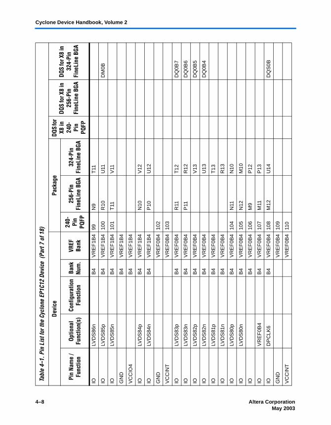
Cyclone Device Handbook, Volume 2
IOLV
DS
86n
B4
VR
EF
1B4
99N
9T
11
IOLV
DS
85p
B4
VR
EF
1B4
100
R10
U11
DM
0B
IOLV
DS
85n
B4
VR
EF
1B4
101
T11
V11
GN
DB
4V
RE
F1B
4
VC
CIO
4B
4V
RE
F1B
4
IOLV
DS
84p
B4
VR
EF
1B4
N10
V12
IOLV
DS
84n
B4
VR
EF
1B4
P10
U12
GN
DV
RE
F0B
410
2
VC
CIN
TV
RE
F0B
410
3
IOLV
DS
83p
B4
VR
EF
0B4
R11
T12
DQ
0B7
IOLV
DS
83n
B4
VR
EF
0B4
P11
R12
DQ
0B6
IOLV
DS
82p
B4
VR
EF
0B4
V13
DQ
0B5
IOLV
DS
82n
B4
VR
EF
0B4
U13
DQ
0B4
IOLV
DS
81p
B4
VR
EF
0B4
T13
IOLV
DS
81n
B4
VR
EF
0B4
R13
IOLV
DS
80p
B4
VR
EF
0B4
104
N11
N10
IOLV
DS
80n
B4
VR
EF
0B4
105
N12
M10
IOB
4V
RE
F0B
410
6M
9P
12
IOV
RE
F0B
4B
4V
RE
F0B
410
7M
11P
13
IOD
PC
LK6
B4
VR
EF
0B4
108
M12
U14
DQ
S0B
GN
DV
RE
F0B
410
9
VC
CIN
TV
RE
F0B
411
0
Tabl
e4–
1.Pi
n Li
st fo
r the
Cyc
lone
EP1
C12
Devi
ce (
Part
7of
18)
Dev
ice
Pack
age
DQS
for
X8 in
24
0-Pi
n PQ
FP
DQS
for X
8 in
25
6-Pi
n Fi
neLi
neBG
A
DQS
for X
8 in
32
4-Pi
n Fi
neLi
neBG
APi
n N
ame
/ Fu
nctio
nOp
tiona
l Fu
nctio
n(s)
Conf
igur
atio
n Fu
nctio
nBa
nk
Num
.VR
EF
Bank
240-
Pin
PQFP
256-
Pin
Fine
Line
BGA
324-
Pin
Fine
Line
BGA
4–8 Altera CorporationPreliminary May 2003

Pin List
GN
DB
4V
RE
F0B
411
1
VC
CIO
4B
4V
RE
F0B
411
2
IOLV
DS
79p
B4
VR
EF
0B4
113
P12
T14
DQ
1B3
DQ
1B3
DQ
0B3
IOLV
DS
79n
B4
VR
EF
0B4
114
R12
R14
DQ
1B2
DQ
1B2
DQ
0B2
IOLV
DS
78p
B4
VR
EF
0B4
115
T13
V15
DQ
1B1
DQ
1B1
DQ
0B1
IOLV
DS
78n
B4
VR
EF
0B4
116
R13
U15
DQ
1B0
DQ
1B0
DQ
0B0
IOLV
DS
77p
B4
VR
EF
0B4
117
R14
N11
IOLV
DS
77n
B4
VR
EF
0B4
118
P13
M11
IOLV
DS
76p
B4
VR
EF
0B4
119
T15
U16
IOLV
DS
76n
B4
VR
EF
0B4
120
R15
T15
IOLV
DS
75n
B3
VR
EF
2B3
121
N13
T16
IOLV
DS
75p
B3
VR
EF
2B3
122
P14
T17
IOLV
DS
74n
B3
VR
EF
2B3
123
P15
R17
IOLV
DS
74p
B3
VR
EF
2B3
124
R16
R18
IOLV
DS
73n
B3
VR
EF
2B3
125
N15
R15
DQ
1R7
DQ
1R7
DQ
1R7
IOLV
DS
73p
B3
VR
EF
2B3
126
N16
R16
IOV
RE
F2B
3B
3V
RE
F2B
312
7K
12P
16
IOB
3V
RE
F2B
312
8K
14P
17D
Q1R
6D
Q1R
6D
Q1R
6
GN
DB
3V
RE
F2B
312
9
VC
CIO
3B
3V
RE
F2B
313
0
IOD
PC
LK5
B3
VR
EF
2B3
131
L12
P15
DQ
S1R
DQ
S1R
DQ
S1R
IOLV
DS
72n
B3
VR
EF
2B3
132
N14
P14
DQ
1R5
DQ
1R5
DQ
1R5
Tabl
e4–
1.Pi
n Li
st fo
r the
Cyc
lone
EP1
C12
Devi
ce (
Part
8of
18)
Dev
ice
Pack
age
DQS
for
X8 in
24
0-Pi
n PQ
FP
DQS
for X
8 in
25
6-Pi
n Fi
neLi
neBG
A
DQS
for X
8 in
32
4-Pi
n Fi
neLi
neBG
APi
n N
ame
/ Fu
nctio
nOp
tiona
l Fu
nctio
n(s)
Conf
igur
atio
n Fu
nctio
nBa
nk
Num
.VR
EF
Bank
240-
Pin
PQFP
256-
Pin
Fine
Line
BGA
324-
Pin
Fine
Line
BGA
Altera Corporation 4–9May 2003 Preliminary

Cyclone Device Handbook, Volume 2
IOLV
DS
72p
B3
VR
EF
2B3
133
M13
N14
DQ
1R4
DQ
1R4
DQ
1R4
IOLV
DS
71n
B3
VR
EF
2B3
134
M14
N18
IOLV
DS
71p
B3
VR
EF
2B3
135
L13
N17
IOLV
DS
70n
B3
VR
EF
2B3
136
M15
N13
IOLV
DS
70p
B3
VR
EF
2B3
137
M16
N12
IOLV
DS
69n
B3
VR
EF
2B3
138
L14
N16
IOLV
DS
69p
B3
VR
EF
2B3
139
L15
N15
IOLV
DS
68n
B3
VR
EF
2B3
140
L16
M18
IOLV
DS
68p
B3
VR
EF
2B3
141
K16
M17
DQ
1R3
IOLV
DS
67n
B3
VR
EF
2B3
M14
DQ
1R2
IOLV
DS
67p
B3
VR
EF
2B3
M15
DQ
1R1
IOB
3V
RE
F2B
3M
16D
Q1R
0
GN
DB
3V
RE
F2B
314
2
VC
CIO
3B
3V
RE
F2B
3
IOLV
DS
66n
B3
VR
EF
1B3
L18
IOLV
DS
66p
B3
VR
EF
1B3
L17
IOLV
DS
65n
B3
VR
EF
1B3
M13
IOLV
DS
65p
B3
VR
EF
1B3
L13
IOLV
DS
64n
B3
VR
EF
1B3
L16
DM
1R
IOLV
DS
64p
B3
VR
EF
1B3
L15
IOB
3V
RE
F1B
3L1
4
IOP
LL2_
OU
Tn
B3
VR
EF
1B3
143
K15
K16
Tabl
e4–
1.Pi
n Li
st fo
r the
Cyc
lone
EP1
C12
Devi
ce (
Part
9of
18)
Dev
ice
Pack
age
DQS
for
X8 in
24
0-Pi
n PQ
FP
DQS
for X
8 in
25
6-Pi
n Fi
neLi
neBG
A
DQS
for X
8 in
32
4-Pi
n Fi
neLi
neBG
APi
n N
ame
/ Fu
nctio
nOp
tiona
l Fu
nctio
n(s)
Conf
igur
atio
n Fu
nctio
nBa
nk
Num
.VR
EF
Bank
240-
Pin
PQFP
256-
Pin
Fine
Line
BGA
324-
Pin
Fine
Line
BGA
4–10 Altera CorporationPreliminary May 2003

Pin List
IOP
LL2_
OU
Tp
B3
VR
EF
1B3
144
J16
K15
CO
NF
_DO
NE
CO
NF
_DO
NE
B3
VR
EF
1B3
145
K13
K17
nSTA
TU
SnS
TAT
US
B3
VR
EF
1B3
146
J13
L12
TC
KT
CK
B3
VR
EF
1B3
147
J14
K18
TM
ST
MS
B3
VR
EF
1B3
148
J15
K14
TD
OT
DO
B3
VR
EF
1B3
149
H15
K13
GN
DG
_PLL
2V
RE
F1B
315
0J1
2J1
8
GN
DA
_PLL
2V
RE
F1B
315
1J1
1K
12
CLK
3LV
DS
CLK
2nB
3V
RE
F1B
315
2H
16J1
6
CLK
2LV
DS
CLK
2pB
3V
RE
F1B
315
3G
16J1
5
VC
CA
_PLL
2V
RE
F1B
315
4H
11J1
2
TD
IT
DI
B3
VR
EF
1B3
155
H14
J17
IOV
RE
F1B
3B
3V
RE
F1B
315
6H
12J1
4
IOLV
DS
63n
B3
VR
EF
1B3
J13
IOLV
DS
63p
B3
VR
EF
1B3
H13
DM
0R
IOLV
DS
62n
B3
VR
EF
1B3
H14
IOLV
DS
62p
B3
VR
EF
1B3
H15
IOLV
DS
61n
B3
VR
EF
1B3
H16
IOLV
DS
61p
B3
VR
EF
1B3
H17
GN
DB
3V
RE
F0B
3
VC
CIO
3B
3V
RE
F0B
315
7
IOB
3V
RE
F0B
3H
18D
Q0R
7
Tabl
e4–
1.Pi
n Li
st fo
r the
Cyc
lone
EP1
C12
Devi
ce (
Part
10of
18)
Dev
ice
Pack
age
DQS
for
X8 in
24
0-Pi
n PQ
FP
DQS
for X
8 in
25
6-Pi
n Fi
neLi
neBG
A
DQS
for X
8 in
32
4-Pi
n Fi
neLi
neBG
APi
n N
ame
/ Fu
nctio
nOp
tiona
l Fu
nctio
n(s)
Conf
igur
atio
n Fu
nctio
nBa
nk
Num
.VR
EF
Bank
240-
Pin
PQFP
256-
Pin
Fine
Line
BGA
324-
Pin
Fine
Line
BGA
Altera Corporation 4–11May 2003 Preliminary
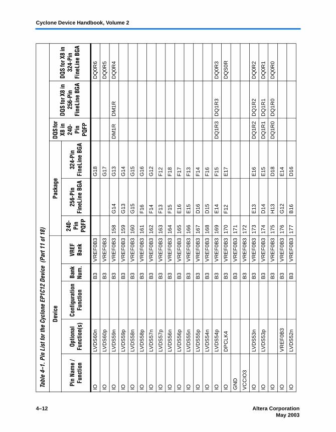
Cyclone Device Handbook, Volume 2
IOLV
DS
60n
B3
VR
EF
0B3
G18
DQ
0R6
IOLV
DS
60p
B3
VR
EF
0B3
G17
DQ
0R5
IOLV
DS
59n
B3
VR
EF
0B3
158
G14
G13
DM
1RD
M1R
DQ
0R4
IOLV
DS
59p
B3
VR
EF
0B3
159
G13
G14
IOLV
DS
58n
B3
VR
EF
0B3
160
G15
G15
IOLV
DS
58p
B3
VR
EF
0B3
161
F16
G16
IOLV
DS
57n
B3
VR
EF
0B3
162
F14
G12
IOLV
DS
57p
B3
VR
EF
0B3
163
F13
F12
IOLV
DS
56n
B3
VR
EF
0B3
164
F15
F18
IOLV
DS
56p
B3
VR
EF
0B3
165
E16
F17
IOLV
DS
55n
B3
VR
EF
0B3
166
E15
F13
IOLV
DS
55p
B3
VR
EF
0B3
167
D16
F14
IOLV
DS
54n
B3
VR
EF
0B3
168
D15
F16
IOLV
DS
54p
B3
VR
EF
0B3
169
E14
F15
DQ
1R3
DQ
1R3
DQ
0R3
IOD
PC
LK4
B3
VR
EF
0B3
170
F12
E17
DQ
S0R
GN
DB
3V
RE
F0B
317
1
VC
CIO
3B
3V
RE
F0B
317
2
IOLV
DS
53n
B3
VR
EF
0B3
173
E13
E16
DQ
1R2
DQ
1R2
DQ
0R2
IOLV
DS
53p
B3
VR
EF
0B3
174
D14
E15
DQ
1R1
DQ
1R1
DQ
0R1
IOB
3V
RE
F0B
317
5H
13D
18D
Q1R
0D
Q1R
0D
Q0R
0
IOV
RE
F0B
3B
3V
RE
F0B
317
6G
12E
14
IOLV
DS
52n
B3
VR
EF
0B3
177
B16
D16
Tabl
e4–
1.Pi
n Li
st fo
r the
Cyc
lone
EP1
C12
Devi
ce (
Part
11of
18)
Dev
ice
Pack
age
DQS
for
X8 in
24
0-Pi
n PQ
FP
DQS
for X
8 in
25
6-Pi
n Fi
neLi
neBG
A
DQS
for X
8 in
32
4-Pi
n Fi
neLi
neBG
APi
n N
ame
/ Fu
nctio
nOp
tiona
l Fu
nctio
n(s)
Conf
igur
atio
n Fu
nctio
nBa
nk
Num
.VR
EF
Bank
240-
Pin
PQFP
256-
Pin
Fine
Line
BGA
324-
Pin
Fine
Line
BGA
4–12 Altera CorporationPreliminary May 2003

Pin List
IOLV
DS
52p
B3
VR
EF
0B3
178
C15
D15
IOLV
DS
51n
B3
VR
EF
0B3
179
C14
C17
IOLV
DS
51p
B3
VR
EF
0B3
180
D13
D17
IOLV
DS
50n
B2
VR
EF
0B2
181
B15
C16
IOLV
DS
50p
B2
VR
EF
0B2
182
A15
B16
IOLV
DS
49n
B2
VR
EF
0B2
183
B14
G11
IOLV
DS
49p
B2
VR
EF
0B2
184
C13
F11
IOLV
DS
48n
B2
VR
EF
0B2
185
B13
B15
DQ
0T0
DQ
0T0
DQ
0T0
IOLV
DS
48p
B2
VR
EF
0B2
186
A13
A15
DQ
0T1
DQ
0T1
DQ
0T1
IOLV
DS
47n
B2
VR
EF
0B2
187
B12
C15
DQ
0T2
DQ
0T2
DQ
0T2
IOLV
DS
47p
B2
VR
EF
0B2
188
C12
D14
DQ
0T3
DQ
0T3
DQ
0T3
VC
CIO
2B
2V
RE
F0B
218
9
GN
DB
2V
RE
F0B
219
0
VC
CIN
TV
RE
F0B
219
1
GN
DV
RE
F0B
219
2
IOD
PC
LK3
B2
VR
EF
0B2
193
E12
B14
DQ
S0T
DQ
S0T
DQ
S0T
IOV
RE
F0B
2B
2V
RE
F0B
219
4E
11C
14
IOB
2V
RE
F0B
219
5E
9E
13
IOLV
DS
46n
B2
VR
EF
0B2
196
D12
G10
IOLV
DS
46p
B2
VR
EF
0B2
197
D11
F10
IOLV
DS
45n
B2
VR
EF
0B2
B13
IOLV
DS
45p
B2
VR
EF
0B2
A13
Tabl
e4–
1.Pi
n Li
st fo
r the
Cyc
lone
EP1
C12
Devi
ce (
Part
12of
18)
Dev
ice
Pack
age
DQS
for
X8 in
24
0-Pi
n PQ
FP
DQS
for X
8 in
25
6-Pi
n Fi
neLi
neBG
A
DQS
for X
8 in
32
4-Pi
n Fi
neLi
neBG
APi
n N
ame
/ Fu
nctio
nOp
tiona
l Fu
nctio
n(s)
Conf
igur
atio
n Fu
nctio
nBa
nk
Num
.VR
EF
Bank
240-
Pin
PQFP
256-
Pin
Fine
Line
BGA
324-
Pin
Fine
Line
BGA
Altera Corporation 4–13May 2003 Preliminary
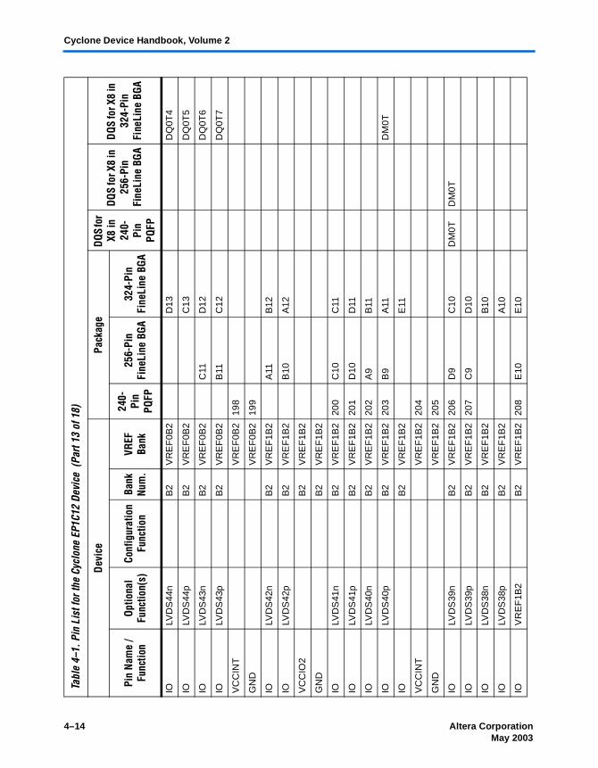
Cyclone Device Handbook, Volume 2
IOLV
DS
44n
B2
VR
EF
0B2
D13
DQ
0T4
IOLV
DS
44p
B2
VR
EF
0B2
C13
DQ
0T5
IOLV
DS
43n
B2
VR
EF
0B2
C11
D12
DQ
0T6
IOLV
DS
43p
B2
VR
EF
0B2
B11
C12
DQ
0T7
VC
CIN
TV
RE
F0B
219
8
GN
DV
RE
F0B
219
9
IOLV
DS
42n
B2
VR
EF
1B2
A11
B12
IOLV
DS
42p
B2
VR
EF
1B2
B10
A12
VC
CIO
2B
2V
RE
F1B
2
GN
DB
2V
RE
F1B
2
IOLV
DS
41n
B2
VR
EF
1B2
200
C10
C11
IOLV
DS
41p
B2
VR
EF
1B2
201
D10
D11
IOLV
DS
40n
B2
VR
EF
1B2
202
A9
B11
IOLV
DS
40p
B2
VR
EF
1B2
203
B9
A11
DM
0T
IOB
2V
RE
F1B
2E
11
VC
CIN
TV
RE
F1B
220
4
GN
DV
RE
F1B
220
5
IOLV
DS
39n
B2
VR
EF
1B2
206
D9
C10
DM
0TD
M0T
IOLV
DS
39p
B2
VR
EF
1B2
207
C9
D10
IOLV
DS
38n
B2
VR
EF
1B2
B10
IOLV
DS
38p
B2
VR
EF
1B2
A10
IOV
RE
F1B
2B
2V
RE
F1B
220
8E
10E
10
Tabl
e4–
1.Pi
n Li
st fo
r the
Cyc
lone
EP1
C12
Devi
ce (
Part
13of
18)
Dev
ice
Pack
age
DQS
for
X8 in
24
0-Pi
n PQ
FP
DQS
for X
8 in
25
6-Pi
n Fi
neLi
neBG
A
DQS
for X
8 in
32
4-Pi
n Fi
neLi
neBG
APi
n N
ame
/ Fu
nctio
nOp
tiona
l Fu
nctio
n(s)
Conf
igur
atio
n Fu
nctio
nBa
nk
Num
.VR
EF
Bank
240-
Pin
PQFP
256-
Pin
Fine
Line
BGA
324-
Pin
Fine
Line
BGA
4–14 Altera CorporationPreliminary May 2003
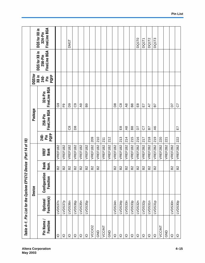
Pin List
IOLV
DS
37n
B2
VR
EF
1B2
G9
IOLV
DS
37p
B2
VR
EF
1B2
F9
IOLV
DS
36n
B2
VR
EF
1B2
C8
D9
DM
1T
IOLV
DS
36p
B2
VR
EF
1B2
D8
C9
IOLV
DS
35n
B2
VR
EF
1B2
A9
IOLV
DS
35p
B2
VR
EF
1B2
B9
VC
CIO
2B
2V
RE
F1B
220
9
GN
DB
2V
RE
F1B
221
0
VC
CIN
TV
RE
F1B
221
1
GN
DV
RE
F1B
221
2
IOLV
DS
34n
B2
VR
EF
1B2
D8
IOLV
DS
34p
B2
VR
EF
1B2
213
E8
C8
IOLV
DS
33n
B2
VR
EF
1B2
214
A8
A8
IOLV
DS
33p
B2
VR
EF
1B2
215
B8
B8
IOLV
DS
32n
B2
VR
EF
2B2
216
D7
E8
DQ
1T0
IOLV
DS
32p
B2
VR
EF
2B2
217
C7
E7
DQ
1T1
IOLV
DS
31n
B2
VR
EF
2B2
218
B7
A7
DQ
1T2
IOLV
DS
31p
B2
VR
EF
2B2
219
A6
B7
DQ
1T3
VC
CIN
TV
RE
F2B
222
0
GN
DV
RE
F2B
222
1
IOLV
DS
30n
B2
VR
EF
2B2
D7
IOLV
DS
30p
B2
VR
EF
2B2
222
E7
C7
Tabl
e4–
1.Pi
n Li
st fo
r the
Cyc
lone
EP1
C12
Devi
ce (
Part
14of
18)
Dev
ice
Pack
age
DQS
for
X8 in
24
0-Pi
n PQ
FP
DQS
for X
8 in
25
6-Pi
n Fi
neLi
neBG
A
DQS
for X
8 in
32
4-Pi
n Fi
neLi
neBG
APi
n N
ame
/ Fu
nctio
nOp
tiona
l Fu
nctio
n(s)
Conf
igur
atio
n Fu
nctio
nBa
nk
Num
.VR
EF
Bank
240-
Pin
PQFP
256-
Pin
Fine
Line
BGA
324-
Pin
Fine
Line
BGA
Altera Corporation 4–15May 2003 Preliminary

Cyclone Device Handbook, Volume 2
IOLV
DS
29n
B2
VR
EF
2B2
223
B6
E6
IOLV
DS
29p
B2
VR
EF
2B2
224
C6
D6
IOLV
DS
28n
B2
VR
EF
2B2
225
D6
B6
IOLV
DS
28p
B2
VR
EF
2B2
226
D5
C6
IOV
RE
F2B
2B
2V
RE
F2B
222
7E
6A
6
IOD
PC
LK2
B2
VR
EF
2B2
228
E5
B5
DQ
S1T
VC
CIN
TV
RE
F2B
222
9
GN
DV
RE
F2B
223
0
VC
CIO
2B
2V
RE
F2B
223
1
GN
DB
2V
RE
F2B
223
2
IOLV
DS
27n
B2
VR
EF
2B2
233
C5
C5
DQ
0T4
DQ
0T4
DQ
1T4
IOLV
DS
27p
B2
VR
EF
2B2
234
B5
D5
DQ
0T5
DQ
0T5
DQ
1T5
IOLV
DS
26n
B2
VR
EF
2B2
235
A4
A4
DQ
0T6
DQ
0T6
DQ
1T6
IOLV
DS
26p
B2
VR
EF
2B2
236
B4
B4
DQ
0T7
DQ
0T7
DQ
1T7
IOLV
DS
25n
B2
VR
EF
2B2
237
C4
F8
IOLV
DS
25p
B2
VR
EF
2B2
238
B3
G8
IOLV
DS
24n
DE
V_O
EB
2V
RE
F2B
223
9A
2B
3
IOLV
DS
24p
DE
V_C
LRn
B2
VR
EF
2B2
240
B2
C4
VC
CIN
TA
7A
17
VC
CIN
TA
10A
2
VC
CIN
TG
8B
1
VC
CIN
TG
10B
18
Tabl
e4–
1.Pi
n Li
st fo
r the
Cyc
lone
EP1
C12
Devi
ce (
Part
15of
18)
Dev
ice
Pack
age
DQS
for
X8 in
24
0-Pi
n PQ
FP
DQS
for X
8 in
25
6-Pi
n Fi
neLi
neBG
A
DQS
for X
8 in
32
4-Pi
n Fi
neLi
neBG
APi
n N
ame
/ Fu
nctio
nOp
tiona
l Fu
nctio
n(s)
Conf
igur
atio
n Fu
nctio
nBa
nk
Num
.VR
EF
Bank
240-
Pin
PQFP
256-
Pin
Fine
Line
BGA
324-
Pin
Fine
Line
BGA
4–16 Altera CorporationPreliminary May 2003

Pin List
VC
CIN
TH
7H
10
VC
CIN
TH
9J9
VC
CIN
TJ8
K10
VC
CIN
TJ1
0L9
VC
CIN
TK
7U
1
VC
CIN
TK
9U
18
VC
CIN
TT
7V
17
VC
CIN
TT
10V
2
VC
CIO
1C
1
VC
CIO
1G
6E
1
VC
CIO
1P
1G
7
VC
CIO
1M
7
VC
CIO
1P
1
VC
CIO
4T
3
VC
CIO
4L7
P11
VC
CIO
4L1
0P
8
VC
CIO
4T
14V
14
VC
CIO
4V
5
VC
CIO
3P
16
VC
CIO
3K
11E
18
VC
CIO
3C
16H
12
VC
CIO
3M
12
Tabl
e4–
1.Pi
n Li
st fo
r the
Cyc
lone
EP1
C12
Devi
ce (
Part
16of
18)
Dev
ice
Pack
age
DQS
for
X8 in
24
0-Pi
n PQ
FP
DQS
for X
8 in
25
6-Pi
n Fi
neLi
neBG
A
DQS
for X
8 in
32
4-Pi
n Fi
neLi
neBG
APi
n N
ame
/ Fu
nctio
nOp
tiona
l Fu
nctio
n(s)
Conf
igur
atio
n Fu
nctio
nBa
nk
Num
.VR
EF
Bank
240-
Pin
PQFP
256-
Pin
Fine
Line
BGA
324-
Pin
Fine
Line
BGA
Altera Corporation 4–17May 2003 Preliminary

Cyclone Device Handbook, Volume 2
VC
CIO
3P
18
VC
CIO
2A
14
VC
CIO
2F
10A
14
VC
CIO
2F
7A
5
VC
CIO
2A
3E
12
VC
CIO
2E
9
GN
DA
1A
1
GN
DA
16A
16
GN
DA
5A
18
GN
DA
12A
3
GN
DF
6B
17
GN
DF
8B
2
GN
DF
9C
1
GN
DF
11C
18
GN
DG
7H
11
GN
DG
9H
8
GN
DG
11H
9
GN
DH
8J1
0
GN
DH
10J1
1
GN
DJ7
J8
GN
DJ9
K11
GN
DK
6K
8
Tabl
e4–
1.Pi
n Li
st fo
r the
Cyc
lone
EP1
C12
Devi
ce (
Part
17of
18)
Dev
ice
Pack
age
DQS
for
X8 in
24
0-Pi
n PQ
FP
DQS
for X
8 in
25
6-Pi
n Fi
neLi
neBG
A
DQS
for X
8 in
32
4-Pi
n Fi
neLi
neBG
APi
n N
ame
/ Fu
nctio
nOp
tiona
l Fu
nctio
n(s)
Conf
igur
atio
n Fu
nctio
nBa
nk
Num
.VR
EF
Bank
240-
Pin
PQFP
256-
Pin
Fine
Line
BGA
324-
Pin
Fine
Line
BGA
4–18 Altera CorporationPreliminary May 2003

Pin List
GN
DK
8K
9
GN
DK
10L1
0
GN
DL6
L11
GN
DL8
L8
GN
DL9
T1
GN
DL1
1T
18
GN
DT
1U
17
GN
DT
5U
2
GN
DT
12V
1
GN
DT
16V
16
GN
DV
18
GN
DV
3
Tabl
e4–
1.Pi
n Li
st fo
r the
Cyc
lone
EP1
C12
Devi
ce (
Part
18of
18)
Dev
ice
Pack
age
DQS
for
X8 in
24
0-Pi
n PQ
FP
DQS
for X
8 in
25
6-Pi
n Fi
neLi
neBG
A
DQS
for X
8 in
32
4-Pi
n Fi
neLi
neBG
APi
n N
ame
/ Fu
nctio
nOp
tiona
l Fu
nctio
n(s)
Conf
igur
atio
n Fu
nctio
nBa
nk
Num
.VR
EF
Bank
240-
Pin
PQFP
256-
Pin
Fine
Line
BGA
324-
Pin
Fine
Line
BGA
Altera Corporation 4–19May 2003 Preliminary

Cyclone Device Handbook, Volume 2
Pin
Defin
ition
sTa
ble
4–2
show
s p
in d
efin
itio
ns fo
r th
e E
P1C
12 d
evic
e.
Tabl
e4–
2.Pi
n De
finiti
ons
for t
he E
P1C1
2 De
vice
(Pa
rt1
of4)
Pin
Nam
ePi
n Ty
pe (1
st, 2
nd, &
3r
d Fu
nctio
n)Pi
n De
scrip
tion
Supp
ly a
nd R
efer
ence
Pin
s
VC
CIO
[1..4
]P
ower
The
se a
re I/
O s
uppl
y vo
ltage
pin
s fo
r ba
nks
1 th
roug
h 4.
Eac
h ba
nk c
an s
uppo
rt a
diff
eren
t vol
tage
le
vel.
VC
CIO
sup
plie
s po
wer
to th
e ou
tput
buf
fers
for a
ll I/O
sta
ndar
ds. V
CC
IO a
lso
supp
lies
pow
er to
th
e in
put b
uffe
rs u
sed
for
the
LVT
TL,
LV
CM
OS
, 1.5
-V, 1
.8-V
, 2.5
-V, a
nd 3
.3-V
PC
I I/O
sta
ndar
ds.
VC
CIN
TP
ower
The
se a
re in
tern
al lo
gic
arra
y vo
ltage
sup
ply
pins
. VC
CIN
T a
lso
supp
lies
pow
er to
the
inpu
t buf
fers
us
ed fo
r th
e LV
DS
, SS
TL2
, and
SS
TL3
I/O
sta
ndar
ds.
VR
EF
[0..2
]B[1
..4]
I/O, I
nput
zIn
put r
efer
ence
vol
tage
for
bank
s 1-
4. If
a b
ank
uses
a v
olta
ge-r
efer
ence
d I/O
sta
ndar
d, th
en th
ese
pins
are
use
d as
the
volta
ge-r
efer
ence
pin
s fo
r th
e ba
nk. I
f vol
tage
ref
eren
ce I/
O s
tand
ards
are
not
us
ed in
the
bank
, the
VR
EF
pin
s ar
e av
aila
ble
as u
ser
I/O p
ins.
VC
CA
_PLL
[1..2
]P
ower
Ana
log
pow
er fo
r P
LLs[
1..2
]. T
he d
esig
ner
mus
t con
nect
this
pin
to 1
.5 V
, eve
n if
the
PLL
is n
ot u
sed.
GN
DA
_PLL
[1..2
]G
roun
dA
nalo
g gr
ound
for
PLL
s[1.
.2].
The
des
igne
r ca
n co
nnec
t thi
s pi
n to
the
GN
D p
lane
on
the
boar
d.
GN
DG
_PLL
[1..2
]G
roun
dG
uard
rin
g gr
ound
for
PLL
s[1.
.2].
The
des
igne
r ca
n co
nnec
t thi
s pi
n to
the
GN
D p
lane
on
the
boar
d.
Conf
igur
atio
n an
d JT
AG P
ins
CO
NF
_DO
NE
Bid
irect
iona
l (op
en-
drai
n)T
his
is a
ded
icat
ed c
onfig
urat
ion
stat
us p
in; i
t is
not a
vaila
ble
as a
use
r I/O
pin
.
nSTA
TU
SB
idire
ctio
nal (
open
-dr
ain)
Thi
s is
a d
edic
ated
con
figur
atio
n st
atus
pin
; it i
s no
t ava
ilabl
e as
a u
ser
I/O p
in.
nCO
NF
IGIn
put
Ded
icat
ed c
onfig
urat
ion
cont
rol i
nput
. A lo
w tr
ansi
tion
rese
ts th
e ta
rget
dev
ice;
a lo
w-t
o-hi
gh tr
ansi
tion
begi
ns c
onfig
urat
ion.
All
I/O p
ins
tri-s
tate
whe
n nC
ON
FIG
is d
riven
low
.
DC
LKIn
put (
PS
mod
e),
Out
put (
AS
mod
e)In
pas
sive
ser
ial c
onfig
urat
ion
mod
e, D
CLK
is a
clo
ck in
put u
sed
to c
lock
con
figur
atio
n da
ta fr
om a
n ex
tern
al s
ourc
e in
to th
e C
yclo
ne d
evic
e. In
act
ive
seria
l con
figur
atio
n m
ode,
DC
LK is
a c
lock
out
put
from
the
Cyc
lone
dev
ice
(the
Cyc
lone
dev
ice
acts
as
mas
ter i
n th
is m
ode)
. Thi
s is
a d
edic
ated
pin
use
d fo
r co
nfig
urat
ion.
DA
TA0
Inpu
tD
edic
ated
con
figur
atio
n da
ta in
put p
in.
4–20 Altera CorporationPreliminary May 2003

Pin Definitions
nCE
Inpu
tA
ctiv
e-lo
w c
hip
enab
le. D
edic
ated
chi
p en
able
inpu
t use
d to
det
ect w
hich
dev
ice
is a
ctiv
e in
a c
hain
of
devi
ces.
Whe
n nC
E is
low
, the
dev
ice
is e
nabl
ed. W
hen
nCE
is h
igh,
the
devi
ce is
dis
able
d.
nCE
OO
utpu
tO
utpu
t tha
t driv
es lo
w w
hen
devi
ce c
onfig
urat
ion
is c
ompl
ete.
Dur
ing
mul
ti-de
vice
con
figur
atio
n, th
is
pin
feed
s a
subs
eque
nt d
evic
e’s
nCE
pin
.
AS
DO
I/O, O
utpu
tA
ctiv
e se
rial d
ata
outp
ut fr
om th
e C
yclo
ne d
evic
e. T
his
outp
ut p
in is
util
ized
dur
ing
activ
e se
rial
conf
igur
atio
n m
ode.
The
Cyc
lone
dev
ice
cont
rols
con
figur
atio
n an
d dr
ives
add
ress
and
con
trol
in
form
atio
n ou
t on
AS
DO
. In
pass
ive
seria
l con
figur
atio
n, th
is p
in is
ava
ilabl
e as
a u
ser
I/O p
in.
nCS
OI/O
, Out
put
Chi
p se
lect
out
put t
hat e
nabl
es/d
isab
les
a se
rial c
onfig
urat
ion
devi
ce.
Thi
s ou
tput
is u
tiliz
ed d
urin
g ac
tive
seria
l con
figur
atio
n m
ode.
The
Cyc
lone
dev
ice
cont
rols
con
figur
atio
n an
d en
able
s th
e se
rial
conf
igur
atio
n de
vice
by
driv
ing
nCS
O lo
w. I
n pa
ssiv
e se
rial c
onfig
urat
ion,
this
pin
is a
vaila
ble
as a
use
r I/O
pin
.
INIT
_DO
NE
I/O, O
utpu
t (op
en-
drai
n)T
his
is a
dua
l-pur
pose
pin
and
can
be
used
as
an I/
O p
in w
hen
not e
nabl
ed a
s IN
IT_D
ON
E. W
hen
enab
led,
the
pin
indi
cate
s w
hen
the
devi
ce h
as e
nter
ed u
ser m
ode.
Thi
s pi
n ca
n be
use
d as
a u
ser I
/O
pin
afte
r co
nfig
urat
ion.
CLK
US
RI/O
, Inp
utO
ptio
nal u
ser-
supp
lied
cloc
k in
put.
Syn
chro
nize
s th
e in
itial
izat
ion
of o
ne o
r mor
e de
vice
s. T
his
pin
can
be u
sed
as a
use
r I/O
pin
afte
r co
nfig
urat
ion.
DE
V_C
LRn
I/O, I
nput
Dua
l-pur
pose
pin
that
can
ove
rrid
e al
l cle
ars
on a
ll de
vice
reg
iste
rs. W
hen
this
pin
is d
riven
low
, all
regi
ster
s ar
e cl
eare
d; w
hen
this
pin
is d
riven
hig
h, a
ll re
gist
ers
beha
ve a
s de
fined
in th
e de
sign
.
DE
V_O
EI/O
, Inp
utD
ual-p
urpo
se p
in th
at c
an o
verr
ide
all t
ri-st
ates
on
the
devi
ce. W
hen
this
pin
is d
riven
low
, all
I/O p
ins
are
tri-s
tate
d; w
hen
this
pin
is d
riven
hig
h, a
ll I/O
pin
s be
have
as
defin
ed in
the
desi
gn.
MS
EL[
1..0
]In
put
Ded
icat
ed m
ode
sele
ct c
ontr
ol p
ins
that
set
the
conf
igur
atio
n m
ode
for
the
devi
ce.
TM
SIn
put
Thi
s is
a d
edic
ated
JTA
G in
put p
in.
TD
IIn
put
Thi
s is
a d
edic
ated
JTA
G in
put p
in.
TC
KIn
put
Thi
s is
a d
edic
ated
JTA
G in
put p
in.
TD
OO
utpu
tT
his
is a
ded
icat
ed J
TAG
out
put p
in.
Cloc
k an
d PL
L Pi
ns
CLK
0In
put,
LVD
S In
put
Ded
icat
ed g
loba
l clo
ck in
put.
The
dua
l-fun
ctio
n of
CLK
0 is
LV
DS
CLK
1p, w
hich
is u
sed
for
diffe
rent
ial
inpu
t to
PLL
1.
Tabl
e4–
2.Pi
n De
finiti
ons
for t
he E
P1C1
2 De
vice
(Pa
rt2
of4)
Pin
Nam
ePi
n Ty
pe (1
st, 2
nd, &
3r
d Fu
nctio
n)Pi
n De
scrip
tion
Altera Corporation 4–21May 2003 Preliminary

Cyclone Device Handbook, Volume 2
CLK
1In
put,
LVD
S In
put
Ded
icat
ed g
loba
l clo
ck in
put.
The
dua
l-fun
ctio
n of
CLK
1 is
LV
DS
CLK
1n, w
hich
is u
sed
for
diffe
rent
ial
inpu
t to
PLL
1.
CLK
2In
put,
LVD
S In
put
Ded
icat
ed g
loba
l clo
ck in
put.
The
dua
l-fun
ctio
n of
CLK
2 is
LV
DS
CLK
2p, w
hich
is u
sed
for
diffe
rent
ial
inpu
t to
PLL
2.
CLK
3In
put,
LVD
S In
put
Ded
icat
ed g
loba
l clo
ck in
put.
The
dua
l-fun
ctio
n of
CLK
3 is
LV
DS
CLK
2n, w
hich
is u
sed
for
diffe
rent
ial
inpu
t to
PLL
2.
DP
CLK
[7..0
]I/O
Dua
l-pur
pose
clo
ck p
ins
that
can
con
nect
to th
e gl
obal
clo
ck n
etw
ork.
The
se p
ins
can
be u
sed
for h
igh
fan-
out c
ontr
ol s
igna
ls, s
uch
as c
lock
s, c
lear
s, IR
DY,
TR
DY,
or
DQ
S s
igna
ls.
The
se p
ins
are
also
av
aila
ble
as u
ser
I/O p
ins.
PLL
1_O
UT
pI/O
, Out
put
Ext
erna
l clo
ck o
utpu
t fro
m P
LL 1
. Thi
s pi
n ca
n be
use
d w
ith d
iffer
entia
l or s
ingl
e en
ded
I/O s
tand
ards
. If
cloc
k ou
tput
from
PLL
1 is
not
use
d, th
is p
in is
ava
ilabl
e as
a u
ser
I/O p
in.
PLL
1_O
UT
nI/O
, Out
put
Neg
ativ
e te
rmin
al fo
r ex
tern
al c
lock
out
put f
rom
PLL
1. If
the
cloc
k ou
tput
is s
ingl
e en
ded,
this
pin
is
avai
labl
e as
a u
ser
I/O p
in.
PLL
2_O
UT
pI/O
, Out
put
Ext
erna
l clo
ck o
utpu
t fro
m P
LL 2
. Thi
s pi
n ca
n be
use
d w
ith d
iffer
entia
l or s
ingl
e en
ded
I/O s
tand
ards
. If
cloc
k ou
tput
from
PLL
2 is
not
use
d, th
is p
in is
ava
ilabl
e as
a u
ser
I/O p
in.
PLL
2_O
UT
nI/O
, Out
put
Neg
ativ
e te
rmin
al fo
r ex
tern
al c
lock
out
put f
rom
PLL
2. If
the
cloc
k ou
tput
is s
ingl
e en
ded,
this
pin
is
avai
labl
e as
a u
ser
I/O p
in.
Dua
l-Pur
pose
LVD
S &
Ext
erna
l Mem
ory
Inte
rface
Pin
s
LVD
S[0
..102
]pI/O
, LV
DS
RX
or
TX
Dua
l-pur
pose
LV
DS
I/O
cha
nnel
s 0
to 1
02. T
hese
cha
nnel
s ca
n be
use
d fo
r re
ceiv
ing
or tr
ansm
ittin
g LV
DS
com
patib
le s
igna
ls. P
ins
with
a "
p" s
uffix
car
ry th
e po
sitiv
e si
gnal
for
the
diffe
rent
ial c
hann
el. I
f no
t use
d fo
r LV
DS
inte
rfac
ing,
thes
e pi
ns a
re a
vaila
ble
as u
ser
I/O p
ins.
LVD
S[0
..102
]nI/O
, LV
DS
RX
or
TX
Dua
l-pur
pose
LV
DS
I/O
cha
nnel
s 0
to 1
02. T
hese
cha
nnel
s ca
n be
use
d fo
r re
ceiv
ing
or tr
ansm
ittin
g LV
DS
com
patib
le s
igna
ls. P
ins
with
an
"n"
suffi
x ca
rry
the
nega
tive
sign
al fo
r th
e di
ffere
ntia
l cha
nnel
. If
not u
sed
for
LVD
S in
terf
acin
g, th
ese
pins
are
ava
ilabl
e as
use
r I/O
pin
s.
LVD
SC
LK1p
Inpu
t, LV
DS
Inpu
tD
ual-p
urpo
se L
VD
S c
lock
inpu
t to
PLL
1. I
f diff
eren
tial i
nput
to P
LL1
is n
ot re
quire
d, th
is p
in is
ava
ilabl
e as
the
CLK
0 in
put p
in.
LVD
SC
LK1n
Inpu
t, LV
DS
Inpu
tD
ual-p
urpo
se L
VD
S c
lock
inpu
t to
PLL
1. I
f diff
eren
tial i
nput
to P
LL1
is n
ot re
quire
d, th
is p
in is
ava
ilabl
e as
the
CLK
1 in
put p
in.
Tabl
e4–
2.Pi
n De
finiti
ons
for t
he E
P1C1
2 De
vice
(Pa
rt3
of4)
Pin
Nam
ePi
n Ty
pe (1
st, 2
nd, &
3r
d Fu
nctio
n)Pi
n De
scrip
tion
4–22 Altera CorporationPreliminary May 2003
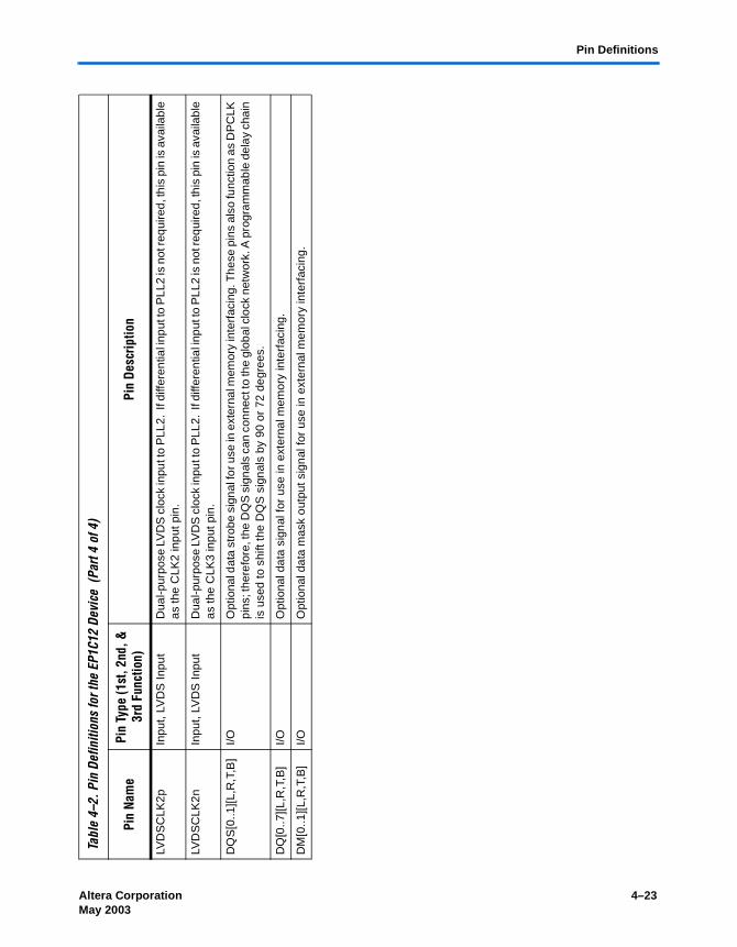
Pin Definitions
LVD
SC
LK2p
Inpu
t, LV
DS
Inpu
tD
ual-p
urpo
se L
VD
S c
lock
inpu
t to
PLL
2. I
f diff
eren
tial i
nput
to P
LL2
is n
ot re
quire
d, th
is p
in is
ava
ilabl
e as
the
CLK
2 in
put p
in.
LVD
SC
LK2n
Inpu
t, LV
DS
Inpu
tD
ual-p
urpo
se L
VD
S c
lock
inpu
t to
PLL
2. I
f diff
eren
tial i
nput
to P
LL2
is n
ot re
quire
d, th
is p
in is
ava
ilabl
e as
the
CLK
3 in
put p
in.
DQ
S[0
..1][L
,R,T
,B]
I/OO
ptio
nal d
ata
stro
be s
igna
l for
use
in e
xter
nal m
emor
y in
terf
acin
g. T
hese
pin
s al
so fu
nctio
n as
DP
CLK
pi
ns; t
here
fore
, the
DQ
S s
igna
ls c
an c
onne
ct to
the
glob
al c
lock
net
wor
k. A
pro
gram
mab
le d
elay
cha
in
is u
sed
to s
hift
the
DQ
S s
igna
ls b
y 90
or
72 d
egre
es.
DQ
[0..7
][L,R
,T,B
]I/O
Opt
iona
l dat
a si
gnal
for
use
in e
xter
nal m
emor
y in
terf
acin
g.
DM
[0..1
][L,R
,T,B
]I/O
Opt
iona
l dat
a m
ask
outp
ut s
igna
l for
use
in e
xter
nal m
emor
y in
terf
acin
g.
Tabl
e4–
2.Pi
n De
finiti
ons
for t
he E
P1C1
2 De
vice
(Pa
rt4
of4)
Pin
Nam
ePi
n Ty
pe (1
st, 2
nd, &
3r
d Fu
nctio
n)Pi
n De
scrip
tion
Altera Corporation 4–23May 2003 Preliminary
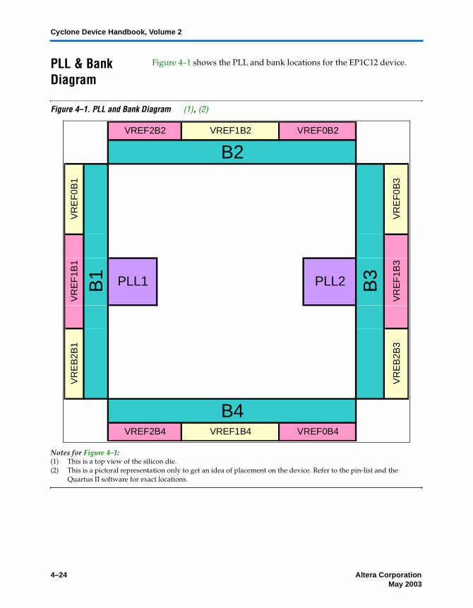
Cyclone Device Handbook, Volume 2
PLL & Bank Diagram
Figure 4–1 shows the PLL and bank locations for the EP1C12 device.
Figure 4–1. PLL and Bank Diagram (1), (2)
Notes for Figure 4–1:(1) This is a top view of the silicon die.(2) This is a pictoral representation only to get an idea of placement on the device. Refer to the pin-list and the
Quartus II software for exact locations.
VR
EB
2B3
B4VREF2B4 VREF1B4 VREF0B4
B3
VR
EF
0B3
VR
EF
1B3
VREF2B2 VREF1B2 VREF0B2
B2
VR
EF
0B1
B1
VR
EF
1B1
PLL1 PLL2
VR
EB
2B1
4–24 Altera CorporationPreliminary May 2003
Altera Corporation May 2003
C52005-1.0
5. Cyclone EP1C20 DevicePin Information
Introduction The following tables contain pin information for the Cyclone EP1C20 device, organized into the following sections:
Section Page
Pin List. . . . . . . . . . . . . . . . . . . . . . . . . . . . . . . . . . . . . . . . . . . . . . 5–2Pin Definitions . . . . . . . . . . . . . . . . . . . . . . . . . . . . . . . . . . . . . . 5–22PLL & Bank Diagram . . . . . . . . . . . . . . . . . . . . . . . . . . . . . . . . 5–26
5–1Preliminary

Cyclone Device Handbook, Volume 2
Pin
List
Tabl
e5–
1 sh
ows
the
com
ple
te p
in li
st fo
r th
e d
evic
e C
yclo
ne E
P1C
20 d
evic
e:
Tabl
e5–
1.Pi
n Li
st fo
r the
Cyc
lone
EP1
C20
Devi
ce (
Part
1of
20)
Devi
cePa
ckag
eDQ
S fo
r X8
in
324-
Pin
Fine
Line
BGA
DQS
for X
8 in
40
0-Pi
n Fi
neLi
neBG
APi
n Na
me
/ Fu
nctio
nO
ptio
nal
Func
tion(
s)Co
nfig
urat
ion
Func
tion
Bank
Nu
mbe
rVR
EF B
ank
324-
Pin
Fine
Line
BGA
400-
Pin
Fine
Line
BGA
IOLV
DS
31p
INIT
_DO
NE
B1
VR
EF
0B1
C3
C3
IOLV
DS
31n
B1
VR
EF
0B1
C2
C2
IOLV
DS
30p
CLK
US
RB
1V
RE
F0B
1D
3D
3
IOLV
DS
30n
B1
VR
EF
0B1
D2
D2
IOV
RE
F0B
1B
1V
RE
F0B
1D
4D
4
IOB
1V
RE
F0B
1D
1D
1
IOLV
DS
29p
B1
VR
EF
0B1
E3
E4
DQ
0L0
DQ
0L0
IOLV
DS
29n
B1
VR
EF
0B1
E2
E5
DQ
0L1
DQ
0L1
VC
CIO
1B
1V
RE
F0B
1
GN
DB
1V
RE
F0B
1
IOD
PC
LK1
B1
VR
EF
0B1
F1
F3
DQ
S0L
DQ
S0L
IOLV
DS
28p
B1
VR
EF
0B1
E4
E3
DQ
0L2
DQ
0L2
IOLV
DS
28n
B1
VR
EF
0B1
E5
E2
DQ
0L3
DQ
0L3
IOLV
DS
27p
B1
VR
EF
0B1
F2
F4
IOLV
DS
27n
B1
VR
EF
0B1
F3
F5
IOLV
DS
26p
B1
VR
EF
0B1
F4
F2
IOLV
DS
26n
B1
VR
EF
0B1
F5
F1
IOLV
DS
25p
B1
VR
EF
0B1
G1
F6
IOLV
DS
25n
B1
VR
EF
0B1
G2
G5
IOLV
DS
24p
B1
VR
EF
0B1
F6
G1
IOLV
DS
24n
B1
VR
EF
0B1
F7
G2
5–2 Altera CorporationPreliminary May 2003

Pin List
IOLV
DS
23p
B1
VR
EF
0B1
G3
G6
IOLV
DS
23n
B1
VR
EF
0B1
G4
G7
DQ
0L4
DQ
0L4
IOLV
DS
22p
B1
VR
EF
0B1
G5
G3
DQ
0L5
DQ
0L5
IOLV
DS
22n
B1
VR
EF
0B1
G6
G4
DQ
0L6
DQ
0L6
IOB
1V
RE
F0B
1H
1H
7D
Q0L
7D
Q0L
7
VC
CIO
1B
1V
RE
F0B
1
GN
DB
1V
RE
F0B
1
IOLV
DS
21p
B1
VR
EF
1B1
H2
H1
IOLV
DS
21n
B1
VR
EF
1B1
H3
H2
IOLV
DS
20p
B1
VR
EF
1B1
H4
H3
IOLV
DS
20n
B1
VR
EF
1B1
H5
H4
DM
0LD
M0L
IOLV
DS
19p
B1
VR
EF
1B1
J1
IOLV
DS
19n
B1
VR
EF
1B1
J2
IOLV
DS
18p
B1
VR
EF
1B1
H5
IOLV
DS
18n
B1
VR
EF
1B1
H6
IOLV
DS
17p
B1
VR
EF
1B1
J3
IOLV
DS
17n
B1
VR
EF
1B1
J4
IOLV
DS
16p
B1
VR
EF
1B1
J5
IOLV
DS
16n
B1
VR
EF
1B1
J6
IOB
1V
RE
F1B
1J7
IOV
RE
F1B
1B
1V
RE
F1B
1H
6J8
VC
CIO
1B
1V
RE
F1B
1
IOnC
SO
B1
VR
EF
1B1
J1K
2
Tabl
e5–
1.Pi
n Li
st fo
r the
Cyc
lone
EP1
C20
Devi
ce (
Part
2of
20)
Devi
cePa
ckag
eDQ
S fo
r X8
in
324-
Pin
Fine
Line
BGA
DQS
for X
8 in
40
0-Pi
n Fi
neLi
neBG
APi
n Na
me
/ Fu
nctio
nO
ptio
nal
Func
tion(
s)Co
nfig
urat
ion
Func
tion
Bank
Nu
mbe
rVR
EF B
ank
324-
Pin
Fine
Line
BGA
400-
Pin
Fine
Line
BGA
Altera Corporation 5–3May 2003 Preliminary

Cyclone Device Handbook, Volume 2
DA
TA0
DA
TA0
B1
VR
EF
1B1
H7
K3
nCO
NF
IGnC
ON
FIG
B1
VR
EF
1B1
J2K
1
VC
CA
_PLL
1V
RE
F1B
1J5
K4
CLK
0LV
DS
CLK
1pB
1V
RE
F1B
1J3
K5
CLK
1LV
DS
CLK
1nB
1V
RE
F1B
1J4
K6
GN
DA
_PLL
1V
RE
F1B
1K
1K
7
GN
DG
_PLL
1V
RE
F1B
1J6
L7
nCE
OnC
EO
B1
VR
EF
1B1
K2
L2
nCE
nCE
B1
VR
EF
1B1
J7L5
MS
EL0
MS
EL0
B1
VR
EF
1B1
K3
L1
MS
EL1
MS
EL1
B1
VR
EF
1B1
K7
L6
DC
LKD
CLK
B1
VR
EF
1B1
L1L3
IOA
SD
OB
1V
RE
F1B
1K
6L4
GN
DB
1V
RE
F1B
1
IOP
LL1_
OU
Tp
B1
VR
EF
1B1
K4
L8
IOP
LL1_
OU
Tn
B1
VR
EF
1B1
K5
M8
IOLV
DS
15p
B1
VR
EF
1B1
M2
IOLV
DS
15n
B1
VR
EF
1B1
M1
IOLV
DS
14p
B1
VR
EF
1B1
M5
IOLV
DS
14n
B1
VR
EF
1B1
M6
IOLV
DS
13p
B1
VR
EF
1B1
M4
IOLV
DS
13n
B1
VR
EF
1B1
M3
IOLV
DS
12p
B1
VR
EF
1B1
L7M
7D
M1L
DM
1L
Tabl
e5–
1.Pi
n Li
st fo
r the
Cyc
lone
EP1
C20
Devi
ce (
Part
3of
20)
Devi
cePa
ckag
eDQ
S fo
r X8
in
324-
Pin
Fine
Line
BGA
DQS
for X
8 in
40
0-Pi
n Fi
neLi
neBG
APi
n Na
me
/ Fu
nctio
nO
ptio
nal
Func
tion(
s)Co
nfig
urat
ion
Func
tion
Bank
Nu
mbe
rVR
EF B
ank
324-
Pin
Fine
Line
BGA
400-
Pin
Fine
Line
BGA
5–4 Altera CorporationPreliminary May 2003

Pin List
IOLV
DS
12n
B1
VR
EF
1B1
L6N
6
IOLV
DS
11p
B1
VR
EF
1B1
L2N
1
IOLV
DS
11n
B1
VR
EF
1B1
L3N
2
IOLV
DS
10p
B1
VR
EF
1B1
L5N
4
IOLV
DS
10n
B1
VR
EF
1B1
L4N
3
VC
CIO
1B
1V
RE
F2B
1
GN
DB
1V
RE
F2B
1
IOB
1V
RE
F2B
1M
1N
5D
Q1L
0D
Q1L
0
IOLV
DS
9pB
1V
RE
F2B
1N
7
IOLV
DS
9nB
1V
RE
F2B
1P
7
IOLV
DS
8pB
1V
RE
F2B
1M
3P
2D
Q1L
1D
Q1L
1
IOLV
DS
8nB
1V
RE
F2B
1M
2P
1D
Q1L
2D
Q1L
2
IOLV
DS
7pB
1V
RE
F2B
1M
5P
6D
Q1L
3D
Q1L
3
IOLV
DS
7nB
1V
RE
F2B
1M
4P
5
IOLV
DS
6pB
1V
RE
F2B
1N
1P
3
IOLV
DS
6nB
1V
RE
F2B
1N
2P
4
IOLV
DS
5pB
1V
RE
F2B
1M
6R
1
IOLV
DS
5nB
1V
RE
F2B
1N
7R
2
IOLV
DS
4pB
1V
RE
F2B
1N
5R
6
IOLV
DS
4nB
1V
RE
F2B
1N
6R
5
IOLV
DS
3pB
1V
RE
F2B
1N
3R
3D
Q1L
4D
Q1L
4
IOLV
DS
3nB
1V
RE
F2B
1N
4R
4D
Q1L
5D
Q1L
5
IOD
PC
LK0
B1
VR
EF
2B1
P5
T4
DQ
S1L
DQ
S1L
Tabl
e5–
1.Pi
n Li
st fo
r the
Cyc
lone
EP1
C20
Devi
ce (
Part
4of
20)
Devi
cePa
ckag
eDQ
S fo
r X8
in
324-
Pin
Fine
Line
BGA
DQS
for X
8 in
40
0-Pi
n Fi
neLi
neBG
APi
n Na
me
/ Fu
nctio
nO
ptio
nal
Func
tion(
s)Co
nfig
urat
ion
Func
tion
Bank
Nu
mbe
rVR
EF B
ank
324-
Pin
Fine
Line
BGA
400-
Pin
Fine
Line
BGA
Altera Corporation 5–5May 2003 Preliminary
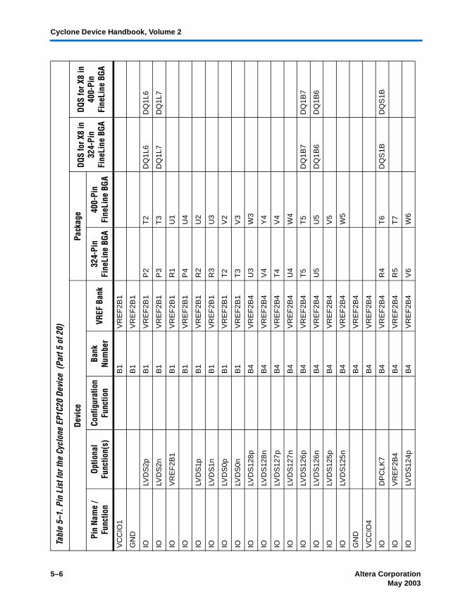
Cyclone Device Handbook, Volume 2
VC
CIO
1B
1V
RE
F2B
1
GN
DB
1V
RE
F2B
1
IOLV
DS
2pB
1V
RE
F2B
1P
2T
2D
Q1L
6D
Q1L
6
IOLV
DS
2nB
1V
RE
F2B
1P
3T
3D
Q1L
7D
Q1L
7
IOV
RE
F2B
1B
1V
RE
F2B
1R
1U
1
IOB
1V
RE
F2B
1P
4U
4
IOLV
DS
1pB
1V
RE
F2B
1R
2U
2
IOLV
DS
1nB
1V
RE
F2B
1R
3U
3
IOLV
DS
0pB
1V
RE
F2B
1T
2V
2
IOLV
DS
0nB
1V
RE
F2B
1T
3V
3
IOLV
DS
128p
B4
VR
EF
2B4
U3
W3
IOLV
DS
128n
B4
VR
EF
2B4
V4
Y4
IOLV
DS
127p
B4
VR
EF
2B4
T4
V4
IOLV
DS
127n
B4
VR
EF
2B4
U4
W4
IOLV
DS
126p
B4
VR
EF
2B4
T5
T5
DQ
1B7
DQ
1B7
IOLV
DS
126n
B4
VR
EF
2B4
U5
U5
DQ
1B6
DQ
1B6
IOLV
DS
125p
B4
VR
EF
2B4
V5
IOLV
DS
125n
B4
VR
EF
2B4
W5
GN
DB
4V
RE
F2B
4
VC
CIO
4B
4V
RE
F2B
4
IOD
PC
LK7
B4
VR
EF
2B4
R4
T6
DQ
S1B
DQ
S1B
IOV
RE
F2B
4B
4V
RE
F2B
4R
5T
7
IOLV
DS
124p
B4
VR
EF
2B4
V6
W6
Tabl
e5–
1.Pi
n Li
st fo
r the
Cyc
lone
EP1
C20
Devi
ce (
Part
5of
20)
Devi
cePa
ckag
eDQ
S fo
r X8
in
324-
Pin
Fine
Line
BGA
DQS
for X
8 in
40
0-Pi
n Fi
neLi
neBG
APi
n Na
me
/ Fu
nctio
nO
ptio
nal
Func
tion(
s)Co
nfig
urat
ion
Func
tion
Bank
Nu
mbe
rVR
EF B
ank
324-
Pin
Fine
Line
BGA
400-
Pin
Fine
Line
BGA
5–6 Altera CorporationPreliminary May 2003

Pin List
IOLV
DS
124n
B4
VR
EF
2B4
U6
Y6
DQ
1B5
DQ
1B5
IOLV
DS
123p
B4
VR
EF
2B4
P6
U6
DQ
1B4
DQ
1B4
IOLV
DS
123n
B4
VR
EF
2B4
P7
V6
IOLV
DS
122p
B4
VR
EF
2B4
T6
W7
IOLV
DS
122n
B4
VR
EF
2B4
R6
Y7
IOLV
DS
121p
B4
VR
EF
2B4
U7
R7
DQ
1B3
DQ
1B3
IOLV
DS
121n
B4
VR
EF
2B4
V7
T8
DQ
1B2
DQ
1B2
IOLV
DS
120p
B4
VR
EF
2B4
T7
V7
DQ
1B1
DQ
1B1
IOLV
DS
120n
B4
VR
EF
2B4
R7
U7
DQ
1B0
DQ
1B0
IOLV
DS
119p
B4
VR
EF
1B4
U8
V8
IOLV
DS
119n
B4
VR
EF
1B4
V8
U8
IOLV
DS
118p
B4
VR
EF
1B4
T8
W8
IOLV
DS
118n
B4
VR
EF
1B4
R8
Y8
GN
DB
4V
RE
F1B
4
VC
CIO
4B
4V
RE
F1B
4
IOLV
DS
117p
B4
VR
EF
1B4
U9
U9
IOLV
DS
117n
B4
VR
EF
1B4
V9
V9
IOLV
DS
116p
B4
VR
EF
1B4
R9
T9
DM
1BD
M1B
IOLV
DS
116n
B4
VR
EF
1B4
T9
R9
IOLV
DS
115p
B4
VR
EF
1B4
Y9
IOLV
DS
115n
B4
VR
EF
1B4
W9
IOLV
DS
114p
B4
VR
EF
1B4
T10
IOLV
DS
114n
B4
VR
EF
1B4
U10
Tabl
e5–
1.Pi
n Li
st fo
r the
Cyc
lone
EP1
C20
Devi
ce (
Part
6of
20)
Devi
cePa
ckag
eDQ
S fo
r X8
in
324-
Pin
Fine
Line
BGA
DQS
for X
8 in
40
0-Pi
n Fi
neLi
neBG
APi
n Na
me
/ Fu
nctio
nO
ptio
nal
Func
tion(
s)Co
nfig
urat
ion
Func
tion
Bank
Nu
mbe
rVR
EF B
ank
324-
Pin
Fine
Line
BGA
400-
Pin
Fine
Line
BGA
Altera Corporation 5–7May 2003 Preliminary
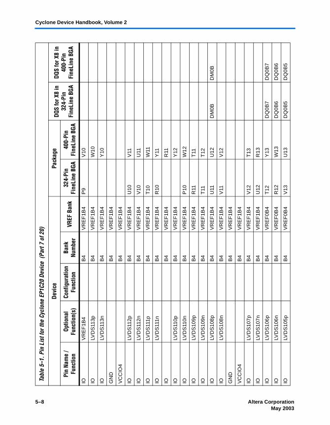
Cyclone Device Handbook, Volume 2
IOV
RE
F1B
4B
4V
RE
F1B
4P
9V
10
IOLV
DS
113p
B4
VR
EF
1B4
W10
IOLV
DS
113n
B4
VR
EF
1B4
Y10
GN
DB
4V
RE
F1B
4
VC
CIO
4B
4V
RE
F1B
4
IOLV
DS
112p
B4
VR
EF
1B4
U10
V11
IOLV
DS
112n
B4
VR
EF
1B4
V10
U11
IOLV
DS
111p
B4
VR
EF
1B4
T10
W11
IOLV
DS
111n
B4
VR
EF
1B4
R10
Y11
IOB
4V
RE
F1B
4R
11
IOLV
DS
110p
B4
VR
EF
1B4
Y12
IOLV
DS
110n
B4
VR
EF
1B4
P10
W12
IOLV
DS
109p
B4
VR
EF
1B4
R11
T11
IOLV
DS
109n
B4
VR
EF
1B4
T11
T12
IOLV
DS
108p
B4
VR
EF
1B4
U11
U12
DM
0BD
M0B
IOLV
DS
108n
B4
VR
EF
1B4
V11
V12
GN
DB
4V
RE
F1B
4
VC
CIO
4B
4V
RE
F1B
4
IOLV
DS
107p
B4
VR
EF
1B4
V12
T13
IOLV
DS
107n
B4
VR
EF
1B4
U12
R13
IOLV
DS
106p
B4
VR
EF
0B4
T12
Y13
DQ
0B7
DQ
0B7
IOLV
DS
106n
B4
VR
EF
0B4
R12
W13
DQ
0B6
DQ
0B6
IOLV
DS
105p
B4
VR
EF
0B4
V13
U13
DQ
0B5
DQ
0B5
Tabl
e5–
1.Pi
n Li
st fo
r the
Cyc
lone
EP1
C20
Devi
ce (
Part
7of
20)
Devi
cePa
ckag
eDQ
S fo
r X8
in
324-
Pin
Fine
Line
BGA
DQS
for X
8 in
40
0-Pi
n Fi
neLi
neBG
APi
n Na
me
/ Fu
nctio
nO
ptio
nal
Func
tion(
s)Co
nfig
urat
ion
Func
tion
Bank
Nu
mbe
rVR
EF B
ank
324-
Pin
Fine
Line
BGA
400-
Pin
Fine
Line
BGA
5–8 Altera CorporationPreliminary May 2003

Pin List
IOLV
DS
105n
B4
VR
EF
0B4
U13
V13
DQ
0B4
DQ
0B4
IOLV
DS
104p
B4
VR
EF
0B4
T13
R14
IOLV
DS
104n
B4
VR
EF
0B4
R13
T14
IOLV
DS
103p
B4
VR
EF
0B4
W14
IOLV
DS
103n
B4
VR
EF
0B4
Y14
IOLV
DS
102p
B4
VR
EF
0B4
U14
IOLV
DS
102n
B4
VR
EF
0B4
V14
IOLV
DS
101p
B4
VR
EF
0B4
V15
IOLV
DS
101n
B4
VR
EF
0B4
P12
U15
IOV
RE
F0B
4B
4V
RE
F0B
4P
13Y
15
IOD
PC
LK6
B4
VR
EF
0B4
U14
W15
DQ
S0B
DQ
S0B
GN
DB
4V
RE
F0B
4
VC
CIO
4B
4V
RE
F0B
4
IOLV
DS
100p
B4
VR
EF
0B4
T15
IOLV
DS
100n
B4
VR
EF
0B4
T16
IOLV
DS
99p
B4
VR
EF
0B4
T14
W16
DQ
0B3
DQ
0B3
IOLV
DS
99n
B4
VR
EF
0B4
R14
V16
DQ
0B2
DQ
0B2
IOLV
DS
98p
B4
VR
EF
0B4
V15
V17
DQ
0B1
DQ
0B1
IOLV
DS
98n
B4
VR
EF
0B4
U15
U16
DQ
0B0
DQ
0B0
IOLV
DS
97p
B4
VR
EF
0B4
U16
Y17
IOLV
DS
97n
B4
VR
EF
0B4
T15
W17
IOLV
DS
96n
B3
VR
EF
2B3
T16
W18
IOLV
DS
96p
B3
VR
EF
2B3
T17
V18
Tabl
e5–
1.Pi
n Li
st fo
r the
Cyc
lone
EP1
C20
Devi
ce (
Part
8of
20)
Devi
cePa
ckag
eDQ
S fo
r X8
in
324-
Pin
Fine
Line
BGA
DQS
for X
8 in
40
0-Pi
n Fi
neLi
neBG
APi
n Na
me
/ Fu
nctio
nO
ptio
nal
Func
tion(
s)Co
nfig
urat
ion
Func
tion
Bank
Nu
mbe
rVR
EF B
ank
324-
Pin
Fine
Line
BGA
400-
Pin
Fine
Line
BGA
Altera Corporation 5–9May 2003 Preliminary

Cyclone Device Handbook, Volume 2
IOLV
DS
95n
B3
VR
EF
2B3
R17
V19
IOLV
DS
95p
B3
VR
EF
2B3
R18
U20
IOLV
DS
94n
B3
VR
EF
2B3
R15
U18
DQ
1R7
DQ
1R7
IOLV
DS
94p
B3
VR
EF
2B3
R16
U19
IOV
RE
F2B
3B
3V
RE
F2B
3P
16U
17
IOB
3V
RE
F2B
3P
17T
18D
Q1R
6D
Q1R
6
GN
DB
3V
RE
F2B
3
VC
CIO
3B
3V
RE
F2B
3
IOD
PC
LK5
B3
VR
EF
2B3
P15
T19
DQ
S1R
DQ
S1R
IOLV
DS
93n
B3
VR
EF
2B3
P14
T17
DQ
1R5
DQ
1R5
IOLV
DS
93p
B3
VR
EF
2B3
N14
R16
DQ
1R4
DQ
1R4
IOLV
DS
92n
B3
VR
EF
2B3
N18
R19
IOLV
DS
92p
B3
VR
EF
2B3
N17
R20
IOLV
DS
91n
B3
VR
EF
2B3
N13
R17
IOLV
DS
91p
B3
VR
EF
2B3
N12
R18
IOLV
DS
90n
B3
VR
EF
2B3
N16
R15
IOLV
DS
90p
B3
VR
EF
2B3
N15
P14
IOLV
DS
89n
B3
VR
EF
2B3
M18
P18
IOLV
DS
89p
B3
VR
EF
2B3
M17
P17
DQ
1R3
DQ
1R3
IOLV
DS
88n
B3
VR
EF
2B3
M14
P16
DQ
1R2
DQ
1R2
IOLV
DS
88p
B3
VR
EF
2B3
M15
P15
DQ
1R1
DQ
1R1
IOLV
DS
87n
B3
VR
EF
2B3
P19
IOLV
DS
87p
B3
VR
EF
2B3
P20
Tabl
e5–
1.Pi
n Li
st fo
r the
Cyc
lone
EP1
C20
Devi
ce (
Part
9of
20)
Devi
cePa
ckag
eDQ
S fo
r X8
in
324-
Pin
Fine
Line
BGA
DQS
for X
8 in
40
0-Pi
n Fi
neLi
neBG
APi
n Na
me
/ Fu
nctio
nO
ptio
nal
Func
tion(
s)Co
nfig
urat
ion
Func
tion
Bank
Nu
mbe
rVR
EF B
ank
324-
Pin
Fine
Line
BGA
400-
Pin
Fine
Line
BGA
5–10 Altera CorporationPreliminary May 2003

Pin List
IOB
3V
RE
F2B
3M
16N
14D
Q1R
0D
Q1R
0
GN
DB
3V
RE
F2B
3
VC
CIO
3B
3V
RE
F2B
3
IOLV
DS
86n
B3
VR
EF
1B3
L18
N18
IOLV
DS
86p
B3
VR
EF
1B3
L17
N17
IOLV
DS
85n
B3
VR
EF
1B3
M13
N19
IOLV
DS
85p
B3
VR
EF
1B3
L13
N20
IOLV
DS
84n
B3
VR
EF
1B3
L16
N16
DM
1RD
M1R
IOLV
DS
84p
B3
VR
EF
1B3
L15
N15
IOLV
DS
83n
B3
VR
EF
1B3
M18
IOLV
DS
83p
B3
VR
EF
1B3
M17
IOLV
DS
82n
B3
VR
EF
1B3
M15
IOLV
DS
82p
B3
VR
EF
1B3
M16
IOLV
DS
81n
B3
VR
EF
1B3
M20
IOLV
DS
81p
B3
VR
EF
1B3
M19
IOB
3V
RE
F1B
3L1
4M
14
IOP
LL2_
OU
Tn
B3
VR
EF
1B3
K16
M13
IOP
LL2_
OU
Tp
B3
VR
EF
1B3
K15
L13
CO
NF
_DO
NE
CO
NF
_DO
NE
B3
VR
EF
1B3
K17
L18
nSTA
TU
SnS
TAT
US
B3
VR
EF
1B3
L12
L17
TC
KT
CK
B3
VR
EF
1B3
K18
L19
TM
ST
MS
B3
VR
EF
1B3
K14
L16
TD
OT
DO
B3
VR
EF
1B3
K13
L20
Tabl
e5–
1.Pi
n Li
st fo
r the
Cyc
lone
EP1
C20
Devi
ce (
Part
10of
20)
Devi
cePa
ckag
eDQ
S fo
r X8
in
324-
Pin
Fine
Line
BGA
DQS
for X
8 in
40
0-Pi
n Fi
neLi
neBG
APi
n Na
me
/ Fu
nctio
nO
ptio
nal
Func
tion(
s)Co
nfig
urat
ion
Func
tion
Bank
Nu
mbe
rVR
EF B
ank
324-
Pin
Fine
Line
BGA
400-
Pin
Fine
Line
BGA
Altera Corporation 5–11May 2003 Preliminary
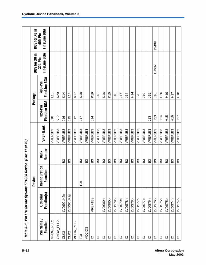
Cyclone Device Handbook, Volume 2
GN
DG
_PLL
2V
RE
F1B
3J1
8L1
5
GN
DA
_PLL
2V
RE
F1B
3K
12K
20
CLK
3LV
DS
CLK
2nB
3V
RE
F1B
3J1
6K
14
CLK
2LV
DS
CLK
2pB
3V
RE
F1B
3J1
5L1
4
VC
CA
_PLL
2V
RE
F1B
3J1
2K
17
TD
IT
DI
B3
VR
EF
1B3
J17
K18
VC
CIO
3B
3V
RE
F1B
3
IOV
RE
F1B
3B
3V
RE
F1B
3J1
4K
19
IOB
3V
RE
F1B
3J1
3
IOLV
DS
80n
B3
VR
EF
1B3
K16
IOLV
DS
80p
B3
VR
EF
1B3
K15
IOLV
DS
79n
B3
VR
EF
1B3
J18
IOLV
DS
79p
B3
VR
EF
1B3
J17
IOLV
DS
78n
B3
VR
EF
1B3
J14
IOLV
DS
78p
B3
VR
EF
1B3
H14
IOLV
DS
77n
B3
VR
EF
1B3
J20
IOLV
DS
77p
B3
VR
EF
1B3
J19
IOLV
DS
76n
B3
VR
EF
1B3
J13
J15
IOLV
DS
76p
B3
VR
EF
1B3
H13
J16
DM
0RD
M0R
IOLV
DS
75n
B3
VR
EF
1B3
H14
H20
IOLV
DS
75p
B3
VR
EF
1B3
H15
H19
IOLV
DS
74n
B3
VR
EF
1B3
H16
H17
IOLV
DS
74p
B3
VR
EF
1B3
H17
H18
Tabl
e5–
1.Pi
n Li
st fo
r the
Cyc
lone
EP1
C20
Devi
ce (
Part
11of
20)
Devi
cePa
ckag
eDQ
S fo
r X8
in
324-
Pin
Fine
Line
BGA
DQS
for X
8 in
40
0-Pi
n Fi
neLi
neBG
APi
n Na
me
/ Fu
nctio
nO
ptio
nal
Func
tion(
s)Co
nfig
urat
ion
Func
tion
Bank
Nu
mbe
rVR
EF B
ank
324-
Pin
Fine
Line
BGA
400-
Pin
Fine
Line
BGA
5–12 Altera CorporationPreliminary May 2003

Pin List
GN
DB
3V
RE
F0B
3
VC
CIO
3B
3V
RE
F0B
3
IOB
3V
RE
F0B
3H
18H
16D
Q0R
7D
Q0R
7
IOLV
DS
73n
B3
VR
EF
0B3
G18
G17
DQ
0R6
DQ
0R6
IOLV
DS
73p
B3
VR
EF
0B3
G17
G18
DQ
0R5
DQ
0R5
IOLV
DS
72n
B3
VR
EF
0B3
G13
H15
DQ
0R4
DQ
0R4
IOLV
DS
72p
B3
VR
EF
0B3
G14
G14
IOLV
DS
71n
B3
VR
EF
0B3
G15
G19
IOLV
DS
71p
B3
VR
EF
0B3
G16
G20
IOLV
DS
70n
B3
VR
EF
0B3
G12
G15
IOLV
DS
70p
B3
VR
EF
0B3
F12
G16
IOLV
DS
69n
B3
VR
EF
0B3
F18
F20
IOLV
DS
69p
B3
VR
EF
0B3
F17
F19
IOLV
DS
68n
B3
VR
EF
0B3
F13
F15
IOLV
DS
68p
B3
VR
EF
0B3
F14
F16
IOLV
DS
67n
B3
VR
EF
0B3
F16
E19
IOLV
DS
67p
B3
VR
EF
0B3
F15
E18
DQ
0R3
DQ
0R3
IOD
PC
LK4
B3
VR
EF
0B3
E17
F18
DQ
S0R
DQ
S0R
GN
DB
3V
RE
F0B
3
VC
CIO
3B
3V
RE
F0B
3
IOLV
DS
66n
B3
VR
EF
0B3
E16
F17
DQ
0R2
DQ
0R2
IOLV
DS
66p
B3
VR
EF
0B3
E15
E17
DQ
0R1
DQ
0R1
IOB
3V
RE
F0B
3D
18D
20D
Q0R
0D
Q0R
0
Tabl
e5–
1.Pi
n Li
st fo
r the
Cyc
lone
EP1
C20
Devi
ce (
Part
12of
20)
Devi
cePa
ckag
eDQ
S fo
r X8
in
324-
Pin
Fine
Line
BGA
DQS
for X
8 in
40
0-Pi
n Fi
neLi
neBG
APi
n Na
me
/ Fu
nctio
nO
ptio
nal
Func
tion(
s)Co
nfig
urat
ion
Func
tion
Bank
Nu
mbe
rVR
EF B
ank
324-
Pin
Fine
Line
BGA
400-
Pin
Fine
Line
BGA
Altera Corporation 5–13May 2003 Preliminary
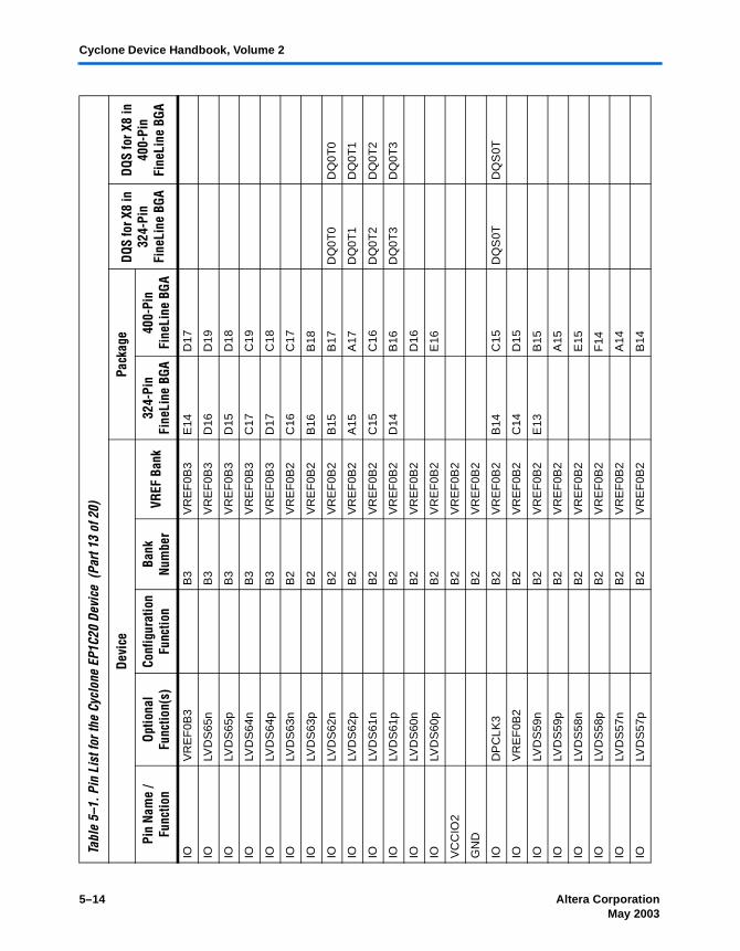
Cyclone Device Handbook, Volume 2
IOV
RE
F0B
3B
3V
RE
F0B
3E
14D
17
IOLV
DS
65n
B3
VR
EF
0B3
D16
D19
IOLV
DS
65p
B3
VR
EF
0B3
D15
D18
IOLV
DS
64n
B3
VR
EF
0B3
C17
C19
IOLV
DS
64p
B3
VR
EF
0B3
D17
C18
IOLV
DS
63n
B2
VR
EF
0B2
C16
C17
IOLV
DS
63p
B2
VR
EF
0B2
B16
B18
IOLV
DS
62n
B2
VR
EF
0B2
B15
B17
DQ
0T0
DQ
0T0
IOLV
DS
62p
B2
VR
EF
0B2
A15
A17
DQ
0T1
DQ
0T1
IOLV
DS
61n
B2
VR
EF
0B2
C15
C16
DQ
0T2
DQ
0T2
IOLV
DS
61p
B2
VR
EF
0B2
D14
B16
DQ
0T3
DQ
0T3
IOLV
DS
60n
B2
VR
EF
0B2
D16
IOLV
DS
60p
B2
VR
EF
0B2
E16
VC
CIO
2B
2V
RE
F0B
2
GN
DB
2V
RE
F0B
2
IOD
PC
LK3
B2
VR
EF
0B2
B14
C15
DQ
S0T
DQ
S0T
IOV
RE
F0B
2B
2V
RE
F0B
2C
14D
15
IOLV
DS
59n
B2
VR
EF
0B2
E13
B15
IOLV
DS
59p
B2
VR
EF
0B2
A15
IOLV
DS
58n
B2
VR
EF
0B2
E15
IOLV
DS
58p
B2
VR
EF
0B2
F14
IOLV
DS
57n
B2
VR
EF
0B2
A14
IOLV
DS
57p
B2
VR
EF
0B2
B14
Tabl
e5–
1.Pi
n Li
st fo
r the
Cyc
lone
EP1
C20
Devi
ce (
Part
13of
20)
Devi
cePa
ckag
eDQ
S fo
r X8
in
324-
Pin
Fine
Line
BGA
DQS
for X
8 in
40
0-Pi
n Fi
neLi
neBG
APi
n Na
me
/ Fu
nctio
nO
ptio
nal
Func
tion(
s)Co
nfig
urat
ion
Func
tion
Bank
Nu
mbe
rVR
EF B
ank
324-
Pin
Fine
Line
BGA
400-
Pin
Fine
Line
BGA
5–14 Altera CorporationPreliminary May 2003
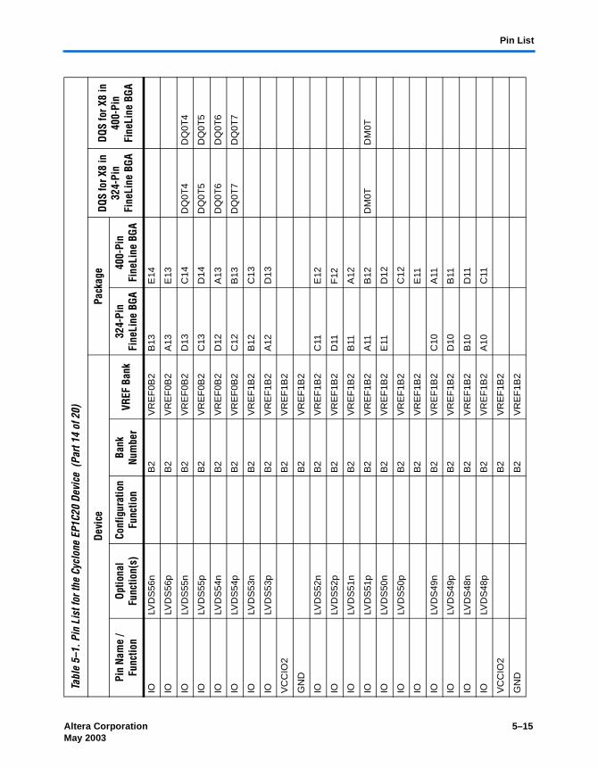
Pin List
IOLV
DS
56n
B2
VR
EF
0B2
B13
E14
IOLV
DS
56p
B2
VR
EF
0B2
A13
E13
IOLV
DS
55n
B2
VR
EF
0B2
D13
C14
DQ
0T4
DQ
0T4
IOLV
DS
55p
B2
VR
EF
0B2
C13
D14
DQ
0T5
DQ
0T5
IOLV
DS
54n
B2
VR
EF
0B2
D12
A13
DQ
0T6
DQ
0T6
IOLV
DS
54p
B2
VR
EF
0B2
C12
B13
DQ
0T7
DQ
0T7
IOLV
DS
53n
B2
VR
EF
1B2
B12
C13
IOLV
DS
53p
B2
VR
EF
1B2
A12
D13
VC
CIO
2B
2V
RE
F1B
2
GN
DB
2V
RE
F1B
2
IOLV
DS
52n
B2
VR
EF
1B2
C11
E12
IOLV
DS
52p
B2
VR
EF
1B2
D11
F12
IOLV
DS
51n
B2
VR
EF
1B2
B11
A12
IOLV
DS
51p
B2
VR
EF
1B2
A11
B12
DM
0TD
M0T
IOLV
DS
50n
B2
VR
EF
1B2
E11
D12
IOLV
DS
50p
B2
VR
EF
1B2
C12
IOB
2V
RE
F1B
2E
11
IOLV
DS
49n
B2
VR
EF
1B2
C10
A11
IOLV
DS
49p
B2
VR
EF
1B2
D10
B11
IOLV
DS
48n
B2
VR
EF
1B2
B10
D11
IOLV
DS
48p
B2
VR
EF
1B2
A10
C11
VC
CIO
2B
2V
RE
F1B
2
GN
DB
2V
RE
F1B
2
Tabl
e5–
1.Pi
n Li
st fo
r the
Cyc
lone
EP1
C20
Devi
ce (
Part
14of
20)
Devi
cePa
ckag
eDQ
S fo
r X8
in
324-
Pin
Fine
Line
BGA
DQS
for X
8 in
40
0-Pi
n Fi
neLi
neBG
APi
n Na
me
/ Fu
nctio
nO
ptio
nal
Func
tion(
s)Co
nfig
urat
ion
Func
tion
Bank
Nu
mbe
rVR
EF B
ank
324-
Pin
Fine
Line
BGA
400-
Pin
Fine
Line
BGA
Altera Corporation 5–15May 2003 Preliminary

Cyclone Device Handbook, Volume 2
IOLV
DS
47n
B2
VR
EF
1B2
D10
IOLV
DS
47p
B2
VR
EF
1B2
C10
IOV
RE
F1B
2B
2V
RE
F1B
2E
10F
10
IOLV
DS
46n
B2
VR
EF
1B2
A10
IOLV
DS
46p
B2
VR
EF
1B2
B10
IOLV
DS
45n
B2
VR
EF
1B2
E10
IOLV
DS
45p
B2
VR
EF
1B2
E9
IOLV
DS
44n
B2
VR
EF
1B2
D9
C9
DM
1TD
M1T
IOLV
DS
44p
B2
VR
EF
1B2
C9
D9
IOLV
DS
43n
B2
VR
EF
1B2
A9
A9
IOLV
DS
43p
B2
VR
EF
1B2
B9
B9
VC
CIO
2B
2V
RE
F1B
2
GN
DB
2V
RE
F1B
2
IOLV
DS
42n
B2
VR
EF
1B2
D8
C8
IOLV
DS
42p
B2
VR
EF
1B2
C8
D8
IOLV
DS
41n
B2
VR
EF
1B2
A8
A8
IOLV
DS
41p
B2
VR
EF
1B2
B8
B8
IOLV
DS
40n
B2
VR
EF
2B2
E8
E8
DQ
1T0
DQ
1T0
IOLV
DS
40p
B2
VR
EF
2B2
E7
F8
DQ
1T1
DQ
1T1
IOLV
DS
39n
B2
VR
EF
2B2
A7
C7
DQ
1T2
DQ
1T2
IOLV
DS
39p
B2
VR
EF
2B2
B7
D7
DQ
1T3
DQ
1T3
IOLV
DS
38n
B2
VR
EF
2B2
D7
A7
IOLV
DS
38p
B2
VR
EF
2B2
C7
B7
Tabl
e5–
1.Pi
n Li
st fo
r the
Cyc
lone
EP1
C20
Devi
ce (
Part
15of
20)
Devi
cePa
ckag
eDQ
S fo
r X8
in
324-
Pin
Fine
Line
BGA
DQS
for X
8 in
40
0-Pi
n Fi
neLi
neBG
APi
n Na
me
/ Fu
nctio
nO
ptio
nal
Func
tion(
s)Co
nfig
urat
ion
Func
tion
Bank
Nu
mbe
rVR
EF B
ank
324-
Pin
Fine
Line
BGA
400-
Pin
Fine
Line
BGA
5–16 Altera CorporationPreliminary May 2003

Pin List
IOLV
DS
37n
B2
VR
EF
2B2
E6
E7
IOLV
DS
37p
B2
VR
EF
2B2
D6
F7
IOLV
DS
36n
B2
VR
EF
2B2
B6
A6
IOLV
DS
36p
B2
VR
EF
2B2
C6
B6
IOV
RE
F2B
2B
2V
RE
F2B
2A
6E
6
IOD
PC
LK2
B2
VR
EF
2B2
B5
C6
DQ
S1T
DQ
S1T
VC
CIO
2B
2V
RE
F2B
2
GN
DB
2V
RE
F2B
2
IOLV
DS
35n
B2
VR
EF
2B2
B5
IOLV
DS
35p
B2
VR
EF
2B2
C5
IOLV
DS
34n
B2
VR
EF
2B2
C5
D6
DQ
1T4
DQ
1T4
IOLV
DS
34p
B2
VR
EF
2B2
D5
D5
DQ
1T5
DQ
1T5
IOLV
DS
33n
B2
VR
EF
2B2
A4
A4
DQ
1T6
DQ
1T6
IOLV
DS
33p
B2
VR
EF
2B2
B4
B4
DQ
1T7
DQ
1T7
IOLV
DS
32n
DE
V_O
EB
2V
RE
F2B
2B
3B
3
IOLV
DS
32p
DE
V_C
LRn
B2
VR
EF
2B2
C4
C4
VC
CIN
TA
17A
19
VC
CIN
TA
2A
2
VC
CIN
TB
1B
1
VC
CIN
TB
18B
20
VC
CIN
TF
10H
10
VC
CIN
TF
8H
12
VC
CIN
TG
11J1
1
Tabl
e5–
1.Pi
n Li
st fo
r the
Cyc
lone
EP1
C20
Devi
ce (
Part
16of
20)
Devi
cePa
ckag
eDQ
S fo
r X8
in
324-
Pin
Fine
Line
BGA
DQS
for X
8 in
40
0-Pi
n Fi
neLi
neBG
APi
n Na
me
/ Fu
nctio
nO
ptio
nal
Func
tion(
s)Co
nfig
urat
ion
Func
tion
Bank
Nu
mbe
rVR
EF B
ank
324-
Pin
Fine
Line
BGA
400-
Pin
Fine
Line
BGA
Altera Corporation 5–17May 2003 Preliminary

Cyclone Device Handbook, Volume 2
VC
CIN
TG
9J9
VC
CIN
TH
10K
10
VC
CIN
TJ9
K12
VC
CIN
TK
10L1
1
VC
CIN
TL9
L9
VC
CIN
TM
10M
10
VC
CIN
TM
8M
12
VC
CIN
TN
11N
11
VC
CIN
TN
9N
9
VC
CIN
TU
1W
1
VC
CIN
TU
18W
20
VC
CIN
TV
17Y
19
VC
CIN
TV
2Y
2
VC
CIO
1E
1
VC
CIO
1E
1H
8
VC
CIO
1G
7K
8
VC
CIO
1M
7N
8
VC
CIO
1P
1T
1
VC
CIO
4R
10
VC
CIO
4P
11R
12
VC
CIO
4P
8R
8
VC
CIO
4V
14Y
16
VC
CIO
4V
5Y
5
Tabl
e5–
1.Pi
n Li
st fo
r the
Cyc
lone
EP1
C20
Devi
ce (
Part
17of
20)
Devi
cePa
ckag
eDQ
S fo
r X8
in
324-
Pin
Fine
Line
BGA
DQS
for X
8 in
40
0-Pi
n Fi
neLi
neBG
APi
n Na
me
/ Fu
nctio
nO
ptio
nal
Func
tion(
s)Co
nfig
urat
ion
Func
tion
Bank
Nu
mbe
rVR
EF B
ank
324-
Pin
Fine
Line
BGA
400-
Pin
Fine
Line
BGA
5–18 Altera CorporationPreliminary May 2003
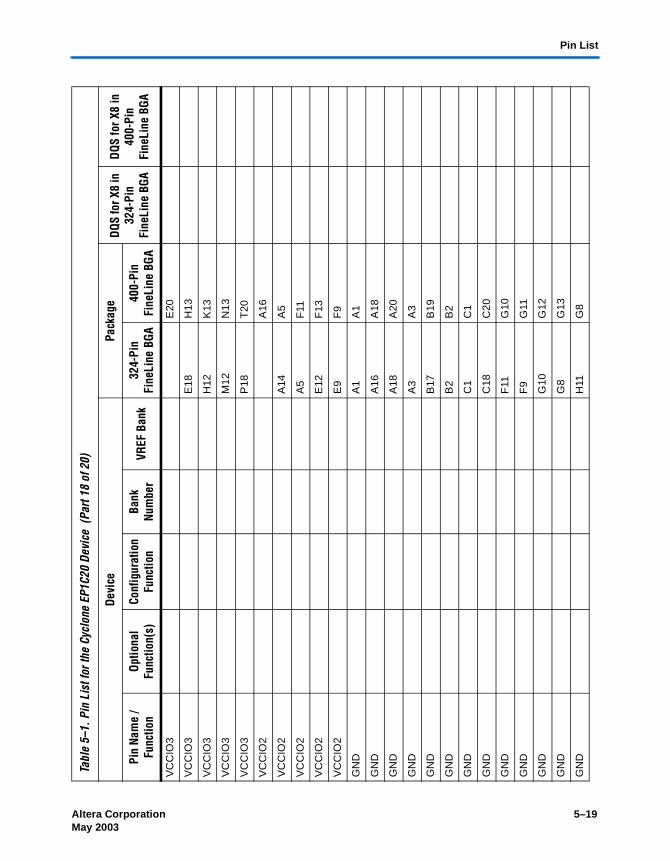
Pin List
VC
CIO
3E
20
VC
CIO
3E
18H
13
VC
CIO
3H
12K
13
VC
CIO
3M
12N
13
VC
CIO
3P
18T
20
VC
CIO
2A
16
VC
CIO
2A
14A
5
VC
CIO
2A
5F
11
VC
CIO
2E
12F
13
VC
CIO
2E
9F
9
GN
DA
1A
1
GN
DA
16A
18
GN
DA
18A
20
GN
DA
3A
3
GN
DB
17B
19
GN
DB
2B
2
GN
DC
1C
1
GN
DC
18C
20
GN
DF
11G
10
GN
DF
9G
11
GN
DG
10G
12
GN
DG
8G
13
GN
DH
11G
8
Tabl
e5–
1.Pi
n Li
st fo
r the
Cyc
lone
EP1
C20
Devi
ce (
Part
18of
20)
Devi
cePa
ckag
eDQ
S fo
r X8
in
324-
Pin
Fine
Line
BGA
DQS
for X
8 in
40
0-Pi
n Fi
neLi
neBG
APi
n Na
me
/ Fu
nctio
nO
ptio
nal
Func
tion(
s)Co
nfig
urat
ion
Func
tion
Bank
Nu
mbe
rVR
EF B
ank
324-
Pin
Fine
Line
BGA
400-
Pin
Fine
Line
BGA
Altera Corporation 5–19May 2003 Preliminary

Cyclone Device Handbook, Volume 2
GN
DH
8G
9
GN
DH
9H
11
GN
DJ1
0H
9
GN
DJ1
1J1
0
GN
DJ8
J12
GN
DK
11K
11
GN
DK
8K
9
GN
DK
9L1
0
GN
DL1
0L1
2
GN
DL1
1M
11
GN
DL8
M9
GN
DM
11N
10
GN
DM
9N
12
GN
DN
10P
10
GN
DN
8P
11
GN
DT
1P
12
GN
DT
18P
13
GN
DU
17P
8
GN
DU
2P
9
GN
DV
1V
1
GN
DV
16V
20
GN
DV
18W
19
GN
DV
3W
2
Tabl
e5–
1.Pi
n Li
st fo
r the
Cyc
lone
EP1
C20
Devi
ce (
Part
19of
20)
Devi
cePa
ckag
eDQ
S fo
r X8
in
324-
Pin
Fine
Line
BGA
DQS
for X
8 in
40
0-Pi
n Fi
neLi
neBG
APi
n Na
me
/ Fu
nctio
nO
ptio
nal
Func
tion(
s)Co
nfig
urat
ion
Func
tion
Bank
Nu
mbe
rVR
EF B
ank
324-
Pin
Fine
Line
BGA
400-
Pin
Fine
Line
BGA
5–20 Altera CorporationPreliminary May 2003

Pin List
GN
DY
1
GN
DY
18
GN
DY
20
GN
DY
3
Tabl
e5–
1.Pi
n Li
st fo
r the
Cyc
lone
EP1
C20
Devi
ce (
Part
20of
20)
Devi
cePa
ckag
eDQ
S fo
r X8
in
324-
Pin
Fine
Line
BGA
DQS
for X
8 in
40
0-Pi
n Fi
neLi
neBG
APi
n Na
me
/ Fu
nctio
nO
ptio
nal
Func
tion(
s)Co
nfig
urat
ion
Func
tion
Bank
Nu
mbe
rVR
EF B
ank
324-
Pin
Fine
Line
BGA
400-
Pin
Fine
Line
BGA
Altera Corporation 5–21May 2003 Preliminary

Cyclone Device Handbook, Volume 2
Pin
Defin
ition
sTa
ble
5–2
show
s th
e pi
n d
efin
itio
ns fo
r th
e E
P1C
20 d
evic
e.
Tabl
e5–
2.Pi
n De
finiti
ons
for t
he E
P1C2
0 De
vice
(Pa
rt1
of4)
Pin
Nam
ePi
n Ty
pe (1
st, 2
nd,
& 3
rd F
unct
ion)
Pin
Desc
riptio
n
Supp
ly a
nd R
efer
ence
Pin
s
VC
CIO
[1..4
]P
ower
The
se a
re I/
O s
uppl
y vo
ltage
pin
s fo
r ban
ks 1
thro
ugh
4. E
ach
bank
can
sup
port
a d
iffer
ent v
olta
ge le
vel.
VC
CIO
sup
plie
s po
wer
to th
e ou
tput
buf
fers
for a
ll I/O
sta
ndar
ds. V
CC
IO a
lso
supp
lies
pow
er to
the
inpu
t bu
ffers
use
d fo
r th
e LV
TT
L, L
VC
MO
S, 1
.5-V
, 1.8
-V, 2
.5-V
, and
3.3
-V P
CI I
/O s
tand
ards
.
VC
CIN
TP
ower
The
se a
re in
tern
al lo
gic
arra
y vo
ltage
sup
ply
pins
. VC
CIN
T a
lso
supp
lies
pow
er to
the
inpu
t buf
fers
use
d fo
r th
e LV
DS
, SS
TL2
, and
SS
TL3
I/O
sta
ndar
ds.
VR
EF
[0..2
]B[1
..4]
I/O, I
nput
Inpu
t ref
eren
ce v
olta
ge fo
r ban
ks 1
-4. I
f a b
ank
uses
a v
olta
ge-r
efer
ence
d I/O
sta
ndar
d, th
en th
ese
pins
ar
e us
ed a
s th
e vo
ltage
-ref
eren
ce p
ins
for
the
bank
. If v
olta
ge r
efer
ence
I/O
sta
ndar
ds a
re n
ot u
sed
in
the
bank
, the
VR
EF
pin
s ar
e av
aila
ble
as u
ser
I/O p
ins.
VC
CA
_PLL
[1..2
]P
ower
Ana
log
pow
er fo
r P
LLs[
1..2
]. T
he d
esig
ner
mus
t con
nect
this
pin
to 1
.5 V
, eve
n if
the
PLL
is n
ot u
sed.
GN
DA
_PLL
[1..2
]G
roun
dA
nalo
g gr
ound
for
PLL
s[1.
.2].
The
des
igne
r ca
n co
nnec
t thi
s pi
n to
the
GN
D p
lane
on
the
boar
d.
GN
DG
_PLL
[1..2
]G
roun
dG
uard
rin
g gr
ound
for
PLL
s[1.
.2].
The
des
igne
r ca
n co
nnec
t thi
s pi
n to
the
GN
D p
lane
on
the
boar
d.
Conf
igur
atio
n an
d JT
AG P
ins
CO
NF
_DO
NE
Bid
irect
iona
l (op
en-
drai
n)T
his
is a
ded
icat
ed c
onfig
urat
ion
stat
us p
in; i
t is
not a
vaila
ble
as a
use
r I/O
pin
.
nSTA
TU
SB
idire
ctio
nal (
open
-dr
ain)
Thi
s is
a d
edic
ated
con
figur
atio
n st
atus
pin
; it i
s no
t ava
ilabl
e as
a u
ser
I/O p
in.
nCO
NF
IGIn
put
Ded
icat
ed c
onfig
urat
ion
cont
rol i
nput
. A lo
w tr
ansi
tion
rese
ts th
e ta
rget
dev
ice;
a lo
w-t
o-hi
gh tr
ansi
tion
begi
ns c
onfig
urat
ion.
All
I/O p
ins
tri-s
tate
whe
n nC
ON
FIG
is d
riven
low
.
DC
LKIn
put (
PS
mod
e),
Out
put (
AS
mod
e)In
pas
sive
ser
ial c
onfig
urat
ion
mod
e, D
CLK
is a
clo
ck in
put u
sed
to c
lock
con
figur
atio
n da
ta fr
om a
n ex
tern
al s
ourc
e in
to th
e C
yclo
ne d
evic
e. In
act
ive
seria
l con
figur
atio
n m
ode,
DC
LK is
a c
lock
out
put f
rom
th
e C
yclo
ne d
evic
e (t
he C
yclo
ne d
evic
e ac
ts a
s m
aste
r in
this
mod
e). T
his
is a
ded
icat
ed p
in u
sed
for
conf
igur
atio
n.
DA
TA0
Inpu
tD
edic
ated
con
figur
atio
n da
ta in
put p
in.
5–22 Altera CorporationPreliminary May 2003

Pin Definitions
nCE
Inpu
tA
ctiv
e-lo
w c
hip
enab
le. D
edic
ated
chi
p en
able
inpu
t use
d to
det
ect w
hich
dev
ice
is a
ctiv
e in
a c
hain
of
devi
ces.
Whe
n nC
E is
low
, the
dev
ice
is e
nabl
ed. W
hen
nCE
is h
igh,
the
devi
ce is
dis
able
d.
nCE
OO
utpu
tO
utpu
t tha
t driv
es lo
w w
hen
devi
ce c
onfig
urat
ion
is c
ompl
ete.
Dur
ing
mul
ti-de
vice
con
figur
atio
n, th
is p
in
feed
s a
subs
eque
nt d
evic
e’s
nCE
pin
.
AS
DO
I/O, O
utpu
tA
ctiv
e se
rial d
ata
outp
ut fr
om th
e C
yclo
ne d
evic
e. T
his
outp
ut p
in is
util
ized
dur
ing
activ
e se
rial
conf
igur
atio
n m
ode.
The
Cyc
lone
dev
ice
cont
rols
con
figur
atio
n an
d dr
ives
add
ress
and
con
trol
in
form
atio
n ou
t on
AS
DO
. In
pass
ive
seria
l con
figur
atio
n, th
is p
in is
ava
ilabl
e as
a u
ser
I/O p
in.
nCS
OI/O
, Out
put
Chi
p se
lect
out
put t
hat e
nabl
es/d
isab
les
a se
rial c
onfig
urat
ion
devi
ce.
Thi
s ou
tput
is u
tiliz
ed d
urin
g ac
tive
seria
l con
figur
atio
n m
ode.
The
Cyc
lone
dev
ice
cont
rols
con
figur
atio
n an
d en
able
s th
e se
rial
conf
igur
atio
n de
vice
by
driv
ing
nCS
O lo
w. I
n pa
ssiv
e se
rial c
onfig
urat
ion,
this
pin
is a
vaila
ble
as a
use
r I/O
pin
.
INIT
_DO
NE
I/O, O
utpu
t (op
en-
drai
n)T
his
is a
dua
l-pur
pose
pin
and
can
be
used
as
an I/
O p
in w
hen
not e
nabl
ed a
s IN
IT_D
ON
E. W
hen
enab
led,
the
pin
indi
cate
s w
hen
the
devi
ce h
as e
nter
ed u
ser
mod
e. T
his
pin
can
be u
sed
as a
use
r I/O
pi
n af
ter
conf
igur
atio
n.
CLK
US
RI/O
, Inp
utO
ptio
nal u
ser-
supp
lied
cloc
k in
put.
Syn
chro
nize
s th
e in
itial
izat
ion
of o
ne o
r m
ore
devi
ces.
Thi
s pi
n ca
n be
use
d as
a u
ser
I/O p
in a
fter
conf
igur
atio
n.
DE
V_C
LRn
I/O, I
nput
Dua
l-pur
pose
pin
that
can
ove
rrid
e al
l cle
ars
on a
ll de
vice
reg
iste
rs. W
hen
this
pin
is d
riven
low
, all
regi
ster
s ar
e cl
eare
d; w
hen
this
pin
is d
riven
hig
h, a
ll re
gist
ers
beha
ve a
s de
fined
in th
e de
sign
.
DE
V_O
EI/O
, Inp
utD
ual-p
urpo
se p
in th
at c
an o
verr
ide
all t
ri-st
ates
on
the
devi
ce. W
hen
this
pin
is d
riven
low
, all
I/O p
ins
are
tri-s
tate
d; w
hen
this
pin
is d
riven
hig
h, a
ll I/O
pin
s be
have
as
defin
ed in
the
desi
gn.
MS
EL[
1..0
]In
put
Ded
icat
ed m
ode
sele
ct c
ontr
ol p
ins
that
set
the
conf
igur
atio
n m
ode
for
the
devi
ce.
TM
SIn
put
Thi
s is
a d
edic
ated
JTA
G in
put p
in.
TD
IIn
put
Thi
s is
a d
edic
ated
JTA
G in
put p
in.
TC
KIn
put
Thi
s is
a d
edic
ated
JTA
G in
put p
in.
TD
OO
utpu
tT
his
is a
ded
icat
ed J
TAG
out
put p
in.
Tabl
e5–
2.Pi
n De
finiti
ons
for t
he E
P1C2
0 De
vice
(Pa
rt2
of4)
Pin
Nam
ePi
n Ty
pe (1
st, 2
nd,
& 3
rd F
unct
ion)
Pin
Desc
riptio
n
Altera Corporation 5–23May 2003 Preliminary
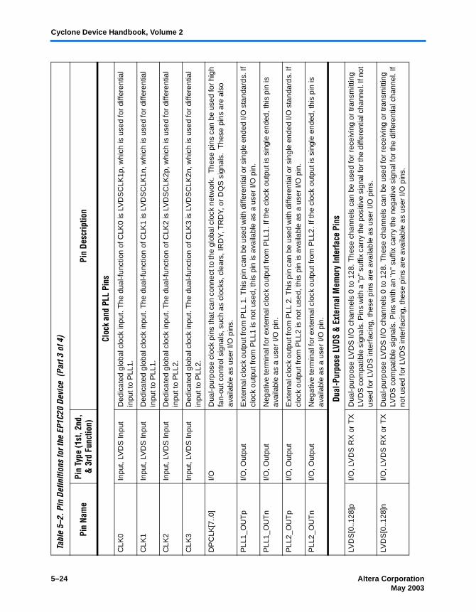
Cyclone Device Handbook, Volume 2
Cloc
k an
d PL
L Pi
ns
CLK
0In
put,
LVD
S In
put
Ded
icat
ed g
loba
l clo
ck in
put.
The
dua
l-fun
ctio
n of
CLK
0 is
LV
DS
CLK
1p, w
hich
is u
sed
for
diffe
rent
ial
inpu
t to
PLL
1.
CLK
1In
put,
LVD
S In
put
Ded
icat
ed g
loba
l clo
ck in
put.
The
dua
l-fun
ctio
n of
CLK
1 is
LV
DS
CLK
1n, w
hich
is u
sed
for
diffe
rent
ial
inpu
t to
PLL
1.
CLK
2In
put,
LVD
S In
put
Ded
icat
ed g
loba
l clo
ck in
put.
The
dua
l-fun
ctio
n of
CLK
2 is
LV
DS
CLK
2p, w
hich
is u
sed
for
diffe
rent
ial
inpu
t to
PLL
2.
CLK
3In
put,
LVD
S In
put
Ded
icat
ed g
loba
l clo
ck in
put.
The
dua
l-fun
ctio
n of
CLK
3 is
LV
DS
CLK
2n, w
hich
is u
sed
for
diffe
rent
ial
inpu
t to
PLL
2.
DP
CLK
[7..0
]I/O
Dua
l-pur
pose
clo
ck p
ins
that
can
con
nect
to th
e gl
obal
clo
ck n
etw
ork.
The
se p
ins
can
be u
sed
for
high
fa
n-ou
t con
trol
sig
nals
, suc
h as
clo
cks,
cle
ars,
IRD
Y, T
RD
Y, o
r D
QS
sig
nals
. T
hese
pin
s ar
e al
so
avai
labl
e as
use
r I/O
pin
s.
PLL
1_O
UT
pI/O
, Out
put
Ext
erna
l clo
ck o
utpu
t fro
m P
LL 1
. Thi
s pi
n ca
n be
use
d w
ith d
iffer
entia
l or s
ingl
e en
ded
I/O s
tand
ards
. If
cloc
k ou
tput
from
PLL
1 is
not
use
d, th
is p
in is
ava
ilabl
e as
a u
ser
I/O p
in.
PLL
1_O
UT
nI/O
, Out
put
Neg
ativ
e te
rmin
al fo
r ex
tern
al c
lock
out
put f
rom
PLL
1. If
the
cloc
k ou
tput
is s
ingl
e en
ded,
this
pin
is
avai
labl
e as
a u
ser
I/O p
in.
PLL
2_O
UT
pI/O
, Out
put
Ext
erna
l clo
ck o
utpu
t fro
m P
LL 2
. Thi
s pi
n ca
n be
use
d w
ith d
iffer
entia
l or s
ingl
e en
ded
I/O s
tand
ards
. If
cloc
k ou
tput
from
PLL
2 is
not
use
d, th
is p
in is
ava
ilabl
e as
a u
ser
I/O p
in.
PLL
2_O
UT
nI/O
, Out
put
Neg
ativ
e te
rmin
al fo
r ex
tern
al c
lock
out
put f
rom
PLL
2. If
the
cloc
k ou
tput
is s
ingl
e en
ded,
this
pin
is
avai
labl
e as
a u
ser
I/O p
in.
Dual
-Pur
pose
LVD
S &
Ext
erna
l Mem
ory
Inte
rface
Pin
s
LVD
S[0
..128
]pI/O
, LV
DS
RX
or
TX
Dua
l-pur
pose
LV
DS
I/O
cha
nnel
s 0
to 1
28. T
hese
cha
nnel
s ca
n be
use
d fo
r re
ceiv
ing
or tr
ansm
ittin
g LV
DS
com
patib
le s
igna
ls. P
ins
with
a "p
" su
ffix
carr
y th
e po
sitiv
e si
gnal
for t
he d
iffer
entia
l cha
nnel
. If n
ot
used
for
LVD
S in
terf
acin
g, th
ese
pins
are
ava
ilabl
e as
use
r I/O
pin
s.
LVD
S[0
..128
]nI/O
, LV
DS
RX
or
TX
Dua
l-pur
pose
LV
DS
I/O
cha
nnel
s 0
to 1
28. T
hese
cha
nnel
s ca
n be
use
d fo
r re
ceiv
ing
or tr
ansm
ittin
g LV
DS
com
patib
le s
igna
ls. P
ins
with
an
"n"
suffi
x ca
rry
the
nega
tive
sign
al fo
r th
e di
ffere
ntia
l cha
nnel
. If
not u
sed
for
LVD
S in
terf
acin
g, th
ese
pins
are
ava
ilabl
e as
use
r I/O
pin
s.
Tabl
e5–
2.Pi
n De
finiti
ons
for t
he E
P1C2
0 De
vice
(Pa
rt3
of4)
Pin
Nam
ePi
n Ty
pe (1
st, 2
nd,
& 3
rd F
unct
ion)
Pin
Desc
riptio
n
5–24 Altera CorporationPreliminary May 2003

Pin Definitions
LVD
SC
LK1p
Inpu
t, LV
DS
Inpu
tD
ual-p
urpo
se L
VD
S c
lock
inpu
t to
PLL
1. I
f diff
eren
tial i
nput
to P
LL1
is n
ot r
equi
red,
this
pin
is a
vaila
ble
as th
e C
LK0
inpu
t pin
.
LVD
SC
LK1n
Inpu
t, LV
DS
Inpu
tD
ual-p
urpo
se L
VD
S c
lock
inpu
t to
PLL
1. I
f diff
eren
tial i
nput
to P
LL1
is n
ot r
equi
red,
this
pin
is a
vaila
ble
as th
e C
LK1
inpu
t pin
.
LVD
SC
LK2p
Inpu
t, LV
DS
Inpu
tD
ual-p
urpo
se L
VD
S c
lock
inpu
t to
PLL
2. I
f diff
eren
tial i
nput
to P
LL2
is n
ot r
equi
red,
this
pin
is a
vaila
ble
as th
e C
LK2
inpu
t pin
.
LVD
SC
LK2n
Inpu
t, LV
DS
Inpu
tD
ual-p
urpo
se L
VD
S c
lock
inpu
t to
PLL
2. I
f diff
eren
tial i
nput
to P
LL2
is n
ot r
equi
red,
this
pin
is a
vaila
ble
as th
e C
LK3
inpu
t pin
.
DQ
S[0
..1][L
,R,T
,B]
I/OO
ptio
nal d
ata
stro
be s
igna
l for
use
in e
xter
nal m
emor
y in
terf
acin
g. T
hese
pin
s al
so fu
nctio
n as
DP
CLK
pi
ns; t
here
fore
, the
DQ
S s
igna
ls c
an c
onne
ct to
the
glob
al c
lock
net
wor
k. A
pro
gram
mab
le d
elay
cha
in
is u
sed
to s
hift
the
DQ
S s
igna
ls b
y 90
or
72 d
egre
es.
DQ
[0..7
][L,R
,T,B
]I/O
Opt
iona
l dat
a si
gnal
for
use
in e
xter
nal m
emor
y in
terf
acin
g.
DM
[0..1
][L,R
,T,B
]I/O
Opt
iona
l dat
a m
ask
outp
ut s
igna
l for
use
in e
xter
nal m
emor
y in
terf
acin
g.
Tabl
e5–
2.Pi
n De
finiti
ons
for t
he E
P1C2
0 De
vice
(Pa
rt4
of4)
Pin
Nam
ePi
n Ty
pe (1
st, 2
nd,
& 3
rd F
unct
ion)
Pin
Desc
riptio
n
Altera Corporation 5–25May 2003 Preliminary

Cyclone Device Handbook, Volume 2
PLL & Bank Diagram
Figure 5–1 shows the PLL and bank locations for the EP1C20 device.
Figure 5–1. PLL and Bank Diagram (1), (2)
Notes for Figure 5–1:(1) This is a top view of the silicon die. (2) This is a pictoral representation only to get an idea of placement on the device. Refer to the pin-list and the
Quartus II software for exact locations.
B2
VR
EF
0B1
B1
VR
EF
1B1
PLL1 PLL2
VR
EB
2B1
VREF2B2 VREF1B2 VREF0B2
VR
EB
2B3
B4VREF2B4 VREF1B4 VREF0B4
B3
VR
EF
0B3
VR
EF
1B3
5–26 Altera CorporationPreliminary May 2003

Altera Corporation May 2003
C52006-1.0
6. Package Information forCyclone Devices
Introduction This data sheet provides package information for Altera® devices. It includes these sections:
Section Page
Device & Package Cross Reference . . . . . . . . . . . . . . . . . . . . . . 6–1Thermal Resistance . . . . . . . . . . . . . . . . . . . . . . . . . . . . . . . . . . . 6–2Package Outlines . . . . . . . . . . . . . . . . . . . . . . . . . . . . . . . . . . . . . 6–2
In this data sheet, packages are listed in order of ascending pin count.
Device & Package Cross Reference
Table 6–1 shows which Altera CycloneTM devices are available in FineLine BGA® packages.
Table 6–1. Cyclone Devices in FineLine BGA Packages
Device Package Pins
EP1C4 Non-Thermally Enhanced FineLine BGA 324
Non-Thermally Enhanced FineLine BGA 400
EP1C6 Non-Thermally Enhanced FineLine BGA 256
EP1C12 Non-Thermally Enhanced FineLine BGA 256
Non-Thermally Enhanced FineLine BGA 324
EP1C20 Non-Thermally Enhanced FineLine BGA 324
Non-Thermally Enhanced FineLine BGA 400
6–1Preliminary

Cyclone Device Handbook, Volume 2
Thermal Resistance
Table 6–2 provides θJA (junction-to-ambient thermal resistance) and θJC (junction-to-case thermal resistance) values for Altera Cyclone devices.
Package Outlines
The package outlines on the following pages are listed in order of ascending pin count. Altera package outlines meet the requirements of JEDEC Publication No. 95.
Table 6–2. Thermal Resistance of Cyclone Devices Notes (1), (2)
Device Pin Count Package θJC (° C/W) θJA (° C/W)Still Air
θJA (° C/W)100 ft./min.
θJA (° C/W)200 ft./min.
θJA (° C/W)400 ft./min.
EP1C3 100 TQFP 11.0 37.5 35.4 33.4 29.8
144 TQFP 10.0 31.1 29.4 27.9 25.5
EP1C4 324 FineLine BGA
8.3 28.5 24.4 22.1 20.3
400 FineLine BGA
7.9 20.7 17.5 15.5 13.9
EP1C6 144 TQFP 9.8 29.4 28.0 26.7 24.7
240 PQFP 4.3 27.2 24.7 22.1 17.8
256 FineLine BGA
8.8 28.7 24.5 22.3 20.5
EP1C12 240 PQFP 4.0 26.0 23.4 20.8 17.1
256 FineLine BGA
6.6 24.3 20.2 18.1 16.4
324 FineLine BGA
6.1 23.0 19.8 17.7 16.1
EP1C20 324 FineLine BGA
5.0 21.0 17.7 15.6 14.1
400 FineLine BGA
4.7 20.7 17.5 15.5 13.9
Notes to Table 6–2:(1) TQFP: thin quad flat pack(2) PQFP: plastic quad flat pack
6–2 Altera CorporationPreliminary May 2003
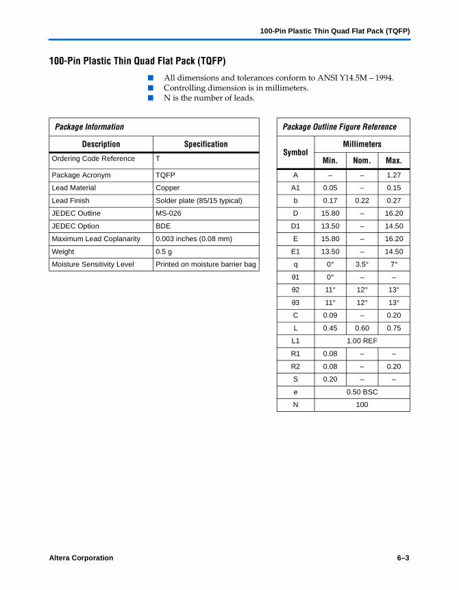
100-Pin Plastic Thin Quad Flat Pack (TQFP)
100-Pin Plastic Thin Quad Flat Pack (TQFP)
All dimensions and tolerances conform to ANSI Y14.5M – 1994. Controlling dimension is in millimeters. N is the number of leads.
Package Information Package Outline Figure Reference
Description SpecificationSymbol
Millimeters
Ordering Code Reference T Min. Nom. Max.
Package Acronym TQFP A – – 1.27
Lead Material Copper A1 0.05 – 0.15
Lead Finish Solder plate (85/15 typical) b 0.17 0.22 0.27
JEDEC Outline MS-026 D 15.80 – 16.20
JEDEC Option BDE D1 13.50 – 14.50
Maximum Lead Coplanarity 0.003 inches (0.08 mm) E 15.80 – 16.20
Weight 0.5 g E1 13.50 – 14.50
Moisture Sensitivity Level Printed on moisture barrier bag q 0° 3.5° 7°
θ1 0° – –
θ2 11° 12° 13°
θ3 11° 12° 13°
C 0.09 – 0.20
L 0.45 0.60 0.75
L1 1.00 REF
R1 0.08 – –
R2 0.08 – 0.20
S 0.20 – –
e 0.50 BSC
N 100
Altera Corporation 6–3Preliminary
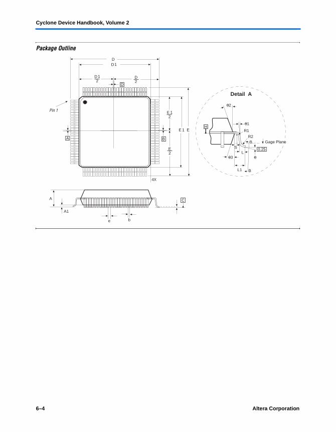
Cyclone Device Handbook, Volume 2
Package Outline
DD1
D1 D22
D
EE 1
E 1
E2
2
BA
4X
CA
e b
A1
Detail A
01
L
02
+R1
S
R2Gage Plane
L1
H
0.25
003
B
B
Pin 1
6–4 Altera CorporationPreliminary

144-Pin Plastic Thin Quad Flat Pack (TQFP)
144-Pin Plastic Thin Quad Flat Pack (TQFP)
All dimensions and tolerances conform to ANSI Y14.5M – 1994. Controlling dimension is in millimeters. N is the number of leads.
Package Information Package Outline Figure Reference
Description SpecificationSymbol
Millimeters
Ordering Code Reference T Min. Nom. Max.
Package Acronym TQFP A – – 1.60
Lead Material Copper A1 0.05 – 0.15
Lead Finish Solder plate (85/15 typical) b 0.17 0.22 0.27
JEDEC Outline MS-026 D 22.00 BSC
JEDEC Option BFB D1 20.00 BSC
Maximum Lead Coplanarity 0.003 inches (0.08 mm) e 0.50 BSC
Weight 1.3 g E 22.00 BSC
Moisture Sensitivity Level Printed on moisture barrier bag E1 20.00 BSC
q 0° 3.5° 7°
θ1 0° – –
θ2 11° 12° 13°
θ3 11° 12° 13°
L 0.45 0.60 0.75
L1 1.00 REF
R1 0.08 – –
R2 0.08 – 0.20
S 0.20 – –
N 144
Altera Corporation 6–5Preliminary

Cyclone Device Handbook, Volume 2
Package Outline
Pin 1
DD1
D1 D22
D
EE 1
E 1
E2
2
BA
A
A1
C
Detail A
01
L
02
+R1
S
R2Gage Plane
L1
H
0.25003
B
B
e
(n-4) X b
6–6 Altera CorporationPreliminary

240-Pin Plastic Quad Flat Pack (PQFP)
240-Pin Plastic Quad Flat Pack (PQFP)
All dimensions and tolerances conform to ANSI Y14.5M – 1994. Controlling dimension is in millimeters. N is the number of leads.
Package Information Package Outline Figure Reference
Description SpecificationSymbol
Millimeters
Ordering Code Reference Q Min. Nom. Max.
Package Acronym PQFP A – – 4.10
Lead Material Copper A1 0.25 – 0.50
Lead Finish Solder plate (85/15 typical) A2 3.20 3.40 3.60
JEDEC Outline MS-029 D 34.35 – 34.85
JEDEC Option GA D1 31.90 – 32.10
Maximum Lead Coplanarity 0.003 inches (0.08 mm) E 34.35 – 34.85
Weight 7.0 g E1 31.90 – 32.10
Moisture Sensitivity Level Printed on moisture barrier bag e 0.50 BSC
b 0.17 – 0.27
R2 0.08 – 0.25
R1 0.08 – –
q 0° 3.5° 8°
θ1 0° – –
θ2 5° – 16°
θ3 5° – 16°
L 0.46 – 0.66
L1 0.40 – –
S 0.20 – –
N 240
Altera Corporation 6–7Preliminary
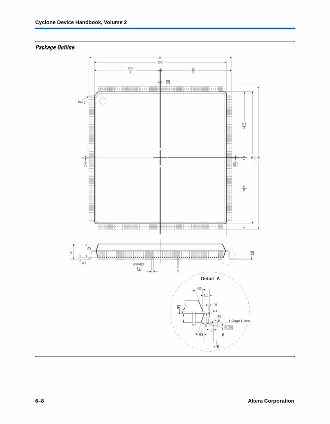
Cyclone Device Handbook, Volume 2
Package Outline
Pin 1
EE 1
E 1
E2
2
B
DD1
D1 D22
D
CAA2
A1
A
Detail A
01
L
02
+R1
L1
S
R2Gage Plane
H
0.25
003
B
B
b
(NÐ4)Xe
6–8 Altera CorporationPreliminary

256-Pin Non-Thermally Enhanced FineLine Ball-Grid Array
256-Pin Non-Thermally Enhanced FineLine Ball-Grid Array
All dimensions and tolerances conform to ANSI Y14.5M – 1994. Controlling dimension is in millimeters. M is the maximum solder ball matrix size.
Package Information Package Outline Figure Reference
Description SpecificationSymbol
Millimeters
Ordering Code Reference F Min. Nom. Max.
Package Acronym FBGA A (3) – – 3.50
Lead Material Tin-lead alloy (63/37) A1 0.30 – –
Lead Finish N/A A2 0.25 – 1.10
JEDEC Outline MS-034 A3 – – 2.50
JEDEC Option AAF-1 D/E 17.00 BSC
Maximum Lead Coplanarity 0.008 inches (0.20 mm) b 0.50 0.60 0.70
Weight 1.2 g e 1.00 BSC
Moisture Sensitivity Level Printed on moisture barrier bag M 16
(3) Altera’s thickness specification for A is 2.6 mm maximum. The Max item for A in the table reflects the JEDEC specification.
Altera Corporation 6–9Preliminary

Cyclone Device Handbook, Volume 2
Package Outline
Indicateslocation ofPin A1
Pin A1
G
F
E
D
C
B
A
H
J
K
L
M
N
P
R
T
16 15 14 13 12 11 10 9 8 7 6 5 4 3 2 1
A1A2
A
CSeating Plane
b
e
E
BDA
6–10 Altera CorporationPreliminary

324-Pin Non-Thermally Enhanced FineLine Ball-Grid Array
324-Pin Non-Thermally Enhanced FineLine Ball-Grid Array
All dimensions and tolerances conform to ANSI Y14.5M – 1994. Controlling dimension is in millimeters. M is the maximum solder ball matrix size.
Package Information Package Outline Figure Reference
Description SpecificationSymbol
Millimeters
Ordering Code Reference F Min. Nom. Max.
Package Acronym FBGA A (4) 1.20 – 3.50
Lead Material Tin-lead alloy (63/37) A1 0.30 – –
Lead Finish N/A A2 0.25 – 3.00
JEDEC Outline MS-034 D/E 19.00 BSC
JEDEC Option AAG-1 b 0.50 0.60 0.70
Maximum Lead Coplanarity 0.008 inches (0.20 mm) e 1.00 BSC
Weight 1.5 g M 18
Moisture Sensitivity Level Printed on moisture barrier bag (4) Altera’s thickness specification for A is 2.6 mm maximum. The Max item for A in the table reflects the JEDEC specification.
Altera Corporation 6–11Preliminary

Cyclone Device Handbook, Volume 2
Package Outline
Indicates Locationof Ball A1
123456789101112131415161718
ABCDEFGHJKLMNPRTUV
A1 Ball Pad Corner
AA1 CSeating Plane
E
BDA
b
e
A2
6–12 Altera CorporationPreliminary

400-Pin Non-Thermally Enhanced FineLine Ball-Grid Array
400-Pin Non-Thermally Enhanced FineLine Ball-Grid Array
All dimensions and tolerances conform to ANSI Y14.5M – 1994. Controlling dimension is in millimeters. M is the maximum solder ball matrix size.
Package Information Package Outline Figure Reference
Description SpecificationSymbol
Millimeters
Ordering Code Reference F Min. Nom. Max.
Package Acronym FBGA A (5) 120 – 3.50
Lead Material Tin-lead alloy (63/37) A1 0.30 – –
Lead Finish N/A A2 0.25 – 3.00
JEDEC Outline MS-034 D/E 21.00 BSC
JEDEC Option AAJ-1 b (6) 0.50 0.60 0.70
Maximum Lead Coplanarity 0.008 inches (0.20 mm) e 1.00 BSC
Weight 1.9 g M 18
Moisture Sensitivity Level Printed on moisture barrier bag (5) Altera's thickness specification for ‘A’ is 2.6 mm maximum. The Max. dimension for ‘A’ in the table reflects the JEDEC specification.
(6) Ball size, parameter ‘b’, can increase to a maximum of 0.74. Contact Altera Applications for more information.
Altera Corporation 6–13Preliminary

Cyclone Device Handbook, Volume 2
Package Outline
Indicates Locationof Ball A1
E
BDA
123456789101112131415161718
ABCDEFGHJKLMNPRTUV W Y
A1 Ball Pad Corner
e
b
1920
A
A1
A2
6–14 Altera CorporationPreliminary

Altera Corporation May 2003
C52007-1.0
7. Designing with FineLineBGA Packages
Introduction As programmable logic devices (PLDs) increase in density and I/O pins, the demand for small packages and diverse packaging options continues to grow. Ball-grid array (BGA) packages are an ideal solution because the I/O connections are on the interior of the device, improving the ratio between pin count and board area. Typical BGA packages contain up to twice as many connections as quad flat pack (QFP) packages for the same area. Further, BGA solder balls are considerably stronger than QFP leads, resulting in robust packages that can tolerate rough handling.
Altera has developed a new BGA solution for users of high-density PLDs called the FineLine BGAR package. The new format requires less than half the board space of standard BGA packages. This application note provides guidelines for designing your printed circuit board (PCB) for Altera’s FineLine BGA packages and discusses the following topics:
Overview of BGA packages PCB layout terminology PCB layout for FineLine BGA packages
Overview of BGA Packages
As PLDs grow to 1 million gates and beyond, designers require more advanced, flexible packages. BGA packages empower designers by offering the technological benefits and flexibility to meet future system requirements.
In BGA packages, the I/O connections are located on the interior of the device. Leads normally placed along the periphery of the package are replaced with solder balls arranged in a matrix across the bottom of the substrate. The final device is soldered directly to the PCB using assembly processes virtually identical to the standard surface mount technology preferred by system designers.
In addition, BGA packages provide the following advantages:
Fewer damaged leads—BGA leads consist of solid solder balls, which are less likely to suffer damage during handling.
More leads per unit area—Lead counts are increased by moving the solder balls closer to the edges of the package and by decreasing the pitch to 1.0 mm.
7–1Preliminary
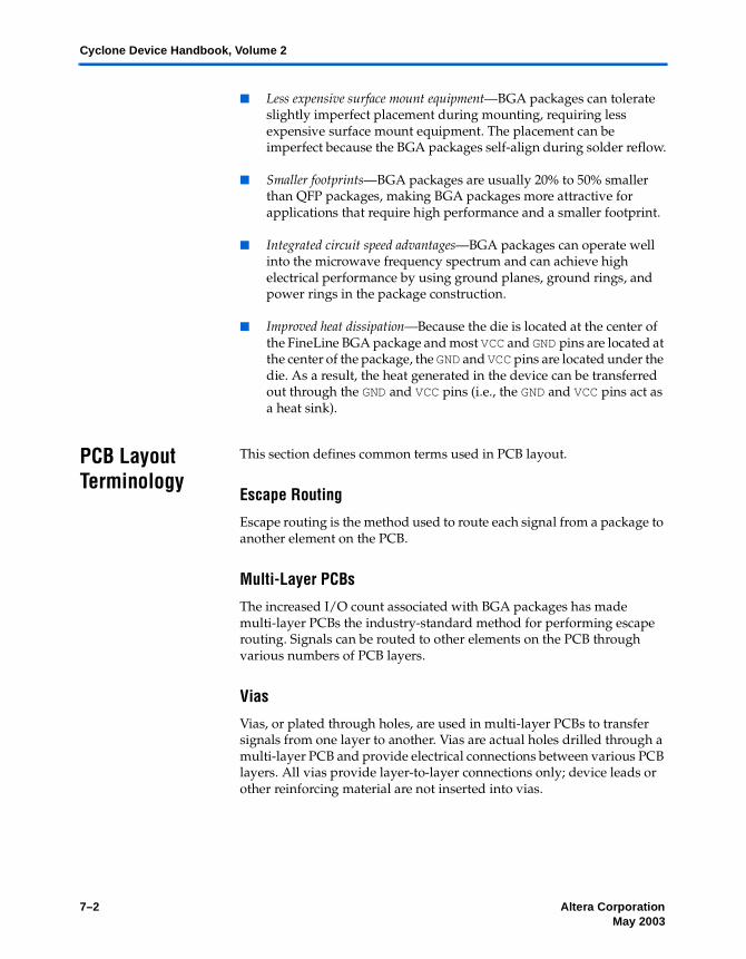
Cyclone Device Handbook, Volume 2
Less expensive surface mount equipment—BGA packages can tolerate slightly imperfect placement during mounting, requiring less expensive surface mount equipment. The placement can be imperfect because the BGA packages self-align during solder reflow.
Smaller footprints—BGA packages are usually 20% to 50% smaller than QFP packages, making BGA packages more attractive for applications that require high performance and a smaller footprint.
Integrated circuit speed advantages—BGA packages can operate well into the microwave frequency spectrum and can achieve high electrical performance by using ground planes, ground rings, and power rings in the package construction.
Improved heat dissipation—Because the die is located at the center of the FineLine BGA package and most VCC and GND pins are located at the center of the package, the GND and VCC pins are located under the die. As a result, the heat generated in the device can be transferred out through the GND and VCC pins (i.e., the GND and VCC pins act as a heat sink).
PCB Layout Terminology
This section defines common terms used in PCB layout.
Escape Routing
Escape routing is the method used to route each signal from a package to another element on the PCB.
Multi-Layer PCBs
The increased I/O count associated with BGA packages has made multi-layer PCBs the industry-standard method for performing escape routing. Signals can be routed to other elements on the PCB through various numbers of PCB layers.
Vias
Vias, or plated through holes, are used in multi-layer PCBs to transfer signals from one layer to another. Vias are actual holes drilled through a multi-layer PCB and provide electrical connections between various PCB layers. All vias provide layer-to-layer connections only; device leads or other reinforcing material are not inserted into vias.
7–2 Altera CorporationPreliminary May 2003
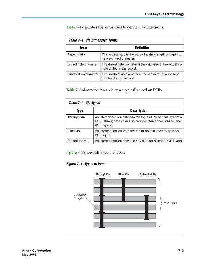
PCB Layout Terminology
Table 7–1 describes the terms used to define via dimensions.
Table 7–2 shows the three via types typically used on PCBs.
Figure 7–1 shows all three via types.
Figure 7–1. Types of Vias
Table 7–1. Via Dimension Terms
Term Definition
Aspect ratio The aspect ratio is the ratio of a via’s length or depth to its pre-plated diameter.
Drilled hole diameter The drilled hole diameter is the diameter of the actual via hole drilled in the board.
Finished via diameter The finished via diameter is the diameter of a via hole that has been finished.
Table 7–2. Via Types
Type Description
Through via An interconnection between the top and the bottom layer of a PCB. Through vias can also provide interconnections to inner PCB layers.
Blind via An interconnection from the top or bottom layer to an inner PCB layer.
Embedded via An interconnection between any number of inner PCB layers.
Connection to Layer
Through Via Blind Via Embedded Via
PCB Layers
Altera Corporation 7–3May 2003 Preliminary

Cyclone Device Handbook, Volume 2
Blind vias and through vias are used more frequently than embedded vias. Blind vias can be more expensive than through vias, but overall costs can be reduced because signal traces can be routed under a blind via, requiring fewer PCB layers. Through vias, on the other hand, do not permit signals to be routed through lower layers, which can increase the required number of PCB layers and overall costs.
Via Capture Pad
Vias are connected electrically to PCB layers through via capture pads, which surround each via.
Surface Land Pad
Surface land pads are the areas on the PCB to which the BGA solder balls adhere. The size of these pads affects the space available for vias and escape routing. In general, surface land pads are available in the following two basic designs:
Non solder mask defined (NSMD), also known as copper defined Solder mask defined (SMD)
The main differences between the two surface land pad types are the size of the trace and space, the type of vias you can use, and the shape of the solder balls after solder reflow.
Non Solder Mask Defined Pad
In the non solder mask defined (NSMD) pad, the solder mask opening is larger than the copper pad. Thus, the surface land pad’s copper surface is completely exposed, providing greater area to which the BGA solder ball can adhere (see Figure 7–2). Altera recommends that you use a NSMD pad for most applications because it provides more flexibility, fewer stress points, and more line-routing space between pads.
Solder Mask Defined Pad
In the solder mask defined (SMD) pad, the solder mask overlaps the surface land pad’s copper surface (see Figure 7–2). This overlapping provides greater adhesion strength between the copper pad and the PCB’s epoxy/glass laminate, which can be important under extreme bending and during accelerated thermal cycling tests. However, the solder mask overlap shrinks the amount of copper surface available for the BGA solder ball.
7–4 Altera CorporationPreliminary May 2003
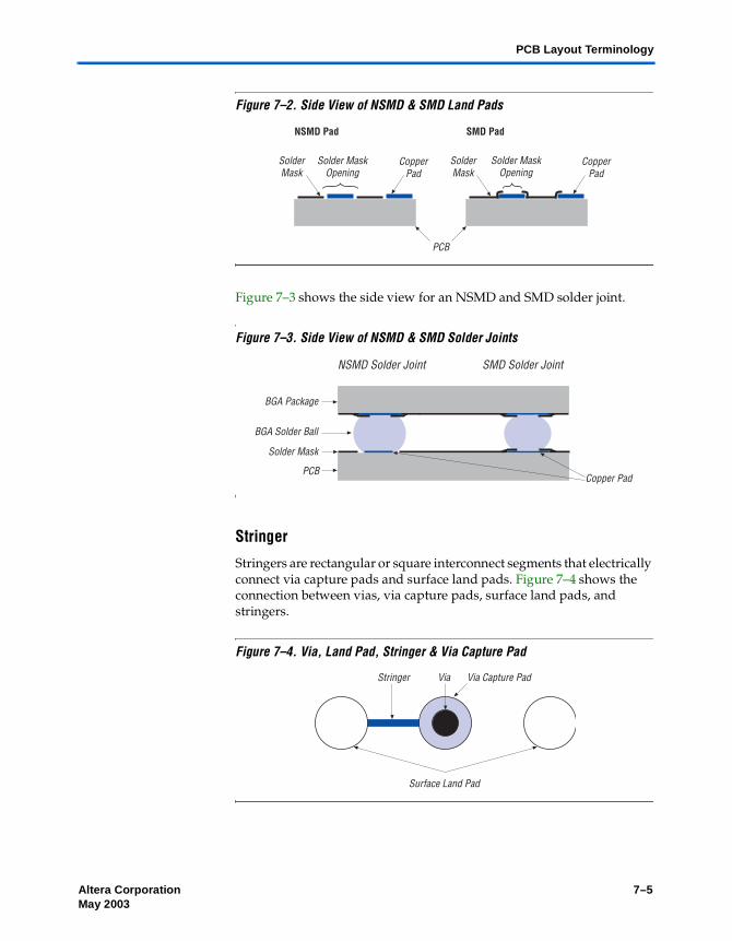
PCB Layout Terminology
Figure 7–2. Side View of NSMD & SMD Land Pads
Figure 7–3 shows the side view for an NSMD and SMD solder joint.
Figure 7–3. Side View of NSMD & SMD Solder Joints
Stringer
Stringers are rectangular or square interconnect segments that electrically connect via capture pads and surface land pads. Figure 7–4 shows the connection between vias, via capture pads, surface land pads, and stringers.
Figure 7–4. Via, Land Pad, Stringer & Via Capture Pad
PCB
Solder MaskOpening
Solder MaskOpening
SolderMask
CopperPad
SMD PadNSMD Pad
SolderMask
CopperPad
SMD Solder JointNSMD Solder Joint
BGA Solder Ball
Copper Pad
Solder Mask
PCB
BGA Package
Surface Land Pad
Stringer Via Capture PadVia
Altera Corporation 7–5May 2003 Preliminary

Cyclone Device Handbook, Volume 2
PCB Layout for FineLine BGA Packages
When designing a PCB for FineLine BGA packages, consider the following factors:
Surface land pad dimension Via capture pad layout and dimension Signal line space and trace width Number of PCB layers
1 For all FineLine BGA figures, the controlling dimension is millimeters.
Surface Land Pad Dimension
Surface land pads should be the same size as the BGA pad to provide a balanced stress on solder joints. For this reason, Altera recommends using a 15.75-mil surface land pad, because it is the same size as the BGA pad. Figure 7–5 shows a 15.75-mil BGA pad.
Figure 7–5. 15.75-Mil BGA Pad
Figure 7–6 shows how much space is available for vias and escape routing when you use 15.75-mil surface land pads.
(15.75 mil)0.40 mm
(25.00 mil)0.63 mm
BGA Pad
BGA Package
BGA Solder Ball
7–6 Altera CorporationPreliminary May 2003

PCB Layout for FineLine BGA Packages
Figure 7–6. Space Available for 15.75-Mil Surface Land Pads
Via Capture Pad Layout & Dimension
The size and layout of via capture pads affect the amount of space available for escape routing. In general, you can layout via capture pads in the following two ways: in-line with the surface land pads or in the diagonal of surface land pads. Figure 7–7 shows both layouts.
0.60 mm(23.62 mil)
0.60 mm(23.62 mil)
0.40 mm(15.75 mil)
Surface Land Pads
1.00 mm(39.37 mil)
1.01 mm(39.76 mil)
1.00 mm(39.37 mil)
Altera Corporation 7–7May 2003 Preliminary

Cyclone Device Handbook, Volume 2
Figure 7–7. Placement of Via Capture Pad
The decision to place the via capture pads diagonally or in-line with the surface lands pads is based on the following factors:
Diameter of the via capture pad Stringer length Clearance between via capture pad and surface land pad
To decide how to lay out your PCB, use the information shown in Figure 7–7 and Table 7–3. If your PCB design guidelines do not conform to either equation in Table 7–3, contact Altera Applications for further assistance.
Table 7–3 shows that you can place a larger via capture pad diagonally than in-line with the surface land pads.
Surface land pad
Via capture pad
Vias
Stringer
Stringer length a
Stringer widthb
Minimum clearance between via capture pad and surface land pad
c
Via capture pad diameterdTrace widthe
Space widthfArea for escape routing(This area is on a different PCB layer than the surface land pads.)
g
Diagonally
0.40 mm(15.75 mil)
a
c
1.00 mm(39.37 mil)
d
b
f
e
f
g
In Line
0.60 mm(23.62 mil)
0.40 mm(15.75 mil)
1.00 mm(39.37 mil)
a c
d
b
f
e
f
g
1.00 mm(39.37 mil)
Table 7–3. Formula for Via Layouts
Layout Formula
In-line a + c + d ð 23.62 mil
Diagonally a + c + d ð 39.76 mil
7–8 Altera CorporationPreliminary May 2003

PCB Layout for FineLine BGA Packages
Via capture pad size also affects how many traces can be routed on a PCB. Figure 7–8 shows sample layouts of typical and premium via capture pads. The typical layout shows a via capture pad size of 27 mil, a via size of 8 mil, and an inner space/trace of 4 mil. With this layout, only one trace can be routed between the vias. If more traces are required, you must reduce the via capture pad size or the space/trace size.
The premium layout shows a via capture pad size of 20 mil, a via size of 5 mil, and an inner space/trace of 3 mil. This layout provides enough space to route two traces between the vias.
Figure 7–8. Typical & Premium Via Capture Pad Sizes
Table 7–4 shows the typical and premium layout specifications used by most PCB vendors.
f For detailed information on drill sizes, via sizes, space/trace sizes, or via capture pad sizes, contact your PCB vendor directly.
Table 7–4. Vendor Specifications
Specification Typical (Mil) Premium (Mil)
Trace/space width 5/5 3/3
Drilled hole diameter 12 10
Finished via diameter 8 ð 5
Via capture pad 25.5 20
Aspect ratio 7:1 10:1
8.00 mil
27.00 mil
4 mil
39.37 mil
5.00 mil
20.00 mil
3 mil
39.37 mil
Typical Premium
Via
Via Capture Pad
Space
Trace
15.00 mil
Altera Corporation 7–9May 2003 Preliminary

Cyclone Device Handbook, Volume 2
Signal Line Space & Trace Width
The ability to perform escape routing is defined by the width of the trace and the minimum space required between traces. The minimum area for signal routing is the smallest area that the signal must be routed through (i.e., the distance between two vias, or g in Figure 7–7). This area is calculated by the following formula:
g = 39.37 – d
The number of traces that can be routed through this area is based on the permitted line trace and space widths. You can use Table 7–5 to determine the total number of traces that can be routed through g.
Figure 7–9 shows that by reducing the trace and space size, you can route more traces through g. Increasing the number of traces reduces the required number of PCB layers and decreases the overall cost.
Figure 7–9. Escape Routing for Double & Single Traces
Table 7–5. Number of Traces
Number of Traces Formula
1 g ≥ [2 × (space width)] + trace width
2 g ≥ [3 × (space width)] + [2 × (trace width)]
3 g ≥ [5 × (space width)] + [3 × (trace width)]
0.40 mm(15.75 mil)
0.60 mm(23.62 mil)
0.40 mm(15.75 mil)
0.12 mm(4.72 mil)
0.40 mm(15.75 mil)
0.60 mm(23.62 mil)
0.40 mm(15.75 mil)
0.20 mm(7.87 mil)
Double Trace Routing Single Trace Routing
Via Capture Pad
Space
Trace
7–10 Altera CorporationPreliminary May 2003

PCB Layout for FineLine BGA Packages
Number of PCB Layers
In general, the number of PCB layers required to route signals is inversely proportional to the number of traces between vias (i.e., the greater the number of traces, the fewer the number of PCB layers required). You can estimate the number of layers your PCB requires by first determining:
Trace and space size Number of traces routed between the via capture pads Type of vias used
Table 7–6 shows the number of PCB layers required to route signals for various FineLine BGA packages in EPF10K50E devices, assuming the use of a power plane, ground plane, and all I/O pins. This table shows that using double traces and blind vias reduces the required number of layers.
Using fewer I/O pins than the maximum can reduce the required number of layers. Via type can also reduce the number of layers required. To see how the via type can affect the required number of PCB layers, consider the sample layouts shown in Figure 7–10.
Table 7–6. Minimum Required PCB Layers
FineLine BGA Package (Balls)
Single Trace Double Trace
Blind Vias(Layers)
Through Vias(Layers)
Blind Vias(Layers)
Through Vias(Layers)
100 2 2 1 1
256 2 2 2 2
484 2 3 2 2
672 3 4 2 3
Altera Corporation 7–11May 2003 Preliminary
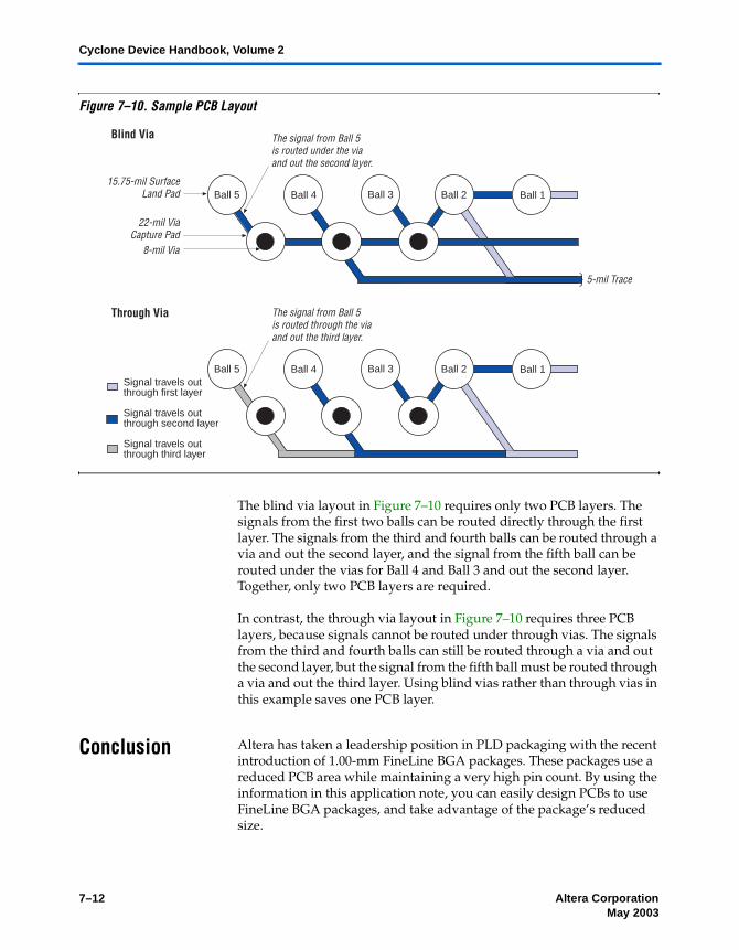
Cyclone Device Handbook, Volume 2
Figure 7–10. Sample PCB Layout
The blind via layout in Figure 7–10 requires only two PCB layers. The signals from the first two balls can be routed directly through the first layer. The signals from the third and fourth balls can be routed through a via and out the second layer, and the signal from the fifth ball can be routed under the vias for Ball 4 and Ball 3 and out the second layer. Together, only two PCB layers are required.
In contrast, the through via layout in Figure 7–10 requires three PCB layers, because signals cannot be routed under through vias. The signals from the third and fourth balls can still be routed through a via and out the second layer, but the signal from the fifth ball must be routed through a via and out the third layer. Using blind vias rather than through vias in this example saves one PCB layer.
Conclusion Altera has taken a leadership position in PLD packaging with the recent introduction of 1.00-mm FineLine BGA packages. These packages use a reduced PCB area while maintaining a very high pin count. By using the information in this application note, you can easily design PCBs to use FineLine BGA packages, and take advantage of the package’s reduced size.
Ball 1Ball 2Ball 3Ball 4Ball 5
Blind Via
8-mil Via
5-mil Trace
The signal from Ball 5is routed under the viaand out the second layer.
22-mil ViaCapture Pad
15.75-mil SurfaceLand Pad
Ball 1Ball 2Ball 3Ball 4Ball 5
Through Via The signal from Ball 5is routed through the viaand out the third layer.
Signal travels outthrough first layer
Signal travels outthrough second layer
Signal travels outthrough third layer
7–12 Altera CorporationPreliminary May 2003