-AI8I 470 THERMXONIC EMISSION MODEL FOR THE INITIAL … · -ai8i 470 a thermxonic emission model...
22
-AI8I 470 A THERMXONIC EMISSION MODEL FOR THE INITIAL REGIME OF / SILICON OXIDATION(IJ) NORTH CAROLINA UNIV AT CHAPEL HILL DEPT OF CHEMISTRY E A IRENE ET AL 8S JUN 87 TR-t4 UNCLASSIFIED N@8914-86-K-8285 F/G 712 MI. IEEE..',MMI
-
Upload
nguyenthien -
Category
Documents
-
view
214 -
download
0
Transcript of -AI8I 470 THERMXONIC EMISSION MODEL FOR THE INITIAL … · -ai8i 470 a thermxonic emission model...

-AI8I 470 A THERMXONIC EMISSION MODEL FOR THE INITIAL REGIME OF /SILICON OXIDATION(IJ) NORTH CAROLINA UNIV AT CHAPEL HILLDEPT OF CHEMISTRY E A IRENE ET AL 8S JUN 87 TR-t4
UNCLASSIFIED N@8914-86-K-8285 F/G 712 MI.
IEEE..',MMI
~~ ma
1.2 I-A -116
MICROCOPY RESOLUTION TEST CHART
NMIOW. BUREAU OF STANDARDS 1963-A

ITC FILE COY
O0
IOFFICE OF NAVAL RESEARCH
CONTRACT NO. N00014-86-K-0305
TECHNICAL REPORT NO. 14
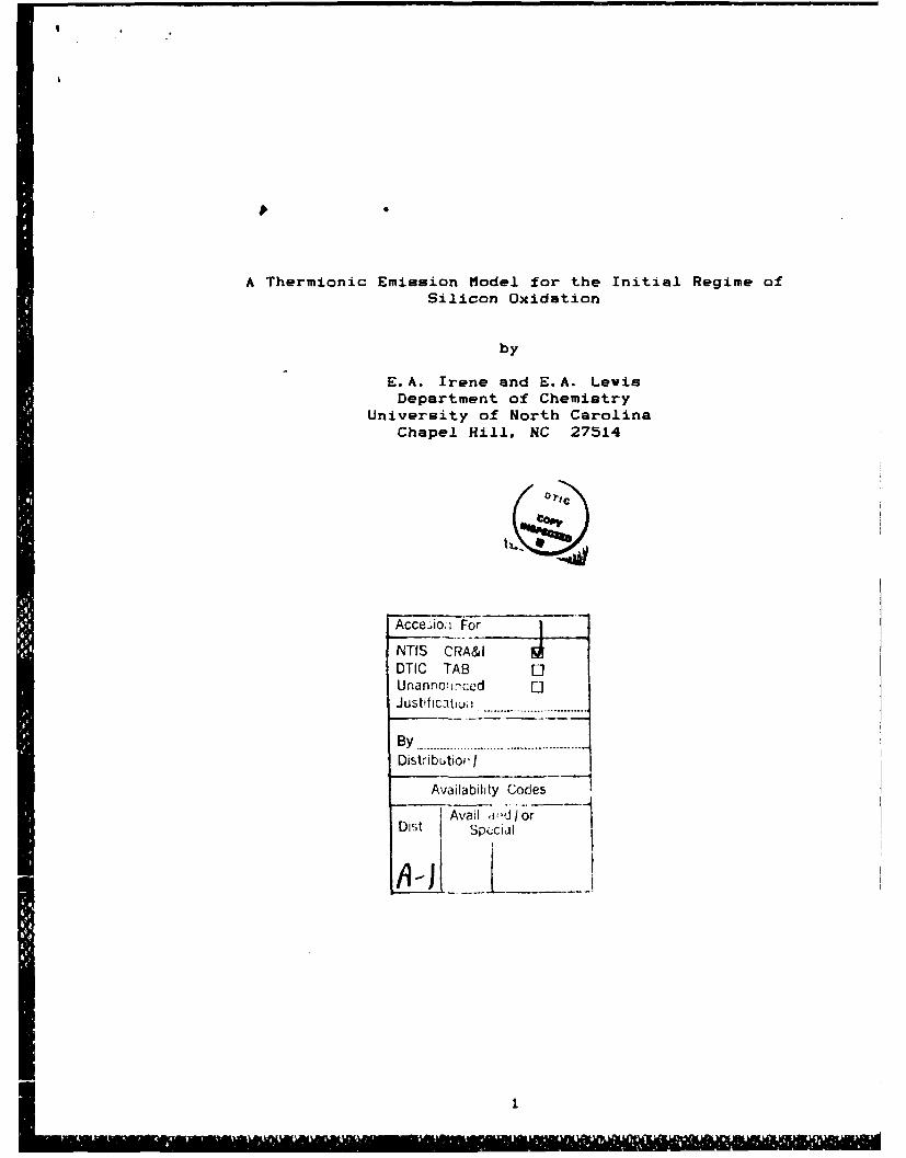
Thermionic Emission Model for the Initial Regime of Silicon Oxidation
E.A. Irene and E.A. Lewis D T ICDepartment of Chemistry
University of North Carolina ELECTEChapel Hill, NC 27514 S JUN 17 1987DJ
in ~, D
Applied Physical Letters
Reproduction in whole or in part is permitted for any purpose of the UnitedStates Government.
This document has been approved for public release and sale; its distributionis unlimited.
006

REPORT DOCUMENTATION PAGE
,. REPORT SECURITY CLASSIFICATION 1b. RESTRICTIVE MARKINGS
Unclassified2. SECURITY CLASSIFICATION AUTHORITY 3 OISTRIUTION,AVAILAOI ITY OF REPORT
2b. OECLAIFICATION/OOWNGRAOINGSCNEOULE Approved for public release; distributionunlimited.
4 PERFORMING ORGANIZATION REPORT NUMBERIS) S. MONITORING ORGANIZATION REPORT NUMSERIS)
Technical Report #14
G. NAME OF PERFORMING ORGANIZATION b. OFFICE SYMBOL 76. NAME OF MONITORING ORGANIZATION
UNC Chemistry Dept. Office of Naval Research (Code 413)
6c. ADDRESS (Ci y. State .nd ZIP Code) Tb. ADDRESS (City. Sc-e. and ZIP Codet
11-3 Venable Hall 045A Chemistry ProgramChapel Hill, NC 27514 800 N. Quincy Street
Arlington, Virginia 22217B. NAME OF FUNOING/SPONSORING 8b. OFFICE SYMBOL 9. PROCUREMENT INSTRUMENT IDENTIFICATION NUMBER
ORGANIZATION (if applicabe)Office of Naval Research Contract #N00014-86-K-0305
dc ADDRESS ICly. Stale and ZIP CodeI 10 SOURCE OF FUNDING NOS
Chemistry Program PROGRAM PROJECT TASK WORK UNITCeityPormE LE MENT NO NO NO. NO800 N. Quincy, Arlington, VA 22217
11. TITLE (Include Securety Cmeafication, A THKMInUNoC nI. .LMODEL FOR THE INITIAL REGIME OF SILICON OXIDA ON12. PERSONAL AUTmOR(S)
E.A. Irene and E.A. Lewis13&. TYPE OF REPORT 13b. TIME COVEREO 14. DATE OF REPORT (yr.. Mo.. Day) 15. PAGE COUNT
Interim Technical FROM - To June 3, 1987 161S. SUPPLEMENTARY NOTATION
Prepared for publication in Applied Physical Letters
17 COSATI CODES 1E. SUBJECT TERMS (ContInu on Feueroe if necearmy and identify by block number)
FIELO GROUP SUB GR
It. A CT ICon gu1u on .'erwe If oecess ry and adrhoety by block numberl
The very early stage of the thermal oxidation of single crystal Si has been thesubject of continual study for the last two decades. In the light of very recentexperimental oxidation data on the initial regime, we report that a simple thermionicelectron flux from gS into S0iO 2 closely agrees with the SiO 2 film growth rate. Theimportance of elec ons for tpe oxidation kinetics has also been attested to in severalrecent experimenta4 studies./ Thus a consistent model is presented for the initialoxidation regime iased on th electron flux as the rate limiting step.
200 ISTRI BUTION/AVAILASILITY OF ABSTRACT 21 ABSTRACT SECuRiTY CLASSIFiCATION
.NCLASIII/UNLIMITEO SAME AS RPT 9 OTIC USERS 0 Unclassified
22a NAME OP RESPONSIBLE INDIVIDUAL 22b TELEPHONE NUMBER 22c OFFICE SYMBOLfinelude A le CodeI
Dr. David L. Nelson (202) 696-4410
A Thermionic Emission Mlodel for the Initial Regime ofSilicon Oxidation
by
E.A. Irene and E.A. LevisDepartment of Chemistry
University of North CarolinaChapel Hill, NC 27514
r'j
Acce~i For
NTf S CRA&MOTIC TAB EUnannoi-mc d El
By .............. ...........Distributioni I
Availability Codes- i
D~ va d or 1Dis _L2Cd
Abstract
The very early stage of the thermal oxidation of singlecrystal Si has been the subject of continual study for the lasttwo decades. In the light of very recent experimental oxidationdata on the initial regime, we report that a simple thermionicelectron flux from Si into SiOC closely agrees with the SiO filmgrowth rate. The importance of electrons for the oxidationkinetics has also been attested to in several recent experimentalstudies. Thus a consistent model is presented for the initialoxidation regime based on the electron flux as the rate limitingstep.
The kinetics for the formation of SiOa films on Si has
received considerable attention both from the technological and
scientific viewpoint (see refs. 1-5 and refs. therein). Many
models have been proposed (see refs. 1,4,5 and references
therein) based on new phenomena incorporated into the Linear-
Parabolic, L-P, model proposed in the 1960's(6-8). This latter
model considers only the processes of transport of oxidant and
reaction of oxidant and silicon in a steady state and as
kinetically simple processes. However, a growing body of
studies(1,4,5 and references therein) now show that the simple L-
P model is inadequate and further elucidation of what was thought
to be simple processes is necessary. Of particular relevance are
a number of studies on the initial oxidation regime which have
implicated the interface reaction as the dominating process(9-17)
for SiOe films thinner than 100nm.
The purpose of this letter is to show that a key step in the
interface reaction process is the emission of electrons from Si
to SiO. This idea was suggested in a number of earlier
studies(14,17-20), but quantification has not been possible
because the appropriate experimental oxidation data has only
recently become available.
Calculations comparing the maximum diffusion flux of oxygen
with oxidant flux obtained from the experimental oxidation rates
have shown that transport is not rate limiting below at least
100nm(10,18-20). Random walk calculations and a consideration
of the thermodynamic potentials for transport and the interface

reaction further support that the interface reaction must be
considered in the Si oxidation process(18-20). A steady state
between these two processes likely occurs with the interface
reaction having the smaller maximum value. This steady state
situation is complex and treated in more detail elsewhere(20).
Recently, there has been substantial experimental evidence
supporting the kinetic importance of the interface reaction in
the initial regime of oxidation. The very recent extensive
oxidation data of Lewis et al.(10,12) using five Si orientations
is concordant with previous studies(9,13) that show the oxidation
rate order parallels the Si atom areal density for the initial
oxidation regime. Perhaps more significant is the new finding
the the rates of oxidation are orientation dependent even well
beyond 100nm SiOG growth(10).
Two recent studies have strongly suggested the importance of
the availability of electrons to the oxidation mechanism. The
study of photon enhanced oxidation by Young and Tiller(14) shows
that there are three regimes of photon energy that enhance the
oxidation rate. Photon energies above 3eV show large enhancements
of more than ten fold compared with lower energies. The 3eV and
higher energy photons likely excite electrons over the Si-SiO.
barrier. The 5eV and greater energy radiation decomposes 0. to
atomic oxygen with a resulting enhancement compared to the 3eV
energies. The recent work by d'Heurle et al. (15) and Frampton et
al. (16) shows that different metal silicides, that are oxidized
under conditions which preserve the silicide film and form only
4
S4O., display oxidation rates in the order dictated by the
availability of free electrons on the silicide surface. This
finding supports previous studies by Cros(17) which strongly
suggested that the higher density of electrons at the Fermi level
was influential in determining the Si oxidation rate.
The control of the oxidation kinetics at the Si-SiOa
interface, plus the requirement for electrons enables the
following formulation of a new Si oxidation model based on
thermionic emission of electrons from Si into SiOa. Thermionic
emission of electrons in terms of the electron flux, F.,, is
governed by the Richardson-Dushman equation which may be written
as:
F,, = ATaexp(-X,/kT) (2)
where A is the Richardson constant, T is absolute temperature,
and X. is the barrier height which for metals extends from the
Fermi energy to vacuum for thermionic emission to vacuum. For the
case of emission from Si to SiOa, we modify the situation by
considering electron emission from levels in Si that have
sufficient electrons for the oxidation reaction. From the band
diagram in Figure 1, several options are seen for the promotion
of an electron from Si to the SiOa conduction band. The emission
from the densely populated Si valence band requires about 4.25eV,
from the intrinsic Fermi level of Si about 3.70eV, and from the
Si conduction band about 3.15eV is required.
5

The model assumes that the electron flux into SiO& is rate
limiting and governed by the Richardson equation. We show first
that this choice for the rate limiting flux is reasonable, and
then the specific mechanism steps are presented. Depicted in
Figure 2 are the fluxes now considered. It was previously
shown(10,18-20) that the maximum diffusive flux of oxidant, F(D),
is larger than the experimental flux of O, F(exp). Before we
focus on the assumed rate limiting -ep, F.t, the electron flux
to the Si surface, F., must be considered. This flux can be
estimated from the relationships:
F, = DN,/L, (3)
D. u.(kT/e) (4)
where D. and N, are the electron diffusivity and concentration,
respectively, V, is the electron mobility, and L. is the distance
into the bulk Si away from the oxidized surface. Using
literature values for a. and N., it is found that even at L,
values greater than 10anm the electron flux is 106 times larger
than the oxidation rate. Thus, with the three flux situation in
Figure 2, only the electron flux over the barrier, F.,, remains
for evaluation.
In order to establish that F., is a possible rate limiting
flux, the values of X, that yield values for F., which are
identical to the experimental oxidation flux, F(exp) are
p6

calculated. The X. values required for the equivalency of F..
with F(exp) are shown in Table 1 for several oxidation
temperatures. Several points are made from this Table. First, and
most important, is the finding that at all temperatures the
calculated value for X. corresponding to the very initial SiO&
growth regime is within about 0.2eV of the barrier of 3. 15eV from
the bottom of the Si conduction band. While this result seems
impressive, it should be remembered that a value of 0.2eV alters
the electron flux, F.,, by about 101. The agreement could be
physically significant, however, considering that the position of
the SiO. band edge has at least tenths of an eV uncertainty at
room temperature, and at the higher temperatures is more
uncertain. Based on experiments on the AI-SiOa interface(22) in
which it is observed that the barrier is apparently lowered at
elevated temperatures, it is quite likely that the Si-SiOs
barrier is also lowered at higher temperatures. However, it is
also known that the Si band gap decreases at elevated
temperatures(21), thereby populating higher levels in the Si
conduction band. Thus the precise definition of the band edges is
uncertain to at least several tenths of an eV. Next is the result
that the (110) orientation, the fastest oxidizing Si surface in
the initial regime consistently displays the lowest X.. It is
clear that this difference is forced by the requirement of the
equivalence of the fluxes. An independent measurement of the
barrier on different orientations would provide confirmation for
the proposed model. There is the general result that for all
7
temperatures and orientations there is an apparent increase in X.
for the larger film thicknesses. This is most noticeable for the
higher oxidation temperatures where, due to experimental
difficulties, there is no reliable data available for SiOa less
than 5nm. This effect is also likely an artifact due to the
growing importance of other kinetically significant processes
such as transport of oxidant, film stress or the reduction of the
oxidant concentration at the interface.
The question whether there are sufficient electrons in the
Si conduction band to permit F., to control the rate is answered
affirmatively for any temperature above room temperature. At room
temperature there is near equivalence at about 1016cm- 2 for both
the number of electrons required considering one per 0, molecule
and actually present. Another question arises from the
observation that even at room temperature, a Inm native oxide
grows rapidly on the Si surface and then oxidation is slow up to
2nm where oxidation essentially stops unless impurities are
present or the temperature is raised. The question is how does
this oxide grow without sufficient electrons (or at least
marginally sufficient) and then why does it stop? This problem
is understood if we consider that a restricted number of
electrons are available in defect states on the Si surface, ie.
so called surface states. Such states are known to trap
electrons(23), and thus provide a limited source of electrons
other than by emission over the barrier (perhaps by a tunneling
mechanism for example). In order to form 1nm of SiOs per cmt
8

requires about 2 x 10¹³ electrons at one electron per SiOa
molecule. This number is approximately equal to the
experimentally determined number of surface states per cm2 on a
freshly cleaved Si surfaceC24). Thus an initial native oxide
about Inm thick would have sufficient electrons available to form
rapidly and without high temperatures, as is observed. It follows
that once the Inm SiOn forms, the surface states are reduced to
below the 1010 cm -8 level, the barrier is formed, and the
emission process over the barrier is rate limiting.
With the flux of electrons as the rate limiting step, the
oxidation mechanism is envisioned to have the following four main
steps with step two being rate limiting:
1. In the Si conduction band:
Si -+ Si* - e-
2. At the Si-SiOg barrier:
e- (Si C.B.) e-(SiOe C.B. )
3. In SiOa:
0, + e- 0- + 0
4. The interfacial reaction:
Si* + 0- + 0 -+ SiOt
Accordingly, both the formation and reaction of atomic 0 is
important in this mechanism. The electron attachment reaction to
O& is not only a favored thermodynamical process, but also the
resulting molecular ion, Os-, has a lower dissociation energy
thereby producing more atomic 0 species(25). The importance of
the reaction of atomic oxygen with Si has been discussed by Ghez
9
and van der Meulen(26) to explain the pressure dependence of the
oxidation rate, by Blanc(27) to explain the unusually fast
initial oxidation regime and by Irene(28) to explain the
curvature of Arrhenius plots of the initial regime rate constant.
With this thermionic model, several perplexing facts about
Si oxidation in the very initial oxidation regime become
obviated. The observed sensitivity of the oxidation kinetics to
impurities and indeed to the cleaning process for the Si
M wafers(29,30) is understood in the context of recent studies that
shows that changes in barrier heights of tenths of an eV are
measured for nickel silicides on silicon when interfacial defects
and common impurities such as C are present(31). The rapid
formation of an initial oxide of about inm on Si with the
subsequent decrease in rate to low values requiring high
temperatures for oxidation to proceed measurably is also
explained.
The authors gratefully acknowledge useful discussions with
W.A. Tiller and F.M. d'Heurle. This research was supported in
part by the Office of Naval Research (ONR).
10
lA
References
1. E.A. Lewis and E.A. Irene, J. Vac. Sci. Technol. A, 4, 916 (1986).
2. S. Rigo, "Instabilities in Silicon Devices: Silicon Passivation and Related
Instabilities," Eds. G. Barbotten and A. Vapaille, Elsevier (1986) Chapter 1, "Silica
Films on Silicon."
3. A. Atkinson, "Transport Processes during the Growth of Oxide Films at ElevatedTemperatures," Rev. Mod. Phys., 57, 439 (1985).
4. E.A. Irene, Semiconductor International, p. 99, April 1983, and p. 92, June 1985.
5. E.A. Irene, "Passivity of Metals and Semiconductors," Ed. Michel Froment, Elsevier(1983), p. 11.
6. B.E. Deal and A.S. Grove, J. Appl. Phys., 36, 3770 (1965).
7. W.A. Pliskin, IBM J. Res. Dev., 10, 198 (1966).
8. A.G. Revesz, K.H. Zaininger and R.J. Evans, Appl. Phys. Lett., 8, 57 (1966).
9. H.Z. Massoud, J.D. Plumer and E.A. Irene, J. Electrochem. Soc., 132, 745, 2685, 2693(1985).
10. E.A. Lewis and E.A. Irene, J. Electrochem. Soc., in press (1987).
11. W.A. Tiller, J. Electrochem. Soc., 127, 625 (1980).
12. E.A. Lewis, E. Kobeda and E.A. Irene, "Semiconductor Silicon 1986," Eds. H.R. Huff,
T. Abe and B. Kolbesen, p. 416.
13. E.A. Irene, H.Z. Massoud and E. Tierney, J. Electrochem. Soc., 133, 1253 (1986).
14. E.M. Young and W.A. Tiller, Appl. Phys. Lett., 42, 63 (1983); 50, 80 (1987).
15. F.M. d'Heurle, A. Cros, R.D. Frampton and E.A. Irene, Phil. Mag. B, 55, 291 (1987).
16. R.D. Frampton, E.A. Irene and F.M. d'Heurle, J. Appl. Phys., submitted for publication
1987.
17. A. Cros, J. Physique, 44, 707 (1983).
18. E.A. Irene, Phil. Mag. B, 55, 131 (1987).
19. E.A. Irene, presented at Oct. 1986 Electrochemical Soc. Meeting, Abs. 364.
20. E.A. Irene and R. Ghez, Applied Surface Science, in press (1987).
21. S.M. Sze, "Physics of Semiconductor Devices," Wiley, 1981.
22. M4. AvRon, M4. Shatzkes, T.H. Di Stefano and R.A. Gdula, J.Appl. Phys., 52, 2907 (1981).
23. E.H. Poindexter, P.J. Caplan, J.J. Finnegan, N.M. Johnson, D.K. Biegisen and M.D. Moyer,in "Physics of MOS Insulators," G. Lucovaky, S.T. Pantelides and F.L. Galeener, Eds.,Pergamon, N.Y., 1980, p. 326.
24. E.H. Nicollian and J.R. Brevs, in "1405 (Metal Oxide Semiconductor) Physics andTechnology," Wiley, 1982.
25. L.M. Chanin, A.V. Phelps and M.A. Biondi, Phys. Rev., 128, 219 (1962).
26. R. Ghez and Y.J. van der lMeulen, J. Electrochem. Soc., 119, 1100, (1972).
27. J. Blanc, Appl. Phys. Lett., 33, 424, (1978).
28. E.A. Irene, Appi. Phys. Lett., 40, 74 (1982).
29. F.N. Schwettman, K.L. Chiang and W.A. Brown, 153rd," Electrochemical Soc.
Meeting, Abs. 276, May 1978.
30. G. Gould and L.A. Irene, J. Electrochem. Soc., (1987).
31. M4. Liehr, P.E. Schmid, F.K. LeGoues and P.S. Ho, J. Vac. Sci. Technol. A,4, 855, (1986).
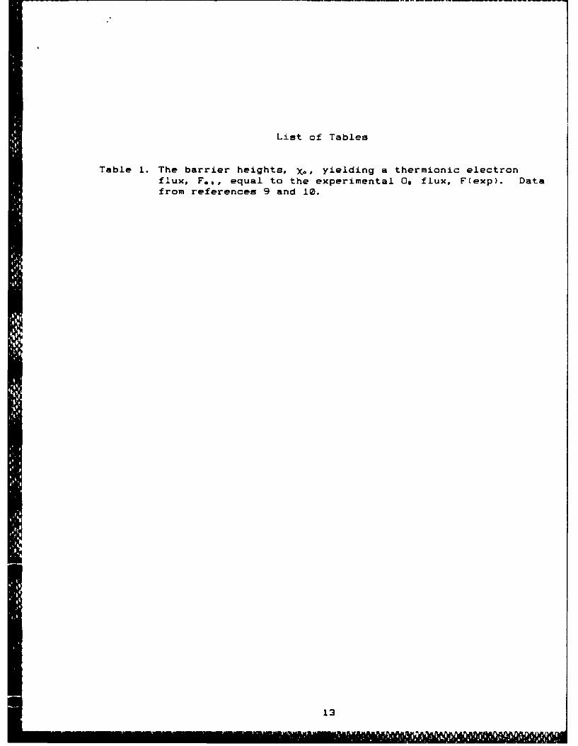
List of Tables
Table 1. The barrier heights, x., yielding a thermionic electronflux, F.,, equal to the experimental Oa flux, F(exp). Datafrom references 9 and 10.
13
List of Figures
Figure 1. Energy band diagram for Si-SiOa.
Figure 2. The fluxes for the thermionic emission model: F(D), thediffusive flux; F., the electron flux; and F,t, thethermionic emission flux of electrons.
14wunan"MfI

Table 1
Oxidation Si Oxidation Rate SiOa Thickness x0Temperature Orientation Range
(OC) (nm/min) (nm) (eV)
600 (100) 0.0004 2-3 2.87(110) 0.0012 2.5-6 2.79
650 (100) 0.014 2.5-7 2.95(110) 0.041 2.5-10 2.86
700 (100) 0.014 2.5 2.920.0057 10 3.000.0043 20 3.02
(110) 0.033 2.5 2.850.014 10 2.920.0094 20 2.96
750 (100) 0.028 5 3.020.024 10 3.030.019 20 3.06
(110) 0.057 5 2.960.035 10 3.000.024 20 3.04
1000 (100) 1.79 7 3.350.9 20 3.430.27 100 3.56
(110) 3.45 9 3.281.74 20 3.350.4 100 3.52
15
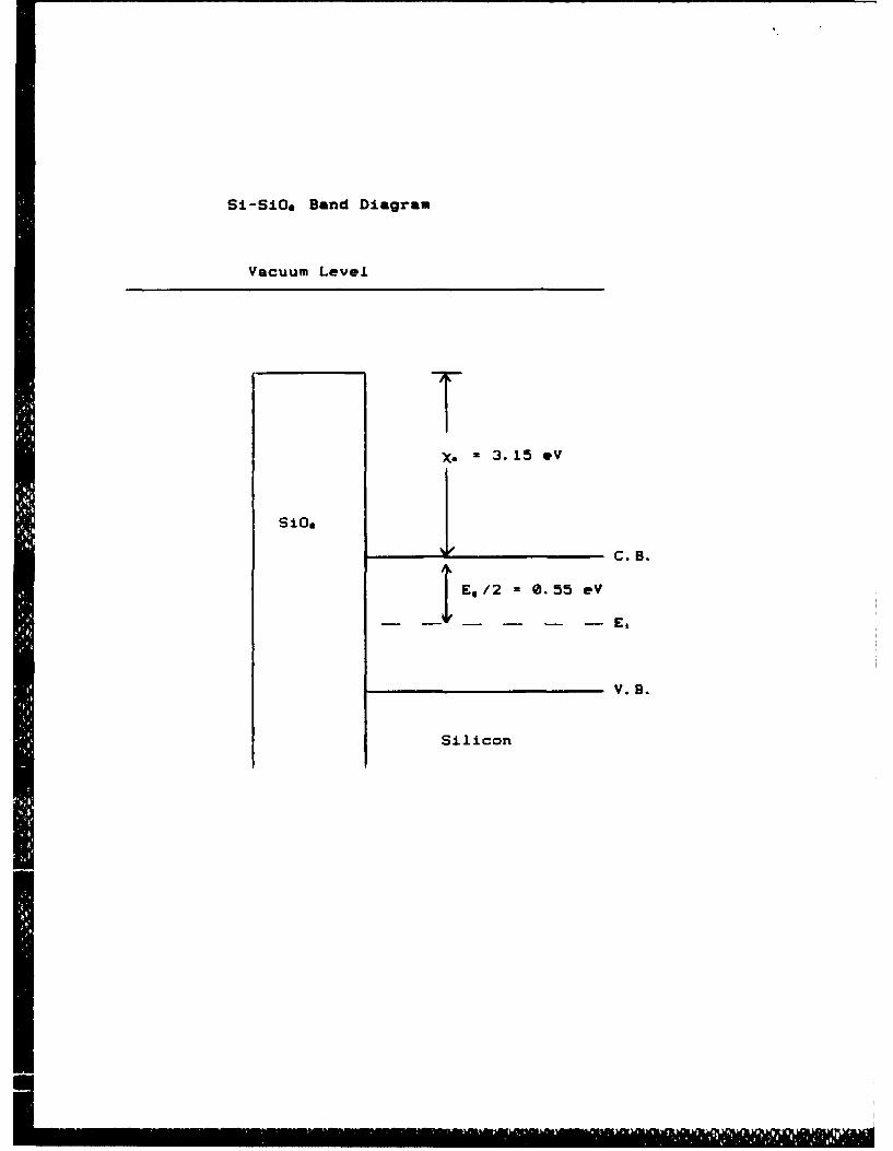
Si-SiG. Band Diagram
Vacuum Level
TX z 3. 15 eV
SiG. 1-C.B.IE,/2 =0.55 eV
Silicon
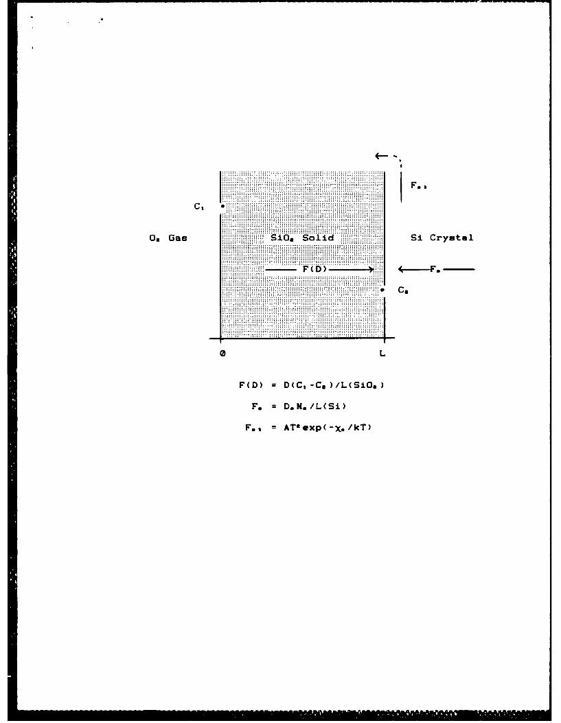
F..
C,
0. Gas Sid&'..Sol. Si Crystal
F(D) ~~ (DC-C)/(i)
F(. D(N./L(S)(is
F,.. ATexp(-X(./kT)