
-::2CL~ ' /IIIIVEUTEC - QSL.net 2 BASIC OPERATING PROCEDURES 2.1 GENERAL INFORMATION The SP-605H and...
20
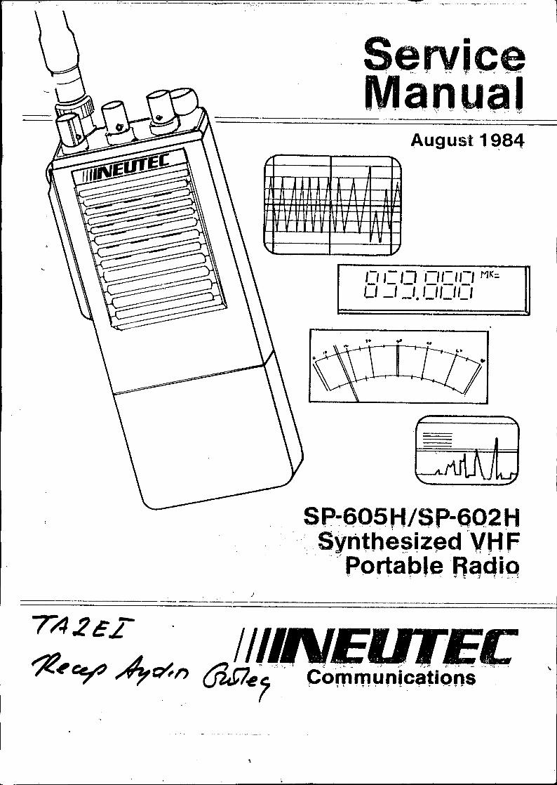
------- ---.-- '1::. -'"'7_~"~---'---.--~_.'-----~~-~-~"-------- -........-- ---~~ , ..... Service Manual August 1~84 ,-, ,- ,-" 11-"-' MK= Cİ _i _'. '_'CJ'-, SP-(j05H/SP-ft02H ...Syntheşiz~d VtiF " 'fPortatı'e R~~~p / -::2CL~_' /IIIIVEUTEC '/<.'0/ ".,-?cr;n @£joe, ..- Conımurıications
Transcript of -::2CL~ ' /IIIIVEUTEC - QSL.net 2 BASIC OPERATING PROCEDURES 2.1 GENERAL INFORMATION The SP-605H and...
------- ---.-- '1::. -'"'7_~"~---'---.--~_.'-----~~-~-~"---------........-----~~,.....
ServiceManual
August 1~84
,-, ,- ,-" 11-"-' MK=
Cİ _i _'. '_'CJ'-,
SP-(j05H/SP-ft02H. ..Syntheşiz~d VtiF
" 'fPortatı'e R~~~p/
-::2CL~_' /IIIIVEUTEC'/<.'0/ ".,-?cr;n @£joe, ..- Conımurıications
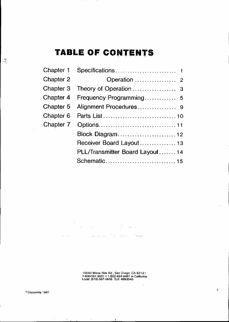
TABLE OF CONTENTS. - ,- ,,:
Chapter 1Chapter 2Chapter 3Chapter 4Chapter 5Chapter 6Chapter 7
"Copywril~ 1987
Specifications .... __ _. . . . . . . . . . . . . .. 1
Operation 2
Theory of Operation. . . . . . . . . . . . . . . . .. 3
Frequency Programming. . . . . . . . . . . .. 5
Alignment Procedures. . . . . . . . . . . . . . .. 9
Parts List 1 O
Options 11
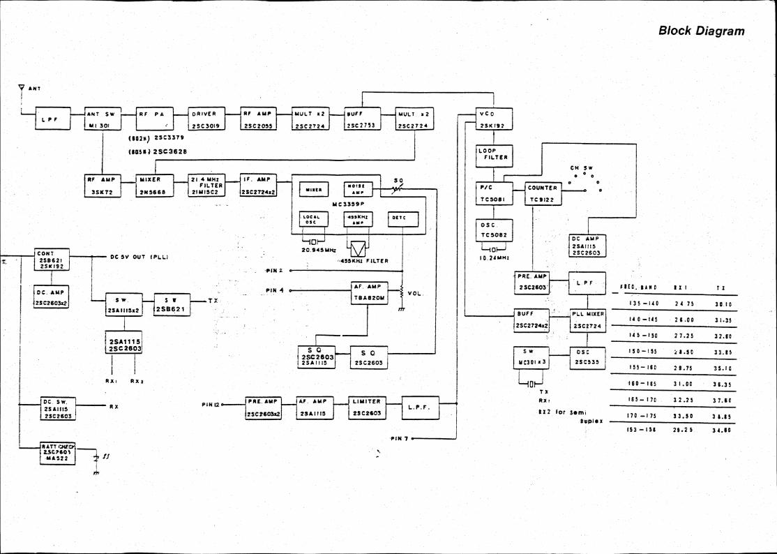
Block Diagram .- 12
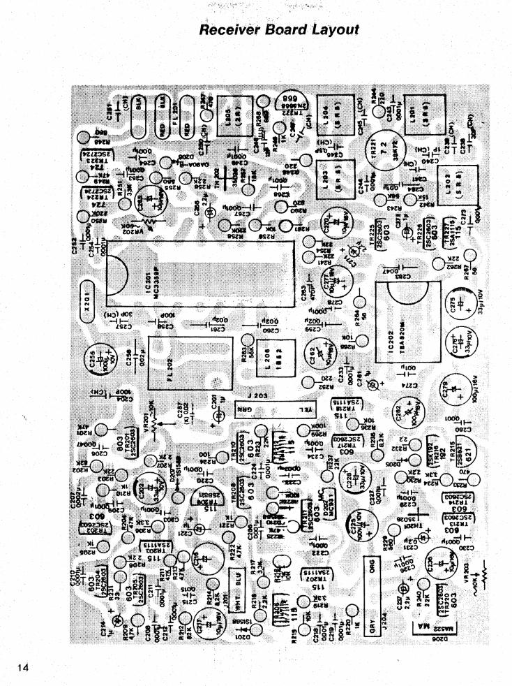
Receiver Board Layout. 13
PLLITransmitter Board Layout 14
Schematic 15
10040 Mesa Aim Ad., San Diego, CA 921211-800-551 8551 • 1-800-424-8491 in CaliforniaLocal: (619) 587-0656 TLX: 4993540
CHAPTER 1" ,'~ -'I ., -~ ,J ,
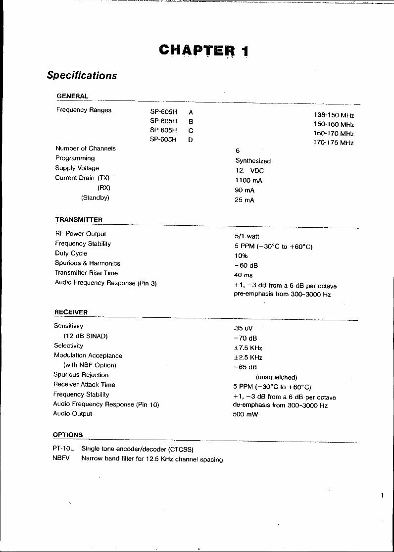
Specifica tions
GENERAL
Frequency Ranges
Number of ChannelsProgramming
Supply VoltageCurrent Drain (TX)
(RX)
(Standby)
TRANSMITTER
SP-605H ASP-605H BSP-605H CSP-605H D
138-150 MHz150-160 MHz160-170 MHz170-175 MHz
6
Synthesized12. VDC1100 mA90 mA25 mA
RF Power OutputFrequency StabilityDuty Cycle
Spurious & HarmonicsTransmitter Rise Time
Audio Frequency Response (Pin 3)
RECEIVER
Sensitivity
(12 dB SINAD)SelectivityModulation Acceptance
(with NBF Option)Spurious RejectionReceiver Attack Time
Frequency StabilityAudio Frequency Response (Pin 10)Audio Output
OPTIONS
PT-1OL Single tone encoder/decoder (CTCSS)NBFV Narrow band filter for 12.5 KHz channel spacing
5/1 watt
5 PPM (-30°C to +60°C)10%-60 dB40 ms
+ 1, -3 dB from a 6 dB per octavepre-emphasis from 300-3000 Hz
.35 uV-70 dB:t7.5 KHz:t2.5 KHz-65 dB
(unsquelched)5 PPM (,-30°C to +60°C)
+ 1, -3 dB from a 6 dB per octavede-emphasis from 300-3000 Hz500 mW
1

CHAPTER 2BASIC OPERATING PROCEDURES
2.1 GENERAL INFORMATION
The SP-605H and SP-602H portable transeeiyers are the firstall metal, synthesized, low-eost handhelds speeifieallydesigned for the professional land mobile user. These unitsoperate in the VHF/FM band from 136 MHz to 174 MHz. Thespeeifie frequency of operation is determined by the diode-matrix board and the eorresponding ranging erystal. Byeliminating the need of frequency crystals for each channel,future ehannel additions are easily accommodated and thedelay time of waiting for erystals is eliminated.
Power output for the SP-605H is fiye watts in the HI positionand one watt in the LO position. The SP-602H proYides twowatts of RF output in the HI position and 0.5 watts in the LOsetting. By utilizing the LO power position wheneyer pos-sible, the battery consumption is reduced to allow longer usebetween battery charges.
Battery power for the SP-605H is proYided by a slip-on 12.0yolt pack. The SP-602H uses a smaIler pack of the same stylewith a voltage of 7.2 volts. Both of these battery paeks areeasily changed by the user. For optimum performance, theseniekel cadmium paeks should be completely disehargedperiodieally prior to recharges. This allows the battery totake on a deeper charge whieh offers a longer use beforeminimum operating voltage is reaehed.
~ ~ OPERATING PROCEDURES
2.21 ANTENNAThe helical whip (50 ohm) antenna is secured to the portableat the BNC connector. To install the antenna the eonneetorsshould be mated and th~ connector turned elockwise untillocked.
2.22 VOLUME CONTROLWhen the yolume control is in the full counter-clockwiseposition the unit is in the OFF position. To turn the unitON the control should be turned clockwise until the desiredvolume leve! is reaehed. To assure the proper setting, thesquelch control should be set to its full clockwise positionto allow noise to be heard from the speaker.
2.23 SQUELCH CONTROLOnce the desired yolume level is set, the squelch controlshould be rotated eounter-clockwise until the backgroundnoise just disappears. Rotation beyond this point willelevate the squeleh threshold and weak transmissions mav bemissed. By periodically adjusting the squelch controlc::loc:kwi'c;e(referred to as "breaking squelch") the uset- can
"i :J.

parform an operational check of the receiver and speakersystem.
switchengages
Whenthethethe
2.24 PTT SWITCHTo transmit from the portable the press-to-talk (PTT>on the side of the unit must be pressed. This actionthe transmitter and disables the receiver.transmitting, the user should speak across the face ofunit within a few inches of the speaker. At the end oftransmission the PTT switch must be released to enablereceiver.
2.25 HI/LO POWER SWITCHFor extended battery life it is recommended that the radio beoperated in the LO power position, whenever possible. Thisraduces the dutput power of the transmitter and saves batterydrain during transmissions. However, if the LO setting doesnot provide sufficient range the switch can be placed in theHI position. This allows maximum output power from thetransmitter.
2.26 TRANSMITTER INDICATORWhen the transmitter is engaged the transmitter light williIIuminate to indicate transmi tter 'power. i f the i ight faii sto come on during transmissions the unit should be checked bya technician for proper operation.
2.27 BATTERY INDICATüRWhen the battery pack is nearing a discharged condition thebattery indicator light will illuminate. When this occursthe battery pack should be replaced or recharged.
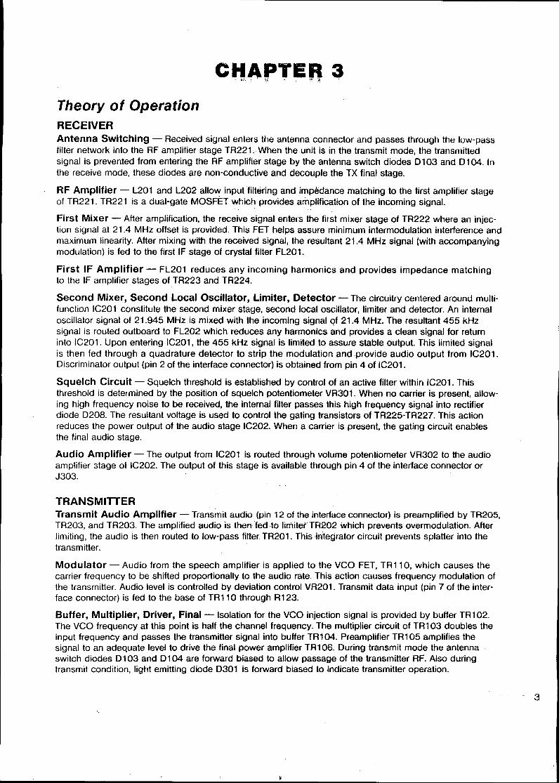
Theory of OperationRECEIVERAntenna Switching - Received signal enters the antenna connector and passes through the low-passfiller network into the RF amplifier stage TR221. When theunit is in the transmit mode, the transmittedsignal is prevented from entering the RF amplifier stage by the antenna switch diodes 0103 and 0104. Inthe receive mode, these diodes are non-conductive and decouple the TX final stage.
RF Amplifier - L201 and L202 allow inputfiltering and impedance matching to the first amplifier stageof TR221. TR221 is a dual-gate MOSFET which provides amplification of the incoming signal.
First Mixer - After amplification, the receive signal enters the first mixer stage of TR222 where an injec-tion signal at 21.4 MHz offset is provided. This FET helps assure minimum intermodulation interference andmaximum linearity. After mixing with the received signal, the resultant 21.4 MHz signal (with accompanyingmodulation) is fed to the first IF stage of crystal filter FL201.
First IF Amplifier - FL201 reduces any incoming harmonics and provides impedance matchingto the IF amplifier stages of TR223 and TR224.
Second Mixer, Second Local Oscillator, Limiter, Detector - The circuitry centered around multi-function IC201 constitute the second mixer stage, second local oscillator, limiter and detector. An internaloscillator signal of 21.945 MHz is mixed with the incoming signal Qf 21.4 MHz. The resultant 455 kHzsignal is routed outboard to FL202 which reduces any harmonics and provides acıean signal for returninto IC201. Upon entering IC201, the 455 kHz signal is limited to assure stable output. This limited signalis the n fed through a quadrature detector to strip the modulation and provide audio output from IC201.Oiscriminator output (pin 2 of the interface connector) is obtained from pin 4 of IC201.
Squelch Circuit - Squelch threshold is established by control of an active filter within IC201. Thisthreshold is determined by the position of squelch potentiometer VR301. When no carrier is present, allow-ing high frequency noise to be received, the internal filter passes this high frequency signal into rectifierdiode 0208. The resultant voltage is used to control the gating transistors of TR225-TR227. This actionreduces the power output of the audio stage IC202. When a carrier is present, the gating circuit enablesthe final audio stage.
Audio Amplifier - The output from IC201 is routed through volume potentiometer VR302 to the audioamplifier stage of IC202. The output of this stage is available through pin 4 of the interface connector orJ303.
TRANSMITTERTransmit Audio Amplifier - Transmit audio (pin 12 of the intertace connector) is preamplified by TR205,TR203, and TR203. The amplified audio is then fed to liffiitet TR202 iNhich prevents overmodulation. Afterlimiting, the audio is then routed to low-passfilter. TR201. This ,integrator circuit prevents splatter into thetransmitter.
Modulator - Audio from the speech amplifier is applied to the VCO FET, TRll0, which causes thecarrier frequency to be shifted proportionally to the audio rate. This action causes frequency modulation ofthe transmitter. Audio level is controlled by deviation control VR201. Transmit data input (pin 7 of the inter-face connector) is fed to the base of TR110 through R123.
Buffer, Multiplier, Driver, Final-Isolation for the VCO injection signal is provided by buffer TR102.The VCO frequency at this point is half the channel frequency. The multiplier circuit of TRl 03 doubles theinput frequencyand passes the transmitter signal into buffer TR104. Preamplifier TR105 amplifies thesignal to an adequate level to drive the final power amplifier TR106. During transmit mode the antennaswitch diodes 0103 and 0104 are forward biased to allow passage of the transmitter RF. Also duringtransmit condition, light emitting diode 0301 is forward biased to indicate transmitter operation.
- 3
4
SYNTHESIZERThe primary function of the synthesizer is to provide transmitter injection signal, and local asciIIatar signalto the receiver. This design allows a single crystal oscillator to provide stable frequency generation withoutthe need for tuning crystals for each channel. By dividing the reference oscillator signal by an amountrespective of the selected channel, the synthesizer can provide a range of frequencies.
Programming of the synthesizer is accomplished via the diode matrix board, located at the back of the unit.Tlıese diodes determine the proper divide ratio for the synthesizer. (Refer to diode programming instruc-tions in chapter 4.)
The design used in the SP-605HffM is a premix PLL configuration which allows a lower frequencyoutputfrom the VGü. This is desired to allow accurate division by the digital divider circuitry.
Voltage Controlled Oscillator (VCO) - The VGü consists of oscillator TR11 O and varactor diode0106. The effective capacitance of 0106 is controlled by the OC tuning voltage. As the tuning valiage ischanged, the oscillator frequency of the VGü follows. The output of the VGü is applied to the doublercircuits of TR101 and TR103. TR101 feeds the receiver, and TR103 provides signal into the transmitter.The VGü output is alsa applied to cascaded buffer stages TR111 and TR112 which feed the mixer circuitfor the phased-Iocked-Ioop (PLL).
Pre-Mix Local Oscillator - In order to reduce the VGü to a frequency suitable for division by the lowspeed logic, the VGü output is mixed with the output of the oscillator/doubler TR115. In the receive mode,the VGü output must be offset from the transmit frequency by half of the first IF frequency. This, and asemi-duplex split is accornplished by using a different crystal frequency at the pre-mix oscillator.
Mixer and Low Pass Filter - The mixer circuit of TR113 mixes the VGü frequency with the output ofthe pre-mix asciIIatar TR115. The desired resultant, which is the difference frequency (or lower frequencycomponent) is passed by the low pass filter consisting of GH1OB, G177, and G17B.
Pre-Mix Local Oscillator - In order to reduce the VGü to a frequency suitable for division by the low .speed logic, the VGü output is mixed with the output of the oscillator/-':~'lbler TR115. In the receive mode,the VGü output must be offset from the transmit frequency by half of the first IF frequency. This, and aserni-duplex split is accomplished by using a different crystal frequency at the pre-mix oscillator.
Oivider Buffer - The output of the low pass filter is buffered and amplified by TR114 to the level reqiredby programmable divider IG101.
Programmable Oivider - Oivision of the buffered pre-mix output is accomplished by programmabledivider IG101. The division ratio is set by the programming diodes on the diode matrix board. This divisionprocess determines the output of the VGü. ._
Phase Comparator, Reference Oscillator/Oivider"":- By comparing the divided VGü frequency tothe reference oscillator, the synthesizer can determine if the VGü is on the proper operating frequency, asdetermined by the programming diodes. If a difference is detected, the OG tuning voltage will be changedto drive the VGü to the correct outpul.
The DG tuning voltage is derived from the fillered ou~put ofphase comparalar IC103. üutput from IG103represents the difference between the divided output of. programmable divider IC1 01, and the 2.5 kHzoutput from the reference oscillator/di~ider IC1 02,. The 2.5 kHz refere0ce signal is derived from the10.240 Mhz reference oscillator and a fixed division ratio in the. referance divider of 4096. Any detecteddifference will alter the OC tuning voltage to bring the VCü output to the correct frequency.
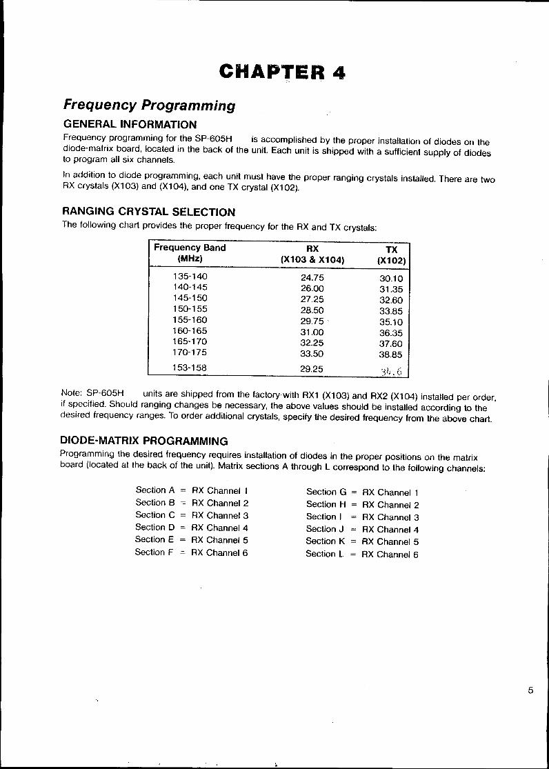
CHAPTER 4Frequency ProgrammingGENERAL INFORMATIONFrequency programming for the SP-605H is accomplished by the proper installation of diodes on thediode-matrix board, located in the back of the uniL.Each unit is shipped with a sufficient supply of diodesto program all six channels.
In addition to diode programming, each unit must have the proper ranging crystals installed. There are twoRX crystals (X103) and (X104), and one TX crystal (X102).
RANGING CRYSTAL SELECTIONThe following chart provides the proper frequency for the RX and TX crystals:
Frequency Band RX TX(MHz) (X103 & X104) (X102)
135-140 24.75 30.10140-145 26.00 31.35145-150 27.25 32.60150-155 28.50 33.85155-160 29.75 . 35.10160-165 31.00 36.35165-170 32.25 37.60170-175 33.50 38.85153-158 29.25 34.6
Note: SP-605H units are shipped from the factorywith RX1 (X103) and RX2 (X104) installed per order,if specified. Should ranging changes be necessary, the above values should be installed according to thedesired frequency ranges. To order additional crystals, specify the desired frequency from the above charto
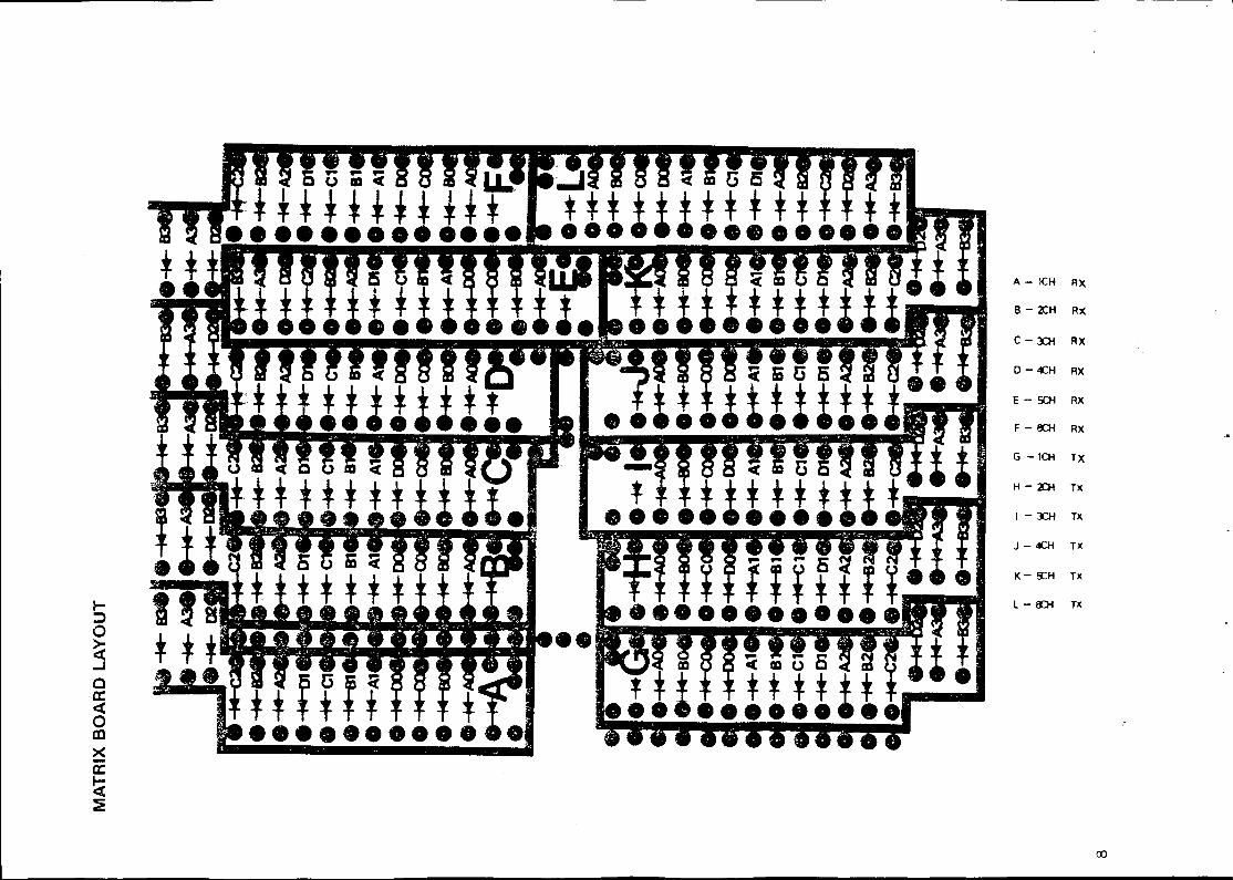
DIODE-MATRIX PROGRAMMINGProgramming the desired frequency requires installation of diodes in the proper positions on the matrixboard (Iocated at the back of the unit). Matrix sections A through L correspond to the following channels:
Section A RX Channel1 Section G = RX Channel 1Section B RX Channel2 Section H RX Channel2Section C RX Channel3 Section i RX Channel3Section D RX Channel4 Section J RX Channel4Section E RX Channel 5 Section K RX Channel 5Section F RX Channel6 Section L RX Channel6
5
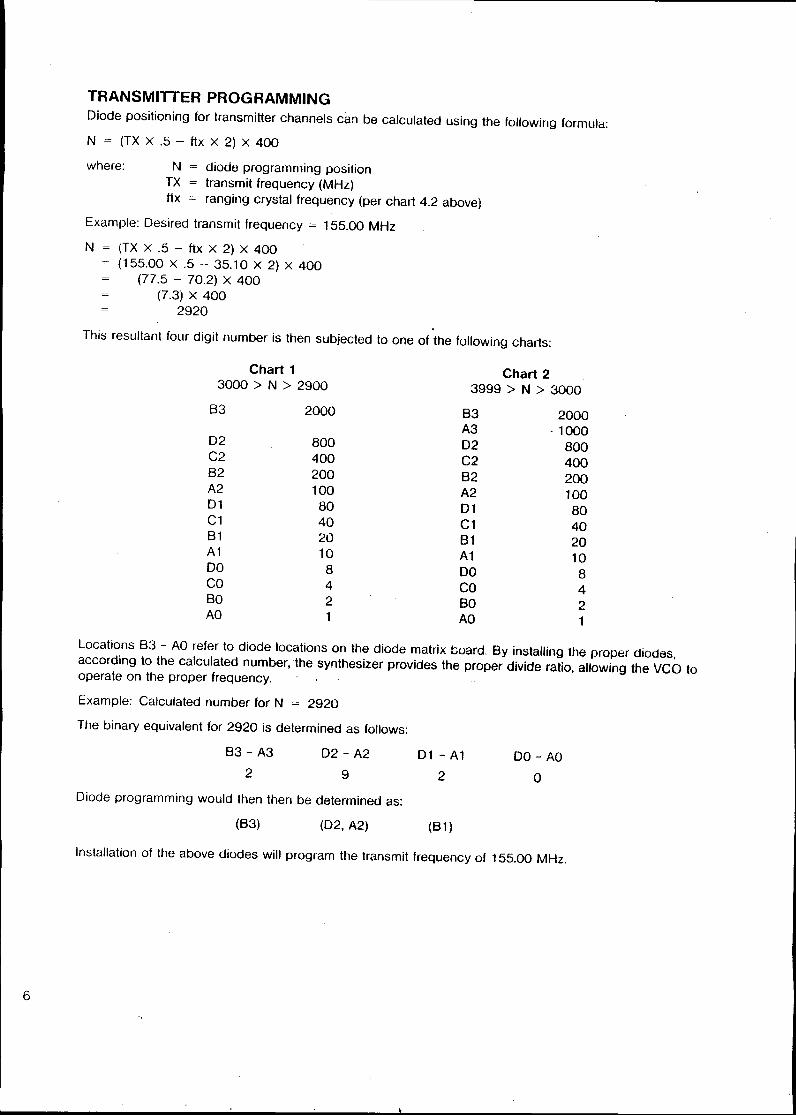
where:
TRANSMIITER PROGRAMMINGDiode positioning for transmitter channels can be calculated using the following formula:
N = (TX X .5 - ftx X 2) X 400
N diode programming positionTX = transmit frequency (MHz)ftx = ranging crystal frequency (per chart 4.2 above)
Exarnple: Desired transmit frequency = 155.00 MHz
N (TX X .5 - ftx X 2) X 400(155.00 X .5 - 35.10 X 2) X 400
(77.5 - 70.2) X 400(7.3) X 400
2920
This resultant four digit number is then subjected to one of the following charts:
Chart 1 Chart 23000 > N > 2900 3999 > N > 3000B3 2000 B3 2000
A3 .1000D2 800 D2 800C2 400 C2 400B2 200 B2 200A2 100 A2 100D1 80 D1 80C1 40 C1 40B1 20 B1 20A1 10 A1 10DO 8 DO 8CO 4 CO 4BO 2 BO 2AO 1 AO 1
Locations B3 - AO refer to diode locations on the diode matrix board. By installing the proper diodes.according to the calculated number, the synthesizer provides the proper divide ratio, allowing the VCü tooperate on the proper frequency.
Example: Calculated number for N = 2920
The binary equivalent for 2920 is determined as follows:
B3 - A3
2D2 - A2
9D1 - A1
2DO - AO
ODiode programming would then then be determined as:
(B3) (D2, A2) (B1 )
6
Installation of the above diodes will program the transmit frequency of 155.00 MHz.
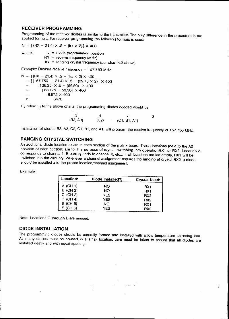
where:
RECEIVER PROGRAMMINGProgramming of the receiver diodes is similar to the transmitter. The only diHerence in the procedure is theapplied formula. For receiver programming the following formula is used:
N = [(RX - 21.4) X .5 - (frx X 2) i x 400
N diode programming positionRX = receive frequency (MHz)frx = ranging crystal frequency (per chart 4.2 above)
Example: Desired receive frequency = 157.750 MHz
N [(RX - 21.4) x .5 - (frx X 2) X 400[(157.750 - 21.4) X .5 - (29.75 X 2) i X 400
[(136.35) X .5 - (59.50») X 400[68.175 - 59.50) X 400
8.675 X 4003470
8y referring to the above charts, the programming diodes needed would be:
3(83, A3)
4(C2)
7(C1, 81, A1)
O
Installation of diodes 83, A3, C2, C1, 81, and A1, wili program the reeeive frequency of 157.750 MHz.
RANGING CRYSTAL SWITCHINGAn additional diode location exists in each section of the matrix board. These locations (next to the AOposition of each section) are for the purpose of crystal switching into operationRX1 or RX2. Location Acorresponds to channel 1; 8 corresponds to ehannel 2, ete ... If all locations are left empty, RX1 will beswitched into the eircuitry. Whenever a channel assignment requires the ranging of erystal RX2, a diodeshould be installed into the proper loeation/ehannel assignment.
Example:
Location:
A (CH 1)8 (CH 2)C (CH 3)D (CH 4)E (CH 5)F (CH 6)
Note: Locations G through L are unused.
Diode Installed?:
NONOYESYESNOYES
Crystal Used:
RX1RX1RX2RX2RX1RX2
OIOOE INSTALLATIONThe programming diodes should be earefully formed and installed with a low temperature soldering iron.As many diodes must be housed in a smail location, care must be taken to assure that all diodes areinstalled neatly and with equal spacing.
7
•••:::Jo~..Joa:«oaı~a:~~
*.*ff*****••••••••••••
A - lCH RX
B - 2CH Rı(
c-:nı RX
0- 4CH RX
E - 5Qi RX
F - OC:H RX
G -101 TX
H - 2CH Tx
i -:l:H TX
J - 4CH nı
K -!:CH Tx
L - OC:H T>ı
ro
CHAPTER 5.' "'~ .~~ :ı.:}~
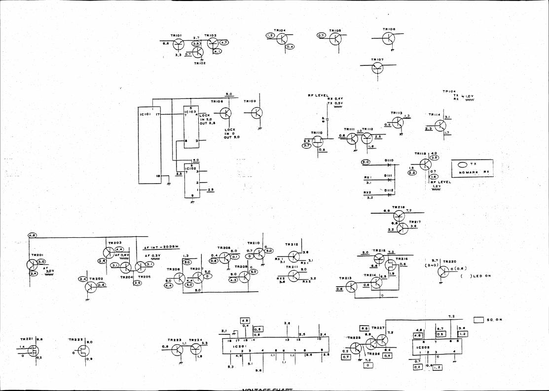
A/ignment ProceduresPRELlMINARYAlignment of the SP-605H should be performed by qualified technicians only. Warranty may be void iftechnical repair is attempted by anyone that is not trained and famiHar with portable communicationsequipmenL.
Alignment of the SP-605H can easily be accomplished with standard test equipment. However, theequipment should be within calibration standards to assure accurate alignment of the radio equipmenL.
PHASE-LOCKED LOOP (PLL)Connect an oscilloscope to TP101 and adjust L118 for maximum signal (in receive mode) at this poinL.Once this is accomplished, turn the core of the coil dow n one turn to broaden the adjustmenl. (Thisadjustment should be accomplished on the lowest frequency that the unit is programmed to operate.)
With the unit on the lowest programmed receive frequency, connect a DC voltmeter to TP1 03 (top of R120)and adjust L114 for 1.28 VDC. Connect a wattmeter to the antenna jack. Then key the transmitter on thelowest frequencyand increase this voltage until the transmit power appears.
Connect an oscilloscope to TP104 and adjust L119 for 1.0 to 1.6 volts peak-to-peak in the transmit mode.After this adjustment, recheck the DC voltage at TP1 03 to assure that the voltage is less than 3.0 VDC inthe transmit mode. If the reading is greater, perform the above procedure for L114 again.
Canneel a frequency counter to TP105 and adjust the following variable capacitors to obtain the properfrequency (+ /- 200 Hz) according to the following calculation:
RX == (Fo - 21.4) X .5TX == Fo X .5
Where Fo == selected frequencyFor frequencies in the lower 5 MHz receive band, adjust VC1 07 to obtain the proper frequency.For frequencies in the upper 5 MHz receive band, adjust VC108 to obtain the proper frequency.For frequencies in the upper 3 MHz transmit band, adjust VC1 06 to obtain the proper frequency.
RECEIVER ALlGNMENTLocal Oscillator - Connect an RF voltmeter to the source of receiver mixer TR222. Adjust L10 1 andL102 for maximum leveJ. If an RF voltmeter is not available, L101 and L102 can be adjusted for bestSINAD while feeding a high level, on-channel signal to the receiver.
Receiver Front-End Alignment - Input an on-channel signal into the receiver and adjust L201-L204for best SINAD. (This adjustment should be startoo on the center frequency of the programmed channels.After setting L201-L204, the outside channels should be checked for proper specifications. if outside thespecified limits, readjust L201-L204 for proper readings.)
IF/Detector Alignment - These circuits ~re normally factory tuned and should not be retuned unlessabsolutely necessary. If retuning is required, adjust L205 and L2Ö6 for best SINAD.
, '- .' ,. . "- .Squelch Threshold Adjustment -Connect"asignal generatar to the receiver and modulate theselected frequency with a 1 kHz tane, set. for 3.3. kHz deviatian. Set the ouptut level of the generatar at0.25,N. Adjust the squelch control to maximum squelch pasition and adjust VR202 to open squelch. Afteradjustment, remove the input signal to the receiver and rotate the squelch control to assure that the radio issquelched within the first quarter turn of the control.
9
TRANSMITTER ALlGNMENTPreliminary - Connect a wattmeter of suitable range to the antenna connector. Adjust VC104 andVC105 to mid-position. Check air coils LL06, ll08, and III O, to assure that non e of the coils are shorted.
Transmitter Buffer Alignment - Set the channel selector to center frequency of the programmedfrequencies. Connect a OC voltmeter to TP102 and adjust Ll 03 and Ll 04 to peak vollage reading intransmit mode. (Continue this procedure until maximum vollage is obtained. However, the cores should notbe above the top of thecans. If this occurs, resetthe cores to mid"'position and readjust.) Adjust VC10l tomaximum voltage at TP102. Retrim adjustments l1 03, LL04, and VC10l to obtain maximum vollage.
Driver and Final Power AMP Alignment - Activate the transmitter on the radio's center frequencyand adjust VC102, VC103, VC104, and VC105, for maximum power output. If power output degrades onoutside channels, decrease VC105 (slightly) and retune VCl 02-VCl 04.
"LO" Power Setting Adjustment - Set the "lA" power switch (SW301) to the lA position andadjust VR10l to the desired output (factory set for 1 watt).
Modulator Alignment - Set the transmitter in the "HI" position and modulate the transmitter. AdjustVR20l for 4.8 kHz of deviation. Check the "LO" power setting to assure that the modulation remainsthe same.
Power Supply Check - To assure proper operation, the SP-605HITM should not exceed the followingcurrent drain specifications:
ModelSP-605hSP-605HSP-605H
Supply Voıtage12.0 VDC12.0 VDC12.0 VDC
ModeTX "HillTX"lO"RX
Maximum Current1.2 A
450 mA90 mA
In the event that current drain is substantially greater than the above values, the unit should be retunedand/or checked for defect.
CHAPTER 6-""- ~'t .. ~- ., {~-'i '"c-' • !.~;' : :",i "
"
Parts ListGENERAL INFORMATIONThe schematics in Chapter 8 incorporate all component values along with the schematic identificationnumber. These values, or manufacturer part numbers, should be used when replacing defactive parts.
ORDERING INFORMATIONWhen ordering replacement parts from the factory,simply use the following nomenelature:
Example:
ModelSP-605H
Schematic Identlficatlon
TR106
10
This part number would coordinate to the final transistor (TR106) in the transmitter of a model SP-60SH/Any changes in component values or manufacturer's part numbers will be coordinated at the factory to
assure that the proper part is replaced.

CHAPTER .,,'O ~' ,:.... "
OptionsSINGlE TONE CTCSS ENCODER/DECODER (PT-10l)
Tone Data Chart
Tone Freq. DataTone # (Hz) DO 01 02 03 04 05
1 67.0 1 1 1 1 1 12 71.9 1 1 1 1 1 O3 74.4 O 1 1 1 1 14 77.0 1 1 1 1 O O5 79.7 1 O 1 1 1 16 82.5 O 1 1 1 1 O7 85.4 O O 1 1 1 18 88.5 O 1 1 1 O O9 91.5 1 1 O 1 1 110 94.8 1 O 1 1 1 O11 97.4 O 1 O 1 1 112 100.0 1 O 1 1 O O13 103.5 O O 1 1 1 O14 107.2 O O 1 1 O O15 110.9 1 1 O 1 1 O16 114.8 1 1 O 1 O O17 118.8 O 1 O 1 1 O18 123.0 O 1 O 1 O O19 127.3 1 O O 1 1 O20 131.8 1 O O 1 O O21 136.5 O O O 1 1 O22 141.3 O O O 1 O O23 146.2 1 1 1 O 1 O24 151.4 1 1 1 O O O25 156.7 O 1 1 O 1 O26 162.2 O 1 1 O O O27 167.9 1 O 1 O 1 O28 173.8 1 O 1 O O O29 179.9 O O 1 O 1 O30 186.2 O O 1 O O O31 192.8 1 1 O O 1 O32 203.5 1 1 O O O O33 210.7 O 1 O O 1 O34 218.1 O 1 O O O O35 225.7 1 O O O 1 O36 233.6 1 O O O O O37 241.8 O O O O 1 O38 250.3 O O O O O O
Switch Settings VR 701
0 OFF= ıdo 02 04
~ ~ ~
ON= oc c
01 03 05
Tone Encode Level Adjust - Key transmitter and adjust VR701 for 500 - 575 Hz CTÇSŞ t9n~ ..devialion. (Check aıı frequencies and average accordingly.)
1
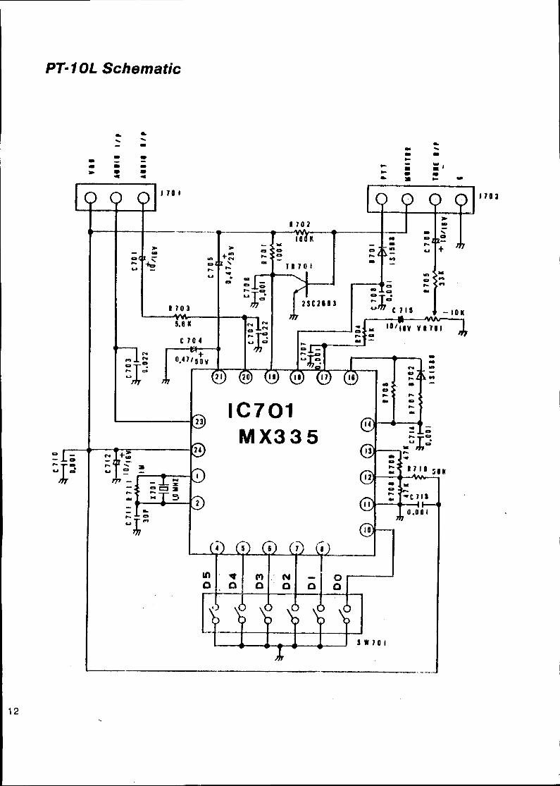
PT-10L Schematic
-1011
••..•...onco...••
••-... •••co... •••••...co•..•••• o~TC::
w ".,0•....
IO/lly YIJOI
••ct•...••
..ol .•.• ••..
~ • ;,t- • •~ :ıl •.. ••
nu
•• o
:T~•...m c 715
wca
1702
iO ilw
o o•... o
•• Tl 7 O i
IC701MX335
:>
+~,•......ca
LI>CO•......•
i 7 O 3
5.811
C 7 04
+0.47/50V
•...••
.•.o
...:i~•.•• co...•
•......•
~ ...•. .•.•
• ••• • •»- • •4 ••J 70 i
•••....,r.•..•Ar cl
oQ
s W J O i
12


![[Clarinet_Institute] d'Indy Chanson Danses Fl Ob 2Cl 2Bsn Hn](https://static.fdocuments.us/doc/165x107/56d6be291a28ab301690e9a3/clarinetinstitute-dindy-chanson-danses-fl-ob-2cl-2bsn-hn.jpg)

![[Clarinet_Institute] Irsen Sonatine 2Cl](https://static.fdocuments.us/doc/165x107/577c7af41a28abe05496a9e9/clarinetinstitute-irsen-sonatine-2cl.jpg)


