© 2014 Chris Edwards
142
© 2014 Chris Edwards
Transcript of © 2014 Chris Edwards

© 2014 Chris Edwards

DIFFRACTION PHASE MICROSCOPY FOR APPLICATIONS IN MATERIALS SCIENCE
BY
CHRISTOPHER ADAM EDWARDS
DISSERTATION
Submitted in partial fulfillment of the requirements for
the degree of Doctor of Philosophy in Electrical and Computer Engineering
in the Graduate College of the
University of Illinois at Urbana-Champaign, 2014
Urbana, Illinois
Doctoral Committee:
Associate Professor Lynford Goddard, Chair
Associate Professor Gabriel Popescu
Professor Brain Cunningham
Professor Stephen Boppart

ii
Abstract
Quantitative phase imaging (QPI) is a flourishing new field which has recently found
tremendous success in the life sciences. QPI utilizes not only the amplitude of the imaging field,
but also its phase, in order to provide quantitative topographical and/or refractive index data. As
fields from the source interact with the specimen, a fingerprint of the sample’s structure is
encoded into the phase front of the imaging field, which can then be used to reconstruct a map of
the sample’s surface at the nanoscale. Unfortunately, cameras and detectors only respond to
intensity. For this reason, a wide variety of QPI techniques have been developed over the years
in order to gain access to this valuable phase information.
Diffraction phase microscopy (DPM) utilizes a compact Mach-Zehnder interferometer to
combine many of the best attributes of current QPI methods. This compact configuration is
common-path which inherently cancels out most mechanisms responsible for noise and is single-
shot meaning that the acquisition speed is limited only by the speed of the camera employed.
This technique is also non-destructive and does not require staining or coating of the specimen.
This unique collection of features enables the DPM system to accurately monitor the dynamics
of various nanoscale phenomena in a wide variety of environments. Our DPM system has been
used to monitor wet etching, photochemical etching, dissolution of biodegradable electronic
materials, expansion and deformation of thin-films and microstructures, and surface wetting and
evaporation. It has also been used in semiconductor wafer defect detection.
Imaging systems using white light illumination can exhibit up to an order of magnitude lower
noise than their laser counterparts. This is a result of the lower coherence, both spatially and
temporally, which reduces noise mechanisms such as laser speckle. Unfortunately, white light

iii
systems also exhibit additional object-dependent artifacts, like the well-known halo effect, that
are not present in their laser counterparts. Recently, we have shown that such artifacts are due to
a high-pass filtering phenomenon caused by a lack of spatial coherence. This realization allowed
us to quantitatively model the phase reductions and halo effect, and remove them using a variety
of techniques.
The final DPM/wDPM system is capable of providing halo-free images of structures typical
in both materials and life science applications and operates in both transmission and reflection
modes in order to accommodate both transparent and opaque samples alike. The DPM/wDPM
system can be implemented as an add-on module that can be placed at the output port of any
conventional light microscope. The user can easily switch between laser and white light sources,
as well as transmission and reflection, simply by flipping switches on the microscope.
Furthermore, the spatial coherence for white light DPM (wDPM) can be optimized for the given
application by rotating the condenser turret in transmission, or adjusting the slider for the
aperture diaphragm in reflection, which contain different size pinholes, allowing for a tradeoff
between accuracy and speed. The setup also includes an automatic pinhole alignment system,
real-time phase imaging, and a graphical user interface (GUI) to make it as user-friendly as
possible. The final system was built in the Imaging Suite in Beckman Institute for Advanced
Science and Technology to serve as a multi-user inspection/characterization tool that will create
a major pipeline for high-impact projects and publications in a variety of fields.

iv
TABLE OF CONTENTS
LIST OF ACRONYMS ............................................................................................................... vi
CHAPTER 1: INTRODUCTION ................................................................................................ 1
1.1 Early Microscopy ................................................................................................................................ 1
1.2 Holography ......................................................................................................................................... 2
1.3 Quantitative Phase Imaging ................................................................................................................ 3
1.4 Diffraction Phase Microscopy ............................................................................................................ 5
1.5 Other Imaging Techniques .................................................................................................................. 6
1.6 Dissertation Overview ........................................................................................................................ 9
CHAPTER 2: DIFFRACTION PHASE MICROSCOPY: DESIGN, OPTIMIZATION,
AND IMPLEMENTATION ....................................................................................................... 11
2.1 Theory ............................................................................................................................................... 11
2.2 Design Principles .............................................................................................................................. 15
2.3 Phase Reconstruction ........................................................................................................................ 26
2.4 Noise Characterization and System Verification .............................................................................. 31
CHAPTER 3: DIFFRACTION PHASE MICROSCOPY FOR MATERIALS SCIENCE
APPLICATIONS ........................................................................................................................ 33
3.1 Watching Semiconductors Etch ........................................................................................................ 33
3.2 Digital Projection Photochemical Etching ........................................................................................ 39
3.3 Dissolution of Biodegradable Electronics ......................................................................................... 49
3.4 Expansion and Deformation of Materials ......................................................................................... 53
3.5 Surface Wetting and Evaporation ..................................................................................................... 62
3.6 Defect Detection in Semiconductor Wafers ...................................................................................... 76
CHAPTER 4: DIFFRACTION PHASE MICROSCOPY WITH BROADBAND
ILLUMINATION ....................................................................................................................... 80
4.1 Setup, Design, and Processing .......................................................................................................... 80
4.2 Temporal and Spatial Coherence ...................................................................................................... 83
4.3 Image Formation ............................................................................................................................... 89
4.4 Halo Removal ................................................................................................................................. 102
CHAPTER 5: CONCLUSIONS .............................................................................................. 110

v
5.1 Final System.................................................................................................................................... 110
5.2 Deployment ..................................................................................................................................... 119
5.3 Final Conclusions ............................................................................................................................ 122
REFERENCES .......................................................................................................................... 124

vi
LIST OF ACRONYMS
1D, 2D, 3D one-, two-, three-dimensional
AFM atomic force microscopy
BPF band-pass filter
CCD charge-coupled device
CMOS complementary metal–oxide–semiconductor
CUDA compute unified device architecture
DHM digital holographic microscopy
DPM diffraction phase microscopy
epi-DPM epi-illumination diffraction phase microscopy
epi-wDPM epi-illumination white-light diffraction phase microscopy
FOV field of view
FPM Fourier phase microscopy
GUI graphical user interface
HPF high-pass filter
HPM Hilbert phase microscopy
IDA intentional defect array
LED light-emitting diode
LPF low-pass filter
MPM multi-photon microscopy
NA numerical aperture
NIR near-infrared
NSIM non-linear structured illumination microscopy

vii
NSOM near-field scanning optical microscopy
OTF optical transfer function
PALM photoactivated localization microscopy
PR photoresist
PSF point spread function
PSI phase shifting interferometry
QPI quantitative phase imaging
QWLSI quadriwave lateral shearing interferometry
RGB red-green-blue
SCL supercontinuum laser
SEM scanning electron microscopy
SIM structured illumination microscopy
SLIM spatial light interference microscopy
SLM spatial light modulator
SNR signal to noise ratio
SRC Semiconductor Research Corporation
SSIM saturated structured illumination microscopy
STED stimulated emission depletion
STM scanning tunneling microscope
STORM stochastic optical reconstruction microscopy
SWLI scanning white light interferometry
TEM transmission electron microscopy
TIRF total internal reflection fluorescence microscopy
wDPM white light diffraction phase microscopy

1
CHAPTER 1: INTRODUCTION
1.1 Early Microscopy
Antonie van Leeuwenhoek (1632-1723) is commonly identified as “the Father of Microbiology”
[1]. He began working as a cloth merchant at the age of 16 and later opened his own shop in
1654. It was during this time that he developed a passion for grinding and polishing his own
lenses, which were originally used to quantify thread counts [2]. He soon began building his own
personal compound microscopes with magnifications far exceeding those available at the time.
In fact, it is reputed that his miniature microscopes, only a few cm in size, must have possessed
up to 300X the magnification of their competitors [1]. His innate curiosity allowed him to be the
first person in recorded history to peer into a microscope and discover a new and exciting realm
of existence, one teeming with microscopic life [2]. In an era rife with pseudo-scientific
speculation, his letters published by the Royal Society marked the birth of microbiology and
helped to jump-start the modern field of light microscopy [1, 2].
Resolution and contrast provided the two major bottlenecks which hindered early
development in the field [1, 2]. Early studies focused primarily on biological specimens, which
are often optically thin and transparent. As a result, improving contrast was the motivating force
behind the development of new techniques. However, early development was stymied by a
primitive understanding of imaging theory. Despite the production of higher and higher
magnification lenses, it was soon realized that a limit existed regarding the smallest observable
structure. It was not until a hundred years later, in 1873, that German physicist Ernst Abbe
(1840-1905) used wave optics to derive the hard limit on image resolution and successfully

2
modeled image formation as the interference betweem scattered and unscattered light [2, 3]. In
1936, Dutch physicist Frits Zernike (1888-1966) was then able to build from this theory, the
phase contrast technique, which introduces a phase shift between the scattered and unscattered
components causing the phase information to be mapped into the amplitude [2, 4]. The human
eye, as an optical detector, only responds to intensity, so this was the first time that phase
information could be observed in microscopy [2, 5]. This invention would later earn him a Nobel
Prize in 1953. Other contrast enhancement techniques such as differential interference contrast
(DIC or Normarski) [2, 3] were also developed. Although these new methods provided drastic
improvement to the image contrast for particular samples, the information was still only
qualitative.
1.2 Holography
In 1948, Hungarian-British physicist, Dennis Gabor, introduced the concept of holography: the
process by which a recording of the field scattered by an object is encoded onto a photographic
plate such that a virtual image of the object can be reproduced in a different place, at a different
time, without the original object being present [6]. Unfortunately, due to a lack of coherent light
sources at the time, holography did not gain popularity until after the invention of the laser in
1960.
With high coherence sources available, holographic techniques became more practical and
found applications in a variety of fields [7]. The Shack-Hartmann wavefront sensor (SHWFS)
was developed is the 1960s and consists of a 2D array of identical and equally spaced lenses
focused on a CCD camera, which allows for reconstruction of the impingent wavefront by
measuring local variations in the focal spot coming from each lens [2]. This sensor was initially

3
used to characterize the atmosphere’s optical transfer function (OTF) in astronomical
measurements and later to measure surface profiles and characterize the quality of laser beams
and surface roughness of various materials. Significant advances in the development and
commercialization of holographic technologies for optical testing such as computer-generated
holography, phase-shifting interferometery (PSI), and scanning white light interferometery
(SWLI) appeared in the 1980s and 90s led by Wyant and his colleagues [8, 9].
1.3 Quantitative Phase Imaging
Although digital holography was suggested back in the 1960s, it was not until the mid-1990s that
advances in digital image sensors and computers allowed holograms to be recorded on charge-
coupled devices (CCDs) and reconstructed with adequate quality, entirely in software [10-13].
Following the turn of the millennium, scientific-grade CCDs and complementary metal-oxide-
semiconductor (CMOS) cameras became available at reasonable prices. Such advances resulted
in the development of an exciting new field, quantitative phase imaging (QPI), which has
become a ubiquitous inspection/characterization tool in biomedical studies [3]. QPI techniques
are generally non-invasive and label-free, which means there is no need for fluorescence dyes or
markers, making them ideal for live biological imaging [3]. In fact, it has been used to study cell
dynamics [3, 14, 15] and growth [16-21], as well as blood testing [22, 23] and even 3D imaging
[24-26]. QPI utilizes both the amplitude and phase of the imaging field in order to provide
quantitative topographical and/or refractive index data. As fields from the source interact with
the specimen, a fingerprint of its structure is encoded into the phase front, which can then be
used to reconstruct a map of the sample’s surface at the nanoscale [27-29]. Optical frequencies
contained within the visible spectrum are far too rapid for conventional electronic-based sensors

4
like charge-coupled devices (CCDs) and photodetectors to track the phase directly. Instead, what
is recorded is a time average over many cycles, averaging out the phase, and leaving only the
field intensity. Thus, various QPI techniques have been developed in order to gain access to this
valuable phase information.
A myriad of approaches to QPI have been developed over the years and are best described by
the following classifiers: common-path, phase-shifting, off-axis, and white light interferometry,
each with their own unique set of strengths and weaknesses [2]. Common-path approaches are
renowned for their robustness and stability. Since both interferometer arms traverse the same
optical components and therefore significantly overlap in space and time, the noise in one arm is
highly correlated with that of the other, thereby cancelling each other out in the final phase
measurement. Fourier phase microscopy (FPM) [26] and spatial light interference microscopy
(SLIM) [30], as well as spiral phase contrast [14], quadriwave lateral shearing interferometry
(QWLSI ) [31], and even transport of intensity [32] are popular common-path QPI approaches.
Phase-shifting interferometry employs temporal phase modulation, which allows for a common-
path geometry, but requires multiple raw images (three or more) in order to reconstruct a single
phase image [33, 34]. Initially, this made the approach impractical for high-speed dynamics, but
recent advances have yielded an order of magnitude improvement to the acquisition speed [14].
Off-axis methods, on the other hand, perform the modulation spatially, which produces a single
phase image for every raw image collected and are therefore better suited for high-speed
dynamics. Most conventional digital holography microscopy (DHM) methods utilize this
approach [18]. Off-axis methods, however, generally suffer from higher noise floors, with the
exception of diffraction phase microscopy (DPM) which elegantly combines the off-axis
approach with a common-path geometry.

5
1.4 Diffraction Phase Microscopy
DPM combines many of the best attributes of current QPI techniques in a very efficient manner
[35-40]. The term diffraction comes from the fact that a diffraction grating along with a 4f lens
system, pinhole filter, and CCD camera are used to form a compact Mach-Zehnder
interferometer and achieve interference. This compact, off-axis approach benefits from both the
low spatiotemporal noise and fast acquisition speeds of previous QPI techniques. Furthermore, it
does not require staining or coating of the specimen as is thus non-destructive. This unique
collection of features enables the DPM system to study a variety of interesting phenomena at the
nanoscale in their natural environments. Our DPM system is currently being used to monitor wet
etching [41, 42], photochemical etching [42], dissolution of biodegradable electronic materials
[42, 43], expansion and deformation of thin-films and microstructures [44], surface wetting and
microdroplet evaporation [45, 46]. A separate DPM system was also built and is being used for
defect detection in semiconductor wafers [47-49].
A variety of laser sources both in the visible and infrared (IR) regimes have been used to
perform quantitative phase imaging [47-51]. More recently, broadband techniques using super-
continuum lasers (SCLs), light emitting diodes (LEDs), and even standard halogen lamp
illumination have been demonstrated [52, 53]. As a result of their lower coherence (both
temporally and spatially) which reduces several noise mechanisms including laser speckle, white
light methods generally provide a better signal-to-noise ratio (SNR). On the other hand, if not
treated properly, the low spatial coherence also introduces object-dependent artifacts such as
halos, which disrupt the quantitative measurements [14, 15, 19, 54, 55]. Both the temporal and
spatial coherence of the source can be accessed via direct measurements of the spectrum and

6
should be characterized in order to ensure adequate coherence for a given type of interferometry
[14, 55, 56]. In general, the temporal coherence length must exceed the largest optical pathlength
difference and the mutual intensity function must be flat over the object being measured, or
ideally, the entire field of view [2].
1.5 Other Imaging Techniques
High-resolution imaging systems like the scanning electron microscope (SEM) and transmission
electron microscope (TEM) were developed in the 1930s [2, 55, 57]. The scanning tunneling
microscope (STM) and atomic force microscope (AFM) were developed in the 1980s [58, 59].
Since the 1980s, several other super-resolution techniques were developed in an attempt to
surpass the diffraction limit [60, 61], some of which include near-field scanning optical
microscopy (NSOM), multi-photon microscopy (MPM), stimulated emission depletion
microscopy (STED), structured illumination microscopy (SIM), stochastic optical reconstruction
microscopy (STORM), and photoactivated localization microscopy (PALM).
The scanning electron microscope produces images by raster scanning the sample with a
focused beam of electrons. The electrons interact with charged particles in the sample producing
a signal which contains high-resolution (< 1 nm) information about the surface topography [62].
In order for SEM to produce high contrast images, the sample must possess a certain degree of
conductivity which typically requires the samples to be coated with a metallic substance. Also, in
order to get accurate height information, the sample must be cleaved through the center of the
structure and viewed at ~90 degrees. This is a destructive technique which also requires vacuum
conditions limiting its ability to image phenomena in their natural environments [58, 63]. Atomic
force microscopy uses a tiny cantilever probe which raster scans the sample and produces a

7
signal by detecting deflections in the tip caused by the weak atomic forces such as van der Waals
forces, capillary forces, chemical bonding, and magneto and electrostatic forces [58, 63]. AFM
can typically measure structures up to tens of microns in height, but produces a field of view
(FOV) of only about 150 x 150 µm2, which is much smaller than the millimeter scale FOV
typical of SEM. Conveniently, AFM does not require vacuum conditions and can image under
dry or wet conditions, but the long scan times make dynamic measurements difficult [60, 63].
Near-field techniques like total internal reflection fluorescence microscopy (TIRF) and
NSOM utilize the concept of the evanescent wave to limit confinement and improve resolution.
TIRF is a popular technique often used in biological studies. It illuminates the glass-medium
interface at an angle greater than the critical angle so that only the evanescent field is
transmitted. The rapidly decaying evanescent field will only excite fluorophores within about
100-200 nm of the interface, thus greatly reducing the contribution from out-of-focus light,
resulting in a drastically improved SNR. Unfortunately, TIRF is still diffraction limited laterally
which makes intracellular details difficult to discern. NSOM, however, bypasses the diffraction
limit in all three spatial dimensions by scanning the sample with a small probe containing an
aperture on the tip. The aperture provides a small evanescent field which is limited laterally as
well as axially yielding a resolution of < 20 nm. Near-field methods are typically tedious to work
with, have very tiny working distances, and require large scan times. These limitations prevent
dynamic studies in adverse environments.
Far-field techniques include SIM, STED, PALM, and STORM. SIM illuminates the sample
with a series of grid patterns at various modulation angles, which intentionally produces aliasing,
resulting in a Moiré pattern. The aliasing can then be unmixed, improving the lateral resolution
by up to a factor of 2. The resolution improvement is dependent on how well the grid patterns

8
sample the particular features on the sample, i.e. how fine the grid patterns are and how many
images are taken at different angles. This requires many images and very large post-processing
times, which prevent real-time or in-situ imaging [63]. Many variations of SIM exist including
saturated structured illumination microscopy (SSIM), non-linear structured illumination
microscopy (NSIM), and 3D-SIM. By breaking the linearity between the illumination and
detection, the factor of two improvement of the resolution can be surpassed. STED combines the
concepts of fluorescence microscopy and point-spread function (PSF) engineering [62, 64, 65].
The resolution of scanning fluorescence techniques is essentially limited to the spot size, which
excites the fluorophores and produces the signal. In STED, the initial excitation pulse is followed
by a red-shifted donut-shaped pulsed beam which de-excites flourophores outside of the central
“donut hole” portion, effectively decreasing the excitation spot size, and thus the PSF. The
timing and pulse duration are critical to properly engineering the PSF and avoiding adverse
effects such as photobleaching. STED typically produces 50 nm resolution, but the cost of the
system and long scan times make it impractical for most studies [62, 66, 67]. PALM and
STORM are based on the same principle, where the switching on and off of fluorophores over
time is used to improve the spatial resolution. Here, instead of relying on the uncertainty of a
single photon which is gauged by the PSF width, many photons can be used, which will
eventually switch off, and a surface fit can be used to compute the centroid of each individual
fluorophore with only 30 nm or less of uncertainty [62, 66, 67]. The primary difference between
the two techniques, is that PALM uses photo-activatable dyes or proteins whereas STORM uses
photoswitchable dye pairs or proteins. Multi-photon microscopy, or MPM, utilizes the principle
that the probability of two or more photons combining to create an energy transition to a higher
state and activate a fluorophore is much lower than for a single photon [62, 68, 69]. This greatly

9
reduces the size of the focal spot which provides unprecedented 3D sectioning. By combining
MPM with longer wavelength excitation, great strides in in vivo deep tissue imaging have been
made [70, 71]. Although super-resolution fluorescence microscopy has revolutionized biological
imaging, there is currently no counterpart for the study of materials. Certainly, such a
development would be revolutionary.
While SEM and AFM are often used for materials studies, SEM is destructive and AFM is not
suitable for high-speed dynamics. Most of the exciting high resolution techniques used in bio
imaging require fluorescent dyes or markers and are not applicable in materials studies. Only
using DPM can we capture interesting nanoscale dynamics in such adverse environments.
1.6 Dissertation Overview
Currently, the Quantitative Light Imaging (QLI) group led by Professor Gabriel Popescu works
on developing transmission-based QPI systems for biomedical applications. The main goal of
this dissertation is to develop a quantitative phase imaging system that can be used to help
branch out from biological applications and find new and interesting phenomena to study. The
applications contained within this dissertation are best classified within the realm of materials
science. Following this introduction, Chapter 2 will discuss the design, optimization, and
implementation of DPM systems. Chapter 3 will cover the various DPM applications performed
using laser illumination. Chapter 4 will then discuss the extension from laser-based DPM
imaging to the use of broadband sources. Finally, Chapter 5 will give an overview of the final
system.
Chapter 2 begins by introducing the experimental setup, discussing the theory behind DPM
operation. Section 2.2 will walk the reader through the design procedure and explain all of the

10
various constraints. Section 2.3 will explain the post-processing done in software and what is
required to go from a raw image to the final DPM height map, and Section 2.4 will cover the
system verification and noise characterization. Chapter 3 will detail the various applications
performed using laser DPM which include monitoring wet etching, photochemical etching,
dissolution of biodegradable electronic materials, expansion and deformation of thin-films and
microstructures, and surface wetting and microdroplet evaporation. Chapter 3 will conclude with
a summary of collaboration work on semiconductor wafer defect detection. Chapter 4 will begin
by introducing the wDPM setup, emphasizing that which is different from laser DPM. Section
4.2 will cover temporal and spatial coherence. Section 4.3 explains the theory of image
formation in DPM and Section 4.4 convers artifact removal.
The final chapter will discuss the overall DPM/wDPM system and its deployment for use as a
multi-user inspection/characterization tool in the Imaging Suite in Beckman Institute for
Advanced Science and Technology.

11
CHAPTER 2: DIFFRACTION PHASE MICROSCOPY:
DESIGN, OPTIMIZATION, AND IMPLEMENTATION
2.1 Theory
Figure 2.1 shows a diagram of the DPM add-on module, which can be placed at the output port
of any conventional light microscope [71]. DPM utilizes a diffraction grating, 4f lens system,
pinhole filter, and a CCD in order to form a compact Mach-Zehnder interferometer. Under this
configuration, the interferometer benefits from both the low spatiotemporal noise of common-
path systems as well as the fast acquisition rates from off-axis approaches.
Figure 2.1: Diffraction Phase Microscopy (DPM). (a) DPM add-on module, which can be placed at the output port of any
conventional light microscope. A diffraction grating (G), 4f lens system (L1,L2), and pinhole filter (PF) are used to form a
compact Mach-Zehnder interferometer. The spatially modulated signal captured by the CCD contains the phase information
from the imaging field, which allows us to reconstruct the surface topography at high speeds with nanometer accuracy. (b) The
pinhole filter allows the 0 order image to pass unfiltered and contains a small 10 µm pinhole to filter the +1 order copy of the
image into a uniform reference beam. Adapted from [2, 15].

12
Normally, a camera is attached directly to the output of the microscope in order to obtain
intensity images, but both amplitude and phase are desired. To achieve this, a diffraction grating
is placed at the output image plane of the microscope, which creates multiple copies of the image
at specific angles, some of which are captured by the first lens. Here, we are only concerned with
the 0 and +1 orders which contribute to the final interferogram at the CCD sensor plane. The
other orders are filtered out by the system either by the initial lens or in the Fourier plane by the
pinhole filter [15].
Beginning in the grating plane (denoted by subscript GP), the imaging field can be written as,
0 1, , , i x
GPU x y U x y U x y e (2.1)
where 0U is the 0 order image field and 1U is the +1 order reference field. Here, 2 ,
where is the period of the grating. Directly after the grating, the two orders have the same
spatial distribution, but may have different intensities depending on the diffraction efficiency of
the grating employed. This is important since a blazed grating is often used such that after
filtering the +1 order using a small pinhole, the intensities of the two orders are closely matched
and optimal fringe visibility is obtained [15].
Under a 4f configuration, the first lens takes a Fourier transform and directly before the
pinhole filter in the Fourier plane (denoted by the subscript FP-) we have,
0 1, , ,x y x y x yFPU k k U k k U k k (2.2a)
1 1 1 1 1 12 ( ) , 2 ( ) x yk x f x k y f y (2.2b)
1 12 2 ( ) , x f x x f (2.2c)

13
where (x1, y1) are the spatial coordinates in the Fourier plane. Equation (2.2b) shows the change
in variables between the angular spatial frequencies and their actual free-space location. The
quantity x in Eq. (2.2c) gives the physical spacing between the 0 and +1 diffraction orders at
the Fourier plane. This value is important in the design process and will be re-derived in Section
2.2 using geometrical optics. Equation (2.2a) shows that, just prior to the pinhole filter, we have
two Fourier transforms of the image separated in space [15].
The much brighter +1 order is subsequently filtered down using a small enough pinhole such
that, after passing through the second lens which takes another Fourier transform, the diffraction
pattern approaches a plane wave that is sufficiently uniform over the CCD sensor, allowing it to
serve as the reference beam of the interferometer.
Immediately after the pinhole filter in the Fourier plane (denoted by the subscript FP+), we
have,
1 1 0 1 1 1 1 1 1 1
0 1 1 1 1 1
, , ,
0 ,
*,
, 0,
FPU x y U x y U x y x y
U x y U x y
(2.3)
where 1 1 10,0 ,U x y and 0 1 1,U x y from Eq. (2.3) describe the angular spatial
frequencies of the reference and image fields respectively [15]. At this point, we have in the
Fourier plane, one beam carrying the unfiltered original image (0 order) and a second beam
carrying only the DC content of the original image which will serve as our reference beam (+1
order).
Under a 4f configuration, the second lens performs another forward Fourier transform, which
results in

14
1 1 0 1 1 1 1 1
0 1
, , 0,0 ,
, 0,0
. .
1
FP
i
U x y U x y U xF T F T
e
y
U U
(2.4a)
2 22 , 2x f y f (2.4b)
which reveals the resulting field in the camera plane (denoted by the subscript CP) to be,
4
0 4 14, ,
10,0 fx M
CP ff
iU x y U x M y M U e
(2.5a)
4 2 1fM f f (2.5b)
where terms containing α, ξ, and η have been cancelled and M4f, the magnification of the 4f
system, has been substituted into Eq. (2.4a).
In order to derive the irradiance at the camera plane, we first write 0U and 1U in complex
analytic form as follows,
0 1, ,
0 0 1 1, , , , ,xi ix y y
U x y x y U x yA e A ex y
(2.6)
Now, substituting Eq. (2.6) into Eq. (2.5a) yields [15],
4 4 40 1/ , / 0,0
0 4 14
1, , 0,0f f f
x M y M xi i M
P ff
i
CU x y x M y M AA e e e
(2.7)
To further simplify, we use the following substitutions: 44', 'ff
x M x y M y ,
'
0 0A A , '
1 1A A on the right-hand side, which leads to,
0 1',' '' '
0 1, ', 'x yi
C
ii x
PU x y xA e e ey A (2.8)

15
at the CCD sensor, where we have the interference of two magnified copies of the image, with
one (the reference) being filtered down to DC, and both being inverted in x and y [15]. This
inversion occurs because the lenses in fact perform two forward Fourier transforms rather than a
Fourier transform pair. Therefore, the interferogram measured by the CCD is expressed as
follows,
1 1
22' '
0 0
' '
', ' , ,
', 2 c, s' o' ' '
CP CP CPI x y U x y U x y
x y x yA A A xA
(2.9a)
0 1 0 1', ' ', ' ', '( ) 2 os 'cCPI x y x y I x y II I x (2.9b)
0 1', 'x y (2.9c)
where is the measured phase, 0 ', 'x y is the desired phase information, and 1 is a
constant phase value which comes from the reference field [15]. The desired phase can be
recovered from the modulation (cosine) term, assuming that the phase of the reference field, 1 ,
is uniform [15]. The constant phase offset, 1 , is removed simply by setting the background
height to zero.
2.2 Design Principles
The end goal of the DPM design process is to avoid aliasing and perform at optimal resolution.
Essentially, this is accomplished by ensuring that (1) the grating period is fine enough to separate
the image and reference fields without overlap and (2) the CCD pixels sufficiently sample the
image according to the Nyquist criterion.

16
2.2.1 Transverse Resolution
The transverse resolution limit in DPM, with NAobj and NAcon being the numerical apertures for
the objective and condenser respectively, is governed by Abbe’s formula (2.10) [55],
1.22 ( )
1.22
obj con
obj
NA NA
NA
(2.10)
where plane wave illumination is assumed, whereby NAcon ≈ 0. Abbe’s formula for the resolution
limit was calculated according to the Rayleigh criterion where the diffraction spot radius Δρ is
computed as the distance from the peak to the first zero of the Airy pattern. The resolution of our
DPM system depends on the objective lens, but ranges from about 700 nm (40X, 0.95 NA) to 5
μm (5X, 0.13 NA). At a particular illumination wavelength, better resolution can be achieved by
selecting a higher NA objective. This usually requires a higher magnification objective in order
to capture the larger range of angles from the sample plane, thereby reducing the field of view.
2.2.2 Sampling: Grating Period and Pixel Size
In order for DPM to operate at optimal resolution, the grating period, which essentially samples
the image, must be sufficiently fine. It would be expected, according to the Nyquist sampling
theorem, that two grating periods per diffraction spot would be sufficient; however, the
subsequent theory will show that finer sampling is required. In order to understand the frequency
content of the raw image collected by DPM, we take the Fourier transform of Eq. (2.9a):

17
* * * ' * '
0 0 1 1 0 1 0
*
0 0
**
0 01
1
2
1
1
, ', '
', ' ', ' ', ' ', '
, , ,
,
e e
( )
( ) ( ), , ,
CP x y CP
x x
x y x y x y
x y x y x x y
i
y
i
I k k I x y
U x y U x y U U U x y U x y
U k k U k k k k
U k k k k U k k k
FT
FT
k
U U
U
U U
ⓥ
ⓥ ⓥ
(2.11)
where the correlation property: *
*0 00 0, , , ,x y x yU x y U x y U k k U k k ⓥ , shifting
property: 'e ),(i x
x yk k , and convolution property:
* '00 1 1 (, ,e , )x
x y x
i
yU UU x y U k k k k ⓥ of Fourier transforms where employed. Also, it
is assumed that 1U is uniform after passing through the pinhole filter, such that
2
11 1 ( )* ,x yU kUU k .
Figure 2.2 shows the sample plane representation of the Fourier transform of a typical raw
image captured using DPM. As a result of interference [Eqs. (2.9a) and (2.11)], the radii of the
central lobe and two side lobes are 2k0NAobj and k0NAobj respectively. To prevent aliasing due to
overlap between the central and side lobes in the Fourier plane, the grating modulation frequency
must be selected such that,
β ≥ 3k0NAobj (2.12a)
where 2 objM
is the modulation frequency represented in the sample plane, is the grating
period, and objM is the microscope magnification. Substituting this quantity into Eq. (2.12a) and
solving for yields,
3
obj
obj
M
NA
(2.12b)

18
Figure 2.2: DPM sampling criteria. The Fourier transform of the DPM interferogram captured by the CCD contains a central
lobe with radius 2k0NAobj and two side lobes with radii k0NAobj. To prevent aliasing and allow proper reconstruction of the
surface topography, two conditions must hold: (1) the modulation frequency due to the grating, β must be ≥ 3k0NAobj and (2) the
sampling frequency due to the camera pixels, ks must be ≥ 2(β + k0NAobj) . (a) Aliasing as a result of the grating period being too
large. (b) Grating period is small enough to avoid aliasing. (c) Sampling by the CCD pixels does not meet the Nyquist criterion
resulting in aliasing even if the grating period is chosen correctly. (d) The grating period is small enough to push the modulation
outside the central lobe and sampling by the CCD pixels satisfies the Nyquist criterion; no aliasing occurs. Adapted from [15].
which provides the upper bound for selecting the grating period. Further, substituting Eq. (2.10)
into Eq. (2.12b) allows us to express the maximum grating period in terms of the diffraction spot.
3.66
objM
(2.12c)
This important criterion states that 3.66 grating fringes are required per diffraction spot radius in
order to avoid aliasing and allow DPM to perform with the optimal resolution.

19
Aside from the constraint on the maximum allowable grating period, which is required to
prevent overlap between the central and side lobes, the camera pixels must also sample the image
according to the Nyquist theorem. This condition can be stated as,
ks ≥ 2kmax = 2(β + k0NAobj) (2.13)
where ks is the sampling frequency of the camera pixels. Now, let 24
1
ff
Mf
be the
magnification of the 4f lens system that images the grating upon the CCD sensor. This
magnification can be used to adjust the grating period relative to the pixel size at the various
conjugate image planes. If we denote the physical width of the camera pixels as a, the Nyquist
criterion, which is the constraint necessary to avoid aliasing due to pixel sampling, can be
rewritten as,
4 0
2 2s obj f objk M M k NAa
(2.14a)
Solving for 4 fM then yields,
4
1 1 2
obj
f
obj
NAM a
M
(2.14b)
Once the wavelength range of the source and the period of the grating have been chosen, the
lenses for the 4f system can be selected to avoid aliasing for the various objectives that may be
used with the microscope. The field of view (FOV) should also be considered when selecting
the lenses. This topic is covered in the next subsection. Given that Eq. (2.12b) holds and,
4
8
3f
aM
(2.14c)

20
then the Nyquist sampling criterion will be met. Equation (2.14c) states that having 2.67 or more
pixels per fringe is a sufficient condition. This provides a convenient rule of thumb for the lower
bound on the 4f magnification, but a slightly smaller 4f magnification can actually be used by
following (2.14b).
2.2.3 Field of View
The FOV is decided by the number of pixels in the image, the physical pixel size, and the overall
magnification of the system. The FOV is computed by mapping the CCD pixels back to the
sample plane. The FOV (in the sample plane) for an m x n image is then,
4
[ , ]obj f
aFOV m n
M M (2.15)
where the n columns and m rows represent the x and y components respectively.
2.2.4 Fourier Plane Spacing
The grating period, wavelength of the source, and focal length of the first lens dictate the
physical spacing in the Fourier plane between the two orders, which needs to be computed in
order to properly design and build the physical filter. The grating equation can be written as
follows,
sin
m m (2.16a)
where m is the diffraction order and normal incidence is assumed. It is assumed that the distance
between the grating and the first lens is approximately equal to its focal length, f1, and that the
physical separation of the 0 and +1 orders, Δx, after passing through L1 and reaching the Fourier
plane remain nearly constant. Using simple trigonometry,

21
1
tan
m
x
f (2.16b)
Under the small angle approximation, which is accurate for our system,
tan sin m m m (2.16c)
Combining Eq. (2.2-7c) with Eq. (2.2-7a) and solving for Δx yields,
1 f
x
(2.17)
Note that this equation is identical to Eq. (2.2c) and is needed in the design of the pinhole filter.
To avoid clipping the beam, Δx should be small enough such that the 0 and +1 orders fit
completely within the first lens (L1) with the 0 order passing through the center of the lens to
minimize aberration of the image order. This occurs when the following condition is satisfied,
1 obj
obj
NANA
M
(2.18)
where the first term on the right-hand side is due to the physical spacing (Δx) of the orders and
the second term comes from the beam width which, in the Fourier plane, is determined by the
maximum scattering angle collected by the objective.
2.2.5 Pinhole Size
A small manufactured pinhole is used to low-pass filter the +1 order copy of the image into the
reference beam and a larger cutout is used to allow the full 0 order image to pass unfiltered. The
pinhole diameter should be small enough, such that after the second lens takes another Fourier
transform, the resulting diffraction pattern is sufficiently uniform over the entire FOV. Assuming
a plane wave passing through a circular aperture (pinhole filter) of diameter D and subsequently

22
undergoing a Fourier transform via L2, the following Fraunhofer diffraction pattern is created at
the CCD sensor:
2
1 20
2
2 ( / )( , )
/
J D fI x y I
D f
(2.19)
where 0I is the peak intensity, 1J is a Bessel function of the first kind, 2 2x y is the
cylindrical radial coordinate, is the mean wavelength of the source, and 2f is the focal length
of lens L2 [4].
By equating the argument of the jinc function to the coordinate of the first zero, we can solve
for the radius of the central lobe, ρ.
2
3.83D
f
(2.20a)
2 2 3.83 1.22f f
D D
(2.20b)
This is essentially a re-derivation of Abbe’s formula. In general, the diameter of the central lobe
should be at least four times larger than the diagonal dimension of the CCD sensor, which
ensures that the reference field is sufficiently uniform. We will write this factor as 4 . A CCD
is typically comprised of a rectangular sensor with square pixels, and the diagonal dimension of
the CCD can be written in terms of the image dimensions as follows,
2 2 d a m n (2.21a)
We can then write the condition for a uniform reference field as,

23
21.22
2
f d
D
(2.21b)
Solving for the pinhole diameter yields,
22.44 D
d
f
(2.21c)
This provides an upper bound on the required pinhole size in order for DPM to work properly.
Using a smaller pinhole will make the reference more uniform, but will reduce the intensity in
the reference beam, which may degrade fringe visibility if the intensity of the two orders are
poorly matched. As mentioned above, a blazed grating can be used to better match the
intensities, but in general, the pinhole should be just small enough to get a uniform reference
beam at the camera plane while keeping the intensity as high as possible.
To avoid unwanted clipping at the second lens, the 0 order and the filtered +1 order should fit
completely within the second lens. This occurs when the following condition is satisfied,
2
4
1.22 L
f
NADM
(2.22a)
Since only a portion of the overlapping orders actually make it to the CCD sensor, this condition
is not necessary. Assuming Eq. (2.21c) is upheld, a more relaxed condition is,
2
4
1.22 L
f
NADM
(2.22b)
An important figure of merit that we developed defines the ratio between the unscattered and
scattered light beam radii in the Fourier plane [57]. This quantitatively describes the amount of
coupling between the DC and AC components, which, ideally, should be minimal in order to

24
allow for proper reconstruction of the sample’s surface. This also relates to the spatial coherence
of the illumination which will be covered in detail in Chapter 4 [15]. This figure of merit can be
written as,
4
2 2
2.44
obj f
obj
M M
a m n NA
(2.23a)
This can be expressed, in the sample plane, as the ratio of the diffraction spot diameter to the
field of view diagonal diameter as follows,
diagonal
2Δρη=
FOV (2.23b)
When the ratio is 1, the FOV is circumscribed by the diffraction spot, which means that only the
DC signal is measured. As this ratio approaches zero, more and more detail can be observed
within the FOV.
Table 2.1 summarizes the design equations for DPM, which can be used to select the
components of the system [55]. The general rules, which prevent aliasing and provide optimal
resolution, are that there should be at least 2.67 pixels per fringe and 3.6 fringes per diffraction
spot radius. First, the grating period should be chosen to meet the conditions for all microscope
objectives in use. Then, the lenses for the 4f system should be chosen based on the grating period
and physical size of the camera pixels. The FOV should then be computed to ensure that it is
adequate for the proposed range of applications. The first lens L1 should be chosen to have an
NA large enough to allow the two orders used in imaging to fit through the lens without clipping
while the 0 order passes through the center. The physical pinhole used to create the reference
beam should have a small enough diameter to create a uniform reference image over the entire

25
Table 2.1: DPM Design Equations
Equation Description
1.22
objNA
Transverse resolution (diffraction spot radius)
3
obj
obj
M
NA
Grating period (modulation)
4
1 1 2
obj
f
obj
NAM a
M
4f Magnification (sampling)
24
1
f
fM
f,
4 obj fM M M
Magnification
4
[ , ]
obj f
aFOV m n
M M
FOV (4f lens selection)
1
fx
Fourier plane spacing (filter design)
22.44
fD
d
Pinhole size (uniform reference beam)
1
obj
obj
NANA
M Lens clearance (avoid clipping)
2
4
1.22
L
f
NAM D
Lens clearance (avoid clipping)
4
2 2
2.44
obj f
odiagon
bjal
M M
a m n NA
2Δρ
FOV Coupling ratio (ratio of DC to AC)

26
FOV. Finally, the numerical aperture of the second lens L2 should be large enough for the lens to
capture both beams completely, or at least the portions which make it to the CCD sensor.
2.3 Phase Reconstruction
Before imaging a new sample, it is always preferable to first collect a calibration image. A
calibration image (also called a background image) is taken of a flat, featureless portion of the
sample and used to subtract the background curvature and shift-invariant noise from the image.
If there is not a flat region the size of the FOV or larger available to the user, then the curvature
must be removed by subtracting a fit of the background from the original image. Unfortunately,
this approach will not remove the background noise. If features in the image are large compared
to the FOV, they will disrupt the standard surface fit. In this case, they should be cropped out or
masked so that only the background curvature is removed.
In order to illustrate the post-processing procedure, we captured an image of one of our
standard control samples using the Zeiss Z2 Axio Imager microscope with DPM add-on module
[15]. The control samples are n+ GaAs micropillars of varying diameters and heights. This
particular micropillar has a diameter of 75 μm and a height of 110 nm. A 10X objective was used
resulting in a FOV of 125 x 170 μm2. Figure 2.3(a) is a typical calibration image taken from a
flat featureless region of the sample and Fig. 2.3(b) shows the raw image of the micropillar [15].
The grating period is only 333 nm in the sample plane which makes the fringes difficult to see
with the naked eye. Since the grating is in a conjugate image plane, any scratches or defects on
its surface will appear perfectly in focus in each of the raw images. Here, three distinct scratches
can be seen in identical locations in both images. These will not be present in the final processed
image after background subtracted is performed (see Figs. 2.5 and 2.6). Figure 2.3(c) shows a
zoomed-in portion of the calibration image in Fig. 2.3(a) taken from within the dotted rectangle.

27
Here, no shift in the fringes is present since the surface is flat. Figure 2.3(d) shows a similar
image, but taken from the dotted rectangle in (b). Here, a clear shift in the fringes is present due
to the step change in height at the pillar’s edge. The distance shifted by the fringes is
proportional to the change in optical path length, from which we can compute the height with
nanometer accuracy [15].
Figure 2.3: Raw images. (a) Calibration/background image taken from a flat featureless portion of the sample. (b) Raw image of
micropillar (control sample). (c) Zoomed-in image taken from the dotted rectangle in (a), showing no shift in the fringes. (d)
Zoomed-in image taken from the dotted rectangle in (b) showing a shift in the fringes due to the height change at the pillar’s
edge. The shift in the fringes is proportional to the change in the optical pathlength. Both scale bars are 40 µm. Adapted from [2,
15].

28
Figure 2.4 illustrates the demodulation process in DPM [15]. First, the Fourier transform of
the raw image is computed using an FFT2 in MATLAB [Fig. 2.4(a)]. Next, a band-pass filter
centered at xk with a radius equal to 0 objk NA can be used to extract the modulated signal
[Fig. 2.4(b)]. Finally, the filtered modulated signal can be brought back to baseband using a
circshift function [Fig. 2.4(c)]. This is done separately for both the calibration image and the
image of interest.
The background subtraction is then done by dividing the complex field of the image by that of
the calibration, which results in a subtraction of the phases, and also removes background noise
and the tilt induced by the off-axis approach [15]. The phase is extracted by taking the angle of
the resulting field and, if necessary, phase unwrapping can be performed using the Goldstein
algorithm, which provides a compromise between speed and accuracy [42, 72]. The height is
simply proportional to the phase. If the index of the surrounding medium in known (air: n = 1,
etchant: n = 1.33, etc.), then the height can be computed as follows,
0,
,2
x yh x y
n
(2.24)
Figure 2.4: Demodulation of DPM signal. (a) Fourier transform of raw image. (b) The modulated signal can be picked out
using a bandpass filter and (c) brought back to baseband where the phase can be extracted and used to reconstruct the surface
topography. Adapted from [2, 15].

29
While this equation is valid in transmission, an additional factor of 2 must be used in reflection
to account for the double pass, since the light travels to the surface and back before being
collected by the objective. In other word, for reflection, we can just replace h with 2h.
Once the background curvature is removed and the phase is converted to height, the
background is offset to a height of zero. This is done by computing the average value of the
background and simply shifting all height values in the image by that amount. This can also be
done during the surface fitting and curvature removal but with less user control. Figure 2.5
shows the final processed image and its corresponding cross-section [15]. Notice that the
background is very clean and the scratches from the grating emphasized in Fig. 2.3 have been
successfully removed.
A digital band-pass filter (BPF) contains abrupt edges which produce ringing, a windowing
effect that is clearly visible in Fig. 2.5. The concentric circles surrounding the pillar are image
artifacts and disturb the recorded surface topography. By using a hybrid filter, which is
comprised of a the digital BPF with apodized edges, the windowing effect can be greatly
reduced. In order to obtain optimal results, the following procedure can be followed: (1) decrease
the radius of the ideal BPF, starting from 0 objk NA , until the quantitative values begin to change,
then increase the radius by a pixel or two; (2) select the width and standard deviation of the
Figure 2.5: Surface topography obtained via DPM. (a) Height map and (b) corresponding cross-section showing height and
diameter of measured micropillar. Adapted from [2, 15].

30
Gaussian edge so that it begins at the edge of the digital BPF and decays almost to zero at the
edge of the diffraction spot in the Fourier domain (0 objk NA ). This procedure will minimize the
ringing effect and retain the proper quantitative values. Figure 2.6(a) shows a top-down view of
the micropillar from Fig. 2.5, which uses a standard digital BPF. Figure 2.6(b) shows the results
using the optimized hybrid filter, which reveals a clear reduction in ringing as well as
Figure 2.6: Software filter optimization in DPM. (a) Height map obtained using a standard digital bandpass filter (BPF) during
demodulation. (b) Height map processed using optimized hydrid filter with apodized edges. For both sets of images, region 1 is a
cross-sectional profile of the micropillar taken along the vertical line indicated in the height map. Region 2 indicates the noise
and roughness on top of the pillar, and region 3 indicates the background region near the edge of the micropillar where ringing is
most prominent. Using the optimized filter, a clear reduction in the ringing and noise is obtained while maintaining the proper
quantitative height values. This is not possible using an abrupt BPF or a Gaussian alone, a combination must be employed.
Adapted from [15].

31
background noise. In fact, a 50% reduction in the spatial noise near the edges of the pillar is
observed from the standard deviation and histogram in region 3. Note also that the filtering does
not change the measured width and the height is still correct to within a fraction of a nanometer.
Using a digital bandpass or Gaussian filter independently will not produce such results, a
combination is required. There is a plethora of filters (Bartlett, Hamming, Hann, etc.) available
for solving such problems, but the hybrid filter still gives the desired improvements and seems to
be the most user-friendly.
2.4 Noise Characterization and System Verification
To measure the spatial and temporal noise floors of the system, we acquired two sets of 256
images at 8.93 frames/s from a plain, unprocessed n+ GaAs wafer. The two sequences were
taken from completely different portions of the sample to ensure that the two were not correlated
spatially. A 10X objective with a 0.25 numerical aperture was used, which provided a lateral
resolution of 2.6 µm and a FOV of 160 x 120 µm2. One sequence was averaged over all 256
images to obtain an “average” calibration image, which was then used as the calibration for each
of the other 256 images, which were then processed individually. Figure 2.7(a) shows the
topography of a flat, unprocessed n+ GaAs wafer obtained via epi-DPM. Ideally, the measured
height should be zero everywhere, but some variation exists due to noise. The root-mean-square
(RMS) standard deviation of a single frame was computed as 2.8 nm, which serves to quantify
the spatial noise floor. Note that the roughness of a typical wafer is about 0.3 nm. To assess the
temporal noise, we computed the standard deviation for each pixel over the entire 256 frame
sequence as shown in Fig. 2.7(b). The mean standard deviation for the resulting image represents
the temporal noise floor of our system, which was measured to be 0.6 nm. The sub-nanometer
temporal stability is possible only under common-path configurations such as this. To avoid

32
confusion, please note that Fig. 2.7(a) shows height, whereas Fig. 2.7(b) shows standard
deviation.
Images of our micropillar control samples where used to verify the epi-DPM imaging system.
Figures 2.7(a) and (b) show the epi-DPM height map and corresponding histogram. The pillar
height was computed from the histogram to be 122.0 0.1 nm. All measured dimensions were
subsequently verified using the Tencor Alpha-Step 200 surface profiler and the Hitachi S-4800
scanning electron microscope (SEM). The measured heights were correct to within the 2.8 nm
spatial noise floor and all lateral dimensions were accurate to within the 2.6 µm diffraction spot.
Figure 2.7: Noise characterization & system verification. (a) Height image of a plain unprocessed n+ GaAs wafer. The heights
should ideally be zero in all locations. The standard deviation of the height provides a measure of the spatial noise. (b) Image of
the standard deviation of each pixel over the entire 256 frame sequence, which provides a measure of the system’s temporal
noise. (c) Height map of our micropillar control sample. (d) Histogram of (c) used to extract pillar height. All measured
dimensions were verified using the Tencor Alpha-Step 200 surface profiler and the Hitachi S-4800 scanning electron microscope
(SEM). All measured heights were accurate to within the spatial noise floor and all lateral dimensions were accurate to within the
diffraction spot. Adapted from [42].

33
CHAPTER 3: DIFFRACTION PHASE MICROSCOPY FOR
MATERIALS SCIENCE APPLICATIONS
3.1 Watching Semiconductors Etch
3.1.1 Introduction
Figure 3.1 shows a schematic of the laser DPM system, which contains 3 different light paths.
Two of the light paths are used for imaging in either transmission or reflection modes, which
allow the user to accommodate both transparent and opaque samples. Transmission and
reflection can even operate simultaneously, although this option has not yet been explored in
great detail. The third and final light path is used for photochemical etching.
Figure 3.1: Laser DPM setup used for photochemical etching and imaging. The DPM imaging light path is indicated by the
dotted lines. The raw DPM images are collected using CCD2. The setup can operate in either transmission or reflection in order
to accommodate both transparent and reflective samples. The PC etching light path is indicated by the solid lines. CCD1 is used
to align and focus the projected image onto the sample’s surface.

34
The DPM imaging system can be implemented using a wide variety of sources including both
monochromatic and broadband illumination. Lasers spanning the visible and infrared portions of
the spectrum have been employed, as well as halogen lamps and even supercontinuum lasers
[15]. Our current laser DPM setup uses a frequency-doubled Nd:YAG laser operating at 532 nm.
The multi-mode laser is coupled into a single-mode fiber, collimated, and aligned to the input
port of the microscope. By using this approach, we can select the beam width and use the center
of the single-mode pattern, where it is uniform, for imaging. Furthermore, this modular design
decouples the input from the microscope itself, allowing us to use kinematic mounts at the fiber
coupler and collimator to tune the input alignment and easily switch out the laser and fiber if a
different wavelength is desired. We have also worked with a 405 nm diode laser, which provides
superior stability but possess significantly lower power.
In transmission mode, the DPM input is a collimated beam which passes through the collector
lens and is focused onto the condenser aperture, which even when fully closed, does not obstruct
the highly spatially coherent laser beam which can be considered a Dirac-delta function in this
conjugate Fourier plane. In practice, it is a very narrow Gaussian if aligned properly. The
condenser lens then produces a collimated beam in the sample plane.
In reflection mode, the epi-DPM input is also a collimated beam, essentially identical to that
in transmission, and is captured by the collector lens. In reflection, however, there is no
condenser and the beam is focused on the front (using reflection mode convention) focal plane of
the objective. The objective lens then produces a collimated beam at the sample plane, which is
essential for proper quantitative phase imaging. The primary difference between the transmitted
and reflected light paths for DPM imaging, is that the reflection mode does not contain a
condenser and the light travels through the objective twice. An aperture diaphragm (not shown)

35
is included in the microscope’s reflected light path (epi-train) in order to allow the user to control
the beam width in the Fourier plane in reflection in the same way that they would using the
condenser in transmission mode. These apertures are essential to the microscope’s operation and
are used to adjust the collimation and spatial coherence of the microscope’s light source, but are
not as useful when using a highly coherent laser source as discussed in this chapter. Spatial
coherence and the effects of the condenser and aperture diaphragms will be covered in great
detail when white light illumination (wDPM) and the overall DPM/wDPM system in Chapters 4
and 5.
After the sample plane, both transmission and reflection modes are identical, sharing the same
microscope components. Light from the sample plane is collected by the objective and focused
onto its back focal plane (using transmission convention). A beam splitter and pair of tube lenses
then collect the light and send a collimated beam through the two output ports of the microscope.
A focused image appears at a set distance such that a CCD camera can be attached to the scope
allowing for intensity images. CCD1 is used to align and focus the projected pattern used for PC
etching onto the sample’s surface, and will be discussed further in Section 3.2. The DPM add-on
module is then placed so that the ruled surface of the diffraction grating is in the microscopes
natural output image plane. The raw DPM images are then collected by CCD2. The light path for
the DPM imaging is indicated by the dotted lines and the light path for the PC etching is shown
using solid lines. As displayed in Fig. 2.1, the DPM pinhole filter allows the 0 order imaging
field to pass through unfiltered and the +1 order imaging field is filtered down using a small 10
µm pinhole to create a uniform reference field at CCD2. Details on the operation of the DPM
add-on module were discussed in Chapter 2.

36
3.1.2 Sample Preparation and Procedures
The low spatiotemporal noise discussed in Chapter 2 allows the DPM system to perform highly
accurate measurements of nanoscale phenomena under a wide variety of environmental
conditions. Using DPM, we were able to monitor the wet etching process in real-time, which is
of great importance in the semiconductor fabrication industry [15, 19, 52, 53]. A sample was
prepared for etching by first using plasma enhanced chemical vapor deposition (PECVD) to
deposit 50 nm of silicon dioxide onto the surface of an n+ GaAs wafer. The University of Illinois
logo was then patterned using SPR511A photoresist and subsequently transferred onto the oxide
via reactive ion etching (RIE) with Freon gases [42].
The prepared sample was propped upside down on a hand-crafted glass pedestal within a Petri
dish containing an optically flat bottom conducive to imaging applications. This configuration is
required when using an inverted microscope and also allows the etchant to diffuse underneath to
the sample’s patterned surface. Once the sample was in place, 10 mL of deionized (DI) water
was added into the dish and the mask pattern was brought into the field of view. Once the sample
was properly focused, three drops of a dilute 1:1:50 solution of H3PO4:H2O2:H2O were pipetted
into the Petri dish and a video was acquired at 8.93 frames/s for a total of 44.8 seconds, which
resulted in 400 total frames [42].
3.1.3 Experimental Results
Figure 3.2 contains frames selected over a 30 s interval, from 14-44 s, from the acquired etching
video [42]. The University of Illinois logo begins to appear at about 14 s, once the etchant
diffuses into the FOV and begins removing atoms from the unmasked regions. The etching
initially occurs in the top-left portion of the FOV where the bulk of the etchant first enters the
region. The etch depths recorded by DPM exhibit the spatial heterogeneities that occur as the
etchant diffuses diagonally toward the bottom-right corner and eventually becomes uniform as

37
the etch progresses. Further inspection reveals that the narrow regions within the logo etch at a
slower rate than the open regions. This phenomenon is due to the fact that the local etchant is
used up more quickly in the narrow trenches, where it becomes diffusion-limited, requiring new
etchant to diffuse into that region and replace the byproducts before etching ensues. In contrast,
the open regions remain reaction-limited and etching persists at a faster rate. It is also important
to note that dissolution of the oxide mask over the course of the 45 s etch can be considered
negligible, since the etch rate of SiO2 deposited with PECVD using such a dilute solution is less
than 1 nm/min [95].
Figure 3.2: Watching semiconductors etch. The University of Illinois logo was patterned onto an n+ GaAs wafer using a SiO2
mask. The sample was placed in a petri dish with 10 mL of deionized (DI) water and place under the microscope. Three drops of
1:1:50 H3PO4:H2O2:H2O were then pipetted into each side of the dish. A 5x objective was used for monitoring the etch, resulting
in a field of view of 320 μm x 240 μm. The video was acquired at 8.93 frames/s. It took roughly 10 seconds for the etchant to
diffuse into the field of view and begin etching. Still frames over a 30 second interval from 14-44 seconds are displayed showing
the dynamics of the etching process. Diffusion of the etchant from the top-left corner to the bottom-right corner is observed.
Adapted from [15, 42].

38
Figure 3.3(a) shows the logo’s topography after the etching process was complete [42]. Figure
3.3(b) displays the time-resolved etch depths at specific pixels as indicated by the markers in Fig.
3.3(a) [42]. Since the etch depth is tracked in a spatially and temporally resolved manner, we are
able to compute the instantaneous etch rates at each pixel at any instance in time. Figures 3.7(c-
e) show the etch rates over the entire field of view at selected moments throughout the etch and
Fig. 3.7(f) displays the overall etch rate, averaged over the full 45 s [42]. This data set contains
pertinent details about the wet etching process, revealing non-uniformities in the etch rate which
are most likely created by random fluctuations in the concentration of the etching solution. In
Figure 3.3: Analysis of real-time etching dynamics. (a) Final depth profile after etching was completed. (b) Plot of etching
depths over time to show variation of depths and etch rates at points indicated in (a). (c-e) Etch rates at each pixel across the field
of view at frame 150 (16.8 s), frame 250 (28.0 s), and frame 350 (39.2 s). (f) Overall etch rate averaged over the entire etch
process. Heterogeneities of both the etch depth and etch rate were tracked in real-time using epi-DPM. Adapted from [15, 42].

39
fact, the etch rate is observed to vary by several nm/s in locations separated by only a few
microns in space at any given instance in time, or at times separated by only a few seconds at a
particular pixel [42].
3.1.4 Conclusions
The epi-DPM etch depth tracker allows us to perform non-destructive real-time monitoring of
the wet etching process with nanometer accuracy. This breakthrough paves the way for the
construction of a multi-user cleanroom inspection/characterization tool for wet etching, which
could provide the user with live etch depth and etch rate info. This would allow for closer
investigation of a recipe’s performance, leading to improvements in the etch quality and of
course the overall yield. Furthermore, the ability to accurately quantify non-uniformities in real-
time opens up the possibility for on-the-fly adjustments to the recipe using either automated
feedback or user control where the etchant concentration can be modified as needed [42].
3.2 Digital Projection Photochemical Etching
3.2.1 Introduction
Photochemical etching (PC etching) is a low-cost semiconductor fabrication technique that uses
light in combination with the standard etching solution in order to produce grayscale features.
When light with sufficient energy is incident on a semiconductor’s surface, the absorbed photons
generate minority carriers, some of which diffuse to the surface and provide additional energy to
help catalyze the chemical etching process. By varying the irradiance and wavelength (color) of
the incident light, the etch rate for a given material/etchant combination can be precisely
controlled.
Historically, photochemical [42] and photoelectrochemical [73-75] etching have been
employed to obtain more desirable etch selectivity between various III-V semiconductor

40
materials. Laser-assisted wet etching, which generally requires the aid of proximity masking for
competitive results, has been used to fabricate a variety of interesting structures [76-78]. While
grayscale masks can be used with conventional lithography to create grayscale and multi-level
structures, they are very expensive and often require several iterative purchases as the process is
refined. Direct writing and laser scanning techniques have become more popular in recent times,
which can create highly complex structures using lasers as the etching tool rather than expensive
grayscale masks [79-81]. However, as the technology advances, serial writing techniques such as
this, require more sophisticated controllers and higher precision scanning equipment which
continue to drive up the costs. Furthermore, the throughput is still rather limited due the required
scan time. Sub-micron gratings and nanowires, with features smaller than the conventional
diffraction limit, have also been fabricated using the interference of multiple laser beams [82-
85].
Our lab has recently developed a new technique called digital projection photochemical
etching, where a standard classroom projector is used to shrink down and focus a grayscale
image very precisely onto the sample’s surface, where the light itself is used to define the etching
regions (see Fig. 3.1) [81, 86-88]. This maskless approaches completely eliminates the need for
conventional photolithography which requires a series of meticulous and time-consuming steps
for each desired etch depth including spin coating photoresist (PR), aligning, exposing,
developing, etching, and degreasing. This new technique allows us to etch complicated grayscale
and multi-level structures in a single processing step, which is impossible using conventional
methods [2, 15, 43]. The projected pattern may also be altered dynamically during the etching
process, where the color (or wavelength) and intensity of the projected light can be adjusted to
control etch rates and provide both spatial and material selectivity.

41
3.2.2 Setup and Calibration
The PC etching setup as shown back in Fig. 3.1 is comprised of a classroom projector, 3 lens
system, and a beam splitter [43]. The three lenses have focal lengths of f0 = 7.5 cm, f1 = 100 cm,
and f2 = 30 cm. The distance from L0 to L1 is d01 = 17.5 cm and the separation between the
second and third lenses is d12 = 160 cm. These values were chosen in order to get the desired
pixel size in the sample plane given our two design constraints: (1) the intermediate image
focused in the field aperture plane of the microscope must be at least 30 cm away from the final
lens since the lenses cannot be placed inside the microscope, and (2) the first lens, L0, having a
2” diameter, must be placed less than 10 cm away from the projector lens so that the entire
projector beam passes through. Under this configuration, the magnification from inside the
projector to the object plane is Mp0 = 1.59 and the magnification from the object plane to the
conjugate field plane inside the microscope is M12 = 0.25. Using a 10X objective with Mobj = 0.1,
the overall magnification from inside the projector to the sample plane is M = 0.04, resulting in
the desired 3 pixels/μm in the sample plane. Since the diffraction spot radius is 1.6 μm, each
pixel is blurred sufficiently, eliminating any pixilation in the etched pattern. It is possible to use
three pixels per diffraction spot diameter, allowing for a maximum FOV, while limiting
pixilation.
Once the PC etching setup was incorporated into the DPM microscope and the alignment was
complete, the next step was to calibrate the lateral dimensions and determine the etch rates for
the various colors and gray-levels given a specific material/etchant combination. The lateral
dimension were determined by imaging a control sample with known dimensions, measuring the
pixel width, and finding the conversion factor from pixels on the projected pattern to microns in
the sample plane. The experimentally determined conversion factor matched the value expected
from the design of the PC etching system.
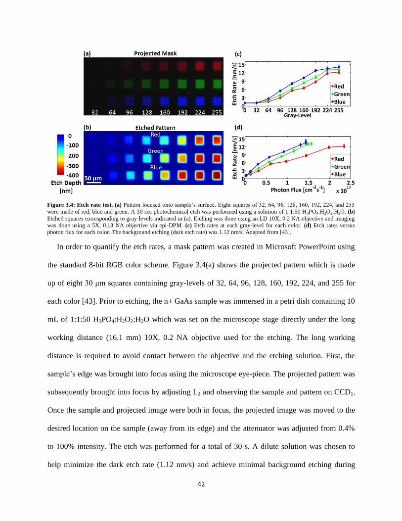
42
In order to quantify the etch rates, a mask pattern was created in Microsoft PowerPoint using
the standard 8-bit RGB color scheme. Figure 3.4(a) shows the projected pattern which is made
up of eight 30 μm squares containing gray-levels of 32, 64, 96, 128, 160, 192, 224, and 255 for
each color [43]. Prior to etching, the n+ GaAs sample was immersed in a petri dish containing 10
mL of 1:1:50 H3PO4:H2O2:H2O which was set on the microscope stage directly under the long
working distance (16.1 mm) 10X, 0.2 NA objective used for the etching. The long working
distance is required to avoid contact between the objective and the etching solution. First, the
sample’s edge was brought into focus using the microscope eye-piece. The projected pattern was
subsequently brought into focus by adjusting L2 and observing the sample and pattern on CCD1.
Once the sample and projected image were both in focus, the projected image was moved to the
desired location on the sample (away from its edge) and the attenuator was adjusted from 0.4%
to 100% intensity. The etch was performed for a total of 30 s. A dilute solution was chosen to
help minimize the dark etch rate (1.12 nm/s) and achieve minimal background etching during
Figure 3.4: Etch rate test. (a) Pattern focused onto sample’s surface. Eight squares of 32, 64, 96, 128, 160, 192, 224, and 255
were made of red, blue and green. A 30 sec photochemical etch was performed using a solution of 1:1:50 H3PO4:H2O2:H2O. (b)
Etched squares corresponding to gray-levels indicated in (a). Etching was done using an LD 10X, 0.2 NA objective and imaging
was done using a 5X, 0.13 NA objective via epi-DPM. (c) Etch rates at each gray-level for each color. (d) Etch rates versus
photon flux for each color. The background etching (dark etch rate) was 1.12 nm/s. Adapted from [43].

43
alignment. After the 30 seconds, the sample was cleaned using a standard degreasing procedure,
placed back in the microscope, and imaged using epi-DPM with a 5X, 0.13 NA objective.
The resulting etch is shown in Fig. 3.4(b) [43]. The mean and standard deviation of the etch
depth was measured for each square and used to compute the differential etch rates. The
measured background (dark) etch rate was then added to the differential etch rate to obtain the
absolute etch rate. Figure 3.4(c) plots the absolute etch rate vs. gray-level for each of the three
colors. A slight increase in roughness was observed at higher intensities as indicated by the
longer error bars, which depict the standard deviation. The known etch rates were then used to
choose the etch times and gray-levels required for a desired feature height in all subsequent
etches [43].
To provide etch rates independent of our particular setup, we measured the power of the
incident light using the Newport Optical Power Meter 1918-C and divided the irradiance by the
energy per photon to compute the photon flux. The etch rate versus photon flux is shown in Fig.
3.4(d) [43]. A separation in the etch rates for the different colors is apparent. The bandgap of
GaAs is Eg = 1.43 eV, where the cutoff wavelength for absorption is λmax = 868 nm. The
absorption coefficient for GaAs at 633 nm, 532 nm, and 488 nm is 3.93 x 104 cm
-1, 7.94 x 10
4
cm-1,
1.24 x 105 cm
-1 respectively and the skin depth for these wavelengths is 255 nm, 126 nm,
81 nm [43]. On a per photon basis, the shorter wavelength light generates carriers closer to the
surface, which results in faster etch rates. When using H3PO4:H2O2:H2O to etch n+ GaAs, the
hydrogen peroxide initiates the reaction by oxidizing the GaAs. The phosphoric acid can then
come in and remove the resulting oxide. Deionized water, of course, acts as the diluent which
helps minimize the unwanted dark etching. The exact ratio of constituents has a marked effect on
the etch rates, whether the solution is diffusion or reaction limited, as well as the surface

44
roughness. At low gray-levels, the etching process is reaction-limited, where minority carriers
(holes) are required for the oxidation process. At higher gray-levels, the etch rate begins to
saturate and the process becomes diffusion-limited, where the local reagents are being consumed
faster than new species can diffuse back into the surface regions. To achieve the highest quality
results, gray-levels were kept below 200 for subsequent etches, avoiding saturation effects.
The next step in the characterization process was to determine the etch feature resolution
using our new digital projection photochemical etching system. Mask patterns containing
selected portions of the USAF-1951 target were created for each color with feature sizes ranging
from 16 µm down to 1.2 µm [89]. The targets were made up of rectangles of various widths,
with some at 2.38 μm, 2 μm and 1.68 μm, near our resolution limit. All colors produced
resolvable strucutres at 2.38 and 2 μm, but not at 1.68 μm. Results from the green mask were
chosen to represent our typical etch feature resolution. The mask in Fig. 3.5(a) used a grey-level
of 96 for the green background and the 0 for the rectangular features. Low gray-levels were
selected to minimize roughness. This mask configuration results in a differential etch rate of 2.75
nm/s. A 36 second etch was then performed following the procedure described above. A 5X,
0.13 NA objective, resulting in a 250 x 335 μm2 field of view, was used to capture an image of
the entire etched pattern as shown in Fig. 3.5(b) [43]. Here the resolution is limited by the
imaging optics and the true etch feature resolution is not apparent. A zoomed-in image was then
taken from the dotted rectangle shown in the top-left corner of Fig. 3.5(b) using a 20X, 0.8 NA
objective (800 nm resolution). Using green light, the 2 μm features are clearly resolved and three
peaks at 1.4 μm are also faintly visible. The etch feature resolution can be improved using a
higher NA objective, given that the objective does not come in contact with the etchant when the
sample is in focus. The etch feature resolution is comprised of three components: (1) the

45
diffraction limit of the light used in etching, (2) the diffusion of carriers due to the induced
photochemical etching process (about 1.1 µm for n+ GaAs at room temperature [43]), and (3)
aberrations and imperfections in the optical system. The optical resolution limit for red, green,
and blue light using the 10X, 0.2 LD objective is 1.9, 1.6, and 1.4 μm respectively, according to
Abbe’s formula. Additional broadening is due to the diffusion of carriers and imperfections in
the optical setup. Slight discrepancies between the vertical and horizontal resolution are also
present due to the rectangular geometry of the projector’s RGB subpixel configuration.
3.2.3 Experimental Results
Figure 3.6 shows the measured topography of various test structures fabricated using our digital
projection photochemical etching technique [90]. Figure 3.6(a) contains the projected pattern
used to fabricate a multi-level structure in a single etching step. The pattern contains grey-levels
Figure 3.5: Resolution Test. (a) Projector pattern (selected portions of the USAF-1951 target) focused onto the sample’s
surface. (b) Etched sample imaged with 5X, 0.13 NA objective (2.5 μm lateral resolution). (c) Image from lines in series 1
captured using a 20X, NA = 0.8 objective (800 nm lateral resolution). Based on this test, the etch feature resolution using our
photochemical etching setup is at least 2 μm, worst case. Adapted from [43].

46
of 0, 60, and 78 which were calibrated to have widths of 150 and 75 µm and to produce heights
of 0, 50, and 100 nm using a single 33 s etch. The gray-levels and etch time were selected based
on the etch rates computed in Fig. 3.4(c). Figure 3.6(b) then reveals the topography of etched
structure. Figure 3.6(c) shows the histogram of the structure and the mean heights of 0, 50.7, and
101.6 nm for each of the three layers illustrating the high degree of process control and
repeatability. Figure 3.6(d) shows the epi-DPM height map of our standard control sample, a
Figure 3.6: Test structures. (a) Image from digital projector focused onto the sample’s surface and used to define the etching
pattern. The projected image used grey-levels of 0, 60, and 78 and a single photochemical etch was performed for 33 seconds.
The mask geometry, gray-levels, and etch time were calibrated to produce a multi-level structure with widths of 150 µm and 75
µm and heights of 0, 50 and 100 nm. (b) DPM height map of stacked cubes. (c) Histogram of image in (b) showing mean heights
of 0, 50.7, and 101.6 nm for the three levels. (d) DPM height map of a PC etched micropillar. A mask pattern with grey-levels of
0 and 136 was used for the pillar and background respectively. PC etching was performed for 60 seconds resulting in a mean
height of 304.9 nm. It was calibrated to have a 100 μm diameter and a height of 300 nm. (e) Cross-section of pillar in (d) showing
the dimensions and edge resolution. (f) Topographical profile of PC etched Archimedean spiral: a complicated grayscale
structure with a peak height of 100 nm and a width of 30 µm, which was fabricated in a single 33 second etch. Adapted from
[43].

47
micropillar, which was fabricated in a single 60 second etch. Since light itself is used to define
the structure, there is no need for spin coating photoresist, aligning, exposing, or developing in
the cleanroom, which significantly reduced the time required to fabricate new control structures
for imaging. A projected image using blue light with grey-levels of 0 and 136 for the pillar and
background respectively was used and etching was performed for 60 seconds It was calibrated to
have a 100 μm diameter and a height of 300 nm. Figure 3.6(e) shows a cross-section of the pillar
in (d) showing meaured diameter and height to be 99.4 μm and 304.9 nm. A typical wet etch,
which is isotropic, results in 1 nm of undercutting per 1 nm of etching, resulting in an edge
resolution of ε = Δx/Δy = -1. Using our current method, we instead see a broadening effect due
to the carrier diffusion which results in an edge resolution of ε = Δx/Δy = 30. This broadening
effect is currently the main bottleneck of this budding technique, but may be somewhat improved
by pre-warping the projected pattern in order to achieve more vertical sidewalls or by PSF
engineering. To illustrate our ability to produce continuously grayscaled structures, an
Archimedean spiral was fabricated using a continuous grayscale mask pattern created in
MATLAB. The gray-levels increased linearly around the spiral from 0 at the center to 96 at the
outer region. The width was calibrated to be 30 μm with a maximum height of 100 nm. Figure
3.6(f) shows the surface topography of an etched spiral taken using epi-DPM. It is not practical
to fabricate such a structure using conventional photolithography, as it would need to be broken
up into many discrete steps, each requiring its own series of processing steps. Using our
technique, this structure was etched in 33 seconds. The standard deviations for each of the flat
regions of the multi-level cubes and micropillar reported in Figs. 3.6(b) and 3.6(d) were recorded
in order to quantify the roughness of our fabricated structures. These values indicate that the

48
roughness is comparable to the that of a standard wet etch under typical cleanroom conditions [2,
15, 43].
Using our ability to create grayscale structures with ease, we fabricated a series of microlens
arrays. Figures 3.7(a) and (b) show a selected portion of the mask and the resulting etch for one
of the microlenses [43]. Figure 3.7(c) then shows a comparison between the projected mask
pattern and horizontal and vertical slices taken from (b). In the regions of the mask in (a) which
are darkest, the surface will etch slowest, forming the top of the lens. In the lighter regions, it
will etch faster, forming the base of the lens. This is why the mask pattern appears inverted. The
comparison between the two slices helps to illustrate the symmetry of the etch. Finally, Fig.
3.7(d) shows a 3D reconstruction of a 2 x 2 portion of the array, which was calibrated to have
heights of 500 nm, 100 µm diameters, and a 120 µm pitch [15, 42]. The measured heights over
Figure 3.7: Digital projection photochemical etching of microlens arrays. (a) Grayscale mask projected onto sample plane.
(b) epi-DPM height map of etched microlens. (c) Projector intensity profile and comparison of horizontal and vertical cuts taken
from (b) illustrating symmetry. (d) Microlens array displaying height, lens diameter, and pitch, which were calibrated to be 500
nm, 100 μm, and 120 μm respectively. Adapted from [42].

49
the entire array, ranged from 425-590 nm. The pitch and diameter had only small variation
ranging from 95-105 µm and 120-125 µm respectively.
3.2.4 Conclusions
Digital projection photochemical etching is capable of fabricating grayscale and multi-level
structures in a single processing step, a feat not possible using conventional photolithography.
The etch rates for a given material/etchant combination can be determined by performing the
etch rate test described above [2, 15, 42]. The worst-case etch feature resolution, as determined
by etching selected portions of the USAF-1951 resolution target, is 2 µm. The edge resolution is
an order of magnitude worse than that of standard isotropic wet etching and proves to be the
major bottleneck of this technique in its current state. The roughness of etched features was also
characterized and is comparable to what is obtained using standard wet etching. By combining
the PC etching and DPM setups, dimensions of the fabricated structures can be measured in-situ
in a completely non-destructive manner, which This is not possible with scanning electron
microscopy (SEM), transmission electron microscopy (TEM), atomic force microscopy (AFM),
or other similar inspection methods [43].
3.3 Dissolution of Biodegradable Electronics
3.3.1 Introduction
Similar to the way that dissolvable sutures disintegrate over time without requiring additional
surgery for removal, electronic components have been proposed using specific materials that
could be implanted into the body and dissolve over time without producing harmful byproducts.
Devices using these materials have been shown to sustain adequate performance until their
function is complete, then rapidly degrade and resorb into the body [42, 91, 92].

50
Previously, biodegradable electronic circuits were developed using either water soluble
organic constituents [93] or non-transient electronic materials on bioresorbable substrates [94,
95]. Recently, a new set of materials has been proposed which includes Si as a semiconductor
material, Mg for conductors, MgO or SiO2 as dielectrics, and silk for the substrate [93, 96]. All
of these materials are water-soluble and do not produce any harmful byproducts during the
dissolution process. Moreover, Si-based electronics have exhibited much better performance in
comparison to their organic counterparts.
3.3.2 Experimental Results
The dissolution process of Si in both bovine serum and phosphate buffered saline (PBS) was
monitored using laser DPM in transmission mode in order to obtain quantitative height
measurements throughout the process and compute the dissolution rates [93]. Samples for this
study were prepared using silicon-on insulator (SOI) wafers, which are comprised of a top Si
layer, a buried oxide layer (SiO2), and a Si substrate. The fabrication was done by first creating a
periodic array of tiny through holes on the top Si layer, which allowed hydrofluoric acid (HF) to
reach and remove the underlying buried oxide (SiO2) in the subsequent etch. The detached Si
layer was then transfer printed upon an SiO2 substrate using a spin cast film of SU-8 as the glue
layer. The Si layer was then etched using standard photolithography down to the glue layer,
forming the “UIUC” initials, which were 100 nm in height, the initial height of the top Si layer.
The width of the lines forming the letters was 15 μm and each letter was 75 μm long (top to
bottom). The two sets of samples were placed into bovine serum and PBS solutions and stored in
an incubator at body temperature (37 °C) [2, 44]. The dissolution rate is faster at higher
temperatures as well as at higher pH levels. The samples were removed every 8 hrs for imaging.
After imaging was complete, they were placed in a fresh solution in a clean container and stored

51
back in the incubator, which helps avoid contamination which has proven to have a mild effect
on the dissolution process [44].
Figures 3.8(a-d) show DPM images of the “UIUC” initials at four different stages during
dissolution [2]. The initial height map (t = 0 hrs) was compared to values obtained using the
Alpha Step IQ Profilometer, which both gave mean heights of 97 nm. Images were then taken at
8 hr intervals. Figure 3.8(e) shows the cross-sections from the images in (a-d) [2, 44]. The cross-
sections were taken vertically along the “I” in “UIUC”. The heights at 0, 8, 16, and 24 hours
were 97 ± 2.1 nm, 67 ± 2.9 nm, 31 ± 1.9 nm, and 0 ± 0.7 nm respectively. The dissolution rate is
not perfectly linear, but is highly repeatable under comparable conditions. Figure 3.9 is similar to
Figure 3.8: Dissolution of biodegradable electronic materials. Dissolution of Si in serum at 37 °C. (a-d) 3D topographic
profiles of Si during dissolution at 0, 8, 16, and 24 hrs. (e) Corresponding cross-sectional profiles showing heights at various
times in the dissolution process. Measured heights are 97 nm (0 hrs), 67 nm (8 hrs), 31 nm (16 hrs) and 0.0 nm (24 hrs). The
dissolution process is not perfectly linear. The 97 nm layer completely dissolves within 24 hrs. Adapted from [2, 44].

52
Fig. 3.8, but shows the dissolution of Si in PBS rather than serum [2, 44]. Here, the measured
heights at 0, 8, 16, and 24 hours were 97 ± 2.6 nm, 62 ± 3.4 nm, 29 ± 6.1 nm, and 0 ± 1.5 nm
respectively.
3.3.3 Conclusions
Despite a small degree of non-linearity and non-uniformities during the process, we were able to
successfully determine the dissolution rates of Si in both PBS and serum. The dissolution of
other materials in a variety of media is currently being studied for use in dissolvable electronics
applications. The final goal is to capture the resorption of a complete electronic device in its
entirety.
Figure 3.9: Dissolution of biodegradable electronic materials. Dissolution of Si in Phosphate Buffered Saline (PBS) at 37
°C. (a-d) 3D topographic profiles of Si during dissolution at 0, 8, 16, and 24 hrs. (e) Corresponding cross-sectional profiles
showing heights at various times in the dissolution process. Measured heights are 97 nm (0 hrs), 62nm (8 hrs), 29 nm (16 hrs) and
0 nm (24 hrs). The dissolution process is not perfectly linear. The 97 nm layer completely dissolves within 24 hrs. Adapted from
[2, 44].

53
3.4 Expansion and Deformation of Materials
3.4.1 Introduction
Before hydrogen fuel cell technology can become a practical source of energy in the everyday
sense, safe and reliable sensors must be developed capable of detecting H2 well below the lower
explosive limit (LEL) of 4% in air [44]. Many sensors have been developed for this purpose
which rely on the properties of palladium (Pd), an element known to react readily with H2 gas
and produce electrical, optical, and structural changes which provide several options for
detection [97]. Some of these sensors include functionalized waveguides or laser structures [98],
optical fiber sensors [99, 100], plasmonic devices [101-105], and transmission/reflection
monitoring of thin films [104]. While the electrical and optical changes are easy to measure and
are well documented in the literature, much less is known about the minute structural changes
that occur. In this work, we investigate the hydrogen induced axial expansion of Pd microdisks
in order to better characterize the nanoscale structural changes which can be either incorporated
into existing simulations or used to simulate entirely new sensors [106, 107]. There exists an
abundance of studies on the PdH system for bulk materials [2, 97], and more recently on
nanoparticles [108, 109], but few studies have been done on micro and nanoscale structures,
which are more often used in modern sensor applications.
3.4.2 Physical Mechanism
When gaseous H2 molecules interact with Pd, they separate into single atoms, breach the surface,
and diffuse into the face-centered cubic (FCC) lattice [110]. The hydrogen atoms then bond to
interstitial sites between the Pd atoms forming PdH. Initially, at low concentrations, the
palladium-hydrogen system is said to be in the α-phase. At this point, the process is completely
reversible, meaning that if H2 gas is removed from the ambient, the hydrogen will diffuse out
from the lattice allowing the Pd structure to return to its original shape. This property is essential

54
if sensors are to be reusable. As the H2 concentration is increased, the lower critical limit αmax is
reached. Beyond this point, regions containing PdH swell producing β regions. Since the two
phases are immiscible at standard temperature and pressure, the palladium-hydrogen system is
said to be in the α + β phase [97]. As the H2 concentration is increased further, it will eventually
reach the upper critical limit βmin, where only β regions remain. Values for αmax and βmin can vary
drastically depending on the film thickness as well as the deposition method and angle. The
formation of β regions within the Pd lattice is referred to as hydrogen induced lattice expansion
(HILE), where up to 3.5% lattice expansion has been reported Due to the symmetry of the Pd
lattice and available bonding sites, the induced expansion is known to be isotropic in nature
[109]. However, when the Pd is not well-adhered to the substrate, which is often the case with
quartz, the expansion can lead to buckling, and micro-blistering or micro-cracking of the Pd film
[109].
It turns out that such effects, at least at low concentrations and exposure times, are also
reversible [101, 102]. With concentrations >> βmin, plastic deformations can form resulting in
permanent structural changes in the Pd. With our films, symptoms of permanent deformation
have been recorded for concentrations at or above 1.5% H2. Through many repeated
experiments, we have found that a single high concentration exposure or many repeated
exposures even at moderate concentrations may lead to irreversible structural changes [101,
102]. For this reason, we typically attempt to detect hydrogen at very low concentrations, at least
an order of magnitude below the lower explosive limit of 4% in air. In general, response times,
recovery times, and overall sensitivity of a Pd sensor based on structural changes depend heavily
on many factors including quality of film adhesion, film thickness and method of deposition,
substrate material, and also the particular geometry of the sensor [109, 111].

55
Introduction of hydrogen into the Pd lattice causes changes in both the carrier concentration
and mobility, which alters the conductance and is easily detected electrically [97]. The H atoms
bonded to the interstitial sites also serve as electron donors, which provide a means of detection
via optical sensors [112]. In this case, orbital hybridization of the electrons with the 4d band of
the Pd atoms changes the Fermi level, which alters the optical transition rate, resulting in
changes in both the real and imaginary parts of the refractive index [98, 100-102, 104, 107, 109].
Hydrogen detection can also be based on structural changes in the Pd, which are much more
difficult to measure than the electrical and optical changes mentioned previously [106, 109]. For
this reason, hydrogen induced lattice expansion of thin films or microstructures is not well
documented in the literature. The small nanoscale changes in the lattice that occur during
hydrogen exposure are difficult to measure using conventional techniques. However, recent
advances in quantitative phase imaging (QPI) have led to new imaging systems capable of
capturing nanoscale dynamics in a wide variety of environmental conditions [97]. Epi-
illumination diffraction phase microscopy (epi-DPM) is a reflection–based QPI technique with
sub-nanometer height measurement accuracy and has been used successfully to monitor
semiconductor wet etching [26, 41], photochemical etching [42], microdroplet evaporation [42,
72], and material deformation [113], as well as to detect in-line killer defects in semiconductor
wafers [114].
3.4.3 Experimental Setup and Sample Preperation
Figure 3.10 shows a schematic of the experimental setup used for this study [45]. Multiple mass
flow controllers and regulators were added to the setup and used to control the gas flow and
pressure of the hydrogen and nitrogen gasses via LabVIEW. Two valves were also employed to
pre-charge the lines and prevent any added delay in H2:N2 pulse shape due to diffusion of the gas

56
through the lines. This particular epi-DPM setup provides topographic height information with
0.55 nm spatial (i.e., point to point) and 0.43 nm temporal (frame to frame) sensitivity [97].
Furthermore, averaging over a region within the image, or over a series of frames, can further
reduce the spatial and temporal noise. In fact, both averaging schemes are employed when
processing the axial expansion data from the Pd microdisks [42, 72].
In order to house the samples, we custom-made an aluminum flow chamber with a transparent
viewing window, which was set at a small angle (~7°) to avoid multiple reflections which would
result in additional unwanted fringes [97]. The flow cell was 32 mm x 19 mm at the base and 5
mm in height. The slanted viewing window added an additional 4 mm of height at one end
resulting in a total volume of 4.25 x 103 mm
3 [97]. The samples were fabricated using e-beam
evaporation through a shadow mask to form Pd microdisks on a quartz (SiO2) substrate. SiO2
Figure 3.10: Experimental setup for epi-DPM imaging system with gas flow. epi-DPM was used to monitor the hydrogen
induced axial expansion of the palladium microdisks in-situ. A stainless steel chamber with a transparent window was custom-
built to house the samples. Mass flow controllers and regulators controlled the pressure and gas flow of hydrogen and nitrogen
via LabVIEW. Abbreviations: SMF, single-mode fiber; FC, fiber collimator; CL, collector lens; OBJ, objective; TL, tube lens;
L1/L2, lenses; V1/V2, valves; MFC, mass flow controller; REG, regulator, VAC, vacuum line. Adapted from [46].

57
was selected due to its extensive use and importance in fiber-based H2 sensing applications [97].
The shadow mask approach was used since poor adhesion between Pd and the quartz substrate
prohibited the use of standard lift-off techniques via conventional lithography. The shadow mask
was placed in close proximity to the sample and was comprised of an array of 180 µm diameter
holes with a 350 µm pitch. Figure 3.11(a) shows a cross-sectional view of the microdisk sample.
First, a 260 nm Pd layer was deposited. Then, the shadow mask was removed and a 40 nm
blanket deposition of Pd was performed [104, 115]. This ensures that both the microdisks and the
background have the same complex refractive index, which allows us to decouple any changes in
the height from changes in the complex refractive index during exposure. Variable angle
spectroscopic ellipsometry (VASE) data yielded a complex refractive index of 1.56 + 3.64j for
our Pd structures. To allow us to verify the thicknesses of the blanket layer, the blanket
deposition was also masked with a straight edge of Kapton tape, which can be seen in Fig.
3.11(b) [97]. Here, the dark region is quartz where the light does not reflect well. The bright
regions contain the deposited Pd.
Figure 3.12(a) shows the epi-DPM height map of the Pd microdisk along with its initial
dimensions prior to hydrogen exposure [97]. The initial height relative to the background was
Figure 3.11: Fabrications of Pd microdisk sample. (a) Cross-section of the sample showing the 260 nm tall Pd microdisks on
a quartz substrate with the 40 nm blanket deposition. (b) Bright field image of the sample showing regions with and without the
blanket deposition. Adapted from [46].

58
recorded as 264.4 nm with a full width at half maximum of 181.1 μm. The mean height of the
microdisk was measured by averaging over a circular region within the top portion of the
microdisk where the surface was flat. A calibration run using only N2 was then performed and
the standard deviation of the height was recorded in order to characterize the temporal stability
of our measurement system. Figure 3.12(b) reveals that the temporal noise in the height
measurement during 300 standard cubic centimeters per minute (sccm) of N2 flow was 0.16 nm.
3.4.4 Experimental Results
Figure 3.13(a) shows the change in microdisk height induced by a 0.4% H2 pulse over the 300
min duration [97]. An initial 30 min calibration run was performed with pure N2 at 300 sccm.
The H2 was then turned on and the flow rates were adjusted to maintain 300 sccm. A 90 min H2
pulse was started and shut off at the 120 min mark. The chamber was then purged with pure N2
at 300 sccm for 3 hours. Images were captured every 6 s during pure N2 exposure and at 3 s
intervals throughout the H2 pulse. A slight drift of the sample accrued during exposure, only a
fraction of a CCD pixel, roughly 100 nm in the sample plane. In order to remove this drift and
obtain accurate results, sub-pixel image registration was performed. This was done by first cross-
correlating each frame during the 30 min N2 baseline with the initial frame, fitting the results
with a second order polynomial in the neighborhood of the maxima in order to locate the position
Figure 3.12: Initial measurements. (a) Height map of a palladium microdisk obtained via epi-DPM; initial
dimensions before hydrogen exposure are displayed. (b) Stability of height measurement during N2 baseline run.
Adapted from [46].

59
of this maxima, rmax with sub-pixel precision, and then linearly interpolating the height map onto
a grid shifted by -rmax [97]. After registration was complete, these baseline images were averaged
to reduce noise, resulting in a baseline image that could be used to compute the instantaneous
height change in the most accurate manner. Next, every image throughout the pulse test was
registered with the baseline image and the instantaneous height change images were computed
via subtraction. To further reduce the temporal noise floor, the images were then averaged for 1
min, which corresponds to 10 frames during the N2 exposures and 20 over the duration of the H2
pulse. Using this approach, we were able to accurately measure the axial expansion of the
microdisk in a spatially and temporally resolved manner [97].
Figure 3.13(b) shows the instantaneous height change images of the microdisk during the
expansion along with their corresponding histograms [97]. The frames were selected from Fig.
Fig. 3.13: Differential height measurements during hydrogen exposure. (a) Measured average height change of the Pd
microdisk during 0.4% pulse test. (b) Selected frames indicated in (a) showing the local height change at various times. With
hydrogen exposure, the histogram splits into two peaks showing how the height of the microdisk increases. After the hydrogen is
turned off, the peaks then merge back together and the microdisk height nearly returns to its baseline value. (c) Instantaneous
expansion rate before exposure, during expansion, during recovery, and after recovery. All scale bars are 100 µm. Adapted from
[46].

60
3.13(a) in order to sample the axial expansion process evenly. The expansion process can be
clearly observed by scanning the images in chronological order. The initial histogram during the
N2 calibration run has a peak with zero height, which then splits into two peaks during H2
exposure, where one remains at a height of zero (the background) while the other indicates the
amount of expansion. The peaks subsequently merge back into a single one upon purging the
chamber with N2. Furthermore, small deformations, or local heterogeneities, can be observed
during parts of the expansion and recovery process. Although these are more easily identifiable
in the instantaneous height change images, they can also be observed in the histogram by
measuring the width of the peaks.
Figure 3.13(c) contains a subset of the spatially and temporally resolved instantaneous rate of
axial expansion at four select moments during the experiment: (1) during the calibration run (6
min), (2) during expansion (36 min), (3) during recovery (126 min), and (4) near the end of the
N2 purge (295 min) [97]. These images were computed pixel by pixel using a linear regression of
the height change as a function of time during a 10 min window centered at the times specified in
Fig. 3.13(c). Here, we see that the expansion rates before exposure and near the end of the purge
are negligible. The axial expansion and contraction rate during exposure and at the beginning of
recovery are about 0.1 nm/min. The expansion and contraction rates also appear to be relatively
uniform over the Pd microdisk.
Similar pulse tests were repeated for several other H2 concentrations in order to quantify the
dependence of axial expansion on the hydrogen concentration. Figure 3.14(a) shows the height
changes in nm for the series of pulse tests [97]. The response times for this particular sample
were all approximately 30 min in duration. Following the N2 purge, the microdisk’s height

61
returned to its initial value, at least to within the noise floor of the system. The recorded recovery
time was approximately 2-3 hours for each case [97].
Figure 3.14(b) shows the percent change in height, Δh, as a function of the H2 concentration
in percent, c, for each pulse test [97]. The axial expansion process, for ideal films at constant
temperature, is limited by surface adsorption, a process governed by the Langmuir or Freundlich
isotherms depending on the concentration [97]. It turn out that the Freundlich fit is more
appropriate given the low adsorbate concentrations used in this study. This power law fit works
well, assuming that the axial expansion is linear with concentration [116]. Fitting the data to a
power law provides a model for the change in microdisk height Δh(c) = kcn
and gives k = 1.28 ±
0.06 and n = 0.51 ± 0.04 [117]. These results agree well with Sievert’s law (n = 0.5) and the
anticipated square root dependence for diatomic gases [97].
3.4.5 Conclusions
In conclusion, we have shown that epi-DPM can be used to monitor the nanoscale axial
expansion of Pd microdisks during H2 exposure. The measured temporal noise floor for the
height measurements during gas flow was 0.16 nm. Using our technique, we were able to
determine the axial expansion coefficient as a function of H2 concentration, which agreed well
Sievert’s Law. Moreover, the low noise floor, averaging schemes, and linear regression allowed
Figure 3.14: Hydrogen induced height changes of palladium. (a) Measured height change due to hydrogen exposure. (b)
Percent change in height with Freundlich fit: Δh(c) = kcn, where k = 1.28 ± 0.06 and n = 0.51 ± 0.04 and Δh and c are in percent.
Adapted from [46].

62
us to quantify the axial expansion rate very accurately in a spatially and temporally resolved
manner. We anticipate that these reported measurement capabilities will lead to the development
of new classes of sensors based on nanoscale structural changes for use in a wide variety of
fields.
3.5 Surface Wetting and Evaporation
3.5.1 Introduction
The dynamics of surface wetting and evaporation are subjects of extensive study in the fields of
physics, chemistry, and engineering. Applications of particular interest include microfluidics,
mechanical lubrication [117], water-resistant and self-cleaning surfaces [118], spray cooling
[119, 120], microlens fabrication [121], thin-film deposition [122-124], self-assembly of
nanoparticles [124-127], biochemical assays [128-130], deposition of DNA/RNA micro-arrays
[131], manufacture of novel optical and electronic materials [132, 133], inkjet-printing
technology [134] and printable electronics [134-137]. Knowing the surface wetting properties of
particular liquid/substrate combinations is of great interest in developing effective high-yield
industrial processes [93, 134-136, 138-140].
There are few methods available for the characterization of surface wetting and evaporation.
Among these, the sessile drop or goniometric method [46] is widely used. This technique uses a
syringe to place a single, isolated droplet of a predetermined volume onto the substrate. The
syringe is oriented perpendicular to the substrate and can be used to measure the receding and
advancing contact angles by siphoning or depositing more liquid. Once the droplet is in place, a
high-resolution image of the droplet can be taken from the side. Image analysis software is then
used to compute the height, contact radius and contact angle. Though this method gives an
accurate measurement of the droplet height, it relies heavily on the spherical cap approximation

63
(SCA) to evaluate other droplet parameters. Further, the contact angle and drop radius are
obtained from a single viewing angle and assumed to be constant throughout the entire droplet,
which is not true for many cases. Also, this technique has difficulty with small contact angles (<
10°) and smaller (micron-sized) droplets in general.
Scanning white light interferometry has been employed to make profile measurements of the
droplet near the contact line [141, 142]. It records interference fringes while scanning over the
specimen, which is capable of producing a 3D profile of the droplet. As the vertical scanning is
time consuming, it is only suitable for very slowly evaporating droplets. An imaging technique
based on the measured reflectivity of the liquid film at each pixel location along the entire drop
profile has been used to measure the drop shape [143]. Using the gray value plots of the naturally
occurring interference fringes result from the reflection of light at the liquid-vapor and the solid-
liquid interfaces, thickness profiles for the drops are obtained. The curvature and the apparent
contact angle are then calculated simultaneously by best fitting the experimental thickness
profile. Further, laser light interference microscopy has been used to study the dynamics of liquid
drop spreading [144]. From the movie of the interferometer fringes, spreading speed at the drop
edge was measured and the edge profile was reconstructed. However, as these techniques
involve fitting and counting fringe numbers for thickness profile measurement, the fraction of
fringe will inevitably lead to error.
Here, we demonstrate a real-time quantitative phase imaging (QPI) method [145] capable of
capturing the dynamics of surface wetting including direct time-dependent measurements of the
volume, surface area, height, contact radius, radius of curvature, contact angles around the entire
droplet, and mass flux density [42]. QPI is an emerging technology that measures shifts in the
optical pathlength created by the sample at each point in the image, which allows for the

64
reconstruction of surface topography with nanoscale accuracy. This information has enabled new
studies in biomedicine over the past decade [46]. The quantitative phase images obtained using
this technique allow for the full 3D reconstruction of the droplet during evaporation.
3.5.2 Experimental Results
We used we used the DPM imaging system in transmission mode, in order to study evaporating
microdroplets on glass substrates with different surface treatments [26]. Because the refractive
index of water is known, the quantitative phase image captured by this approach allows us to
acquire a full 3D description of the evaporating droplet in real-time. A background image is first
taken from a portion of the substrate containing no droplets. This is used to subtract the
background noise from all subsequent images [46]. Droplets of distilled water are sprayed onto
the substrate using a standard spray bottle. Since we can directly measure the volume, there is no
need to pipette a droplet of predetermined volume onto the sample as in the sessile drop method.
Furthermore, we are not limited to the assumption that the droplet is spherical and can
characterize droplets of arbitrary shape. Once the sample is prepared, a time-lapse series is
recorded, which reveals the dynamics of the evaporation process. All time lapses were taken with
a 40 ms exposure time and a 200 ms acquisition period. A top-down view of the topographical
height map obtained via DPM is shown in Fig. 3.15(a) [42, 72]. Figure 3.15(b) illustrates how
we can directly measure the height, contact radius and contact angle from any arbitrary cross-
section of the droplet. Figure 3.5(c) shows a zoomed-in view of the contact angle measurement
which can be obtained using a tangent fit [46]. From this data we are able to directly measure
many of the important parameters required to assess the wettability of a given liquid/substrate
combination [146].

65
To further characterize the evaporation process we took the gradient of the image and
computed the gradient angles throughout the droplet. The gradient angle at the droplet’s edge
gives the contact angle. By thresholding and binary masking the image based on both height and
angle information, we were able to pick out the edge of the droplet. Figure 3.15(d) shows a map
of contact angles [46]. The resulting histogram shown in the inset reveals the mean, median,
mode and standard deviation of the contact angles around the entire droplet. There is an
abundance of statistical information acquired with this technique. Moreover, the volume, surface
area, height, contact radius, radius of curvature, contact angles, and mass flux density can be
determined via direct measurements at different moments in time during evaporation.
To further verify the accuracy of our system, for small contact angles in particular, we imaged
a microlens array (MLA150-7AR from Thorlabs), which has a contact angle specification of
Figure 3.15: Direct measurements of a water droplet during evaporation. (a) DPM height profile. (b) Cross-sectional profile
taken along the dotted-line in (a). Height, contact radius, and contact angle can be measured directly from the quantitative phase
image. (c) Zoomed-in portion of profile taken along solid line in (a). Contact angles can be measured directly at any point around
the droplet’s edge. (d) Masked gradient angular profile displaying all contact angles. The inset in (d) contains the histogram
which readily gives the mean, mode, standard deviation and many other statistics about the contact angles around the entire
droplet. Adapted from [140].

66
1.37°. Our measurements revealed a contact angle of 1.58° with a standard deviation of 0.61°
averaged over all of the microlenses within the field of view (Fig. 3.16) [46].
It is well documented that evaporation occurs in three distinct phases [46]. In the initial stage,
known as the constant contact area mode, the contact line is pinned and the contact angle
decreases linearly with time. Within this regime, radial convection occurs in order to compensate
for the uneven evaporation along the surface of the droplet. As the droplet reaches the receding
angle, it can no longer produce the required radial flow in order to maintain equilibrium given its
diminishing volume. This results in depinning of the droplet boundaries and the second phase,
referred to as the constant contact angle mode. The contact angles remain nearly constant within
this regime, evaporation flux density is nearly uniform, and radial convection is minimal [147-
150]. Finally, as the evaporating droplet becomes very small, imperfections in the substrate take
over and the droplet enters a mixed mode, referred to as the drying mode, where both the contact
radius and angle recede rapidly. It is believed that for a perfectly flat substrate, stage 2 (constant
contact angle) will persist until complete evaporation has taken place.
Figure 3.17(a) (pinned-unpinned transition) shows selected frames from a time lapse taken of
an evaporating water droplet sprayedon a treated glass substrate [147-149]. The substrate was
Figure 3.16: Microlens verification. (a) DPM height profile of the microlens array (Thorlabs MLA150-7AR). (b) Masked
gradient angular profile showing contact angles around the perimeter of the microlens. The measured contact angle agrees well
with the 1.37° manufacturer specifications. Adapted from [140].

67
treated with ethanol and burned to achieve a more hydrophilic surface and encourage a smooth
transition between phases I and II. This sequence was taken using a 5X objective resulting in a
field of view of roughly 360 μm x 270 μm. The initial volume, height, and contact radius of the
droplet were 2.50 x 105 μm
3, 8.87 μm and 132 μm, respectively. The droplet is initially in the
pinned state and remains in this regime until the receding angle of 1.28° is reached after 5.2 s of
evaporation.
Figure 3.17: Pinned-unpinned transition. (a) Topographic height image and (b) corresponding angle map of evaporating water
droplet on ethanol-treated glass substrate. The evaporating droplet undergoes a clear transition between the constant contact area
mode and constant contact angle mode. This sample was prepared by treating the glass slide with ethanol and burning. Contact
angles decrease in a linear fashion until the receding angle is reached and depinning occurs around 5.2 s. This sequence was
taken using a 5X objective resulting in a 360 μm x 270 μm field of view. (c) Comparison between experimentally measured
volume and volume computed using the spherical cap approximation (SCA). (d-e) Time evolution of height and contact radius,
respectively. (f) Comparison of measured and SCA contact angle during evaporation. All SCA data was obtained by using the
measured values for height and contact radius. For figures (c-f), I indicates the constant contact area phase and II indicates the
constant contact angle regime. Adapted from [140].

68
The second row of images (Fig. 3.17(b)) are the corresponding gradient angle maps [46] .
These were created by taking the gradient of the image and computing the angle between the
gradient vector and the x-y plane. This gives the contact angles at the droplet’s edge. This
sequence more clearly illustrates the linear decrease in contact angles while the droplet is pinned.
In frames 1-26 (0-5.2 s), the contact angle decreases linearly with time, which can be observed as
the colors at the droplet edge change at a constant rate. After depinning occurs (frame 27
onward), the contact angle barely changes and the colors at the edge of the droplet remain nearly
constant. Further, the contact radius starts to decrease in a linear manner. This is indicative of
the second phase of evaporation i.e. constant contact angle mode [46]. The dynamic
measurements for volume (v), height (h), contact radius (a) and contact angle (ϴ) are presented
in Fig. 3.17(c-f), respectively [147-149]. In the pinned regime, the volume, height, and contact
angle all decrease at a nearly constant rate. This is a result of the pinned boundary conditions and
the non-uniform evaporation flux density [46]. The contact radius versus time plotted in Fig.
3.17(e) clearly indicates the transition from phases I to II where depinning occurs [148, 149].
The volume and contact angle are compared to the spherical cap approximation, where we use
height and contact radius data to compute these parameters. Although deviations in the volume
are minimal, the spherical cap approximation tends to over-estimate the contact angle, which is
an important parameter in determining the surface tension.
Figure 3.18(a) (partial pinning) shows selected frames from a time lapse sequence taken under
similar conditions except that an untreated glass cover slip was used as the substrate [46]. This
sequence was taken using a 10X objective resulting in a field of view of roughly 180 μm x 135
μm. Figure 3.18(b) shows the corresponding gradient angle maps [46]. The dynamic
measurements for volume (v), height (h), contact radius (a) and contact angle (ϴ) are presented

69
in Figs. 3.18(c-f), respectively using spherical cap approximation. The initial volume, height, and
contact radius of the droplet were 6.38 x 104 μm
3, 14.21 μm and 53 μm respectively. This
particular droplet exhibits partial-pinning in the lower-left corner, which is due to surface
roughness and chemical heterogeneity of the untreated sample [46]. The pinned contact line in
this region pulls the center of the droplet in this direction during evaporation. After 16.4 s of
evaporation, the droplet’s size becomes comparable to the microstructure of the substrate and its
imperfections. The droplet then enters the drying mode where the contact radius and angle
recede rapidly. This is also believed to be a result of an increase in the density of impurities
Figure 3.18: Partial pinning. (a) Topographic height image and (b) corresponding angle map of evaporating water droplet on an
untreated glass cover slip. The droplet exhibits partial pinning in the lower left-hand corner. Transition from constant contact
angle mode into the drying phase is observed after 16.4 s. This sequence a was taken using a 10X objective resulting in a 180 μm
x 135 μm field of view. (c) Comparison between experimentally measured volume and volume computed using the spherical cap
approximation (SCA). (d-e) Time evolution of height and contact radius, respectively. (f) Comparison of measured and SCA
contact angle during evaporation. All SCA data was obtained by using the measured values for height and contact radius. For
figures (c-f), II indicates the constant contact angle regime and III indicates the drying phase. Adapted from [140].

70
trapped within the droplet itself, forcing its behavior to deviate from the predicted theory. From
both of the gradient angle image sequences (more so from Fig. 3.18(b)), it can be observed that
the background where the droplet initially resided remains clean during evaporation. This
suggests that the droplet may be trapping impurities from the surface due to surface tension as it
moves inward. As in the treated glass case, the spherical cap approximation provides a good
estimate of the volume, but significantly overestimates the contact angle. It is noteworthy to
mention that instances of partial pinning are difficult to observe and impossible to characterize
when using the sessile drop or goniometric technique since these methods only produce a side
view.
3.5.3 Modeling
Several theoretical models have been developed in order to describe the evaporation of isolated
spherical droplets. In 1977, Picknett and Bexon [148] described the three modes of evaporation,
which are constant contact area (pinned), constant contact angle (depinned), and a mixed mode
(combination of pinned and unpinned). They developed isothermal diffusion theory models to
describe the evaporation in both the pinned and unpinned cases separately. The final regime,
referred to as the mixed or drying mode, is highly complicated and depends on several effects
which are difficult to model for the arbitrary case. In order to get their data to properly fit,
Picknett and Bexon introduced the f(θ) factor (θ is the contact angle), which they claim is
necessary to account for the presence of the substrate which hinders the evaporation process.
Simplifications to the f(θ) factor approach were made by Shanahan [149] and Rowan [148] in
subsequent years, but their approximations are only valid for larger contact angles. In 2012, a
more rigorous theoretical analysis was performed which resulted in a model valid for both

71
pinned and unpinned modes [151]. However, these models appear to work only for significantly
larger droplets where self-cooling and effects of the substrate can be deemed negligible.
For the pinned-unpinned case which begins in the constant contact area mode with the contact
radius constant, we used the spherical cap approximation to obtain the volume as a function of
the measured contact angle. We then used this result along with the Picknett and Bexon model
in order derive a model for the time evolution of the contact angle [152]. Figure 3.19(a) shows
the volume as a function of time and Fig. 3.19(b) shows the contact angle. A comparison is
made between our experimental data and the model we developed using equations from Picknett
and Bexon.
Figure 3.19: Evaporation models. (a) Time evolution of droplet volume for the pinned-unpinned case (from Fig. 3.17). A
comparison is made between the experimental data and the theoretical model. The volume decreases linearly during the constant
contact area mode (0-5.2 s). (b) Time evolution of the mean contact angle averaged around the entire droplet. A comparison is
made between the experimental data and the theoretical model. The contact angle also decreases linearly during the constant
contact area mode (0-5.2 s) and then levels out upon entering the constant contact angle mode (> 5.2 s). (c) Model fitting for the
partial pinning case (from Fig. 3.18). The volume2/3 is linear with respect to time during the constant contact angle mode (0-16.4
s). (d) Comparison of measured and modeled volume for the partial pinning case.

72
Under the spherical cap approximation, the volume (V), height (h), contact radius (a), and
contact angle (θ) are related as follows,
2 2(3 )
6
V h a h (3.1)
1tan
2
h (3.2)
Combining the two equations and taking the derivative with respect to time yields,
3 tan 3 tan
6 2 2
V a (3.3)
4
4sec
4 2
dV a d
dt dt
(3.4)
From the Picknett and Bexon model,
1/3
dVV K f
dt
(3.5)
2/3 1/3
0
1/3
4 3
sD c cK
(3.6)
where D is the diffusion coefficient of water vapor, cs is the saturated vapor concentration, c0 is
the vapor concentration of the ambient, and ρ is the density of water. The quantity (cs – c0)
drives the evaporation process. The empirical functions f(θ) and β(θ) are were taken from the
Picknett and Bexon model [46].
Combining Eqs. (3.3) through (3.5) yields,
d
gdt
(3.7)

73
2/3
2
62
3
a
(3.8)
1/3
4 1/3cos tan 3 tan2 2 2
g K f (3.9)
The contact angle as a function of time is then obtained by integrating Eq. (3.7).
For the partial pinning case which is initially in the constant contact angle regime, we fitted
the volume to the Picknett and Bexon model using the following equation where for constant
contact angle, K(θ) and f(θ) are constant,
2/32/3 2
3 iV V K f t
(3.10)
Figure 3.19(c) shows that the 2/3 power of the drop volume is linear and Fig. 3.19(d) shows
the volume as a function of time. A direct comparison is made between our experimental data
and the Picknett and Bexon model.
The f(θ) factor introduced by Picknett and Bexon is an empirical polynomial required to fit
the data. It was suggested that this factor is necessary to account for the effects of the substrate
which hinder the evaporation process. This empirical fit coefficient works well for large droplets
where effects from the substrate are less prominent. The droplets measured in our experiments
are 4 orders of magnitude smaller than in their experiments and the f(θ) factor determined for the
larger droplets is not applicable. Moreover, in the isothermal diffusion model, neither the
droplet’s latent heat nor the thermal properties of the substrate are considered. Since our glass
substrate has very poor thermal conductivity and is not connected to a back side thermal
reservoir, the evaporative cooling effects are significant. Sefiane and Bennacer proposed and
experimentally validated a model for sessile droplets that incorporates thermal effects [149].
They showed that the evaporation rate is scaled by a constant factor, M, due to thermal effects.

74
The factor is normalized to 1 for large droplets on high thermal conductivity substrates, where
the isothermal diffusion model of Picknett & Bexon is most applicable. The factor decreases to 0
for droplets that are small or on low thermal conductivity substrates. To model our data, we used
D = 2.61 x 10⁻⁵
m2/s, cs = 2.32 x 10
-2 kg/m
2, c0 = 9.28 x 10
-3 kg/m
2 (60% relative humidity), and
ρ = 1000 kg/m3 which are standard values from the literature. The correction factors for the
pinned-unpinned and the partial pinning cases were M = 0.187 and M = 0.062 respectively where
we replaced f(θ) with fnew(θ) = Mf(θ). With this correction, fnew(θ) is approximately 0.009 for
both cases.
3.5.6 Mass Flux Density
Figure 3.20(a) shows the mass flux density of the droplet from Fig. 3.17 as a function of x, y, and
t [153]. Theory predicts that, during the pinned phase of evaporation, the evaporative flux
density is non-uniform with maxima along the droplet’s edge. The change in mass however has a
maximum at the center of the droplet with minima along the droplet’s edge. This suggests that
radial convection occurs within the droplet pushing mass from the center to the droplet’s edge.
In other words, flow patterns within the droplet will move from the red regions to the blue
regions of Fig. 3.20(a). This results in the well-known “coffee ring” effect. The total flux
decreases with volume of the droplet until depinning occurs. Once depinned, the droplet however
does not continue to evaporate in a concentric manner as theory would suggest. Depinning
actually occurs at different time instances around the edges and the lower-left corner depins
much later than the rest of the droplet. This may be due to local cooling effects from the
neighboring droplet seen in the lower-left corner of the image as well as imperfections in the
surface chemistry. Partial pinning effects such as these affect the evaporation rate and are
difficult to observe using previous imaging techniques.

75
Figure 3.20(b) shows the mass flux density for the droplet depicted in Fig. 3.18 [46]. Again,
the change in volume is minimum along the pinned edge located in the lower left-hand corner.
Further, there are regions of negative mass flux density near this pinned edge at t = 1 s and t = 2
s, indicating that the droplet is actually gaining mass in this region during evaporation. The
maximum in the mass flux density rotates back and forth around the unpinned edge of the
droplet. This indicates convective flows within the droplet moving from the unpinned regions to
the pinned region in a complicated manner. The motion of the droplet mass is that of a
propagating fluid wave that reflects off of a pinned boundary. Such instances of partial pinning
under non-ideal conditions have not been observed or studied up to this point, but the qualitative
Figure 3.20: Mass flux density. (a) Mass flux density of the pinned-depinned treated glass case (from Fig. 3.17) as a function of
x, y, and t. Note that at t=5s, the lower-left corner begins to depin differently than the rest of the droplet due screening effects
from the neighboring droplet seen in the lower left corner. (b) Mass flux density for the partial pinning untreated glass case (from
Fig. 3.18). Adapted from [140].

76
behavior can be deduced from existing theory developed separately for pinned and unpinned
droplets.
3.5.7 Conclusions
We demonstrated a novel technique for capturing the dynamics of droplet evaporation in real-
time. Our method allows for the direct measurement of many of the parameters important in
characterizing the wetting process. The contact angles were accurately measured at each point
along the droplet’s edge. The gradient angular profiles were also computed in order to clearly
illustrate changes in the hydrodynamics during evaporation. Time-dependent measurements of
the volume, height, contact radius, contact angle, and mass flux density were reported for two
separate time-lapses. These cases clearly indicate the three phases of evaporation reported in
previous literature. The general trends of these parameters agree very well with previously
reported results. Our DPM imaging system is flexible and robust enough to capture all of this
information with a single method, and without relying on any a priori knowledge of the droplet’s
geometry. We foresee this technique being a primary tool for investigating the dynamics of
surface wetting in the near future
3.6 Defect Detection in Semiconductor Wafers
This section contains a brief summary of the author’s collaborations with colleague Renjie Zhou
on defect inspection for semiconductor wafers in the 22 and 9 nm nodes. The epi-DPM system
used in this study was designed and built for the purpose of defect inspection using quantitative
phase imaging. Due to the diffraction limit, it was previously thought that detection of
subwavelength defects using visible light was highly impractical. This work shows that QPI,
when used in conjunction with specific post-processing algorithms, can be used to detect in-line
killer defects near the 22 nm node.

77
Intentional defect array wafers (IDA) were provided by SEMATECH with funding from the
Semiconductor Research Corporation (SRC). The wafer contains an array of repeating cells
where the rows and columns are labeled to indicate the various intentional defects placed in the
center of each cell. Figure 3.21(a) shows a defect-free portion of the IDA wafer which contains
repeating patterns. The inset shows a zoomed-in portion of the image indicated by the black
dotted box. Within the inset image, a BX70 defect is present. There are various types of defects
and the nomenclature uses the first letter to denote the defect type: “A” is a point defect, “B” is a
bridge defect, “C” is an extension defect, etc. The second letter represents the direction. For
example, “BX” is a parallel bridge, while “BY” is a perpendicular bridge defect. Isolated defects,
like “A” do not have an associated direction. The number, as in “BX70”, means that the width of
the parallel bridge is 70% of the 22 nm node, or equivalently 15.4 nm. More information
including SEM images of various defect types can be found in the literature [46].
Multiple algorithms have been developed to extract the defect signal and remove various
types of noise. Figure 3.21 contains the results using a simple 4-step post-processing procedure
to extract the defect. More sophisticated algorithms which are better optimized are contained in
the literature [2, 47-51]. The raw images collected via epi-DPM shows no sign of a defect since
the defect size is well below the diffraction limit. In order to pick out the defect, a scan is
performed in the x-direction and a series of images is collected. Figure 3.21(b) shows the results
after the second order difference images are computed from the series using the following
formula: frame(n + 1) - 2frame(n) + frame(n - 1). This operation essentially performs
background subtraction, but with a slightly shifted version of the original, which removes much
of the spatial noise, creating a tripole pattern in the process if a defect is present. Next, the image
from (b) is convolved with the simulated tripole pattern created by modeling the defect and a

78
Dirac-Delta function. The simulated pattern is shown in the inset in (c). This cross-correlation
process uses the matched filter concept from communications theory which picks out any signal
similar to the simulated tripole pattern. If a defect is present it will be amplified. Unfortunately,
this process also produces high frequency noise. The results are shown in Fig. 3.21(c). Naturally,
the next step is to follow up with a low-pass filter. Figure 3.21(d) shows that after low-pass
filtering, the defect is now present. At this point, the spatial noise was decreased, the signal was
extracted, and the high frequency noise was removed. The final step is to then use a cross-
correlation to shift and stitch together the shifted images such that the defects in each image
perfectly overlay. This procedure results in the panoramic average as seen in Fig. 3.21(e). The
final result for a BX70 defect is shown in the inset where the defect is visible and discernable
from the background noise.
Recent work has been done to investigate defects at the 9 nm node using 3D scanning with
both laser and white light illumination [2, 47-51]. Low coherence sources are ideal for this study
since we are only interested in detecting the defect and are not able to reconstruct the topography
due to the diffraction limit [49]. Moreover, broadband sources, with the absence of laser speckle,
provide a much lower noise floors as well as potential for spectroscopic applications. The low
spatial and temporal coherence also provide superior sectioning which is crucial in tomography
and 3D imaging. Issues regarding broadband sources and coherence will be discussed in detail in
the Chapter 4.

79
Figure 3.21: Semiconductor wafer defect detection. Simple 4 step method for defect detection. (a) Defect-free portion of the
intentional defect array (IDA) wafer. Inset contains BX70 defect. Dotted lines in inset show defect and corresponding dotted lines
in larger image show same region but without defect. (b) Result after computing the second order difference phase image which
reduces the spatial noise. (c) Result after performing a tripole convolution which is essentially a matched filter or cross-
correlation approach that pulls the signal out from the noise but adds high-frequency noise in the process. The inset shows the
simulated tripole pattern used in the cross-correlation. (d) Result after low-pass filtering which removes the added high-
frequency noise from the previous step. The defect is now visible. (e) Result after panoramic average which removes the
temporal noise. The inset shows the final phase image for a BX70 defect where it is discernable from the background noise.

80
CHAPTER 4: DIFFRACTION PHASE MICROSCOPY WITH
BROADBAND ILLUMINATION
4.1 Setup, Design, and Processing
Quantitative phase imaging systems using white light illumination have exhibited up to an order
of magnitude lower noise than their laser counterparts [49, 55]. This is due, in large part, to the
lower spatial and temporal coherence which reduces various types of noise including laser
speckle [2, 3, 14, 15, 42, 43, 56, 154]. In 2012, white light DPM (wDPM) was first demonstrated
for use in biomedical applications [155]. White light QPI techniques also possess great potential
for spectroscopic and tomographic applications [56]. Unfortunately, broadband QPI techniques
such as these have exhibited object-dependent aberrations including halo, shade-off, and phase
reductions which disrupt the quantitative measurements [27, 156]. For typical biological
specimens, which contain small weakly scattering transparent structures like cells and neurons,
these effects are relatively minor. For materials science applications, however, which contain
large area features and sharp edges, such artifacts dominate the image formation process and
make quantitative measurements impossible. A thorough theoretical and experimental
investigation has revealed that this commonly observed collection of artifacts is actually induced
by the same mechanism: a high-pass filtering phenomenon due to a lack of spatial coherence
[55]. This realization allowed us, for the first time, to obtain highly accurate, halo-free images
using standard halogen lamp illumination by employing proper spatial filtering to both the
illumination and interferometer reference fields [55]. We were then able to extend this
knowledge to encapsulate QPI in a more general sense and develop a quantitatively accurate

81
model for image formation in QPI under partially coherent illumination [55]. Although the halo
can be removed through extensive spatial filtering, this can result in low-light conditions which
deteriorate the low noise benefits, and also require longer exposure times which hinder high-
speed dynamics. While this can be circumvented through the use of an expensive
supercontinuum laser source, the new model provides a means to remove the artifacts entirely in
post-processing without the need for excessive filtering, thereby maintaining the brightness
[157].
Figure 4.1 contains a schematic of the wDPM add-on module [55, 157]. This module was
designed to be placed at the output port of any conventional light microscope operating in bright
field mode. It is comprised of a diffraction grating, 4f lens system, spatial filter, and CCD
camera, which form a compact interferometer allowing access to the phase information. Specific
details on DPM operation can be found in Chapter 2.
Figure 4.1: wDPM imaging system. A diffraction grating, 4f lens system, and a spatial light modulator (SLM) are used to create
a compact Mach-Zehnder interferometer. The SLM performs spatial filtering and can be used to grayscale the +1 order to better
match intensities and optimize the fringe visibility. The interferogram captured by the CCD is a spatially modulated signal, which
allows us to extract the phase information through demodulation, and reconstruct the surface topography. Adapted from [55].

82
The spatial filter can be either a physical pinhole filter, like that used in laser DPM (Fig. 3.1),
or a spatial light modulator (SLM) [2, 55, 56]. Using an SLM grants the user full control over the
size, shape, and layout of the 0 and +1 order filters allowing for a multitude of interesting
filtering schemes. It also allows the user to adjust the gray-level of the two orders to match the
intensities of the interfering beams and optimize the fringe visibility, which of course results in
higher quality images. The major drawback is that the minimum pinhole size for the reference
beam is limited by the pixel size of the SLM which is usually too large for DPM to operate with
high spatial coherence [55]. This will be discussed in more detail in Section 4.3.
The wDPM system functions in much the same way as laser DPM. The only differences result
from the fact that the source is low coherence, both in the spatial and temporal sense. First off,
this means that filtering may be required to obtain adequate spatial and temporal coherence for
proper quantitative phase imaging depending on the requirements specific to the application [55].
Second, the broadband nature of the light results in dispersion, which requires achromatic lenses
for proper imaging. Dispersion results in the blurring of all non-zero orders scattered by the
diffraction grating. For this reason, the 0 order is normally used for the reference field and the +1
order as the imaging field, opposite to the configuration in laser DPM [55]. This is often a source
of confusion. Since the dispersed +1 order is broadened along the modulation direction, a
rectangular filter (bottom of Fig. 4.1) is often used for the +1 order both on the SLM and in
software. Also, it is crucial that the second lens captures the entire imaging beam, so that it “puts
back” the optical path length for the various colors, reversing the dispersive effects, and
refocusing the image properly on the CCD sensor. When using a quasi-monochromatic source,
like a laser for example, it is preferable to capture the entire beam, but not necessary [56].
Finally, the equations from Table 2.1 can still be used but must be slightly altered to use the

83
mean, min, and max wavelengths when applicable. Also, the conversion from phase to height in
post-processing is simply done using the mean wavelength and refractive indices at that mean
wavelength. This has been proven to work experimentally in all cases tested thus far.
4.2 Temporal and Spatial Coherence
4.2.1 Temporal Coherence
In this section, we show how to measure the temporal coherence for a given imaging system
[15]. It turns out, that for most QPI applications, the temporal coherence provided by a typical
white light source spanning the visible spectrum is sufficient. The process for quantifying the
temporal coherence includes measuring the power spectrum of the source, computing the
autocorrelation function via a Fourier transform, and then extracting the temporal coherence
length [14, 55]. The source spectrum of the wDPM system was measured using a standard
spectrometer (Ocean Optics Spectrometer USB 2000+). The spectrum was collected in several
different planes including the sample plane, camera plane, and directly from the source; all
resulting in nearly identical spectra with the same center wavelength and temporal coherence
lengths to within the precision of the spectrometer. The recorded spectrum as a function of
wavelength is displayed in Fig. 4.2(a) along with the power-equivalent bandwidth
approximation. The center wavelength using the Z2 Axio Imager from Zeiss is 574 nm a T =
3200 K. This value is critical and is used in converting from measured phase to height. The
refractive indices of the sample and surrounding medium are also selected at this wavelength.
Figure 4.2(b) shows the autocorrelation function which is obtained by taking the Fourier
transform of the power spectrum via the Wiener-Khinchin theorem. Note that both functions are
normalized. The temporal coherence length is then defined as the distance along the envelope,

84
which is obtained via a Hilbert transform, where the values are greater than one half. Standard
white light illumination typically provides a couple microns of temporal coherence; of course,
this value depends on both the particular shape of the spectrum and the definition of coherence
length used in the calculation [55]. The recorded temporal coherence length for our system is 2.1
µm [14, 55].
This value represents the largest optical path length difference (ΔOPL) for which interference
fringes can be obtained. The wDPM setup, due to its common-path configuration, should have
no optical path length difference between the two arms when no sample is present. The presence
of the sample, however, will introduce new shifts in the OPL over the FOV due to changes in its
topography. In order for wDPM to be able to obtain correct height measurements (assuming full
spatial coherence), the height must be smaller than the optical path length difference covered by
the temporal coherence length. Fortunately, in most biomedical imaging applications, the
specimen and its surrounding medium are very close in index; usually very near that of water.
For example, red blood cells (RBCs) in Coulter solution exhibit very low index contrast with Δn
≈ 0.06 [55]. For a given temporal coherence length, as the index contrast is decreased, larger and
larger heights can be measured (i.e. hmax = 2.1 / 0.06 = 35 µm). Along the same reasoning, we
Figure 4.2: Temporal coherence of the wDPM imaging system. (a) Spectrum of the HAL 100 halogen lamp from the Zeiss Z2
Axio Imager. The power-equivalent bandwidth (PEB) approximation is shown in red. The center wavelength (T = 3200 K) is 574
nm. This wavelength is used to compute height from the measured phase. (b) Temporal autocorrelation function and its envelope
obtained via a Hilbert transform. The temporal coherence length is measured to be 2.1 μm. Adapted from [55].

85
can measure a maximum height of 3.9 µm for quartz pillars in air and 27 µm for polystyrene
beads in immersion oil. These samples are typically used for control measurements on newly
developed prototype imaging system. While the micropillars make excellent control samples,
microbeads are very problematic and should be used with caution as we will allude to in Section
4.4.1 [26]. In conclusion, the microscope’s built-in source has an order of magnitude larger
temporal coherence than what is actually needed to measure the samples we typically encounter
in both materials science and biomedical applications.
In quantitative phase imaging, it is common to run into issues with phase unwrapping at
heights smaller than the maximum measurable height allowable under temporal coherence
considerations. Since the phase is indeed periodic, a modulo 2π ambiguity is inherent in the
measurements (modulo π in reflection due to the double pass). In our case, using the center
wavelength as an approximation, the maximum measureable height is hmax ≈ 574 / 2 = 287 nm
for transmission mode. Many algorithms have been proposed to solve this problem in 2D;
however, we have found that the Goldstein algorithm provides the best compromise between
speed and accuracy [55]. These algorithms provide accurate height maps rather flawlessly when
changes in the topography are gradual, which is the case for most biological structures that are
naturally very smooth. For semiconductor samples, on the other hand, which possess sharp
edges, phase unwrapping can prove to be a genuine concern. In recent years, the phase
unwrapping problem has been eradicated using a wide variety of techniques including multiple
lasers at different wavelengths and using a color camera to separate the RGB planes under white
light illumination [15]. Both the temporal coherence and the phase unwrapping condition should
be carefully considered whenever imaging a new sample or considering a new QPI application.

86
4.2.2 Spatial Coherence in Conventional Microscopes
In an attempt to attain competitive, high-quality results, commercial microscopes are often
placed at the heart of prototype imaging systems developed in academic research. Despite their
high cost and superior performance, such high end microscopes are simply not designed for
quantitative phase imaging applications. The condenser aperture in most conventional
microscopes only closes down to provide a numerical aperture, NAcon ≥ 0.09. This only produces
a coherence area slightly larger than the diffraction spot. In general, the coherence area should be
much larger than the FOV for a given objective in order to ensure that the mutual intensity
function is flat over the object of interest [52, 158, 159]. Of course for laser-based systems,
where the effective NAcon is approximately zero (full spatial coherence), this is not an issue [55].
The magnitude of the normalized mutual intensity function formed by the condenser aperture
(assumed to be circular, but is actually a heptagonal iris) under partially coherent illumination
can be expressed mathematically as [15],
11 2 1 2
2 ( / )( , , , )
/
s
s
Jg x x y y
(4.1)
where 1J is a Bessel function of the first kind, 2 2
2 1 2 1( ) ( )x x y y is the cylindrical
radial coordinate, 2s conNA is the angle subtended by the source, and is the center
wavelength of the source. From this, the spatial coherence radius, ρc, can be computed as the
distance from the peak to the first zero, and the coherence area is simply2
c cA [57, 160].
Setting the argument of the Bessel function to the location of the first zero at 3.83 yields
0.61c conNA . For our system, with mean 574 nm and NAcon = 0.09, the spatial coherence

87
radius, ρc, is 3.9 µm [57, 161]. The images referred to in this chapter were captured using a 20X,
0.8 NA objective which gives a lateral resolution of 0.87 μm and a FOV of 135 x 180 μm2.
Intuitively, it is desirable to have ρc ≥ r, where r = 112 µm is the radius of a circle that
circumscribes the FOV. It turns out that this condition is nowhere near sufficient and it is
required that the mutual intensity function is nearly flat over the object being measured [55]. As
a general rule of thumb, the coherence diameter must be at least an order of magnitude greater
than the lateral extent of the largest object being measured. If possible, it is ideal to make it an
order of magnitude larger than the FOV diagonal. This way, anything that fits within the FOV
can be measured accurately without any unnecessary phase aberrations.
To quantify the spatial coherence, the angular spread of the source was measured [55]. This
was done by removing the grating from the optical path, placing a calibration lens between the
second lens and the CCD, focusing the Fourier plane onto the camera, and collecting its image.
According to the Wiener-Khinchin theorem, taking the inverse Fourier transform of the spatial
power spectrum gives us the autocorrelation function [55]. Figures 4.3(a) and (b) show a 2D
image of the measured Fourier plane and along with a 1D slice along the kx axis.
Figure 4.3(a) reveals the angular spread of the source in terms of the transverse components,
where the maximum transverse wave vector component is 2 2
0 x y conk k k k NA. As the
condenser aperture is closed down further, the transverse components disappear, the beam
becomes more collimated, and the spatial coherence is increased. The condenser NA aperture
thus controls the amount of spatial coherence, where the aperture diameter is inversely
proportional to the spatial coherence length. Figure 4.3(c) then shows the resulting normalized
2D autocorrelation function, following an inverse Fourier transform and Fig. 4.3(d) displays the
slice along the x-direction. The spatial coherence radius, measured from the peak to first zero is

88
ρc = 4.0 µm, which matches very closely with the theoretical value computed previously [57,
160]. Again, the coherence area is related to this value by the simple formula:2
c cA [55]. In
conclusion, the spatial coherence provided by conventional microscopes, even with the
condenser aperture set to its minimum value, is far less than what is required for accurate
quantitative phase imaging of many structures.
Figure 4.3: Spatial coherence of the wDPM imaging system. (a) Image of the Fourier plane showing the angular spectrum of
the source. (b) Horizontal slice taken through the origin in (a). The radius of the unscattered light circle is approximately
k0NAcon. The full-width at half-maximum (FWHM) approximation is shown in red. (c) Autocorrelation function computed from
(a) using a Fourier transform. (d) Horizontal slice taken through origin in (c). The spatial coherence radius is measured to be 4.0
μm. Adapted from [55].

89
4.3 Image Formation
4.3.1 DPM with Partially Coherent Illumination
In this section, we derive a theoretical formula to model image formation in DPM under partially
coherent illumination [57]. Although this model was developed specifically for DPM, the
principles translate well to other QPI common-path modalities [55, 157]. To simplify the
derivation, we ignore any magnification within the system as well as any effects from the
microscope’s objective. These effects, however, will be included in the simulation. Let 0U
represent the reference field, 1U the imaging field, and SLM the SLM pinhole filter. Like in
Chapter 2, a tilde will be used to represent the Fourier transform of a given function. To
illustrate, ifSLM is a circular aperture function defined in the SLM plane (conjugate Fourier
plane), then its Fraunhofer diffraction pattern (Fourier transform), slm , is a jinc function
collected at the CCD plane (conjugate image plane).
At the CCD, the imaging and reference fields can be expressed as,
1( , ) ( , ) ( ) ( )e ( , ) ( )e
i x i x
s con iU t U t T U t T r r r r r r (4.2a)
0( , ) ( , ) ( ) ( ) i slmU t U t Tr r r r
(4.2b)
where sU is the source field emitted by the halogen lamp, is the 2D convolution operator,
con is the Fourier transform of the condenser aperture function, T is the complex-valued
transmittance function representing the sample, and2
is the modulation frequency, where
is the period of the grating. Note that the grating modulates in the x-direction [157]. The
illumination field iU , which interacts with the sample, is the Fourier transform of the product

90
between the source field sU and the condenser aperture con . Alternatively, this can be written
as ( , ) ( )s conU tr r , using the convolution theorem of Fourier transforms. Then the imaging
field 1U is simply the product of the illumination field and the transmittance function of the
sample as shown in Eq. (4.2a). The modulation produced by the presence of the grating is
represented by the ei xterm. As shown in Eq. (4.2b), the reference field 0U (also at the camera
plane) is the imaging field 1U convolved with the Fourier transform of the SLM aperture
function [157].
The interference of the two fields produce an interferogram which is captured by the CCD
sensor and can be expressed as follows,
2 *
0 1 0 1 0 1( ) ( , ) ( , ) ( ) ( ) 2 ( , ) ( , )TT
I U t U t I I U t U t r r r r r r r (4.3)
where 0I and 1I are the reference and imaging field intensities [157]. The cross-term contains
the temporal cross-correlation of the two interfering fields. As discussed in Chapter 2, the DPM
demodulation process consists of capturing the modulated complex field using a band-pass filter,
shifting it back to baseband, and extracting the phase information. Therefore, the quantity from
Eq. (4.3) that we actually measure is [157],
*
0 1( ) ( , ) ( , ) i x
TU t U t e r r r
* * *( , ) ( ) ( , ) ( ) ( )ii slm
T
U t T U t T
r r r r r (4.4)
* * *( , ) ( ) ( ', ) ( ') ( ') ' ii slm
TU t T U t T dr r r r r r r
* * *( ) ( , ) ( ', ) ( ') ( ') ' ii slm
TT U t U t T dr r r r r r r

91
* *( ) ( ') ( ') ( ') ' i slmT T dr r r r r r r
* *( ) ( ) ( ) ( )i slm T T
r r r r (4.5)
where i is the mutual intensity function which can be expressed as a function of 'r r
assuming that the source field sU is spatially invariant or isoplanatic [157]. Note that the i xe
term is due to the shift back to baseband which removes the grating modulation buried within the
1U term.
The phase image can then be extracted from ( ) r and written as [57, 162],
*arg arg arg ( ) ( ) ( )i slmT T r r r r r r (4.6)
Here, the first term, 1 arg T r r , is coined the true phase image, since it contains the
desired phase information [157]. The second term, *
0 arg ( ) ( ) ( )i slm T
r r r r ,
is
referred to as the cancellation phase. It contains a low-pass filtered (LPF) version of the true
phase image. Therefore, the relative phase measured by DPM can be thought of as the true phase
image minus a LPF version of itself [55]. Since the inversion of a low-pass filter is a high-pass
filter, this subtraction results in a high-pass filtering effect, which makes the lower spatial
frequencies of sample’s topography unattainable [55]. If the true phase image is to be recovered,
the cancellation phase must to be uniform. This requires that the term *( ) ( )i slm r r be spatially
constant over the lateral extent of the largest object being measured, or to be safe, the entire
FOV. This requires that the condenser aperture is closed down far enough to ensure adequate
spatial coherence and also that the SLM filter is small enough to ensure a uniform reference
beam [55].

92
4.3.2 Effects of Spatial Filtering on DPM Image Formation
Figure 4.4 contains MATLAB simulation results illustrating the image formation process in
DPM under partially coherent illumination [55]. Here, it can be seen that low spatial coherence
will result in artifacts such as halo, shade-off, and phase reductions. The true height image
1 12
hn
r r , the height of the cancellation field 0 0
2h
n
r r , and the final
measured height are computed and displayed as 2D images. A cross-section is taken through the
center of the image to further view the induced aberrations. Figures 4.4(a-d) contains simulation
results for a 3 µm polystyrene microbead in immersion oil and Figures 4.4(e-h) contain a similar
simulation for a typical red blood cell (RBC) in Coulter solution [55]. For illustrative simplicity,
let us assume that the DPM pinhole diameter is small enough such that the spatial coherence is
limited only by the condenser aperture, which is set to NAcon = 0.09. According to Eq. (4.5), as
the condenser aperture is closed down, the spatial coherence increases, h0 becomes flat and the
Figure 4.4: wDPM image formation. (a) Simulation of the ideal height map for a 3 μm diameter polystyrene microbead in
immersion oil. (b) Simulated height from the cancellation field, which is a low-pass filtered version of (a), under non-ideal
conditions. (c) Simulation of recovered height, which is the difference between (a) and (b). (d) Horizontal slice taken through
origin showing (a-c). Residues of the original image remaining in the cancellation field in (b) result in the observed halo effect
and a reduction in the measured height. (e-h) Similar simulations for a red blood cell in Coulter solution showing the halo and a
negative dimple. A marked reduction in the measured height is observed as well. Adapted from [55].

93
measured Δh approaches the true height image h1. The halo can be seen in Fig. 4.4(d) and the
halo and shade-off (called negative dimple for RBCs) can be seen in Fig. 4.4(h). Halo and shade-
off are both produced simultaneously under the HPF effect, and also disappear simultaneously as
the heights converge to proper values when ample spatial coherence is acquired. These artifacts
are notorious in phase contrast microscopy, as well as in high-throughput white light QPI
systems [55].
4.3.3 Spatial Filtering Study
In order to validate the theory presented above on DPM image formation, a series of thorough
experiments were performed [14, 18, 24, 156, 163-165]. Control samples containing transparent
quartz micropillars were fabricated for this study. A 1" quartz wafer was patterned using SPR 511a
positive photoresist and the pattern was subsequently transferred to the quartz substrate via reactive ion
etching (RIE) with CF4 (Freon 14) plasma. This resulted in an array of square micropillars with various
widths and heights of 123 nm, as verified by the Alpha Step IQ Profilometer. The center wavelength of
the source and the refractive index of quartz used in post-processing to compute the height were 574 nm
and 1.545 respectively [55]. The center wavelength was measured experimentally and the refractive index
at that wavelength can be found from any online database [55]. We obtained the phase maps and
topography associated with 5, 10, 20, and 40 µm width pillars. To observe variation in the measured
topography as a function of the spatial filtering, the NA of the condenser (NAcon) and the
diameter of the SLM pinhole filter (D) were varied. Figure 4.5(a) shows a plot of the parameter
space investigated during this experiment [55]. The labels in Fig. 4.5(a) correspond to the
settings used in the underlying subfigures.
Figures 4.5(b-k) contain the zero order reference amplitude image (obtained by blocking the
+1 order beam), the recovered height map, and corresponding cross-section for a variety of cases

94
spanning the range of interest. Figure 4.5(b) was collected under previous wDPM operating
conditions where the condenser aperture is closed (NAcon = 0.09) and the SLM pinhole diameter
set to its optimum value (D = 355 μm) for that particular NAcon value. The optimum pinhole
diameter is selected by first setting the circular 0 order filter of the SLM to inscribe the heptagon
from the condenser aperture. This is referred to as the “matched condition” and is represented by
the solid line in Fig. 4.5(a). Then, the SLM pinhole size is reduced and the height of the control
sample is measured. This process is repeated until the pillar height converges to its maximum
value. From Eq. (4.6), we can see that once the SLM pinhole is small enough, such that ( )slm r
becomes more or less uniform over the width of the central lobe of the mutual intensity function,
( )illum r , decreasing the pinhole further will only decrease the brightness of the signal, raising
the noise floor. Therefore, for a given NAcon value, there is an optimal SLM pinhole filter
diameter. The optimal SLM pinhole diameter is used for cases b, d, f and k. It does not make
sense to use SLM pinhole diameters larger than the matched condition, since scattered light
containing important structural information about the sample will be unnecessarily removed
from the final image. This condition corresponds to the region above the solid line in Fig. 4.5(a)
where no data points are present.
Figure 4.5(b) reveals that under previous wDPM imaging conditions, the recovered phase
only contains information about the edges of the pillar; the height in the central portion of the
pillar is essentially zero, the same as the background. It is also clear that the reference is not
filtered strongly enough, and still contains residues of the original pillar image. The exposure
time was set to the standard texp = 10 ms for this acquisition. Due to the varying intensity levels
under the various conditions, the auto-exposure feature was used and then rounded to choose an
appropriate exposure time for subsequent subfigures. Figure 4.5(c) was taken with NAcon = 0.09

95
and D = 71 μm, the optimum SLM pinhole diameter for the next-lowest NAcon value, which is
used in Fig. 4.5(d). By comparing Figs. 4.5(b) and (c), it is clear that shrinking the SLM pinhole
diameter beyond its optimum value only increases the noise floor and does not improve the
recovered phase in a quantitatively significant manner. For this reason, we were not able to
collect data for NAcon = 0.09 with SLM pinhole diameters smaller than 71 μm due to excessive
noise.
In order to reduce the condenser NA beyond the conventional limit of 0.09, the condenser
turret was removed from the microscope, a small 400 μm pinhole (NAcon = 0.014) was placed
inside one of the slots, the condenser turret was replaced and the system was realigned. This
adjustment increased the coherence radius, ρc, from 3.9 to 25 µm. Figure 4.5(d) shows the zero
order reference amplitude image and corresponding height map under these conditions. The
SLM pinhole diameter is the same as in Fig. 4.5(c), but NAcon is reduced by about a factor of 6.
Here, the reference still contains some residuals of the original pillar and is not perfectly
uniform. However, the recovered topography is already beginning to show the structure of the
pillar. Using the same condenser pinhole, Fig. 4.5(e) uses a 1.8X smaller SLM pinhole. As
predicted by our model, no discernible change in the height map occurs when the SLM pinhole is
reduced below its optimum value. To reiterate, this occurs because once the pinhole is small
enough, its diffraction pattern becomes uniform over the mutual intensity function's central lobe,
which now becomes dominant, and at this point, any additional decrease in the pinhole diameter
will have no observable effect. A 200 μm pinhole was placed into the condenser turret resulting
in an NAcon = 0.0072 and ρc = 50 µm. The optimum SLM pinhole diameter for this condition is
D = 40 μm. Under these conditions, Fig. 4.5(f) shows a slight reduction in the halo and the
measured height (h = 99 nm) is beginning to converge to the known value (h = 123 nm). For this

96
acquisition, the gain on the CCD was set to 2. The gain can be used to lower the required
exposure time, but it boosts both the signal and the noise together. For this case, the gain reduced
the required exposure time from about 600 ms down to 300.
Next, we wanted to test the differences between the SLM and a physical pinhole. More
specifically, we wanted to find out whether the measured 400:1 contrast ratio of the SLM or the
pixel limitations on small SLM filter sizes, had a considerable effect on the recovered
topography. Figures 4.5(g) and (h) show a comparison between a 35 μm circular physical
pinhole and a 2 x 2 pixel (26 μm) square filter on the SLM for NAcon = 0.0072. The collected
images show that these proposed issues are in fact negligible. It is important to note that, due to
the presence of the crossed polarizers required for SLM operation, which decreases the power in
the interferogram by at least a factor of two, the exposure time was significantly higher for the
SLM case.
Figures 4.5(i-k) compare different NAcon values while using a 10 μm physical pinhole, the
pinhole diameter required to get a uniform reference beam in laser DPM with the current 4f lens
configuration [55]. Figure 4.5(i) shows images taken with NAcon = 0.014 and a 10 µm physical
pinhole. This configuration, with the pinhole much smaller than the optimal value, required
additional attenuation to the 0 order image using the SLM to obtain adequate fringe visibility. By
using the SLM, the power was cut by a factor of 2, resulting in a large exposure time of 1.5 s and
additional background noise. Figure 4.5(j) looks nearly identical to 4.5(f), 4.5(g), and 4.5(h)
reemphasizing the fact that reducing the SLM pinhole size below the optimal value does not
restore the lost low-frequency information missing from the image. Finally, Fig. 4.5(k) shows
that by using a 100 μm pinhole in the condenser (NAcon = 0.0036, ρc = 100 µm) and a 10 μm
pinhole in the SLM plane, proper quantitative height maps can be obtained for the 20 μm wide

97
pillars. The exposure time under proper imaging conditions was 360 ms. As a rule, the exposure
time increases with decreasing NAcon or D, or if an SLM that requires polarizers is employed.
Fortunately, the exposure time can be drastically reduced by increasing the gain on the CCD. It
should be noted, however, that this amplifies the noise along with signal and does not improve
the SNR. Ideally, it is best to use a brighter source for high-speed halo-free imaging with low
background noise.
Figure 4.5: The effects of spatial filtering in DPM. (a) Log-log plot showing the investigated parameter space of the SLM
pinhole filter diameter (D) and condenser numerical aperture (NAcon). The solid line represents the matched filter condition.
Labels b-k correspond to the operating point for subsequent subfigures. (b-k) zero order reference amplitude images, recovered
height images, and corresponding height cross-sections. The cross-section figures show the wDPM profile in red and the Alpha
Step profile in blue. The spatial noise (σs) and exposure times (texp) are also listed for each subfigure. Both adequate spatial
coherence and proper spatial filtering are required in order to properly reconstruct the height maps using wDPM. As both the
condenser NA and the SLM pinhole diameter are reduced, aberrations such as halo and shade-off are reduced and the pillar
heights converge to the ground truth (h = 123 nm) as verified with the Alpha Step IQ Profilometer. † denotes a physical pinhole
in the SLM plane, and ‡ denotes a physical pinhole with SLM attenuation to better match intensities. * indicates a gain setting of
2 on the Zeiss AxioCam MRm CCD. Adapted from [55].

98
This thorough study on the effects of spatial filtering in DPM illustrates the importance of
maintaining proper spatial coherence and reference beam filtering in common-path QPI [42].
4.3.4 Required Spatial Coherence for a Given Object Size
Figure 4.6 contains cross-sections of square micropillars of various widths taken at different
NAcon values [55]. The optimum SLM pinhole filter size was used for each case. From this
thorough study, it is conclusive that larger lateral features require a larger degree of spatial
coherence in order to be reconstructed accurately. This is evident in Eq. (4.5) and arises due to
the simple fact that larger features in the spatial domain map more information to lower
frequencies in the spatial frequency domain. Without sufficient spatial coherence, the high-pass
filtering phenomenon removes the low-frequency content of the image. The corresponding
spatial coherence diameters, for NAcon = 0.09, 0.014, 0.0072, and 0.0036 are 2ρc = 7.8, 50, 100,
and 200 μm, respectively.
Figure 4.6: Required spatial coherence versus object size. Cross-sections of square micropillars of different widths obtained
by imaging with various condenser numerical apertures. The optimum SLM pinhole filter size was selected for each case. (a-d) 5,
10, 20, and 40 μm square pillars respectively. As the condenser NA is reduced and the SLM filter is optimized for each case, the
recovered pillar structure converges to the ground truth. The halo and shade-off disappear simultaneously as the pillar height
converges to the actual value. Larger objects require higher spatial coherence (smaller NAcon) in order to image properly. The 5,
10, and 20 μm pillars image properly for NAcon ≤ 0.014, 0.0072, and 0.0036, respectively. The 40 μm pillar will require an even
smaller NAcon. Adapted from [55].

99
Figure 4.6(a) contains cross-sections of a 5 μm wide square micropillar under varying NAcon
settings. A light microscope with the condenser aperture closed down to its minimal value
(NAcon = 0.09) is not able to properly reproduce the height map even for the simplest 5 μm case.
However, the heights do converge for all values of NAcon ≤ 0.014. The distorted shape of the
pillar is due to the Gibbs phenomenon: a LPF effect from the objective (20X, NAobj = 0.8) which
smoothens the edges due to convolution with the point spread function (PSF) and also causes a
peak at the edges due to missing high-frequency components required to reconstruct the vertical
edge. These effects are less apparent for larger structures, where the dimensions are much larger
than the diffraction spot, which has a 0.87 μm radius in the sample plane, given the wavelength
and objective lens. All dimensions of the square micropillars were verified using the Alpha Step
IQ Profilometer.
Figure 4.6(b) shows cross-sections of a 10 μm wide micropillar. For NAcon ≤ 0.0072, all
height measurements converge to the proper value. The height map produced with NAcon = 0.014
contains a small halo and reduction in height which are symptoms of inadequate spatial
coherence. For the NAcon = 0.09 case, only the pillar’s edges are visible and the center of the
pillar is less than 10 nm. Figure 4.6(c) shows similar cross-sections for the 20 μm case. This data
set was taken as a subset from the data presented in Fig. 4.6. Here, the height converges to the
proper value only for NAcon ≤ 0.0036. Finally, Fig. 4.6(d) shows the cross-sections for a 40 μm
wide square pillar. Here, even with a 100 μm pinhole in the condenser (NAcon = 0.0036, ρc = 100
µm), the height of the pillar has not converged and some minor aberrations are still present. In
conclusion, for a given structure size, the condenser NA must be chosen such that the coherence
area is much greater than the FOV. The condition that the coherence area circle at least
circumscribes the FOV is far too weak; in fact, it is required that the mutual intensity function be

100
relatively flat over the object of interest. Given a 20X objective like the one used in this study,
the diameter of a circle circumscribing the rectangular FOV is 225 μm. The spatial coherence
diameter with an NAcon = 0.0036 is 2ρc = 200 μm, yet we can only properly image structures that
are 20 μm in diameter or smaller. From this study on how object size affects the required spatial
coherence, we propose a general rule of thumb that states: “The coherence diameter, 2ρc, should
be at least an order of magnitude greater than the lateral size of the largest object being
measured” [55]. Ideally, it should be larger than the FOV to allow proper quantitative phase
imaging for any structure fitting within, but this may not always be practical.
A marked reduction in the halo is clearly observed for each of the cases as the condenser NA
is reduced and the heights begin to converge to its proper value. According to the model
presented earlier, as the pinhole sizes are decreased, the depth of the halo will decrease and its
width will increase. This will continue until the halo blends completely into the background and
the height simultaneously converges to the proper value. Now that we can properly reconstruct
the surface topography for flat structures with abrupt edges, which is a more challenging
problem under Fourier analysis considerations with its broad spatial frequency spectrum, we
should be able to correctly measure topography for most biological samples, which are smooth
and usually smaller than 20 μm in diameter, with minimal aberrations. This will be shown in
Section 4.4.
Figures 4.7 and 4.8 contain comparisons between our theoretical model and experimental
measurements [55]. In order to model the effects of spatial coherence on QPI measurements, a simulation
based on Eq. (4.5) was performed in MATLAB assuming monochromatic light. To simplify the
simulations, the DPM pinhole filter was assumed to be perfect ( .SLM const ), which is a valid
approximation using a 10 µm pinhole under the current DPM configuration [157]. The spatial power

101
spectrum associated with the condenser aperture is well-approximated using a Gaussian distribution (Fig.
4.8 inset). Our model accurately predicts artifacts such as the halo, shade-off, and phase reductions that
have long plagued the field of QPI under partially coherent illumination. This model also translates well
to other imaging modalities like phase contrast microscopy and spatial light interference microscopy
Figure 4.7: Image formation in DPM under partial spatial coherence. (a-e) Comparison between experimental data obtained
via DPM and our theoretical model, along with their corresponding cross-sections. The minimum condenser numerical aperture
of NAcon = 0.09 does not provide enough spatial coherence to obtain proper quantitative height maps of such structures. As
smaller and smaller pinhole filters are placed in the condenser turret, more spatial coherence is gained, resulting in a reduction in
the halo and simultaneously causing the height map to converge to the correct values. Note that (e) uses a 100 μm pinhole in the
condenser, which provides adequate spatial coherence to properly image a 20 μm diameter square pillar. The required spatial
coherence depends on the lateral extent of the object. Using small pinholes to spatially filter the light also creates a tradeoff
between the accuracy of the measured phase and exposure time. All images were taken using a 20X, 0.8 NA objective.

102
(SLIM) [55]. The simulations match very well with our measurements and clearly show the pillar go
from where only the edges are visible (NAcon = 0.09), to having a clear halo, shade-off, and phase
reduction (NAcon = 0.014), to the having the correct topography (NAcon = 0.0036), as the spatial
coherence in increased by reducing the condenser numerical aperture. Figure 4.8 shows how the
measured height of the micropillars at widths of 5, 10, 20, and 40 µm converge as the condenser NA is
reduced [14, 55]. In summary, as coherence area is increased, the halo diminishes and the height map
converges to the ground truth.
4.4 Halo Removal
4.4.1 Halo Reduction in Microbeads and Red Blood Cells
Figures 4.9(a-c) show wDPM images of 3 μm polystyrene microbeads in immersion oil with the
condenser closed (NAcon = 0.09), a 1 mm condenser iris (NAcon = 0.036), and a 100 μm
condenser pinhole (NAcon = 0.0036), respectively [157]. Figure 4.9(d) gives a nice summary,
Figure 4.8: Phase reduction phenomenon in DPM. Our model shows that decreasing the condenser NA, which results in
higher spatial coherence causes the measured phase/height to converge to the proper quantitative height values. The markers
indicate measured data and the dotted lines represent simulation data based on our model.

103
Figure 4.9: Halo reduction in 3 μm diameter polystyrene microbeads in immersion oil. (a-c) wDPM height maps taken
with closed condenser (NAcon = 0.09), 1 mm iris placed in the condenser (NAcon = 0.036), and a 100 μm pinhole placed in the
condenser (NAcon = 0.0036). (d) Overlay showing cross-sections of a diagonal slice taken through the center of both beads.
Reducing the condenser NA beyond the conventional limit of 0.09 allows the heights to converge to their proper value. NAcon =
0.0036 allows for removal of the halo effect. Residual ringing is due to the Gibbs phenomenon. Adapted from [55].
showing an overlay of the three cross-sections which were taken along the dotted lines for each
case as shown in (a). With the condenser aperture closed (NAcon = 0.09), the measured heights of
the beads are underestimated and a small halo is present. As typical with small objects, imaging
microbeads, especially with low spatial coherence, can be problematic since the measured
heights are extremely sensitive to the focus. Actually, measured heights much larger than the
correct value can be obtained simply by defocusing the bead a small amount. To avoid such
issues, a stack of 60 images with 200 nm z-sections was collected and the most in-focus image
selected. As predicted, the cross-sections in Fig. 4.9(d) show both a reduction in the halo and
convergence to the correct height upon reducing the numerical aperture of the condenser. The
required NAcon to achieve adequate spatial coherence, using our rule of thumb for the 3 μm

104
diameter beads, is 0.024, which is in between our the values obtained using our 1 mm iris and
400 μm pinhole. The 1 mm iris gives an NAcon = 0.036, which appears to be enough to get the
proper peak value, but a small halo is present. In an attempt to completely remove the halo, a 100
μm pinhole (NAcon = 0.0036) was inserted into the condenser turret. Here, the halo is removed
and only a small amount of ringing remains, which is a result of the Gibbs phenomenon
discussed earlier.
To illustrate how enhancing the spatial coherence by performing proper DPM filtering can
improve the halo and shade-off in real-life applications, we performed live imaging of red blood
cells in Coulter solution [55]. Figure 4.10(a) shows a wDPM height map taken with the 20X, 0.8
NA objective, NAcon = 0.09, and exposure time of 20 ms. Figures 4.10(b) and (c) contain a
cropped image of the RBC contained within the dotted rectangle in (a) and the corresponding
cross-section indicated by the dotted line in (b). Under these imaging conditions, the halo and
negative dimple are present and provide erroneous height data disrupting the quantitative
Figure 4.10: Halo reduction in red blood cells (RBCs). (a) wDPM height map of live RBCs in Coulter solution taken with
the condenser closed to its minimal value, NAcon = 0.09. (b) Zoomed-in image showing a single RBC from (a). (c) Horizontal
slice taken along dotted line in (b) showing the halo and negative dimple. (d-f) Corresponding images taken using a 100 µm
pinhole placed in the condenser (NAcon = 0.0036). A clear reduction in the halo and the removal of the negative dimple are
observed. Note that a small halo remains, which is attributed to ringing from the Gibbs phenomenon. Adapted from [55].

105
measurement. Figures 4.10(d) and (e) show comparable images taken using a 100 µm pinhole
(NAcon = 0.0036) in the condenser. Figure 4.10(f) contains a cross-section of the RBC taken
along the dotted line in (e). Collectively, Figs. 4.10(d-f) show a drastic reduction in the halo,
with the tradeoff being that larger exposure times are required, which are impractical for real-
time applications. In Section 4.4.2, we show that a supercontinuum laser can be employed to
circumvent this dilemma, and provide a solid compromise between accuracy and throughput.
4.4.2 DPM using a Supercontinuum Laser Source
To acquire adequate spatial coherence for objects that extend across the full FOV for the worst-
case scenario (5X objective), the required NAcon is roughly 1.5 x 10⁻⁴
, a quantity 600X smaller
than what is achievable with commercially available microscopes [55]. This would require a 4
µm pinhole to be placed in the condenser turret, which would result in low-light conditions and
unrealistic exposure times. As a practical compromise, the DPM system using standard halogen
lamp illumination, can limit its measurements to smaller objects so that the quantitative phase
values are correct for each object under study. For example, using a 200 µm condenser pinhole
will allow us to greatly reduce the halo effect in images from most biological specimens while
still maintaining moderate intensity levels [55]. The shortest exposure time obtained using a 200
µm pinhole in the condenser and a 10 µm physical pinhole in the SLM plane was 250 ms.
Although, the camera gain can be increased to reach 10-20 ms, which is the typical exposure
time for wDPM with NAcon = 0.09. This problem is more difficult to solve in a reflection
geometry which will be addressed in Chapter 5.
In order to acquire high-speed halo-free images, the source brightness must be increased,
which can be accomplished using a supercontinuum laser (SCL). Figure 4.11(a) shows the
spectrum of YSL's SC-1.5-HE model, 1.5 W blue enhanced SCL. The infrared (IR) portion of

106
the spectrum was removed using a shortpass filter (Thorlabs FESH0750) with a cut-off
wavelength of 750 nm [55]. Figure 4.11(b) shows the zero order reference amplitude image
which is highly uniform over the extent of the FOV. Figures 4.11(c-f) reveal the recovered
height maps and corresponding cross-sections for the square micropillars with widths of 5, 10,
20, and 40 µm. The measured topography is free of halo and shade-off artifacts and the heights
match the expected value. While the SCL is temporally broadband (white light), it still possesses
a high degree of spatial coherence without any additional filtering by the condenser aperture,
which allows it to provide proper topography and still possess additional potential of
spectroscopic applications. Although the SCL is very expensive, it provides a perfect solution to
the problem by providing more than enough illumination intensity, while maintaining full spatial
Figure 4.11: DPM with a supercontinuum laser (SCL). (a) Spectrum of the SCL which has a mean wavelength of 599.6 nm.
The power-equivalent bandwidth (PEB) approximation is shown in red. (b) Zero order reference amplitude image is uniform over
the entire field of view. (c-f) Recovered height images and corresponding cross-sections for 5, 10, 20, and 40 μm square pillars,
respectively. The cross-section figures show the wDPM profile in red and the Alpha Step profile in blue. Adapted form [55].

107
coherence, producing high-speed artifact-free images. In fact, the exposure time can be set to the
camera’s minimum, which is 400 µs. However, the exposure time was set to 10 ms and a neutral
density filter attenuated the SCL power so that a fairer comparison could be made between the
SCL data and the halogen data used in previous studies.
4.4.3 Halo Removal using Deconvolution
Using the model presented previously, we can construct a transfer function using a
phenomenological approach, where the transfer function is missing high-frequencies above
k0NAobj due to the microscope objective and low frequencies below k0NAcon due to the
condenser aperture. Effects from the condenser and objective are modeled as a Gaussian function
and a sharp cutoff respectively, based on measurements of the intensity profiles [55]. We can
then perform deconvolution using either the Wiener filter or constrained least squares approach
to bring back some of the low-frequency content and reduce the halo.
Figure 4.12(a) contains the transfer function for an NAcon = 0.09 and NAobj = 0.8. The NAcon
= 0.09 was used as an example so that the reader can easily see the effects of the condenser.
Lower NA values that were used in experiments are difficult to observe. Figure 4.12(b) shows
wDPM height map of a 20 µm width micropillar imaged using a 200 µm pinhole (NAcon =
0.0072) and a 10 µm DPM pinhole filter. Figure 4.12(b) shows recovered topography after
performing deconvolution using the Wiener filter approach with NAcon = 0.0072 and NAobj = 0.8.
Figure 4.12(c) then shows an overlay comparing the before and after as well as an Alpha Step
profile for verification. Here, it is clear that a linear systems approach with deconvolution is
sufficient to remove the halo for low NA conditions. Unfortunately, we were not able to bring
back the pillar for the NAcon = 0.09 case. A more rigorous iterative non-linear approach based on
our model is required to achieve adequate results under those conditions. This would allow us to

108
use the any conventional light microscope in bright field mode (or phase contrast with proper
modeling) without any additional spatial filtering, thereby circumventing the tradeoff with
brightness without the need for an expensive supercontinuum laser.
We have shown tha4t object-dependent artifacts such as reductions in measured phase, the
halo effect, and shade-off are all symptoms of the same problem: a lack of spatial coherence,
which results in a high-pass filtering effect, rendering the low spatial frequency information of
the sample’s topography unattainable. We have successfully demonstrated several solutions
including spatial filtering of both the illumination and the DPM reference field, using a
supercontinuum laser, and performing deconvolution based on a simple transfer function
approach. The first solution is low-cost, but results in reduced exposure time due to excessive
spatial filtering which makes high-speed imaging problematic. The second approach is very
Figure 4.12: Halo removal via deconvolution. (a) wDPM optical transfer function (OTF) with missing low frequencies from
condenser aperture (Gaussian) and missing high frequencies from objective lens (abrupt cutoff). NAcon = 0.09 was used for
illustrative purposes, lower NA values are difficult to view clearly from the OTF plot. (b) wDPM image taken with NAcon =
0.0072 of a 20 µm wide, 123 nm tall micropillar. A small halo and reduced height are observed. (c) wDPM height map after
deconvolution showing correct pillar height. (d) Profiles of pillar before and after deconvolution along with confirmation taken
from the Alpha Step IQ Profilometer. All images were taken with a 20X, 0.8 NA objective resulting in a 135 x 180 µm2.

109
expensive and presents new problems concerning the dependence of the center wavelength on
both the power setting and particular system alignment. The final approach can be done entirely
in software, without requiring any spatial filtering, but only reduces the halo and cannot fully
remove it for all cases. It is possible to use an iterative non-linear deconvolution approach to
provide superior results, which is currently in progress. In conclusion, we were able to find the
underlying cause of the inaccuracies in wDPM which made materials science applications
impossible and solve the problem using a variety of methods. This will allows us to now
implement wDPM in reflection (epi-wDPM) and finalize the overall system, which will contain
laser and white light DPM operating in both transmission and reflection.

110
CHAPTER 5: CONCLUSIONS
5.1 Final System
5.1.1 Introduction
In this chapter, we present the complete DPM/wDPM system, which is capable of providing
halo-free images of structures typical in both materials science and biomedical applications
[166]. The setup operates in both transmission and reflection modes in order to accommodate
transparent and opaque samples alike. The DPM/wDPM system was implemented as an add-on
module placed at the output port of a Z2 Axio Imager light microscope from Zeiss. Figure 5.1
provides a simplified schematic of the overall system which has four components: (1) DPM
(laser transmission), (2) epi-DPM (laser reflection), (3) wDPM (white light transmission), and
(4) epi-wDPM (white light reflection) [166]. The first three components were discussed in
previous chapters and are therefore drawn in faded color. Under this configuration, the user can
easily switch between laser and white light sources as well as transmission and reflection simply
by flipping switches on the microscope. The setup can also image in transmission and reflection
simultaneously, which may be useful in applications like 4π tomography. Furthermore, the
coherence area under white light illumination can be optimized for any given application simply
by rotating the condenser turret which contains various pinholes with different diameters.
Equivalently, this is done in reflection by adjusting the slider for the aperture diaphragm, which
also contains the same series of pinholes. Tuning the spatial coherence for a given applications
allows the user to find the best tradeoff between accuracy and speed.

111
In Chapter 4, the topics of spatial and temporal coherence were discussed and how they
pertain to quantitative phase imaging. Through meticulous and methodical experimentation, we
were able to deduce that the halo and phase reductions commonly observed under white light
illumination were in fact caused by the same mechanism: a high-pass filtering phenomenon
resulting from a lack of spatial coherence [55]. This discovery allowed us to remove the halo by
providing adequate spatial filtering of the illumination field and the reference beam
simultaneously [55]. By solving the halo problem, we were then able to implement wDPM in
reflection mode for opaque samples using the same underlying principles used in transmission.
Figure 5.1: Combined DPM/wDPM setup. The combined setup allows the user to switch easily between the four imaging
modalities: (1) DPM (laser transmission), (2) epi-DPM (laser reflection), (3) wDPM (white light transmission), and (4) epi-
wDPM (white light reflection) in order to accommodate a wide variety of samples. The DPM Add-On Module can be placed
at the output port of any conventional microscope and contains a compact Mach-Zehnder interferometer which is formed
using a diffraction grating (G), 4f lens system (L1,L2), pinhole filter (PF), and charge-coupled device (CCD). The
interferogram captured by the CCD is a spatially modulated signal, which allows us to extract the phase information via a
Hilbert transform and reconstruct the surface topography. Abbreviations: SMF, single-mode fiber; FC, fiber collimator; HAL,
halogen lamp; CL, collector lens; CON, condenser; OBJ, objective; S, sample; TL, tube lens; L1/L2, lenses. Adapted from
[166].

112
Additional difficulties in implementing epi-wDPM stem from low-light conditions which are
brought about by two issues not present in transmission mode. First, transparent samples, like
RBCs in Coulter solution placed in a Petri dish or between coverslips, transmit about 90% of the
incident light, whereas opaque samples, like semiconductor materials for example, only reflect
about 30% of the incident light, resulting in a reduction in the intensity collected by the CCD.
More importantly, there is a demagnification between the front focal plane of the objective (for
reflection, side opposite to the sample), which is equivalent to where the condenser is in
transmission, and the aperture diaphragm. The additional magnification means that if a 100 µm
pinhole is required in the condenser turret to obtain adequate spatial coherence in transmission,
then a 10 µm pinhole is required in the aperture diaphragm for reflection mode. This excessive
drop in intensity creates low-light conditions, requiring exposure times on the order of 1 s.
Assuming adequate spatial coherence and proper filtering of the reference beam [42], the
interferogram measured at the CCD for epi-wDPM is,
0 1 0 1( , ) ( , ) 2 ( , ) cos x ( , )I x y I I x y I I x y x y (5.1)
where 0I and
1I are the irradiances of the reference and imaging fields respectively. The
modulation frequency in the sample plane is 2 /objM , where is the period of the
grating and objM is the magnification of the microscope given the objective currently in use.
The extracted phase is then,
1 0( , ) ( , )x y x y (5.2)
where 1 is the true phase image and
0 is a constant which is subtracted out by setting the
background of the image to zero. Once the phase is extracted, the Goldstein algorithm, which is a

113
good compromise between computation speed and accuracy, can be employed to unwrap the
phase if needed [15]. The computed height is simply proportional to the phase as follows,
01( , ) ( , )
4h x y x y
n
(5.3)
where ( , )h x y is the height, 0 is the mean wavelength of the source, and n is the refractive
index of the surrounding medium at the mean wavelength. The additional factor of 2 in the
denominator is due to the fact that the imaging field reflects off the sample and travels back to
the objective lens, resulting in a double pass.
5.1.2 System Verification
In order to verify the measurements taken using the new epi-wDPM configuration, control
samples (patterned quartz coated with gold) containing nanopillars of various widths as well as
the 1951 USAF resolution target were fabricated [166]. All dimensions of the various structures
were validated by the Alpha Step IQ Profilometer. All images contained in this section were
acquired with a 20X, 0.8 NA objective, resulting in a FOV of 140 x 180 µm2. Figures 5.2(a) and
(b) show the recorded topography and horizontal slice of a 40 μm width nanopillar imaged using
epi-wDPM with the aperture diaphragm closed to its minimal value [166]. Here, only the edges
are visible and the pillar structure is not recovered due to insufficient spatial coherence as
discussed in Chapter 4. Like in transmission, simply closing the aperture diaphragm does not
provide enough spatial coherence to get proper height information. The problem was corrected
by selecting a small enough pinhole (10 μm) in the aperture diaphragm such that the mutual
intensity function is nearly uniform over the entire FOV, thereby providing full spatial
coherence. This allows the system to properly image any structure that fits within the FOV [55].
Figures 5.2(c) and (d) verify that under proper imaging conditions, where both the illumination

114
field and DPM reference field are sufficiently filtered, quantitatively accurate height maps of the
sample are obtained. To further verify, Figs. 5.2(e) and (f) show the height map and
corresponding cross-section captured using an identical configuration, but under laser
illumination (epi-DPM). Since this technique has already been successfully demonstrated on
multiple occasions [42], these results are used as a benchmark. Figures 5.2(g) and (h) contain the
epi-wDPM height map and corresponding cross-section for an 80 μm pillar, which due to its
larger size, requires additional spatial coherence for accurate height maps without any halos. The
profile recorded from the Alpha Step IQ profilometer is also shown in Fig. 5.2(h) for additional
validation. Since the amount of spatial filtering effects the illumination intensity, the exposure
times, texp, used for each configuration are displayed in the subfigures for comparison. As
indicated by the exposure time listed in Fig. 5.2(c), white light with high spatial coherence
requires a much longer exposure time as result of the excessive spatial filtering. This can be
circumvented by using a supercontinuum laser [55] or various post-processing techniques based
on our model.
Figure 5.2: epi-wDPM verification. Images were taken using a 20X, 0.8 NA objective resulting in a field of view of 135 x 180
μm2. (a,b) epi-wDPM (white light) height map and corresponding cross-section of a 40 μm width nanopillar. A lack of spatial
coherence from the halogen source results in incorrect height measurements. (c,d) epi-wDPM (white light) height map and
corresponding cross-section taken from dotted line in (c,d). A 10 µm pinhole was attached to the aperture diaphragm slider and
placed in the microscope to obtain adequate spatial coherence and proper topography of the sample’s surface. (e,f) epi-DPM
(laser) height map and corresponding cross-section; epi-DPM, which uses laser illumination, has already been verified in
previous work and is used as a benchmark. (g,h) epi-wDPM (white light) height map and corresponding cross-section of an 80
μm width nanopillar verifying the height measurement even for larger structures which require more spatial coherence. An Alpha
Step measurement is shown for additional verification. Adapted from [166].

115
5.1.3 System Characterization
In order to characterize the system noise, a flat, featureless region of sample was imaged.
Ideally, the height should be zero everywhere, but small variations exist due to noise [166].
Figure 5.3(a) shows the topography of a featureless portion of the sample [166]. The standard
deviation of the height in a given frame provided a quantitative measure of the spatial noise,
which was measured to be 0.52 nm. Note that part of the measured noise is also due to surface
roughness, which for quartz wafers coated with gold is reported to be approximately 0.34 nm
[167]. The temporal noise was assessed by collecting a time sequence of 256 frames and
computing the standard deviation at each pixel over time. The measured temporal noise is 0.48
nm as shown in Fig. 5.3(b) [166]. To avoid confusion, please note that Fig. 5.3(a) shows height
and Fig. 5.3(b) shows standard deviation. Figure 5.3(c) displays an epi-wDPM height map of the
1951 USAF resolution target [166]. To characterize the system’s response, we first measured the
edge (step response) indicated by the dotted rectangle (averaged along the horizontal dimension)
and subsequently took the derivative (impulse response) along the vertical, resulting in the
system point spread function (PSF). From this, we found the resolution to be 885 nm, measured
as the distance from the peak to the first zero according to the Rayleigh criteria. This agrees well
with the theoretical resolution of 875 nm, computed using a mean wavelength of 574 nm, NAobj
= 0.8, and NAcon = 0 [4, 15]. Figure 5.3(e) shows cross-sections from the 3, 4, and 5 line series
indicated by the dotted lines in 5.3(c) [166]. The respective line widths are 1 µm, 890 nm, and
795 nm. The 1 µm lines are fully resolved with three distinct peaks, three peaks are barely visible
for the 890 nm lines, and the 795 nm lines cannot be resolved. Using the USAF resolution target,
our measured resolution is approximately 890 nm. This agrees well with the simple edge test
from Fig. 5.3(d).

116
5.1.4 wDPM under varying Spatial Coherence
Figure 5.4 shows a comparison between white light images under conditions of varying
spatial coherence [166]. Using both high and low spatial coherence, we captured epi-wDPM
(white light) images of HeLa cells that were cultured on a glass slide and coated with gold in a
fashion similar to SEM samples [168]. Figure 5.4(a) shows a HeLa cell image collected with the
aperture diaphragm closed to its minimal value. The intercellular structures are well-defined in
this image indicating high contrast. On the other hand, the measured heights are far below the
correct values as a result of insufficient spatial coherence. Figure 5.4(b) then shows the epi-
wDPM image of the HeLa cell taken with a small 10 µm pinhole in the aperture diaphragm
which provides adequate spatial coherence. Here, the heights converge to their correct values,
Figure 5.3: epi-wDPM system characterization. (a) The height of a flat, featureless portion of the sample was measured
resulting in a spatial noise floor of 0.52 nm. (b) An image of the standard deviation at each pixel over a 256 frame time sequence
gives a temporal noise floor of 0.48 nm. (c) epi-wDPM height map of USAF resolution target. The measured resolution is about
885 nm. The theoretical resolution should be 875 nm. (d) Measured PSF obtained by measuring an edge (step response) and
taking the derivative (impulse response). (e) Cross-sections taken from (c) showing the measured height profiles and resolution,
which is around 890 nm. Adapted from [166].

117
but the intercellular details are less apparent indicating a reduction in image contrast. By
adjusting the aperture diaphragm slider which contains different pinhole sizes, the degree of
spatial coherence, i.e. the coherence area, can be precisely controlled and tuned anywhere
between these two extreme cases. When measuring structures where the height measurement is
critical, high spatial coherence must be obtained. Unfortunately, this means that much of the
illumination is filtered out resulting in much longer exposure times. When quantitative height
values are not required in the measurement, but details within a specimen are of high interest,
low coherence imaging is preferred. It can use much shorter exposure times which allows for
faster dynamic measurements. It is important to clarify that the apparent added detail present in
the images for the incoherent case, is not due to improved resolution, but rather the high-pass
filtering effect resulting from the low spatial coherence [55]. This HPF effect acts as an edge
detector, behaving similar to dark-field microscopy, thereby enhancing the contrast. Figures
5.4(c) and (d) contain the computed power spectrum associated with the height maps from (a)
and (b) respectively [166]. The visible outer circle, with radius k0NAobj, arises due to the cutoff
from the finite numerical aperture of the objective which dictates the lateral resolution of the
system. Figure 5.4(e) displays the power spectral loss, which was calculated by first azimuthally
averaging both PSDs individually using a linear scale, converting these averages to a log scale,
and finally subtracting the averaged incoherent PSD from the averaged coherent PSD [166].
From this, we can see that the low coherence approach is missing low frequency information,
especially noticeable below k0NAcon. Again, this is due to the HPF effect resulting from
insufficient spatial coherence and also results in lower overall noise.

118
5.1.5 Conclusions
This section presented the first reflection-based white light DPM system, the final piece of the
overall DPM/wDPM system. The results were verified by measuring control samples with
known dimensions and comparing them to measurements from other well-established
Figure 5.4: epi-wDPM with controllable spatial coherence. (a) White light image with low spatial coherence showing
intracellular details but incorrect height information. (b) White light image with sufficient spatial coherence showing
proper heights but lower contrast. (c,d) Power spectra taken from the height maps in (a) and (b). (e) Power spectral loss
showing difference between coherent and incoherent cases. The case with low spatial coherence is missing low spatial
frequency content as predicted by our model, but has lower noise levels. Adapted from [166].

119
techniques. The new reflection-base white light imaging system was characterized to show noise
levels and resolution limits. HeLa cells prepared for SEM imaging were imaged in order to
illustrate the tradeoffs between low and high coherence approaches. The integrated DPM system
allows the user to easily select between the 4 imaging modalities: (1) DPM (laser transmission),
(2) epi-DPM (laser reflection), (3) wDPM (white light transmission), and (4) epi-wDPM (white
light reflection) [166]. This powerful new optical inspection/characterization tool can
accommodate a wide variety of interesting samples from various fields of study.
5.2 Deployment
5.2.1 Introduction
Once the prototype system was successfully demonstrated in its entirety, the final DPM/wDPM
system and all of its associated components were moved to the Imaging Suite in Beckman
Institute for Advanced Science and Technology. The setup was realigned, recalibrated, and
verified by performing control measurements under each of the various configurations. This
setup will serve as a multi-user inspection/characterization tool that will create a major pipeline
for high-impact projects and publications in a variety of fields.
5.2.2 Real-Time DPM
Figure 5.5 shows the real-time DPM graphical user interface (GUI) that was developed using
LabVIEW software and CUDA programming. A high-performance graphics card (Sparkle
GeForce GTX470 1280 MB GDDR5 Dual DVI PCIExpress 2.0 with Native MiniHDMI
Graphics Card) and appropriate power supply were purchased and installed containing the
necessary specifications (supports NVIDIA CUDA Technology, etc.). The interface allows the
user to observe the sample topography in real-time with a refresh rate under 500 ms. The user

120
can view the amplitude, phase, and height information along with their respective histograms and
statistics while the application is in progress. The calibration image, x-profile showing
uniformity, raw interferogram, and software filter are also displayed and the user can choose the
zero background method (mean, mode, etc.) and whether or not to perform phase unwrapping.
The phase unwrapping takes considerable processing time and should only be implemented when
needed. Overall, the interface allows for real-time applications and is particularly useful during
alignment and calibration. This way, the user no longer has to collect images, process in
MATLAB, pull the images into ImageJ and access the quality, and repeat until the image clarity
is optimized, which greatly reduces the time spent during calibration. Calibration should be done
periodically or whenever changes are made to the setup. The live imaging still contains some
Figure 5.5: Real-time DPM graphical user interface. The user can observe the measured amplitude, phase, and height in real-
time with a ≤ 500 ms refresh rate. The interface was developed using LabVIEW and CUDA programming. It contains various
features allowing the user to observe not only the amplitude, phase, and height, but also their associated histograms and statistics
as well as the Fourier plane, software filter, and DPM pinhole alignment location. It also allows the user to choose the leveling
method and whether or not to bypass the phase unwrapping.

121
flickering due to instability of the laser source and shortcuts in the processing. If a proper
leveling and zeroing technique can be implemented without drastically reducing the refresh rate,
the GUI would be fully optimized.
5.2.3 Automatic Pinhole Alignment
One of the most impending tasks for new users when imaging with DPM is aligning the pinhole
filter. For this very reason, an automatic pinhole alignment program was written in LabVIEW
which performs a full scan to find first light and also a mini-scan to optimize the pinhole
alignment once first light is obtained. Figure 5.6 shows the GUI used for automatic pinhole
alignment. The user can choose the various scan parameters including sampling rate, scan
volume, scan speed, and the search algorithm employed. The program displays the results from
the x, y, and z scans as well as the color-coded mini-scan results. Here, the optimal alignment
Figure 5.6: Automatic pinhole alignment graphical user interface. The program was created using LabVIEW and allows the
user to perform an automatic pinhole alignment procedure, which uses a full scan to find first light and mini-scan to find the
optimal pinhole position once it is close. From this panel, the user can adjust various parameters for the scan, observe the current
pinhole position, the x, y, and z scan results and also the mini-scan profile. Optimal alignment can be observed by the peaks in
the x, y, and z scans and also in the color map from the mini-scan where the white dot represents maximum intensity.

122
can be seen as the white dot in the center. Overall, this program is able to find first light if the
user loses the pinhole alignment completely which will save new users from a great deal of
frustration. It also does a decent job of aligning the pinhole in general. After running the
program, which optimizes for power transmission, an experienced user can make very minor
adjustments to obtain the best looking diffraction pattern. Following graduation, this program
should help the new users align the pinhole without too much frustration and the super-user will
be there assist if needed.
5.3 Final Conclusions
In this dissertation, we presented our work on the design, optimization, and implementation of a
diffraction phase microscopy system capable of studying many interesting phenomena from a
wide variety of scientific disciplines. Diffraction phase microscopy, or DPM, is a specific
quantitative phase imaging (QPI) technique which utilizes a compact Mach-Zehnder
interferometer to make high-speed measurements of a sample’s topography with nanometer
accuracy. Most importantly, this novel common-path configuration makes the interferometric
setup highly robust, allowing it to image interesting physical phenomena in their natural
environment in a non-invasive manner. We demonstrated DPM’s unique utility in a variety of
applications which include monitoring wet etching, photochemical etching, dissolution of
biodegradable electronic materials, expansion and deformation of thin-films and microstructures,
and surface wetting and evaporation. A separate setup was built specifically for semiconductor
wafer defect detection as well.
This work also focuses on the extension of laser-based DPM to broadband illumination. We
were able to discover that the underlying cause of the artifacts long observed in white light QPI

123
were in fact due to a lack of spatial coherence which, in turn, creates a high-pass filtering effect
rendering the low spatial frequency information pertaining to the sample’s structure unattainable.
This realization allowed us to remove the halo by proper spatial filtering of both the illumination
field and the DPM reference field. Using these results, we were able to develop a model for
DPM image formation under partially coherent illumination which shows excellent agreement
between the derived theory and experimental measurements. Work is currently underway to
remove the halo completely in software without excessive spatial filtering in order to preserve
the signal strength and maintain the highest quality images possible with minimal changes to the
microscope.
The final DPM/wDPM system was built in the Imaging Suite in Beckman Institute for
Advanced Science and Technology. It is capable of providing halo-free images of structures
typical in both materials and life science applications and operates in both transmission and
reflection modes in order to accommodate transparent and opaque samples alike. The
DPM/wDPM system can be implemented as an add-on module that can be placed at the output
port of any conventional light microscope. The user can easily switch between laser and white
light sources, as well as transmission and reflection, simply by flipping switches on the
microscope. Furthermore, the spatial coherence for wDPM can be optimized for the given
application by rotating the condenser turret in transmission, or adjusting the slider for the
aperture diaphragm in reflection, which contain different size pinholes, allowing for a tradeoff
between accuracy and speed. The setup also includes an automatic pinhole alignment system,
real-time phase imaging, and a graphical user interface (GUI) to make it as user-friendly as
possible. We believe that this setup will help create a major pipeline for high-impact projects and
publications in a variety of fields.

124
REFERENCES
1. J. van Zuylen, "The microscopes of Antoni van Leeuwenhoek," Journal of Microscopy 121, 309-328
(1981).
2. C. Edwards, R. Zhou, S.-W. Hwang, S. J. McKeown, K. Wang, B. Bhaduri, R. Ganti, P. J. Yunker, A. G.
Yodh, J. A. Rogers, L. L. Goddard, and G. Popescu, "Diffraction phase microscopy: monitoring
nanoscale dynamics in materials science [Invited]," Applied Optics 53, G33-G43 (2014).
3. G. Popescu, Quantitative Phase Imaging of Cells and Tissues (McGraw-Hill, 2011).
4. E. Abbe, "Beitrage zur Theorie des Mikroscps und der mikrskopischen Wahrnehmung," Archiv für
mikroskopische Anatomie 9, 413-418 (1873).
5. F. Zernike, "How I discovered phase contrast," Science 121, 345-349 (1955).
6. G. Normarski, "Microinterferometre differentiel a ondes polarisees," Journal de Physique et Le Radium
16, S9-S13 (1955).
7. D. Gabor, "A new microscopic principle," Nature 161, 777-778 (1948).
8. B. C. Platt, and R. Shack, "History and principles of Shack-Hartmann wavefront sensing," Journal of
Refractive Surgery 17, S573-S577 (2001).
9. J. Primot, "Theoretical description of Shack-Hartmann wave-front sensor," Optical Communications 222,
81-92 (2003).
10. A. J. Macgover, and J. C. Wyant, "Computer generated holograms for testing optical elements," Applied
Optics 10, 619-624 (1971).
11. J. C. Wyant, "Use of an AC heterodyne lateral shear interferometer with real-time wavefront correction
systems," Applied Optics 14, 2622-2626 (1975).
12. B. Bhushan, J. C. Wyant, and C. L. Koliopoulos, "Measurement of surface-topography of magnetic tapes
by Mirau interferometry," Applied Optics 24, 1489-1497 (1985).
13. P. Degroot, and L. Deck, "Surface profiling by analysis of white-light interferograms in the spatial-
frequency domain," Journal of Modern Optics 42, 389-401 (1995).
14. Z. Wang, L. Millet, M. Mir, H. Ding, S. Unarunotai, J. Rogers, M. U. Gillette, and G. Popescu, "Spatial
light interference microscopy (SLIM)," Optics Express 19, 1016-1026 (2011).
15. B. Bhaduri, C. Edwards, H. Pham, R. Zhou, T. Nguyen, L. Goddard, and G. Popescu, "Diffraction phase
microscopy: principles and applications in materials and life sciences," Advances in Optics and Photonics
6, 57-119 (2014).

125
16. Y. K. Park, M. Diez-Silva, G. Popescu, G. Lykotrafitis, W. Choi, M. S. Feld, and S. Suresh, "Refractive
index maps and membrane dynamics of human red blood cells parasitized by Plasmodium falciparum,"
Proceedings of the National Academy of Sciences 105, 13730-13735 (2008).
17. Y. K. Park, G. Popescu, K. Badizadegan, R. R. Dasari, and M. S. Feld, "Diffraction phase and
fluorescence microscopy," Optics Express 14, 8263-8268 (2006).
18. B. Bhaduri, D. Wickland, R. Wang, V. Chan, R. Bashir, and G. Popescu, "Cardiomyocyte imaging using
real-time spatial light interference microscopy (SLIM)," PLOS ONE 8, e56930 (2013).
19. B. Joshi, I. Barman, N. C. Dingari, N. Cardenas, J. S. Soares, R. R. Dasari, and S. Mohanty, "Label-free
route to rapid, nanoscale characterization of cellular structure and dynamics through opaque media,"
Scientific Reports 3, 2822 (2013).
20. P. Bon, J. Savatier, M. Merlin, B. Wattellier, and S. Monneret, "Optical detection and measurement of
living cell morphometric features with single-shot quantitative phase microscopy," Journal of Biomedical
Optics 17, 076004 (2012).
21. Y. Park, C. A. Best, K. Badizadegan, R. R. Dasari, M. S. Feld, T. Kuriabova, M. L. Henle, A. J. Levine,
and G. Popescu, "Measurement of red blood cell mechanics during morphological changes," Proceedings
of the National Academy of Sciences 107, 6731-6736 (2010).
22. S. Sridharan, M. Mir, and G. Popescu, "Simultaneous optical measurements of cell motility and growth,"
Biomedical Optics Express 2, 2815-2820 (2011).
23. M. Mir, Z. Wang, Z. Shen, M. Bednarz, R. Bashir, I. Golding, S. G. Prasanth, and G. Popescu, "Optical
measurement of cycle-dependent cell growth," Proceedings of the National Academy of Sciences 108,
13124-13129 (2011).
24. H. V. Pham, B. Bhaduri, K. Tangella, C. Best-Popescu, and G. Popescu, "Real time blood testing using
quantitative phase imaging," PLOS ONE 8, e55676 (2013).
25. M. Mir, M. Ding, Z. Wang, J. Reedy, K. Tangella, and G. Popescu, "Blood screening using diffraction
phase cytometry," Journal of Biomedical Optics 15, 027016 (2010).
26. M. Mir, K. Tangella, and G. Popescu, "Blood testing at the single cell level using quantitative phase and
amplitude microscopy," Biomedical Optics Express 2, 3259-3266 (2011).
27. T. Kim, R. Zhou, M. Mir, S. D. Babacan, P. S. Carney, L. L. Goddard, and G. Popescu, "White-light
diffraction tomography of unlabelled live cells," Nature Photonics 8, 256-263 (2014).
28. M. Mir, S. D. Babacan, M. Bednarz, M. N. Do, I. Golding, and G. Popescu, "Visualizing escherichia coli
sub-cellular structure using sparse deconvolution spatial light interference tomography," PLOS ONE 7,
e39816 (2012).
29. W. Choi, C. Fang-Yen, K. Badizadegan, S. Oh, N. Lue, R. R. Dasari, and M. S. Feld, "Tomographic
phase microscopy," Nature Methods 4, 717-719 (2007).
30. G. Popescu, L. P. Deflores, J. C. Vaughan, K. Badizadegan, H. Iwai, R. R. Dasari, and M. S. Feld,
"Fourier phase microscopy for investigation of biological structuresand dynamics," Optics Letters 29,
2503-2505 (2004).

126
31. S. Bernet, A. Jesacher, S. Fürhapter, C. Maurer, and M. Ritsch-Marte, "Quantitative imaging of complex
samples by spiral phase contrast microscopy," Optics Express 14, 3792-3805 (2006).
32. P. Bon, G. Maucort, B. Wattellier, and S. Monneret, "Quadriwave lateral shearing interferometry for
quantitative phase microscopy of living cells," Optics Express 17, 13080-13094 (2009).
33. T. E. Gureyev, and K. A. Nugent, "Rapid quantitative phase imaging using the transport of intensity
equation," Optical Communications 133, 339-346 (1997).
34. A. Barty, K. A. Nugent, D. Paganin, and A. Roberts, "Quantitative optical phase microscopy," Optics
Letters 23, 817-819 (1998).
35. J. Kühn, F. Charrière, T. Colomb, E. Cuche, F. Montfort, Y. Emery, P. Marquet, and C. Depeursinge,
"Axial sub-nanometer accuracy in digital holographic microscopy," Measurement Science and
Technology 19, 074007 (2008).
36. F. Charrière, J. Kühn, T. Colomb, F. Montfort, E. Cuche, Y. Emery, K. Weible, P. Marquet, and C.
Depeursinge, "Characterization of microlenses by digital holographic microscopy," Applied Optics 45,
829-835 (2006).
37. P. Ferraro, S. Grilli, D. Alfieri, S. De Nicola, A. Finizio, G. Pierattini, B. Javidi, G. Coppola, and V.
Striano, "Extended focused image in microscopy by digital holography," Optics Express 13, 6738-6749
(2005).
38. B. Kemper, and G. von Bally, "Digital holographic microscopy for live cell applications and technical
inspection," Applied Optics 47, A52-A61 (2008).
39. T. Colomb, S. Krivec, H. Hutter, A. A. Akatay, N. Pavillon, F. Montfort, E. Cuche, J. Kühn, C.
Depeursinge, and Y. Emery, "Digital holographic reflectometry," Optics Express 18, 3719-3731 (2010).
40. T. Ikeda, G. Popescu, R. R. Dasari, and M. S. Feld, "Hilbert phase microscopy for investigating fast
dynamics in transparent systems," Optics Letters 30, 1165-1167 (2005).
41. G. Popescu, T. Ikeda, R. R. Dasari, and M. S. Feld, "Diffraction phase microscopy for quantifying cell
structure and dynamics," Optics Letters 31, 775-777 (2006).
42. C. Edwards, A. Arbabi, G. Popescu, and L. L. Goddard, "Optically monitoring and controlling nanoscale
topography during semiconductor etching," Light: Science and Applications 1, e30 (2012).
43. C. Edwards, K. Wang, R. Zhou, B. Bhaduri, G. Popescu, and L. L. Goddard, "Digital projection
photochemical etching defines gray-scale features," Optics Express 21, 13547-13554 (2013).
44. S.-W. Hwang, G. Park, C. Edwards, E. A. Corbin, S. Kang, H. Cheng, J. Song, J. Kim, S. Yu, J. Ng, J. E.
Lee, C. Yee, B. Bhaduri, Y. Su, F. G. Omenetto, Y. Huang, R. Bashir, L. L. Goddard, G. Popescu, K.-M.
Lee, and J. A. Rogers, "Chemistry and biocompatibility of single crystalline silicon nanomembranes and
associated materials for transient electronics," ACS Nano 8, 5843-5851 (2014).
45. C. Edwards, A. Arbabi, B. Bhaduri, R. Ganti, P. J. Yunker, A. G. Yodh, G. Popescu, and L. L. Goddard,
"Characterizing microdroplet evaporation using diffraction phase microscopy," in IEEE Photonics
Conference (San Diego, CA, 2014).

127
46. C. Edwards, A. Arbabi, B. Bhaduri, R. Ganti, P. J. Yunker, A. G. Yodh, G. Popescu, and L. L. Goddard,
"Quantifying the non-uniform evaporation dynamics of sprayed sessile droplets," In progress (2014).
47. R. Zhou, C. Edwards, A. Arbabi, G. Popescu, and L. L. Goddard, "Detecting 20 nm wide defects in large
area nanopatterns using optical interferometric microscopy," Nano Letters 13, 3716-3721 (2013).
48. R. Zhou, C. Edwards, G. Popescu, and L. Goddard, "Diffraction phase microscopy for wafer inspection,"
in IEEE Photonics Conference (Burlingame, CA, 2012).
49. R. Zhou, C. Edwards, G. Popescu, and L. L. Goddard, "9nm node wafer defect inspection using visible
light," Proceedings of the National Academy of Sciences 9050, 905017 (2014).
50. R. Zhou, G. Popescu, and L. L. Goddard, "22 nm node wafer inspection using diffraction phase
microscopy and image post-processing," SPIE 8681, 86810G (2013).
51. R. Zhou, G. Popescu, and L. L. Goddard, "Finding defects in a 22 nm node wafer with visible light," in
Conference on Lasers and Electro-Optics (San Jose, CA, 2013).
52. C. J. Mann, P. R. Bingham, V. C. Paquit, and K. W. Tobin, "Quantitative phase imaging by three-
wavelength digital holography," Optics Express 16, 9753-9764 (2008).
53. Y. Jang, J. Jang, and Y. Park, "Dynamic spectroscopic phase microscopy for quantifying hemoglobin
concentration and dynamic membrane fluctuation in red blood cells," Optics Express 20, 9673-9681
(2012).
54. J. A. Rodrigo, and T. Alieva, "Rapid quantitative phase imaging for partially coherent light microscopy,"
Optics Express 22, 13472-13483 (2014).
55. C. Edwards, B. Bhaduri, T. Nguyen, B. G. Griffin, H. Pham, T. Kim, G. Popescu, and L. L. Goddard,
"Effects of spatial coherence in diffraction phase microscopy," Optics Express 22, 5133-5146 (2014).
56. B. Bhaduri, H. Pham, M. Mir, and G. Popescu, "Diffraction phase microscopy with white light," Optics
Letters 37, 1094-1096 (2012).
57. B. E. A. Saleh, and M. C. Teich, Fundamentals of Photonics (Wiley, 2013).
58. J. E. Castle, and P. A. Zhdan, "Characterization of surface topography by SEM and SFM: Problems and
solutions," Journal of Physics D: Applied Physics 30, 722-740 (1997).
59. D. Williams, and C. B. Carter, The Transmission Electron Microscope, (Plenum, 1996).
60. G. Binnig, C. F. Quate, and C. Gerber, "Atomic force microscope," Physical Review Letters 56, 930-933
(1986).
61. P. K. Hansma, and J. Tersoff, "Scanning tunneling microscopy," Journal of Applied Physics 61, R1-R24
(1987).
62. L. Schermelleh, R. Heintzmann, and H. Leonhardt, "A guide to super-resolution fluorescence
microscopy," Journal of Cell Biology 190, 165-175 (2010).

128
63. G. E. Anner, Planar Processing Primer (Van Nostrand Reinhold, 1990).
64. L. Schermelleh, P. M. Carlton, S. Haase, L. Shao, L. Winoto, P. Kner, B. Burke, M. C. Cardoso, D. A.
Agard, M. G. L. Gustafsson, H. Leonhardt, and J. W. Sedat, "Subdiffraction multicolor imaging of the
nuclear periphery with 3D structured illumination microscopy," Science 320, 1332-1336 (2008).
65. P. Kner, B. B. Chhun, E. R. Griffis, L. Winoto, and M. G. L. Gustafsson, "Super-resolution video
microscopy of live cells by structured illumination," Nat Methods 6, 339-342 (2009).
66. K. I. Willig, S. O. Rizzoli, V. Westphal, R. Jahn, and S. W. Hell, "STED microscopy reveals that
synaptotagmin remains clustered after synaptic vesicle exocytosis," Nature 440, 935-939 (2006).
67. E. Rittweger, K. Y. Han, S. E. Irvine, C. Eggeling, and S. W. Hell, "STED microscopy reveals crystal
colour centres with nanometric resolution," Nature Photonics 3, 144-147 (2009).
68. H. Shroff, C. G. Galbraith, J. A. Galbraith, and E. Betzig, "Live-cell photoactivated localization
microscopy of nanoscale adhesion dynamics," Nature Methods 5, 417-423 (2008).
69. M. J. Rust, M. Bates, and X. Zhuang, "Sub-diffraction-limit imaging by stochastic optical reconstruction
microscopy (STORM)," Nature Methods 3, 793-796 (2006).
70. F. Helmchen, and W. Denk, "Deep tissue two-photon microscopy," Nature Methods 2, 932-940 (2005).
71. N. G. Horton, K. Wang, D. Kobat, C. G. Clark, F. W. Wise, C. B. Schaffer, and C. Xu, "In vivo three-
photon microscopy of subcortical structures within an intact mouse brain," Nature Photonics 7, 205-209
(2013).
72. H. V. Pham, C. Edwards, L. L. Goddard, and G. Popescu, "Fast phase reconstruction in white light
diffraction phase microscopy," Applied Optics 52, A97-A101 (2013).
73. G. Wysocki, J. Heitz, and D. Bauerle, "Near-field optical nanopatterning of crystalline silicon," Applied
Physics Letters 84, 2025-2027 (2004).
74. Y. Jung, J. Kim, S. Jang, K. H. Baik, Y. G. Seo, and S.-M. Hwang, "Enhanced light extraction of
nonpolar a-plane (11-20) GaN light emitting diodes on sapphire substrates by photo-enhanced chemical
wet etching," Optics Express 18, 9728-9732 (2010).
75. T. D. Lowes, and D. T. Cassidy, "Photochemical etching of n-InP as a function of temperature and
illumination," Journal of Applied Physics 68, 814-819 (1990).
76. F. W. Ostermayer, and P. A. Kohl, "Photoelectrochemical etching of p-GaAs," Journal of the
Electrochemical Society 127, C394-C394 (1980).
77. M. N. Ruberto, X. Zhang, R. Scarmozzino, A. E. Willner, D. V. Podlesnik, and R. M. Osgood, "The
laser-controlled micrometer-scale photoelectrochemical etching of III-V semiconductors," Journal of the
Electrochemical Society 138, 1174-1185 (1991).
78. P. A. Kohl, "Photoelectrochemical etching of semiconductors," IBM Journal of Research and
Development 42, 629-637 (1998).

129
79. C. Youtsey, L. T. Romano, and I. Adesida, "Gallium nitride whiskers formed by selective photoenhanced
wet etching of dislocations," Applied Physics Letters 73, 797-799 (1998).
80. X. M. Ding, Y. Kawaguchi, T. Sato, A. Narazaki, and H. Niino, "Fabrication of microarrays on fused
silica plates using the laser-induced backside wet etching method," Langmuir 20, 9769-9774 (2004).
81. S. Pissadakis, R. Bohme, and K. Zimmer, "Sub-micron periodic structuring of sapphire by laser induced
backside wet etching technique," Optics Express 15, 1428-1433 (2007).
82. M. R. Wang, and H. Su, "Laser direct-write gray-level mask and one-step etching for diffractive
microlens fabrication," Applied Optics 37, 7568-7576 (1998).
83. K. Sugioka, Y. Cheng, and K. Midorikawa, "Three-dimensional micromachining of glass using
femtosecond laser for lab-on-a-chip device manufacture," Applied Physics A 81, 1-10 (2005).
84. F. Chen, H. W. Liu, Q. Yang, X. H. Wang, C. Hou, H. Bian, W. W. Liang, J. H. Si, and X. Hou,
"Maskless fabrication of concave microlens arrays on silica glasses by a femtosecond-laser-enhanced
local wet etching method," Optics Express 18, 20334-20343 (2010).
85. S. Ho, M. Haque, P. R. Herman, and J. S. Aitchison, "Femtosecond laser-assisted etching of three-
dimensional inverted-woodpile structures in fused silica," Optics Letters 37, 1682-1684 (2012).
86. K. Zimmer, R. Bohme, A. Braun, B. Rauschenbach, and F. Bigl, "Excimer laser-induced etching of sub-
micron surface relief gratings in fused silica using phase grating projection," Applied Physics A 74, 453-
456 (2002).
87. C. Vass, K. Osvay, and B. Hopp, "Fabrication of 150 nm period grating in fused silica by two-beam
interferometric laser induced backside wet etching method," Optics Express 14, 8354-8359 (2006).
88. J. de Boor, N. Geyer, J. V. Wittemann, U. Gosele, and V. Schmidt, "Sub-100 nm silicon nanowires by
laser interference lithography and metal-assisted etching," Nanotechnology 21, 095302 (2010).
89. D. E. Aspnes, and A. A. Studna, "Dielectric functions and optical parameters of Si, Ge, GaP, GaAs,
GaSb, InP, InAs, and InSb from 1.5 to 6.0 eV," Physical Review B 27, 985-1009 (1983).
90. C. J. Hwang, "Optical properties of n-type GaAs. I. Determination of hole diffusion length from optical
absorption and photoluminescence measurements," Journal of Applied Physics 40, 3731-3739 (1969).
91. S. J. Lim, W. Kim, and S. K. Shin, "Surface-dependent, ligand-mediated photochemical etching of CdSe
nanoplatelets," Journal of the American Chemical Society 134, 7576-7579 (2012).
92. E. Spyratou, I. Asproudis, D. Tsoutsi, C. Bacharis, K. Moutsouris, M. Makropoulou, and A. A.
Serafetinides, "UV laser ablation of intraocular lenses: SEM and AFM microscopy examination of the
biomaterial surface," Applied Surface Science 256, 2539-2545 (2010).
93. S.-W. Hwang, H. Tao, D.-H. Kim, H. Cheng, J.-K. Song, E. Rill, M. A. Brenckle, B. Panilaitis, S. M.
Won, Y.-S. Kim, Y. M. Song, K. J. Yu, A. Amee, R. Li, Y. Su, M. Yang, D. L. Kaplan, M. R. Zakin, M.
J. Slepian, Y. Huang, F. G. Omenetto, and J. A. Rogers, "A physically transient form of silicon
electronics," Science 337, 1640-1644 (2012).

130
94. C. J. Bettinger, and Z. Bao, "Organic thin-film transistors fabricated on resorbable biomaterial
substrates," Advanced Materials 22, 651-655 (2010).
95. M. Irimia-Vladu, P. A. Troshin, M. Reisinger, L. Shmygleva, Y. Kanbur, G. Schwabegger, M. Bodea, R.
Schwödiauer, A. Mumyatov, J. W. Fergus, V. F. Razumov, H. Sitter, N. S. Sariciftci, and S. Bauer,
"Biocompatible and biodegradable materials for organic field-effect transistors," Advanced Functional
Materials 20, 4069-4076 (2010).
96. D.-H. Kim, J. Viventi, J. J. Amsden, J. Xiao, L. Vigeland, Y.-S. Kim, J. A. Blanco, B. Panilaitis, E. S.
Frechette, D. Contreras, D. L. Kaplan, F. G. Omenetto, Y. Huang, K.-C. Hwang, M. R. Zakin, B. Litt, and
J. A. Rogers, "Dissolvable films of silk fibroin for ultrathin conformal bio-integrated electronics," Nature
Materials 9, 511-517 (2010).
97. C. Edwards, S. J. McKeown, J. Zhou, G. Popescu, and L. L. Goddard, "In-situ measurements of the axial
expansion of palladium microdisks during hydrogen exposure using diffraction phase microscopy,"
Submitted (2014).
98. T. Hübert, L. Boon-Brett, G. Black, and U. Banach, "Hydrogen sensors – A review," Sensors and
Actuators B: Chemical 157, 329-352 (2011).
99. C. Edwards, and L. L. Goddard, "Modeling of compact Pd coated VCSELs for hydrogen sensing," in
SPIE, (San Francisco, CA, 2011).
100. B. G. Griffin, A. Arbabi, A. M. Kasten, K. D. Choquette, and L. L. Goddard, "Hydrogen detection using a
functionalized photonic crystal vertical cavity laser," IEEE Journal of Quantum Electronics 48, 160-168
(2012).
101. B. G. Griffin, A. Arbabi, and L. L. Goddard, "Engineering the sensitivity and response time of edge-
emitting laser hydrogen sensors," IEEE Sensors Journal 13, 3098-3105 (2013).
102. M. A. Butler, "Optical fiber hydrogen sensor," Applied Physics Letters 45, 1007-1009 (1984).
103. M. A. Butler, "Micromirror optical-fiber hydrogen sensor," Sensors and Actuators B: Chemical 22, 155-
163 (1994).
104. S. McKeown, and L. Goddard, "Hydrogen detection using polarization diversity via sub-wavelength fiber
aperture," IEEE Photonics Journal 4, 1752-1761 (2012).
105. J. Villatoro, and D. Monzón-Hernández, "Fast detection of hydrogen with nano fiber tapers coated with
ultra thin palladium layers," Optics Express 13, 5087-5092 (2005).
106. A. Cusano, M. Consales, A. Crescitelli, and A. Ricciardi, Lab-on-Fiber Technology (Springer, 2015).
107. N. Liu, M. L. Tang, M. Hentschel, H. Giessen, and A. P. Alivisatos, "Nanoantenna-enhanced gas sensing
in a single tailored nanofocus," Nature Materials 10, 631-636 (2011).
108. A. Mandelis, and J. A. Garcia, "Pd/PVDF thin film hydrogen sensor based on laser-amplitude-modulated
optical-transmittance: dependence on H2 concentration and device physics," Sensors and Actuators B:
Chemical 49, 258-267 (1998).

131
109. T. Flanagan, and W. A. Oates, "The pallaium-hydrogen system," Annual Review of Material Science 21,
269-304 (1991).
110. M. Raval, S. McKeown, A. Arbabi, and L. L. Goddard, "Palladium based fabry-pérot etalons for
hydrogen sensing," in Optical Sensors (Monterey, CA, 2012).
111. B. Ingham, M. F. Toney, S. C. Hendy, T. Cox, D. D. Fong, J. A. Eastman, P. H. Fuoss, K. J. Stevens, A.
Lassesson, S. A. Brown, and M. P. Ryan, "Particle size effect of hydrogen-induced lattice expansion of
palladium nanoclusters," Physical Review B 78, 245408 (2008).
112. E. Wicke, H. Brodowski, G. Alefeld, and J. Völkl, "Hydrogen in Metals II," Topics in Applied Physics 29
(1978).
113. F. Yang, D. K. Taggart, and R. M. Penner, "Fast, sensitive hydrogen gas detection using single palladium
nanowires that resist fracture," Nano Letters 9, 2177-2182 (2009).
114. C. Edwards, S. J. McKeown, J. Zhou, G. Popescu, and L. L. Goddard, "Observing hydrogen induced
deformations in palladium thin-films," in IEEE Photonics Conference (Bellevue, WA, 2013).
115. S. F. Silva, L. Coelho, O. Frazao, J. L. Santos, and F. X. Malcata, "A review of palladium-based fiber-
optic sensors for molecular hydrogen detection," IEEE Sensors Journal 12, 93-102 (2012).
116. Y. Morita, K. Nakamura, and C. Kim, "Langmuir analysis on hydrogen gas response of palladium-gate
FET," Sensors and Actuators B: Chemical 33, 96-99 (1996).
117. T. P. Leervad Pedersen, C. Liesch, C. Salinga, T. Eleftheriadis, H. Weis, and M. Wuttig, "Hydrogen-
induced changes of mechanical stress and optical transmission in thin Pd films," Thin Solid Films 458,
299-303 (2004).
118. B. Bhushan, J. N. Israelachvili, and U. Landman, "Nanotribology: friction, wear, and lubrication at the
atomic scale," Nature 374, 607-616 (1995).
119. R. Blossey, "Self-cleaning surfaces- virtual realities," Nature 2, 301-306 (2003).
120. M. Barberoglou, V. Zorba, E. Stratakis, E. Spanakis, P. Tzanetakis, S. H. Anastasiadis, and C. Fotakis,
"Bio-inspired water repellent surfaces produced by ultrafast laser structuring of silicon," Applied Surface
Science 255, 5425-5429 (2009).
121. W. Jia, and H. H. Qiu, "Experimental investigation of droplet dynamics and heat transfer in spray
cooling," Experimental Thermal and Fluid Science 27, 829-838 (2003).
122. D. Daly, R. F. Steven, M. C. Hutley, and N. Davies, "The manufacture of microlenses by melting
photoresist," Measurement Science and Technology 1, 759-766 (1990).
123. S. Hasselbeck, H. Schreiber, J. Schwider, and N. Streibl, "Microlens fabricated by melting a photoresist
on a base layer," Optical Engineering 32, 1322-1324 (1993).
124. H. Yang, C.-K. Chao, M.-K. Wei, and C.-P. Lin, "High fill-factor microlens array mold insert fabrication
using a thermal reflow process," Journal of Micromechanics and Microengineering 14, 1197-1204 (2004).

132
125. U. Thiele, M. Mertig, and W. Pompe, "Dewetting of an evaporating thin liquid film: heterogeneous
nucleation and surface instability," Physical Review Letters 80, 2869-2872 (1998).
126. T. Okuzono, K. Y. Ozawa, and M. Doi, "Simple model of skin formation caused by solvent evaporation
in polymer solutions," Physical Review Letters 97, 136103 (2006).
127. L. Pauchard, and C. Allain, "Stable and Unstable surface evolution during the drying of a polymer
solution drop," Physical Review E 68, 052801 (2003).
128. E. Rabani, D. R. Reichman, P. L. Geissler, and L. E. Brus, "Drying-mediated self-assembly of
nanoparticles," Nature 426, 271-274 (2003).
129. D. Grosso, F. Cagnol, G. J. de A. A. Soler-Illia, E. L. Crepaldi, H. Amenitsch, A. Brunet-Bruneau, A.
Bourgeois, and C. Sanchez, "Fundamentals of mesostructuring through evaporation-induced self-
assembly," Advanced Functional Materials 14, 309-322 (2004).
130. P. Akcora, H. Liu, S. K. Kumar, J. Moll, Y. Li, B. C. Benicewicz, L. S. Schadler, D. Acehan, A. Z.
Panagiotopoulos, V. Pryamitsyn, B. Ganesan, J. Ilavsky, P. Thiyagarajan, R. H. Colby, and J. F. Douglas,
"Anisotropic self-assembly of spherical polymer-grafted nanoparticles," Nature Materials 8, 354-359
(2009).
131. V. X. Nguyen, and K. J. Stebe, "Patterning of small particles by a surfactant-enhanced Marangoni-Benard
instability," Physical Review Letters 88, 164501 (2002).
132. M. Schena, D. Shalon, R. W. Davis, and P. O. Brown, "Quantitative monitoring of gene expression
patterns with a complementary DNA microarray," Science 270, 467-470 (1995).
133. G. McHale, "Surface free energy and microarray deposition technology," Analyst 132, 192-195 (2007).
134. T. Kawase, H. Sirringhaus, R. H. Friend, and T. Shimoda, "Inkjet printed via-hole interconnections and
resistors for all-polymer transistor circuits," Advanced Materials 13, 1601-1605 (2001).
135. H. Sirringhaus, T. Kawase, R. H. Friend, T. Shimoda, M. Inbasekaran, W. Wu, and E. P. Woo, "High-
resolution inkjet printing of all-polymer transistor circuits," Science 290, 2123-2126 (2000).
136. T. Kawase, T. Shimoda, C. Newsome, and H. Sirringhaus, "Inkjet printing of polymer thin film
transistors," Thin Solid Films 438-439, 279-287 (2003).
137. J.-U. Park, M. Hardy, S. J. Kang, K. Barton, K. Adair, D. k. Mukhopadhyay, C. Y. Lee, M. S. Strano, A.
G. Alleyne, J. G. Georgiadia, P. M. Ferreira, and J. A. Rodgers, "High-resolution electrohydrodynamics
jet printing," Nature Materials 6, 782-789 (2007).
138. Z. Bao, J. A. Rogers, and H. E. Katz, "Printable organic and polymeric semiconducting materials and
devices," Journal of Materials Chemistry 9, 1895-1904 (1999).
139. J.-H. Ahn, H.-S. Kim, K. J. Lee, S. Jeon, S. J. Kang, Y. Sun, R. F. Nuzzo, and J. A. Rogers,
"Heterogeneous three-dimensional electronics by use of printed semiconductor nanomaterials," Science
314, 1754-1757 (2006).
140. J. A. Rogers, T. Someya, and Y. Huang, "Materials and mechanics for stretchable electronics," Science
327, 1603-1607 (2010).

133
141. P. J. Yunker, T. Still, M. A. Lohr, and A. G. Yodh, "Suppresion of the coffee-ring by shape-dependent
capillary interactions," Nature 476, 308-311 (2011).
142. P. J. Yunker, M. Gratale, M. A. Lohr, T. C. Lubensky, and A. G. Yodh, "Influence of particle shape on
bending rigidity of colloidal monolayer membranes and particle deposition during droplet evaporation in
confined geometries," Phyical Review Letters 108, 228303 (2012).
143. H. K. Dhavaleswarapu, C. P. Migliaccio, S. V. Garimella, and J. Y. Murthy, "Experimental investigation
of evaporation from low-contact-angle sessile droplets," Langmuir 26, 880-888 (2010).
144. S. J. Gokhale, J. L. Plawsky, and P. C. Wayner, "Experimental investigation of contact angle, curvature,
and contact line motion in dropwise condensation and evaporation," Journal of Colloid and Interface
Science 259, 354-366 (2003).
145. J.-D. Chen, and N. Wada, "Edge profiles and dynamic contact angles of a spreading drop," Journal of
Colloid and Interface Science 148, 207-222 (1992).
146. G. L. Mack, "The determination of contact angles from measurements of the dimensions of small bubbles
and drops. I. The spheroidal segment method for acute angles," The Journal of Physical Chemistry 40,
159-167 (1935).
147. M. E. R. Shanahan, and C. Bourges, "Effects of evaporation on contact angles on polymer surfaces,"
International Journal of Adhesion and Adhesives 14, 201-205 (1994).
148. C. Bourges-Monnier, and M. E. R. Shanahan, "Influence of evaporation on contact angle," Langmuir 11,
2820-2829 (1995).
149. R. G. Picknett, and R. Bexon, "The evaporation of sessile or pendant drops in still air," Journal of Colloid
and Interface Science 61, 336-350 (1976).
150. D. H. Shin, S. H. Lee, J.-Y. Jung, and J. Y. Yoo, "Evaporating characteristics of sessile droplet on
hydrophobic and hydrophilic surfaces," Microelectronic Engineering 86, 1350-1353 (2009).
151. S. M. Rowan, M. I. Newton, and G. McHale, "Evaporation of microdroplets and the wetting of solid
surfaces," Journal of Physical Chemistry 99, 13268-13271 (1995).
152. T. A. H. Nguyen, A. V. Nguyen, M. A. Hampton, Z. P. Xu, L. B. Huang, and V. Rudolph, "Theoretical
and experimental analysis of droplet evaporation on solid surfaces," Chemical Enginering Science 69,
522-529 (2012).
153. K. Sefiane, and R. Bennacer, "An expression for droplet evaporation incorporating thermal effects,"
Journal of Fluid Mechanics 667, 260-271 (2011).
154. T. Slabý, P. Kolman, Z. k. Dostál, M. Antos, M. Losták, and R. Chmelík, "Off-axis setup taking full
advantage of incoherent illumination in coherence-controlled holographic microscope," Optics Express
21, 14747-14762 (2013).
155. J. W. Goodman, "Statistical properties of laser speckle patterns," in Laser Speckle and Related
Phenomena (Springer, 1975).

134
156. H. Pham, B. Bhaduri, H. Ding, and G. Popescu, "Spectroscopic diffraction phase microscopy," Optics
Letters 37, 3438-3440 (2012).
157. T. H. Nguyen, C. Edwards, L. L. Goddard, and G. Popescu, "Quantitative phase imaging with partially
coherent illumination," Optics Letters 39, 5511-5514 (2014).
158. J. Gass, A. Dakoff, and M. K. Kim, "Phase imaging without 2 ambiguity by multiwavelength digital
holography," Optics Letters 28, 1141-1143 (2003).
159. M. T. Rinehart, N. T. Shaked, N. J. Jenness, R. L. Clark, and A. Wax, "Simultaneous two-wavelength
transmission quantitative phase microscopy with a color camera," Optics Letters 35, 2612-2614 (2010).
160. J. W. Goodman, Introduction to Fourier Optics (Roberts & Company, 2005).
161. M. Born, and E. Wolf, Principles of Optics (Pergamon Press, 1999).
162. T. Kim, R. Zhu, T. H. Nguyen, R. Zhou, C. Edwards, L. L. Goddard, and G. Popescu, "Deterministic
signal associated with a random field," Optics Express 21, 20806-20820 (2013).
163. T. Wilson, and C. J. R. Sheppard, "The halo effect of image processing by spatial frequency filtering,"
Optik 59, 19-23 (1981).
164. B. Bhaduri, K. Tangella, and G. Popescu, "Fourier phase microscopy with white light," Biomedical
Optics Express 4, 1434-1441 (2013).
165. T. Nguyen, and G. Popescu, "Spatial light interference microscopy (SLIM) using twisted-nematic liquid-
crystal modulation," Biomedical Optics Express 4, 1571-1583 (2013).
166. C. Edwards, B. Bhaduri, L. L. Goddard, and G. Popescu, "Epi-illumination diffraction phase microscopy
with white light," Optics Letters 39, 6162-6165 (2014).
167. K. Okumura, E. Higurashi, T. Suga, and K. Hagiwara, "Room-temperature wafer bonding with smooth
Au thin film in ambient air using Ar RF plasma activation," in Low Temperature Bonding for 3D
Integration (Toyko, Japan 2014).
168. E. R. Fischer, B. T. Hansen, V. Nair, F. H. Hoyt, and D. W. Dorward, "Scanning electron microscopy,"
Current protocols in microbiology Chapter 2, Unit 2B.2 (2012).