CPE 731 Advance Computer Architecture Memory Hierarchy Review
Upload
constance-stewartCategory
view
218download
0
– 1 – CSCE 513 Fall 2015
Lec07Memory Hierarchy II
Lec07Memory Hierarchy II
Topics Topics Pipelining Review
Load-Use Hazard Memory Hierarchy Review
Terminology reviewBasic Equations6 Basic Optimizations
Memory Hierarchy – Chapter 2
Readings: Appendix B, Chapter 2Readings: Appendix B, Chapter 2September 23, 2015
CSCE 513 Computer Architecture

– 2 – CSCE 513 Fall 2015
Figure C.23 Forwarding Pop-QuizFigure C.23 Forwarding Pop-Quiz
1. What is the name (register name) of the value to forward as shown in the diagram?
2. Give an instruction sequence that would cause this type of forwarding.
3. Is an Immediate instruction in the ID/EX.IR[opcode]?

– 3 – CSCE 513 Fall 2015
Figure C.21 Logic to detect Load-Use HazardsFigure C.21 Logic to detect Load-Use Hazards

– 4 – CSCE 513 Fall 2015
OverviewOverview
Last TimeLast Time Memory Hierarchy Block placement
Fully associativeDirect MappedSet Associative
Block replacement Write strategies Lecture 6 no slides
NewNew Cache addressing Average Memory
Access Time (AMAT)
References: Appendix BReferences: Appendix B

– 5 – CSCE 513 Fall 2015
Block address == Block IdentifierBlock address == Block Identifier
Copyright © 2011, Elsevier Inc. All rights Reserved.
Figure B.3 The three portions of an address in a set associative or direct-mapped cache. The tag is used to check all the blocks in the set, and the index is used to select the set. The block offset is the address of the
desired data within the block. Fully associative caches have no index field.

– 6 – CSCE 513 Fall 2015
Cache ExampleCache Example
Physical addresses are 13 bits wide.Physical addresses are 13 bits wide.
The cache is 2-way set associative, with a 4 byte line size The cache is 2-way set associative, with a 4 byte line size and 16 total lines.and 16 total lines.
Physical address: 0E34Physical address: 0E34

– 7 – CSCE 513 Fall 2015

– 8 – CSCE 513 Fall 2015
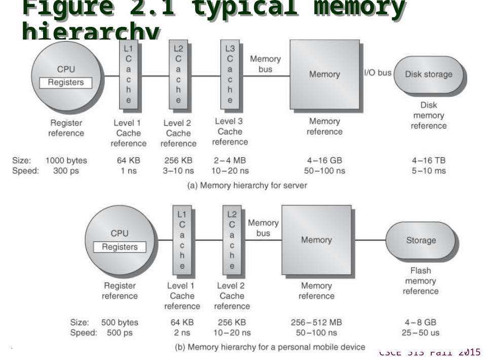
Figure 2.1 typical memory hierarchyFigure 2.1 typical memory hierarchy

– 9 – CSCE 513 Fall 2015
Regs
L1
d-cache
L1
i-cache
L2 unified cache
Core 0
Regs
L1
d-cache
L1
i-cache
L2 unified cache
Core 3
…
L3 unified cache
(shared by all cores)
Main memory
Processor package
Intel I-7 Quad Core - Memory HierarchyIntel I-7 Quad Core - Memory Hierarchy

– 10 – CSCE 513 Fall 2015
Intel I-7 Memory HierarchyIntel I-7 Memory Hierarchy
– 11 – CSCE 513 Fall 2015
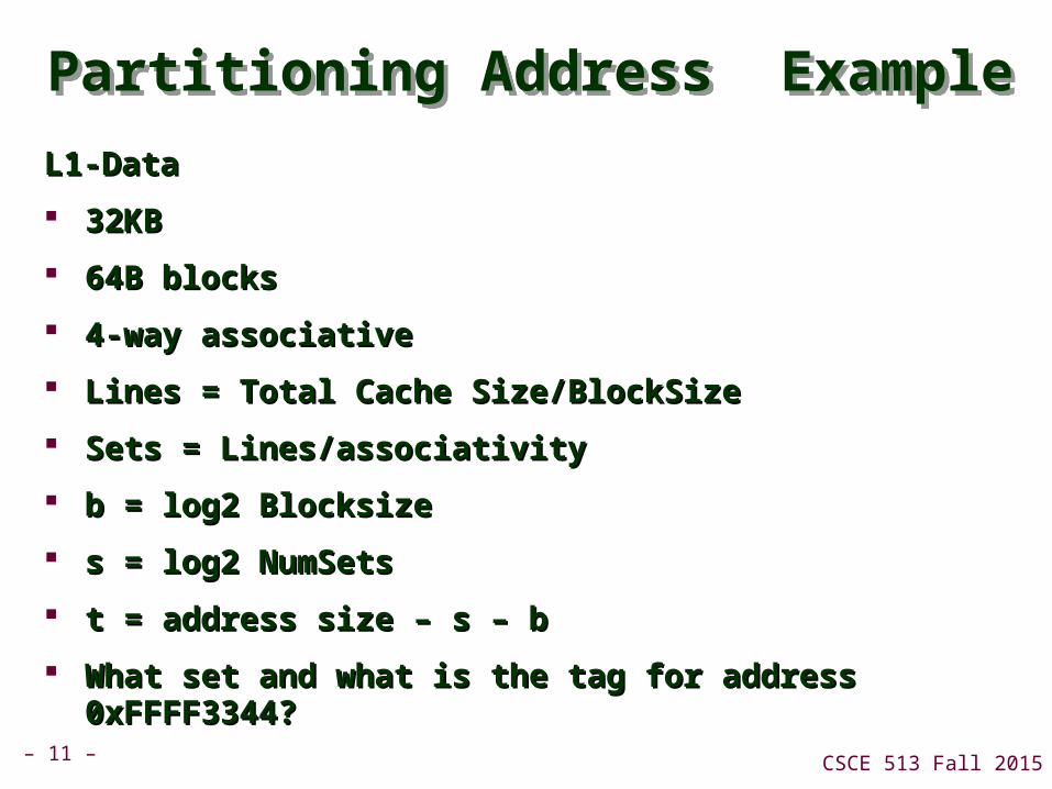
Partitioning Address ExamplePartitioning Address Example
L1-Data L1-Data
32KB32KB
64B blocks64B blocks
4-way associative4-way associative
Lines = Total Cache Size/BlockSizeLines = Total Cache Size/BlockSize
Sets = Lines/associativitySets = Lines/associativity
b = log2 Blocksizeb = log2 Blocksize
s = log2 NumSetss = log2 NumSets
t = address size – s – b t = address size – s – b
What set and what is the tag for address 0xFFFF3344?What set and what is the tag for address 0xFFFF3344?

– 12 – CSCE 513 Fall 2015
Cache Review – Appendix B TerminologyCache Review – Appendix B Terminologyfully associative fully associative write allocate write allocate virtual memory virtual memory dirty bit dirty bit unified cache unified cache memory stall cycles memory stall cycles block offset block offset misses per instruction misses per instruction direct mapped direct mapped write-back write-back valid bit valid bit locality allocate page locality allocate page least recently used least recently used write buffer write buffer miss penalty miss penalty
block address block address hit time hit time address trace address trace write-through write-through cache miss cache miss set set instruction cache instruction cache page fault page fault random replacement random replacement average memory access time average memory access time miss rate miss rate index field index field cache hit cache hit n-way set associative n-way set associative tag field tag field write stallwrite stall
– 13 – CSCE 513 Fall 2015
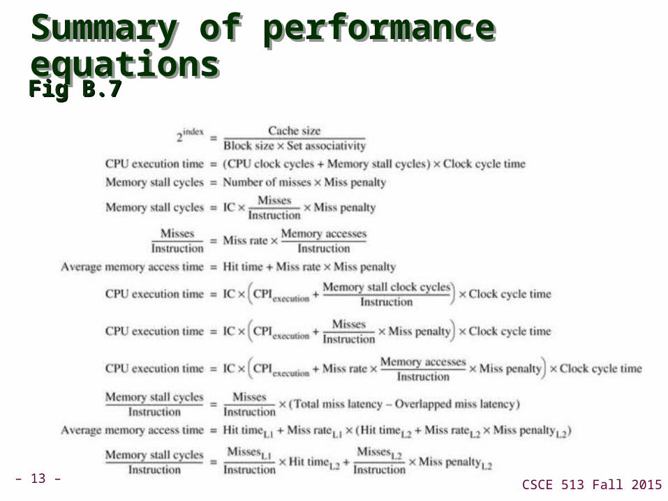
Summary of performance equations Summary of performance equations Fig B.7Fig B.7

– 14 – CSCE 513 Fall 2015
Figure B-4 data cache misses per 1000 instructionsFigure B-4 data cache misses per 1000 instructions..
– 15 – CSCE 513 Fall 2015
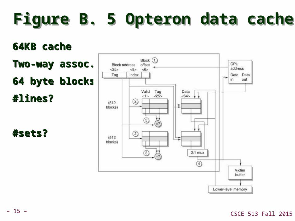
Figure B. 5 Opteron data cacheFigure B. 5 Opteron data cache
64KB cache64KB cache
Two-way assoc.Two-way assoc.
64 byte blocks64 byte blocks
#lines?#lines?
#sets?#sets?

– 16 – CSCE 513 Fall 2015
Figure B.6 Misses per 1000 instructionsFigure B.6 Misses per 1000 instructions

– 17 – CSCE 513 Fall 2015
Average Memory Access Time (AMAT)Average Memory Access Time (AMAT)
AMAT = HitTime + MissRate * MissPenaltyAMAT = HitTime + MissRate * MissPenalty
For two level cacheFor two level cache
AMAT = HT + MRAMAT = HT + MRL1L1*[HT*[HTL2L2 + MR + MRL2L2* MissPenalty* MissPenaltyL2L2]]

– 18 – CSCE 513 Fall 2015
ExampleExample
• CPI=1.0 always when we hit cacheCPI=1.0 always when we hit cache
• Loads/stores 50% of instructionsLoads/stores 50% of instructions
• MissPenalty=200 cyclesMissPenalty=200 cycles
• MissRate = 2%MissRate = 2%
• What is the AMAT?What is the AMAT?

– 19 – CSCE 513 Fall 2015
Pop QuizPop Quiz
Given L1-data cache 256KB, direct mapped, 64B Given L1-data cache 256KB, direct mapped, 64B blocks, hit_rate=.9, miss_penalty = 10 cyclesblocks, hit_rate=.9, miss_penalty = 10 cycles
1.1. What is size of block offset field?What is size of block offset field?
2.2. What is the size of the set_index field?What is the size of the set_index field?
3.3. If the Virtual address is 32 bits what is the size of the If the Virtual address is 32 bits what is the size of the tag field?tag field?
4.4. Given the address 0x00FF03b4 what is theGiven the address 0x00FF03b4 what is the• Block offset field• Set-index field• Tag field
5.5. AMAT = ? In cyclesAMAT = ? In cycles

– 20 – CSCE 513 Fall 2015
Virtual memory reviewVirtual memory review
Cache analogyCache analogy
Software versus HardwareSoftware versus Hardware

– 21 – CSCE 513 Fall 2015Copyright © 2011, Elsevier Inc. All rights Reserved.
Figure B.19 The logical program in its contiguous virtual address space is shown on the left. It consists of four pages, A, B, C, and D. The actual location of three of the blocks is in physical main memory and
the other is located on the disk.

– 22 – CSCE 513 Fall 2015
Translation Lookaside BuffersTranslation Lookaside Buffers
– 23 – CSCE 513 Fall 2015
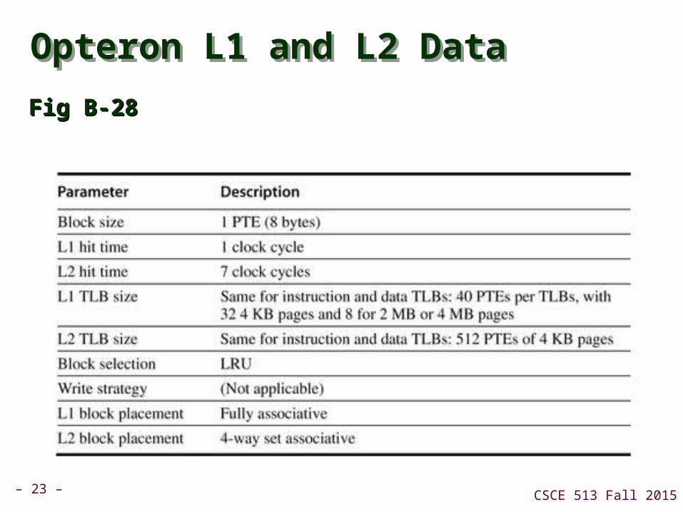
Opteron L1 and L2 DataOpteron L1 and L2 Data
Fig B-28Fig B-28
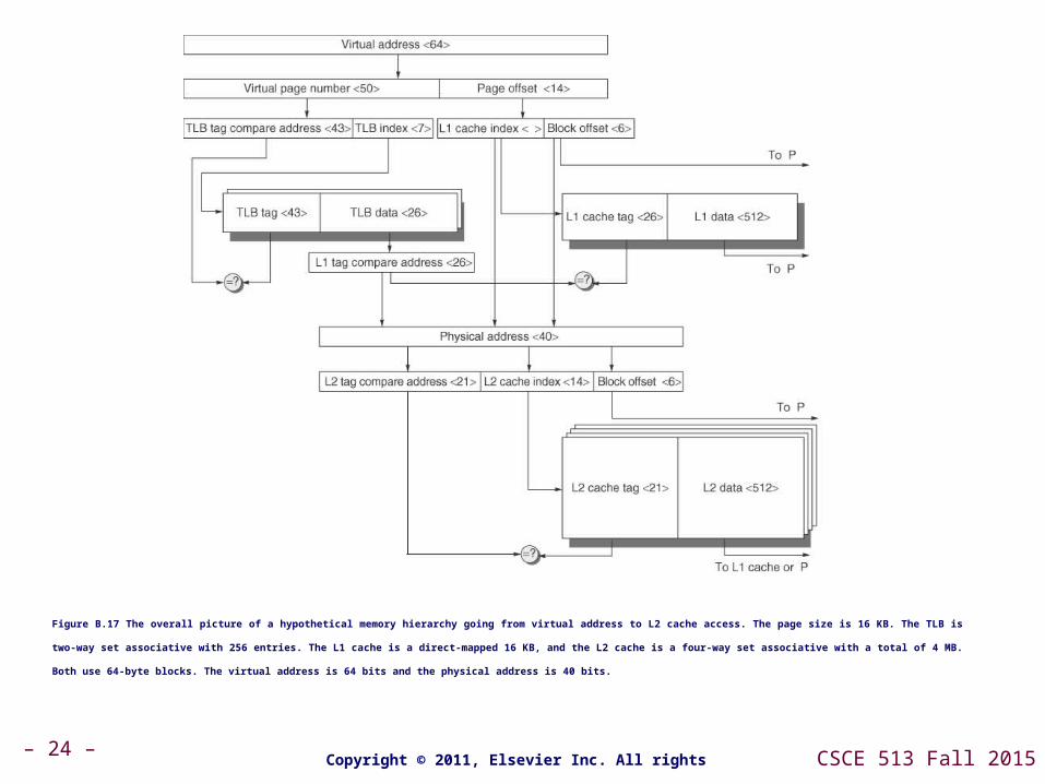
– 24 – CSCE 513 Fall 2015Copyright © 2011, Elsevier Inc. All rights Reserved.
Figure B.17 The overall picture of a hypothetical memory hierarchy going from virtual address to L2 cache access. The page size is 16 KB. The TLB is two-way set associative with 256 entries. The L1 cache is a
direct-mapped 16 KB, and the L2 cache is a four-way set associative with a total of 4 MB. Both use 64-byte blocks. The virtual address is 64 bits and the physical address is 40 bits.
– 25 – CSCE 513 Fall 2015
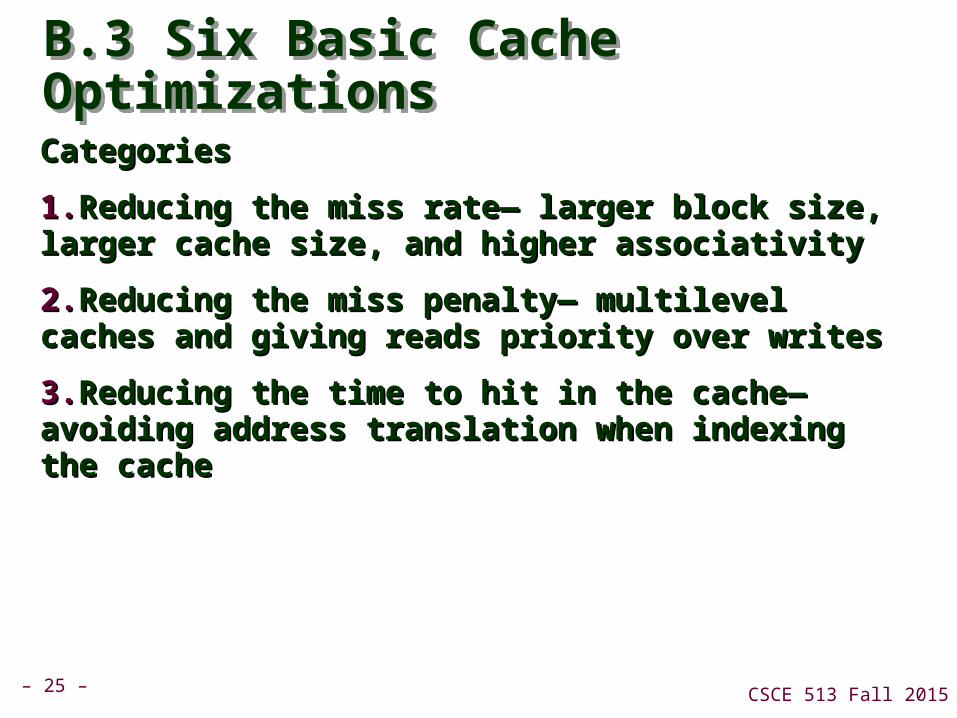
B.3 Six Basic Cache OptimizationsB.3 Six Basic Cache Optimizations
CategoriesCategories
1.1.Reducing the miss rate— larger block size, larger Reducing the miss rate— larger block size, larger cache size, and higher associativity cache size, and higher associativity
2.2.Reducing the miss penalty— multilevel caches and Reducing the miss penalty— multilevel caches and giving reads priority over writes giving reads priority over writes
3.3.Reducing the time to hit in the cache— avoiding Reducing the time to hit in the cache— avoiding address translation when indexing the cacheaddress translation when indexing the cache
– 26 – CSCE 513 Fall 2015
Optimization 1 – Larger Block Size to Reduce Miss Rate Optimization 1 – Larger Block Size to Reduce Miss Rate
– 27 – CSCE 513 Fall 2015
Optimization 2 - Larger Caches to Reduce Miss Rate Optimization 2 - Larger Caches to Reduce Miss Rate
– 28 – CSCE 513 Fall 2015
Optimization 3 – Higher Associativity to reduce Miss RateOptimization 3 – Higher Associativity to reduce Miss Rate

– 29 – CSCE 513 Fall 2015
Optimization 4 - Multilevel Caches to Reduce Miss PenaltyOptimization 4 - Multilevel Caches to Reduce Miss Penalty

– 30 – CSCE 513 Fall 2015
Optimization 5 – Giving Priority to Read Misses over Write misses to reduce Miss Penalty
Optimization 5 – Giving Priority to Read Misses over Write misses to reduce Miss Penalty

– 31 – CSCE 513 Fall 2015
Optimization 6 - Avoiding Address Translation during indexing of the Cache to reduce Hit time
Optimization 6 - Avoiding Address Translation during indexing of the Cache to reduce Hit timeFig B.17Fig B.17
– 32 – CSCE 513 Fall 2015
Figure 2.1 typical memory hierarchyFigure 2.1 typical memory hierarchy

– 33 – CSCE 513 Fall 2015
2.2 - 10 Advanced Cache Optimizations2.2 - 10 Advanced Cache Optimizations
Five CategoriesFive Categories
1.1.Reducing Hit Time-Small and simple first-level caches and way-Reducing Hit Time-Small and simple first-level caches and way-prediction. Both techniques also generally decrease power prediction. Both techniques also generally decrease power consumption. consumption.
2.2. Increasing cache bandwidth— Pipelined caches, multibanked Increasing cache bandwidth— Pipelined caches, multibanked caches, and nonblocking caches. These techniques have varying caches, and nonblocking caches. These techniques have varying impacts on power consumption. impacts on power consumption.
3.3.Reducing the miss penalty— Critical word first and merging write Reducing the miss penalty— Critical word first and merging write buffers. These optimizations have little impact on power. buffers. These optimizations have little impact on power.
4.4.Reducing the miss rate— Compiler optimizationsReducing the miss rate— Compiler optimizations
5.5.Reducing the miss penalty or miss rate via parallelism— Reducing the miss penalty or miss rate via parallelism— Hardware prefetching and compiler prefetching.Hardware prefetching and compiler prefetching.

– 34 – CSCE 513 Fall 2015
CAAQA 5th revistedCAAQA 5th revistedhttp://booksite.mkp.com/9780123838728/
Reference Appendices. Reference Appendices.
Appendix D: Storage Systems
Appendix E: Embedded Systems by Thomas M. Conte
Appendix F: Interconnection Networks updated by Timothy M. Pinkston and José Duato
Appendix G: Vector Processors by Krste Asanovic
Appendix H: Hardware and Software for VLIW and EPIC
Appendix I: Large-Scale Multiprocessors and Scientific Applications
Appendix J: Computer Arithmetic by David Goldberg
Appendix K: Survey of Instruction Set Architectures
Historical Perspectives with References. Appendix L Historical Perspectives with References. Appendix L
Lecture Slides. Lecture slides in PowerPoint (PPT) format are Lecture Slides. Lecture slides in PowerPoint (PPT) format are provided. These slides, developed by Jason Bakos of the provided. These slides, developed by Jason Bakos of the University of South Carolina, …University of South Carolina, …
http://booksite.mkp.com/9780123838728/

– 35 – CSCE 513 Fall 2015Copyright © 2012, Elsevier Inc. All rights reserved.
Memory Hierarchy Memory Hierarchy In
trod
uctio
n
– 36 – CSCE 513 Fall 2015Copyright © 2012, Elsevier Inc. All rights reserved.
Memory Hierarchy BasicsMemory Hierarchy Basics
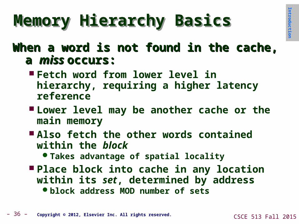
When a word is not found in the cache, a When a word is not found in the cache, a miss miss occurs:occurs: Fetch word from lower level in hierarchy, requiring
a higher latency reference Lower level may be another cache or the main
memory Also fetch the other words contained within the
blockTakes advantage of spatial locality
Place block into cache in any location within its set, determined by addressblock address MOD number of sets
Intro
du
ction

– 37 – CSCE 513 Fall 2015Copyright © 2012, Elsevier Inc. All rights reserved.
Memory Hierarchy BasicsMemory Hierarchy Basics
nn blocks per set => blocks per set => n-way set associativen-way set associative one block per set Direct-mapped cache Fully associative => one set
Writing to cache: two strategiesWriting to cache: two strategies Write-through
Immediately update lower levels of hierarchy Write-back
Only update lower levels of hierarchy when an updated block is replaced
Both strategies use write buffer to make writes asynchronous
Intro
du
ction
– 38 – CSCE 513 Fall 2015Copyright © 2012, Elsevier Inc. All rights reserved.
Memory Hierarchy BasicsMemory Hierarchy Basics
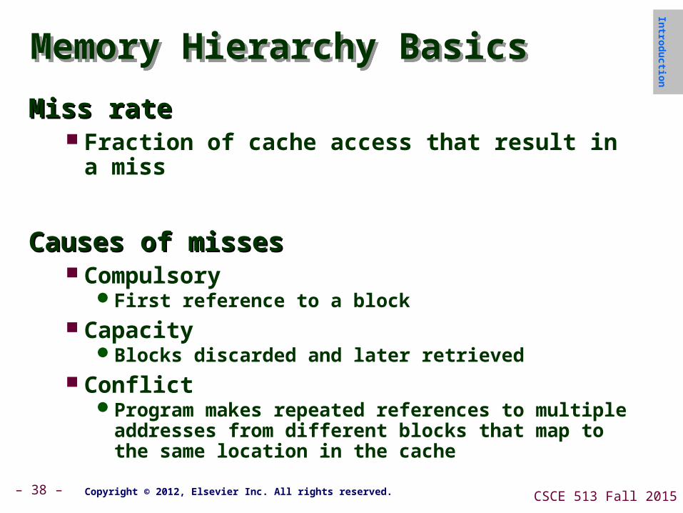
Miss rateMiss rate Fraction of cache access that result in a miss
Causes of missesCauses of misses Compulsory
First reference to a block Capacity
Blocks discarded and later retrieved Conflict
Program makes repeated references to multiple addresses from different blocks that map to the same location in the cache
Intro
du
ction

– 39 – CSCE 513 Fall 2015
Note that speculative and multithreaded Note that speculative and multithreaded processors may execute other instructions processors may execute other instructions during a missduring a miss Reduces performance impact of misses
Copyright © 2012, Elsevier Inc. All rights reserved.
Memory Hierarchy BasicsMemory Hierarchy BasicsIn
trod
uctio
n

– 40 – CSCE 513 Fall 2015Copyright © 2012, Elsevier Inc. All rights reserved.
Memory Hierarchy Basics (Appendix B)Memory Hierarchy Basics (Appendix B)
Six basic cache optimizations:Six basic cache optimizations: Larger block size
Reduces compulsory misses Increases capacity and conflict misses, increases miss penalty
Larger total cache capacity to reduce miss rate Increases hit time, increases power consumption
Higher associativity Reduces conflict misses Increases hit time, increases power consumption
Higher number of cache levels Reduces overall memory access time
Giving priority to read misses over writes Reduces miss penalty
Avoiding address translation in cache indexing Reduces hit time
Intro
du
ction

– 41 – CSCE 513 Fall 2015Copyright © 2012, Elsevier Inc. All rights reserved.
Ten Advanced OptimizationsTen Advanced Optimizations
Small and simple first level cachesSmall and simple first level caches Critical timing path:
addressing tag memory, thencomparing tags, thenselecting correct set
Direct-mapped caches can overlap tag compare and transmission of data
Lower associativity reduces power because fewer cache lines are accessed
Ad
vanced
Op
timizatio
ns

– 42 – CSCE 513 Fall 2015Copyright © 2012, Elsevier Inc. All rights reserved.
L1 Size and AssociativityL1 Size and Associativity
Access time vs. size and associativity
Ad
vanced
Op
timizatio
ns

– 43 – CSCE 513 Fall 2015Copyright © 2012, Elsevier Inc. All rights reserved.
L1 Size and AssociativityL1 Size and Associativity
Energy per read vs. size and associativity
Ad
vanced
Op
timizatio
ns

– 44 – CSCE 513 Fall 2015Copyright © 2012, Elsevier Inc. All rights reserved.
Way PredictionWay Prediction
To improve hit time, predict the way to pre-set To improve hit time, predict the way to pre-set muxmux Mis-prediction gives longer hit time Prediction accuracy
> 90% for two-way> 80% for four-wayI-cache has better accuracy than D-cache
First used on MIPS R10000 in mid-90s Used on ARM Cortex-A8
Extend to predict block as wellExtend to predict block as well “Way selection” Increases mis-prediction penalty
Ad
vanced
Op
timizatio
ns

– 45 – CSCE 513 Fall 2015Copyright © 2012, Elsevier Inc. All rights reserved.
Pipelining CachePipelining Cache
Pipeline cache access to improve bandwidthPipeline cache access to improve bandwidth Examples:
Pentium: 1 cyclePentium Pro – Pentium III: 2 cyclesPentium 4 – Core i7: 4 cycles
Increases branch mis-prediction penaltyIncreases branch mis-prediction penalty
Makes it easier to increase associativityMakes it easier to increase associativity
Ad
vanced
Op
timizatio
ns

– 46 – CSCE 513 Fall 2015Copyright © 2012, Elsevier Inc. All rights reserved.
Nonblocking CachesNonblocking CachesAllow hits before Allow hits before
previous misses previous misses completecomplete “Hit under miss” “Hit under multiple
miss”
L2 must support thisL2 must support this
In general, In general, processors can processors can hide L1 miss hide L1 miss penalty but not L2 penalty but not L2 miss penaltymiss penalty
Ad
vanced
Op
timizatio
ns

– 47 – CSCE 513 Fall 2015Copyright © 2012, Elsevier Inc. All rights reserved.
Multibanked CachesMultibanked Caches
Organize cache as independent banks to Organize cache as independent banks to support simultaneous accesssupport simultaneous access ARM Cortex-A8 supports 1-4 banks for L2 Intel i7 supports 4 banks for L1 and 8 banks for
L2
Interleave banks according to block addressInterleave banks according to block address
Ad
vanced
Op
timizatio
ns

– 48 – CSCE 513 Fall 2015Copyright © 2012, Elsevier Inc. All rights reserved.
Critical Word First, Early RestartCritical Word First, Early Restart
Critical word firstCritical word first Request missed word from memory first Send it to the processor as soon as it arrives
Early restartEarly restart Request words in normal order Send missed work to the processor as soon as
it arrives
Effectiveness of these strategies depends Effectiveness of these strategies depends on block size and likelihood of another on block size and likelihood of another access to the portion of the block that has access to the portion of the block that has not yet been fetchednot yet been fetched
Ad
vanced
Op
timizatio
ns

– 49 – CSCE 513 Fall 2015Copyright © 2012, Elsevier Inc. All rights reserved.
Merging Write BufferMerging Write BufferWhen storing to a block that is already pending in When storing to a block that is already pending in
the write buffer, update write bufferthe write buffer, update write buffer
Reduces stalls due to full write bufferReduces stalls due to full write buffer
Do not apply to I/O addressesDo not apply to I/O addresses
Ad
vanced
Op
timizatio
ns
No write buffering
Write buffering

– 50 – CSCE 513 Fall 2015Copyright © 2012, Elsevier Inc. All rights reserved.
Compiler OptimizationsCompiler Optimizations
Loop InterchangeLoop Interchange Swap nested loops to access memory in
sequential order
BlockingBlocking Instead of accessing entire rows or columns,
subdivide matrices into blocks Requires more memory accesses but improves
locality of accesses
Ad
vanced
Op
timizatio
ns

– 51 – CSCE 513 Fall 2015Copyright © 2012, Elsevier Inc. All rights reserved.
Hardware PrefetchingHardware Prefetching
Fetch two blocks on miss (include next Fetch two blocks on miss (include next sequential block)sequential block)
Ad
vanced
Op
timizatio
ns
Pentium 4 Pre-fetching

– 52 – CSCE 513 Fall 2015Copyright © 2012, Elsevier Inc. All rights reserved.
Compiler PrefetchingCompiler PrefetchingInsert prefetch instructions before data is Insert prefetch instructions before data is
neededneeded
Non-faulting: prefetch doesn’t cause Non-faulting: prefetch doesn’t cause exceptionsexceptions
Register prefetchRegister prefetch Loads data into register
Cache prefetchCache prefetch Loads data into cache
Combine with loop unrolling and software Combine with loop unrolling and software pipeliningpipelining
Ad
vanced
Op
timizatio
ns

– 53 – CSCE 513 Fall 2015Copyright © 2012, Elsevier Inc. All rights reserved.
SummarySummary Ad
vanced
Op
timizatio
ns

– 54 – CSCE 513 Fall 2015Copyright © 2012, Elsevier Inc. All rights reserved.
Memory TechnologyMemory Technology
Performance metricsPerformance metrics Latency is concern of cache Bandwidth is concern of multiprocessors and
I/O Access time
Time between read request and when desired word arrives
Cycle timeMinimum time between unrelated requests to
memory
DRAM used for main memory, SRAM used DRAM used for main memory, SRAM used for cachefor cache
Mem
ory T
echn
olo
gy

– 55 – CSCE 513 Fall 2015Copyright © 2012, Elsevier Inc. All rights reserved.
Memory TechnologyMemory Technology
SRAMSRAM Requires low power to retain bit Requires 6 transistors/bit
DRAMDRAM Must be re-written after being read Must also be periodically refeshed
Every ~ 8 msEach row can be refreshed simultaneously
One transistor/bit Address lines are multiplexed:
Upper half of address: row access strobe (RAS)Lower half of address: column access strobe (CAS)
Mem
ory T
echn
olo
gy

– 56 – CSCE 513 Fall 2015Copyright © 2012, Elsevier Inc. All rights reserved.
Memory TechnologyMemory TechnologyAmdahl:Amdahl:
Memory capacity should grow linearly with processor speed
Unfortunately, memory capacity and speed has not kept pace with processors
Some optimizations:Some optimizations: Multiple accesses to same row Synchronous DRAM
Added clock to DRAM interfaceBurst mode with critical word first
Wider interfaces Double data rate (DDR) Multiple banks on each DRAM device
Mem
ory T
echn
olo
gy
– 57 – CSCE 513 Fall 2015Copyright © 2012, Elsevier Inc. All rights reserved.
Memory OptimizationsMemory OptimizationsM
emo
ry Tech
no
log
y

– 58 – CSCE 513 Fall 2015Copyright © 2012, Elsevier Inc. All rights reserved.
Memory OptimizationsMemory OptimizationsM
emo
ry Tech
no
log
y

– 59 – CSCE 513 Fall 2015Copyright © 2012, Elsevier Inc. All rights reserved.
Memory OptimizationsMemory Optimizations
DDR:DDR: DDR2
Lower power (2.5 V -> 1.8 V)Higher clock rates (266 MHz, 333 MHz, 400 MHz)
DDR31.5 V800 MHz
DDR41-1.2 V1600 MHz
GDDR5 is graphics memory based on DDR3GDDR5 is graphics memory based on DDR3
Mem
ory T
echn
olo
gy

– 60 – CSCE 513 Fall 2015
DDR4 SDRAMDDR4 SDRAM
DDR4 SDRAM, an DDR4 SDRAM, an abbreviation for double data rate fourth for double data rate fourth generation synchronous dynamic random-access generation synchronous dynamic random-access memory, is a type of memory, is a type of synchronous dynamic random-access memory (SDRAM) (SDRAM) with a high with a high bandwidth (" ("double data rate") interface. It ") interface. It was released to the market in 2014was released to the market in 2014
Benefits include Benefits include • higher module density and lower voltage requirements, • coupled with higher data rate transfer speeds. • DDR4 operates at a voltage of 1.2V with frequency between 1600
and 3200 MHz, compared to frequency between 800 and 2133 MHz and voltage requirement of 1.5 or 1.65V of DDR3.
• DDR4 modules can also be manufactured at twice the density of DDR3.
http://en.wikipedia.org/wiki/DDR4_SDRAM

– 61 – CSCE 513 Fall 2015Copyright © 2012, Elsevier Inc. All rights reserved.
Memory OptimizationsMemory Optimizations
Graphics memory:Graphics memory: Achieve 2-5 X bandwidth per DRAM vs. DDR3
Wider interfaces (32 vs. 16 bit)Higher clock rate
» Possible because they are attached via soldering instead of socketted DIMM modules
Reducing power in SDRAMs:Reducing power in SDRAMs: Lower voltage Low power mode (ignores clock, continues to
refresh)
Mem
ory T
echn
olo
gy

– 62 – CSCE 513 Fall 2015Copyright © 2012, Elsevier Inc. All rights reserved.
Memory Power ConsumptionMemory Power ConsumptionM
emo
ry Tech
no
log
y

– 63 – CSCE 513 Fall 2015Copyright © 2012, Elsevier Inc. All rights reserved.
Flash MemoryFlash Memory
Type of EEPROMType of EEPROM
Must be erased (in blocks) before being Must be erased (in blocks) before being overwrittenoverwritten
Non volatileNon volatile
Limited number of write cyclesLimited number of write cycles
Cheaper than SDRAM, more expensive than Cheaper than SDRAM, more expensive than diskdisk
Slower than SRAM, faster than diskSlower than SRAM, faster than disk
Mem
ory T
echn
olo
gy

– 64 – CSCE 513 Fall 2015
Understand ReadyBoost and whether it will Speed Up your SystemUnderstand ReadyBoost and whether it will Speed Up your SystemWindows 7 supports Windows ReadyBoost. Windows 7 supports Windows ReadyBoost.
• This feature uses external USB flash drives as a hard disk cache to improve disk read performance.
• Supported external storage types include USB thumb drives, SD cards, and CF cards.
• Since ReadyBoost will not provide a performance gain when the primary disk is an SSD, Windows 7 disables ReadyBoost when reading from an SSD drive.
External storage must meet the following requirements:External storage must meet the following requirements:• Capacity of at least 256 MB, with at least 64 kilobytes (KB) of
free space. The 4-GB limit of Windows Vista has been removed.
• At least a 2.5 MB/sec throughput for 4-KB random reads• At least a 1.75 MB/sec throughput for 1-MB random writes
http://technet.microsoft.com/en-us/magazine/ff356869.aspx

– 65 – CSCE 513 Fall 2015Copyright © 2012, Elsevier Inc. All rights reserved.
Memory DependabilityMemory Dependability
Memory is susceptible to cosmic raysMemory is susceptible to cosmic rays
Soft errorsSoft errors: dynamic errors: dynamic errors Detected and fixed by error correcting codes
(ECC)
Hard errorsHard errors: permanent errors: permanent errors Use sparse rows to replace defective rows
Chipkill: a RAID-like error recovery Chipkill: a RAID-like error recovery techniquetechnique
Mem
ory T
echn
olo
gy

– 66 – CSCE 513 Fall 2015
Solid State DrivesSolid State Drives
http://en.wikipedia.org/wiki/Solid-state_drive
http://www.tomshardware.com/charts/hard-drives-and-ssds,3.html
• Hard Drives 34 dimensions: eg Desktop performance• SSD -

– 67 – CSCE 513 Fall 2015
Windows Experience IndexWindows Experience Index
Control Panel\All Control Panel Items\Performance Control Panel\All Control Panel Items\Performance Information and ToolsInformation and Tools
Control Panel\All Control Panel Items\Performance Information and Tools

– 68 – CSCE 513 Fall 2015
Windows Experience Index with Solid State Disk DriveWindows Experience Index with Solid State Disk Drive

– 69 – CSCE 513 Fall 2015